
 Open Access Article
 This Open Access Article is licensed under a Creative Commons Attribution-Non Commercial 3.0 Unported Licence
Multiple morphologies and functionality of nanowires made from earth-abundant zinc phosphide†
Simon
Escobar Steinvall
 a,
Nicolas
Tappy
a,
Masoomeh
Ghasemi
b,
Reza R.
Zamani
c,
Thomas
LaGrange
c,
Elias Z.
Stutz
a,
Jean-Baptiste
Leran
a,
Mahdi
Zamani
a,
Rajrupa
Paul
a and
Anna
Fontcuberta i Morral
*ad
a,
Nicolas
Tappy
a,
Masoomeh
Ghasemi
b,
Reza R.
Zamani
c,
Thomas
LaGrange
c,
Elias Z.
Stutz
a,
Jean-Baptiste
Leran
a,
Mahdi
Zamani
a,
Rajrupa
Paul
a and
Anna
Fontcuberta i Morral
*ad
aLaboratory of Semiconductor Materials, Institute of Materials, École Polytechnique Fédérale de Lausanne, 1015 Lausanne, Switzerland. E-mail: anna.fontcuberta-morral@epfl.ch
bThermo-Calc Software AB, 169 67 Solna, Sweden
cCentre Interdisciplinaire de Microscopie Électronique, École Polytechnique Fédérale de Lausanne, 1015 Lausanne, Switzerland
dInstitute of Physics, École Polytechnique Fédérale de Lausanne, 1015 Lausanne, Switzerland
First published on 8th October 2019
Abstract
Semiconductors made of earth-abundant elements, such as zinc phosphide, have the potential to substitute less abundant, highly functional compound semiconductors such as InAs or InP. Compound semiconductors in the form of nanowires could revolutionise application areas such as energy harvesting and optoelectronics. Here we synthesise Zn3P2 nanowires tailored in four different morphologies, namely vertical, straight-titled, zigzag and crawling. The optical properties elucidated by cathodoluminescence spectroscopy indicate a shape and V/II ratio dependence. Band-edge, defects, or surface nanoclusters mediate the luminescence in different degrees. This work opens new avenues for the use of earth-abundant Zn3P2 nanowires in photovoltaic applications.
New conceptsThe deployment of Zn3P2 as a photovoltaic absorber material has been limited by its lattice parameter and thermal expansion coefficient which are mismatched to commercially available substrates. In this work, we show for the first time the epitaxial growth of high-quality Zn3P2 nanowires. The nanowire form provides a way to circumvent the need of such an ideal substrate. By controlling the fluxes and substrate temperature we tailor the nanowire morphology, orientation, composition and optical properties. We thus provide a new avenue to integrate this functional and earth-abundant compound semiconductor for energy harvesting applications. |
Introduction
Zinc phosphide (Zn3P2) is an earth-abundant semiconductor with optoelectronic properties suitable for photovoltaic applications.1,2 It exhibits a direct bandgap of roughly 1.5 eV, strong absorption in the visible range of the electromagnetic spectrum, and carrier diffusion lengths in the order of 5–10 μm.3–8 Despite its promising properties, there has been limited progress in the fabrication of high-quality zinc phosphide devices. The highest photovoltaic conversion efficiency achieved using a Zn3P2 absorber was ∼6%, which was achieved several decades ago.9 There are three main challenges with the processing of this earth-abundant semiconductor, the first being its large tetragonal unit cell (a = 8.089 Å, c = 11.45 Å), complicating epitaxial growth.10 The second arises from its high thermal expansion coefficient (1.4 × 10⁻⁵ K−1) which introduces strain and defects upon cooling after growth.11,12 The final challenge involves achieving controllable doping. Most growth techniques result in intrinsic p-type doping through phosphorus interstitials. Extrinsic doping, particularly n-type, is not yet fully unravelled.13–15To overcome these challenges, the nanowire morphology shows promising perspectives. First, their small diameter allows for high-quality epitaxial growth on lattice mismatched substrates through radial stress relaxation.16–18 These factors mitigate the challenges posed by II3V2's large lattice parameter and coefficient of thermal expansion, facilitating virtually defect-free epitaxial growth.19,20 Moreover, vertical nanowire arrays exhibit photonic properties enabling increased light absorption with respect to the equivalent thin film.21–29 This is a consequence of their enhanced absorption cross-section, and modification of light emission directivity. Altogether, this modifies the Shockley–Queisser limit, resulting in a higher theoretical efficiency for nanowire devices compared to planar ones.21–29
In this work, we demonstrate the growth of Zn3P2 nanowires in tailored morphologies using molecular beam epitaxy (MBE). The use of MBE lowers growth temperatures in comparison to other techniques used to obtain Zn3P2, such as chemical vapour transport in a quartz ampule and metal–organic chemical vapour deposition.11,30–32 The lower growth temperature should significantly reduce the number of grown-in defects induced by strain from differential thermal expansion. Furthermore, by varying the V/II flux ratio in the MBE, the composition of thin films can be adjusted precisely. This is the key to control the density of self-interstitials, which readily form due to the high number of large vacant sites in the zinc sublattice, and thus the degree of intrinsic doping due to deviations from stoichiometry.30 In principle, the precise flux control in MBE should also enable the controlled incorporation of extrinsic dopants such as Ag, Mg and In.13,14,33–35
Previously, in addition to thin films and bulk crystals, Zn3P2 has been obtained in the form of randomly oriented nanowires, nanoribbons, and nanotrumpets.36–43 In most of these studies, nanowires were produced through chemical vapour deposition (CVD) or by a thermochemical method relying on a quartz capsule containing the precursors being heated in a furnace.36,37,39–41,43 Both of these techniques result in a nanowire powder consisting of randomly aligned nanowires not attached to a substrate. To achieve the 1D nanowire morphology, researchers have mainly relied on the vapour–liquid–solid (VLS) growth mechanism, where a nanoscale liquid catalyst is used to guide 1D growth through enhanced precursor absorption and selective, directional precipitation upon supersaturation.44 The catalysts previously reported for zinc phosphide nanowire growth are gold, indium and tin.36,39–41,45 Whilst gold catalysed nanowires tend to be straight, those grown with indium and tin exhibited a zigzag morphology.36,39,40,45 Similar superlattice structures have also been reported for other compound semiconductors. According to Algra et al., twinning minimises the deformation of the droplet on the top facet when the cross-section reaches a truncated triangular geometry, and turns it back to a hexagon.46–48
Proper selection of the substrate with suitable crystal structure can promote epitaxial growth. InP(1 0 0) has been proposed as a suitable substrate due to the low mismatch between the phosphorus sublattices. It also avoids the formation of an interfacial phosphide, as was observed on GaAs.49,50
Here, we report the epitaxial growth of zinc phosphide nanowires by MBE, in various morphologies. To the best of our knowledge, this is the first report on the growth of tuneable epitaxial Zn3P2 nanowires by MBE.
Results and discussion
Zn3−xP2+y nanowires were obtained in 4 different morphologies on InP(1 0 0), which we denominate as vertical, straight-tilted, zigzag, and crawling. Scanning electron microscopy (SEM) images of the different morphologies are presented in Fig. 1a–d, respectively, with lower magnification images included in the ESI.† The vertical nanowire morphology is ideal for potential photovoltaic applications because of their enhanced light absorption mentioned previously. Fig. 1e maps the different morphologies yielded as a function of the different growth conditions, i.e. manipulator temperature and V/II ratio. From here on, the reported V/II ratio corresponds to the ratio between the values of Zn and P2 beam equivalent pressures (BEPs). There is some overlap between the morphologies yielded, but the overall trends are as follows: at lower temperatures, the straight-tilted morphology dominates. At higher temperatures, on the other hand, the dominating morphology is the crawling nanowires, which is also the main type of wires for low V/II ratios. The zigzag nanowires grow mainly at moderate temperatures at intermediate V/II ratios, and the vertical morphology is similarly favoured at moderate temperatures, being the dominant morphology in the higher V/II ratio range. When the V/II ratio exceeds 1.6, a thin film overgrowing the nanoparticles is observed, as shown in the ESI.†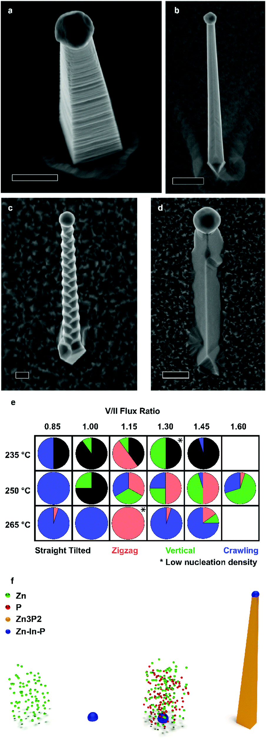 | ||
| Fig. 1 (a)–(d) are SEM images of vertical, straight-tilted, zigzag and crawling nanowires with scale bars of 500 nm. The first image is at 20°, whilst the others are normal to the substrate. (e) Shows the growth condition and manipulator temperature combination which resulted in what morphologies and (f) is an illustration of the proposed growth mechanism. | ||
The vertical nanowires exhibit a significant surface roughness, which generally can be attributed to the presence of stacking faults. However, as it will be shown, this is not the case. Im et al. investigated Zn3P2 nanowires grown by either Au or In catalysed VLS, and they observed the formation of superlattices only in the latter.40 Similarly, Shen et al. also reported the formation of superlattice nanowires only when growing using an In catalyst.36 However, from this study it is clear that it is possible to achieve different morphologies by simply tuning the growth conditions and not the catalyst.
Fig. 1f illustrates is the proposed growth mechanism of the nanowires. First, during the pre-deposition step, the zinc flux reacts with the indium phosphide substrate, forming a Zn–In–P nanoparticle, shown in the ESI.† This acts as the liquid-phase catalyst for VLS growth during the subsequent growth step, resulting in the so-called substrate-mediated VLS growth. It is worth mentioning that the nanowire density of most samples remained constant irrespective of the growth condition. We suspected that In droplets would form preferentially at surface irregularities. To test this hypothesis, we exposed the substrates to short Ar ion beam treatments to increase the surface roughness and/or irregularities. Representative SEM micrographs of samples exposed for 0, 5, and 10 s are presented in Fig. 2a–c. The nanowire density increases by a factor of 16 and 82 times, respectively, reaching a nanowire density of 1 nanowire per 2.4 μm2.
 | ||
| Fig. 2 (a)–(c) are SEM images of nanowire ensembles obtained after 0 s (a), 5 s (b), and 10 s (c) argon ion beam exposure respectively. We observe an increase in nucleation density of 16× and 82× with respect to (a). All scale bars are 10 μm. | ||
To support the proposed growth mechanism, we performed scanning transmission electron microscopy (STEM) energy dispersive X-ray spectroscopy (EDX). Representative measurements of a nanowire tip are shown in Fig. 3a–d. The main component of the droplet is indeed In. The faceted nature of the catalyst indicates that at room temperature, where the STEM EDX measurements were carried out, the catalyst is solid.
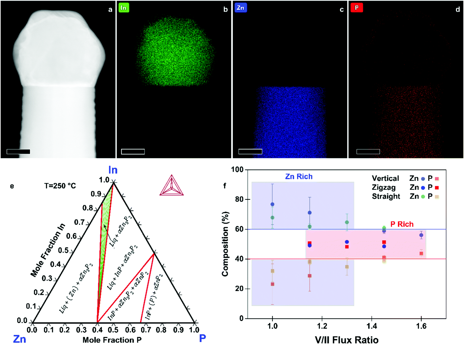 | ||
| Fig. 3 (a) HAADF STEM image of the top of a vertical nanowire. (b)–(d) Corresponding elemental map of indium, zinc and phosphorus. All scale bars are 50 nm. (e) Shows the ternary phase diagram of the Zn–In–P system calculated using the CALPHAD method at 250 °C. (f) Shows the deviation from stoichiometry of vertical nanowires grown at different V/II ratios. The straight lines indicate the ideal stoichiometry. The vertical and zigzag nanowires were grown at 250 °C, whilst the straight-titled ones were grown at 235 °C. | ||
To further elucidate the mechanisms at play we provide an understanding of the thermodynamic Zn–In–P system, obtained by the CALculation of PHAse Diagrams (CALPHAD) method.51 In the CALPHAD method, the Gibbs energies of the phases are modelled using experimental data as input. The equilibrium phase diagram is then mapped by minimisation of the Gibbs energies of the phases for all temperatures. One then finds the corresponding compositions of the phases with the lowest Gibbs energy. Although nanowire growth is a non-equilibrium process, thermodynamic diagrams provide information on what equilibrium phases can be obtained. The isothermal section of the Zn–In–P ternary phase diagram at 250 °C is presented in Fig. 3e. When adding Zn to InP, one moves into a tie triangle with liquid, InP and Zn3P2 phases present. The vertical section between Zn and InP, shown in the ESI,† indicates that a liquid phase is present above 156.3 °C. Below this temperature it undergoes an invariant transition, first forming Zn3P2 until the zinc in the droplet is consumed, which would preferentially nucleate at the interface of the already grown nanowire. The remaining In and P will then form an In (core) and InP (shell). These observations allow us to determine that our catalyst is indeed liquid during growth, and to explain the segregation observed in the catalyst at room temperature.
We now turn to the characterisation of the chemical composition of the nanowires as a function of the growth conditions and morphology, as measured by STEM EDX. The average composition of vertical, zigzag, and straight-tilted nanowires grown at different V/II ratios is presented in Fig. 3f, with the solid lines indicating the stoichiometric composition. The measurements were done for a rectangular section of an area approximately 100 × 100 nm2 and corrected for the thickness of the individual nanowires. Moreover, to accurately correct for the varying thickness of the zigzag nanowires, a polygon was used instead of a rectangle to cover an area of approximately constant thickness, and the measurements were taken using aberration corrected (AC) STEM. Low V/II ratios resulted in Zn-rich Zn3−xP2+y nanowires. The increase in P2 flux improves the homogeneity in composition and increase the P content, with the nanowires grown at a V/II ratio of 1.45 being closest to the stoichiometric composition. This sets MBE grown zinc phosphide apart from other growth techniques, which predominantly result in P-rich products.15,32 STEM EDX data of straight-tilted nanowires grown at 235 °C showed a similar trend. The zigzag nanowires, on the other hand, exhibit a 1![[thin space (1/6-em)]](https://www.rsc.org/images/entities/char_2009.gif) :1 ratio between Zn and P irrespective of the V/II ratio during growth. The composition along the nanowire did not change within the uncertainties of the measurement technique, as shown in the ESI.†
:1 ratio between Zn and P irrespective of the V/II ratio during growth. The composition along the nanowire did not change within the uncertainties of the measurement technique, as shown in the ESI.†
Growth temperatures below 235 °C result in randomly oriented nanowires, lacking a clear epitaxial relation with the substrate. Furthermore, in this temperature range, we observed nanowires with and without a droplet at the tip, indicating the possible coexistence of the previously mentioned VLS growth mechanism with a vapour–solid (VS) one. These nanowires presented a growth front consisting of exposed facets, similar to what is also found in GaAs.52 SEM images of these nanowires are presented in the ESI.†
Transmission electron microscopy (TEM) data for zigzag, straight-tilted, and vertical nanowires are presented in Fig. 4. Selective area electron diffraction (SAED) showed that all nanowires, irrespective of composition and morphology, have the P42/nmc crystal structure, characteristic of Zn3P2. Due to the thickness of vertical nanowires, they could not be characterised through high resolution (HR) TEM. However, SAED pattern analysis (Fig. 4m) indicates that the vertical nanowires have a [0 0 1] growth direction, whilst both zigzag and straight-tilted nanowires grow along the [1 0 1] direction (Fig. 4d and i). The [1 0 1] growth direction was also observed by Shen et al., Brockway et al., and Im et al..36,40,42 However, Im et al. also observed a [2 0 1] growth direction for their superlattice nanowires, and other studies have shown zinc phosphide nanowires growing along multiple other directions.36,40
 | ||
| Fig. 4 (a)–(d) HRTEM images of a zigzag nanowire grown at a V/II ratio of 1.30 at different magnification highlighting the superlattice formation along the growth axis and the superimposed SAED pattern along the [1 0 0] zone axis indicating a [1 0 1] growth direction. (a) Is rotated 90° with respect to the other images. (e) Shows a AC-HAADF STEM image inside a vertical nanowire, grown at a V/II ratio of 1.00, nanowire with an overlay of the zinc and phosphorus atoms as matched with the crystal structure as seen down the [1 0 0] axis (zinc is green and phosphorus red) alongside with an inset of the simulated structure. (f)–(i) Are HRTEM and SAED images of a straight-tilted nanowire grown at a V/II ratio of 1.00 as seen along the [1 0 0] zone axis, indicating a growth direction of [1 0 1], note, (e) is rotated 120° in relation to the other images. (j) Is an AC-HAADF STEM image of the surface of a vertical nanowire. (k)–(m) TEM images and the SAED pattern of a vertical nanowire along the [1 0 0] direction, indicating a growth direction along [0 0 1]. (n) Is the corresponding STEM EDX line scan going from the bulk (0 nm) to the surface and vacuum (20 nm). Scale bars in (a, f, k and l) are 200 nm. In (b, g and h) the scale bars are 10 nm, in (c) it is 5 nm, and finally in (e and j) they are 1 nm. | ||
HRTEM images from the zigzag nanowires (Fig. 4c and d) clearly show the superlattice structure. Structural defects were observed in the zigzag and straight-tilted nanowires (Fig. 4g–h). All structural defects observed in these nanowires were perpendicular to the [0 0 1] direction, and not to the growth direction. There was no preferential ordering observed in the frequency of these structural defects, indicating a more random generation mechanism as compared to the superlattices. A straight-tilted nanowire was also observed along the [1 1 1] zone axis, with the images presented in the ESI.† The defects were not observed along this zone axis as the Burgers vector of the defect and zone axis were not perpendicular.
In the case of the vertical nanowires, we were unable to determine the presence of structural defects through HRTEM investigations. A vertical nanowire obtained with a V/II ratio of 1.00 was investigated using AC high-angle annular dark field (AC-HAADF) STEM. In Fig. 4e, the bulk atomic arrangement as seen along the [1 0 0] zone axis of Zn3P2 is shown, with a zoomed out image presented in the ESI.† By comparing it with simulated HAADF STEM images along the [1 0 0] zone axis for different compositions in the Zn-rich range, presented in the ESI,† we confirm the [0 0 1] growth direction, in agreement with the SAED pattern in Fig. 4m. Furthermore, in low magnification images with the same resolution, we did not observe any stacking faults. The changes in the diameter of the nanowire around non-observed stacking faults may still explain the observed roughness, however, catalyst related effects are more probable.
Another aspect to note is that all nanowires exhibit tapering. There are two main mechanisms that result in tapered growth, either through the morphing of the catalyst or VS growth on the exposed facets. There are multiple pathways for the catalyst to shrink, and as the In catalyst is not replenished, its depletion during growth is an irreversible process. For example, In may evaporate. Given its low vapour pressure at the growth temperatures, we consider this an unlikely scenario. A more probable case is that the In catalyst is consumed during growth. In could potentially diffuse to the large vacant sites in the Zn3P2 lattice or to surface sites, depleting the In in the catalyst, and in turn reducing the nanowire diameter. We have indeed observed the presence of Zn3P2 VS growth on the side facets, however, we cannot rule out any catalyst related effects.
To ascertain if these processes occurred, we analysed the surface of the vertical nanowire using AC-HAADF STEM and EDX. Small clusters with a different crystal structure were observed scattered along the surface, as shown in Fig. 4j. Through an EDX line scan perpendicular to the surface in the aberration corrected HAADF STEM, Fig. 4n, we observed that the surface layer was enriched in indium. There were also significant amounts of phosphorus and oxygen present in these clusters. The symmetry of the AC-HAADF pattern, indicating a [1 1 0] zinc blende zone axis, and their composition suggest that In diffuses from the main catalyst to the surface of the nanowire during growth, reacting with the phosphorus flux, and generated InP nanoclusters. These clusters, and the overall surface of the nanowires, were covered by an amorphous oxide layer created during unloading from the MBE and exposure to air, as confirmed by the EDX line scan data shown in Fig. 4n. There is a sharp increase in phosphorus at the end of the line scan, but by correlating it to the HAADF intensity, we can deduce that it is an artefact of the quantification as the scan goes into the vacuum. To better understand the structure and distribution of these clusters, we applied fast Fourier transforms (FFT) and filters based on the symmetry to AC-HAADF STEM images, highlighting areas of different crystal symmetry (see ESI†). By adjusting the focus along the surface, we noted that some clusters were only observed at different focal depths, indicating a random and incomplete coverage of the surface with InP. Thus, we can deduce that the mechanism behind the consumption of In is through the formation of surface InP nanoclusters.
The tapering of the nanowires in itself is not an issue for photovoltaic applications; on the contrary, the range of diameters in a single nanowire allows the interaction between the nanowire optical absorption modes with an increased range of wavelengths.53–57 However, the nanoclusters may still act as a sink for either holes, electrons, or both depending on the alignment of the quantum dot energy level with the Zn3−xP2+y. Therefore, the nanoclusters may greatly influence the optoelectronic properties of the nanowires by selectively repelling one type of charge carrier whilst acting as a sink for the other, effectively quenching the luminescence. Still, they can potentially be removed by selective chemical etching. The tapering due to droplet reduction could be mitigated through an In flux of roughly 2–3 Å s−1, based on direct impingement similar to self-catalysed III–V nanowire growth.58,59
Finally, the optical properties of the nanowires were characterised by cathodoluminescence (CL) spectroscopy. In μ-photoluminescence studies, we did not observe any signal from the zinc phosphide, indicating high levels of non-radiative recombination. The higher excitation density of CL allowed us to observe radiative recombination, however, none indicative of bandgap recombination. The results from zigzag and vertical nanowires are presented in Fig. 5. In Fig. 5a–d, we present SEM micrographs and emission maps for zigzag and vertical nanowires. In the case of the zigzag nanowire, we observe emission localised at the nanowire, readily distinguishable from the background, as seen indicated in the CL map in Fig. 5b. The panchromatic CL map of the vertical nanowire, Fig. 5d, shows a different emission behaviour, with its emission mainly originating at the base of the nanowire.
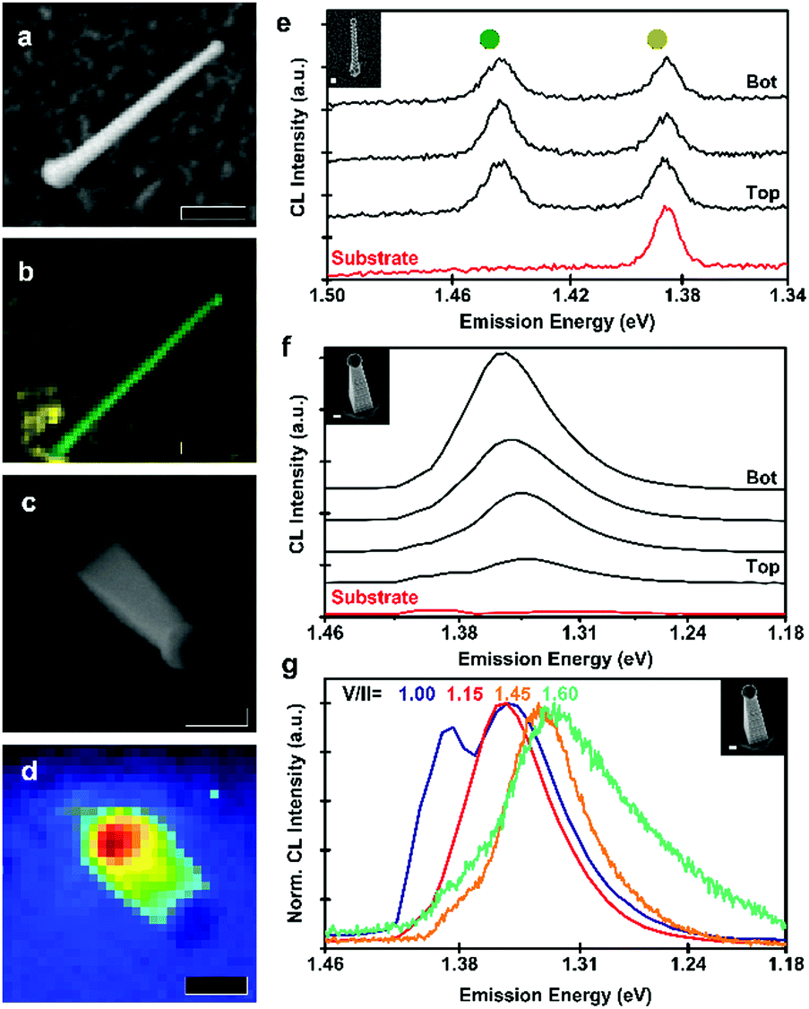 | ||
| Fig. 5 (a) is a SEM image of the zigzag nanowire analysed, and (b) shows a colour specific emission map of the zigzag nanowire, where green indicates the Zn3P2 emission whilst yellow is the background, InP, emission. (c) is a SEM image of a vertical nanowire grown at a V/II ratio of 1.15. (d) is an intensity map of the emission, showing higher intensity at the base of the nanowire. (e) is the spectra observed at different parts of the zigzag nanowire and also indicates the peak colouring in (b). (f) Shows the spectra taken from the different parts of the vertical nanowire in (c), and (g) shows normalised emission spectra from vertical nanowires grown at different V/II ratios. All scale bars are 500 nm. | ||
A detailed look into the CL spectra of the different parts of the nanowires is presented in Fig. 5e and f for a zigzag and vertical nanowire, respectively. For the zigzag nanowire, we observe a sharp emission at 1.43 eV (860 nm), this transition energy is lower than the reported direct bandgap of Zn3P2 of 1.50 eV, thus most likely originating from a defect transition.4–7 For the vertical nanowire, grown with a V/II ratio of 1.15, we observed that the main emission peak shifted from 1.35 eV (918 nm) at the base to 1.33 eV (928 nm) at the top, which could be a function of the tapering. These energies are also below the reported bandgap of Zn3P2, and similarly likely to originate from a defect transition. The InP nanoclusters may also be influencing the radiative recombination. Hence, further studies into the possible passivation of defects or removal of the surface nanoclusters are needed to optimise and clarify the optoelectronic response of the Zn3−xP2+y nanowires.
Fig. 5g depicts the emission of vertical nanowires as a function of V/II ratio. The emission peak redshifts with an increase of the V/II ratio. The main emission peak from the base of the nanowires shifts from 1.35 eV (917 nm) at low V/II ratios to 1.32 eV (940 nm) for higher V/II ratios. The peak shift could originate from different defect transitions in Zn-rich compared to P-rich samples. The emission from the nanowire grown at a V/II ratio of 1.00 also shows an emission peak at 1.38 eV (899 nm), which is attributed to recombination in the InP substrate. This could be a consequence of an enhanced carrier diffusion length of the nanowire, allowing for increased recombination at the substrate. These energies are in a similar range as self-interstitial related defect transitions reported previously, attributed to ionised acceptors.60 However, this would not explain the peak observed in Zn-rich samples (1.31 eV) or the shift with composition.
Conclusion
To summarise, we have obtained Zn3−xP2+y nanowires in four distinct tailored morphologies, among which the vertical nanowires are of particular interest for future photovoltaic applications. We have outlined the growth conditions yielding different nanowire morphologies and explained the substrate-mediated VLS growth mechanism through which they grow. We demonstrated the engineering of the chemical composition of the nanowires by the growth conditions (V/II ratio), which is crucial for control of the majority carrier type through intrinsic doping. TEM studies showed that the vertical nanowires grow along the [0 0 1] growth direction, whilst the straight-tilted and zigzag nanowires both grow along the [1 0 1] direction. The straight-tilted and zigzag nanowires also contained structural defects perpendicular to the [0 0 1] direction. The tapering of the nanowires was explained by shrinkage of the catalyst via the loss of In, which resulted in the formation of InP nanoclusters on the nanowire surface. Finally, using CL we observed an optical transition at 1.43 eV for zigzag nanowires, whilst the vertical nanowires showed a composition and location dependent emission in the range 1.32–1.35 eV. As the emission is observed at energies lower than the bandgap, their possible origin could be either defect transitions or recombination inside the surface InP nanoclusters. To yield more luminescent nanowires, further studies into passivation of the surface and of the nanoclusters are necessary.Methodology
Zn3−xP2+y nanowires were obtained in a Veeco GENxplor MBE system on InP(0 0 1) wafers using separate zinc and phosphorus sources (MBE Komponenten GaP-based P2 source). Before growth, the substrates were degassed at 580 °C for 10 minutes under a P2 atmosphere (beam equivalent pressure >1 × 10⁻⁶ Torr) to remove the native oxide, which was verified through reflective high-energy electron diffraction. Indium droplets were generated by a five-minute zinc pre-deposition with a flux of 3.4 × 10⁻⁷ Torr and at a manipulator temperature of 250 °C, where it can react and form a liquid phase. The nanowires were then grown for four hours at a manipulator temperature between 220–265 °C using a zinc BEP of 3.4 × 10⁻⁷ Torr and the P2 BEP was varied between 2.8–4.9 × 10⁻⁷ Torr. Ion beam etching of InP(0 0 1) wafers was done using a Veeco Nexus IBE350 system using an acceleration voltage of 700V and current of 1100 mA.The nanowires were characterised using a Zeiss Merlin FE-SEM, FEI Talos for conventional TEM/STEM operating at 200 kV, and FEI Titan Themis for AC STEM operating at 300 kV. The HAADF STEM images were filtered in Velox using a radial Weiner filter. 3D atomic models were generated using the Rhodius software package, and were then used for linear STEM image simulations.61 Using STEM_CELL we then performed STEM image simulations, relying on a modified version of the Kirkland “multislice” approach.62,63 An Attolight Rosa setup was used for CL measurements, operating at 10 K and using an acceleration voltage of 3 kV. Samples were loaded on a stage with 20° tilt, allowing us to observe the vertical nanowires. The ternary phase diagram of the Zn–In–P system was modelled based on existing thermodynamic descriptions from Lee, Ansara et al., and Ghasemi et al., and through extrapolation of the binary phase diagrams using Thermo-Calc.64–68 More details of the modelling of the phase diagrams via the CALPHAD method, applied to the Zn–P binary system, can be found in ref. 66 and the ESI.†
Conflicts of interest
There are no conflicts to declare.Acknowledgements
S. Escobar Steinvall, E. Stutz, R. Paul, M. Zamani and A. Fontcuberta i Morral were supported by the SNF Consolidator Grant (BSCGI0-157705). R. R. Zamani and T. LaGrange were supported by the EPFL-CIME. N. Tappy and A. Fonctuberta i Morral thank SNF funding through grant 20B2-1 176680. The authors also thank Anna Kúkol’ová for the SEM images of the initial catalyst particles.References
- C. Wadia, A. P. Alivisatos and D. M. Kammen, Environ. Sci. Technol., 2009, 43, 2072–2077 CrossRef CAS PubMed.
- J. Misiewicz, L. Bryja, K. Jezierski, J. Szatkowski, N. Mirowska, Z. Gumienny and E. Placzekpopko, Microelectron. J., 1994, 25, R23–R28 CrossRef.
- J. Pawlikowski, Phys. Rev. B: Condens. Matter Mater. Phys., 1982, 26, 4711–4713 CrossRef CAS.
- J. Misiewicz, J. Phys.: Condens. Matter, 1990, 2, 2053–2072 CrossRef CAS.
- J. Pawlikowski, Infrared Phys., 1981, 21, 181–187 CrossRef CAS.
- F. Briones, F. Wang and R. Bube, Appl. Phys. Lett., 1981, 39, 805–807 CrossRef CAS.
- G. M. Kimball, A. M. Mueller, N. S. Lewis and H. A. Atwater, Appl. Phys. Lett., 2009, 95, 112103 CrossRef.
- N. Wyeth and A. Catalano, J. Appl. Phys., 1979, 50, 1403–1407 CrossRef CAS.
- M. Bhushan and A. Catalano, Appl. Phys. Lett., 1981, 38, 39–41 CrossRef CAS.
- C. Pistorius, G. Clark, J. Ceotzer, G. Kruger and O. Kunze, High Pressure High Temp., 1977, 9, 471–482 CAS.
- J. Long, J. Electrochem. Soc., 1983, 130, 725–728 CrossRef CAS.
- T. Chu, S. Chu, K. Murthy, E. Stokes and P. Russell, J. Appl. Phys., 1983, 54, 2063–2068 CrossRef CAS.
- R. Katsube, H. Hayashi, A. Nagaoka, K. Yoshino, Y. Nose and Y. Shirai, Jpn. J. Appl. Phys., 2016, 55, 041201 CrossRef.
- R. Katsube, K. Kazumi, T. Tadokoro and Y. Nose, ACS Appl. Mater. Interfaces, 2018, 10, 36102–36107 CrossRef CAS.
- A. Catalano and R. Hall, J. Phys. Chem. Solids, 1980, 41, 635–640 CrossRef CAS.
- F. Glas, Phys. Rev. B: Condens. Matter Mater. Phys., 2006, 74, 121302 CrossRef.
- M. S. Gudiksen, L. J. Lauhon, J. Wang, D. C. Smith and C. M. Lieber, Nature, 2002, 415, 617–620 CrossRef CAS.
- M. T. Björk, B. J. Ohlsson, T. Sass, A. I. Persson, C. Thelander, M. H. Magnusson, K. Deppert, L. R. Wallenberg and L. Samuelson, Appl. Phys. Lett., 2002, 80, 1058–1060 CrossRef.
- T. Burgess, P. Caroff, Y. Wang, B. H. Badada, H. E. Jackson, L. M. Smith, Y. Guo, H. H. Tan and C. Jagadish, Nano Lett., 2015, 15, 378–385 CrossRef CAS.
- E. Z. Stutz, M. Friedl, T. Burgess, H. H. Tan, P. Caroff, C. Jagadish and A. Fontcuberta i Morral, Phys. Status Solidi RRL, 2019, 1900084 CrossRef.
- S. A. Mann, R. R. Grote, R. M. Osgood Jr., A. Alu and E. C. Garneet, ACS Nano, 2016, 10, 8620–8631 CrossRef CAS.
- A. Dorodnyy, E. Alarcon-Llado, V. Shklover, C. Hafner, A. Fontcuberta i Morral and J. Leuthold, ACS Photonics, 2015, 2, 1284–1288 CrossRef CAS.
- R. Frederiksen, G. Tutuncuoglu, F. Matteini, K. L. Martinez, A. Fontcuberta i Morral and E. Alarcon-Llado, ACS Photonics, 2017, 4, 2235–2241 CrossRef CAS.
- B. Kayes, H. Atwater and N. Lewis, J. Appl. Phys., 2005, 97, 114302 CrossRef.
- L. Hu and G. Chen, Nano Lett., 2007, 7, 3249–3252 CrossRef CAS.
- J. Wallentin, N. Anttu, D. Asoli, M. Huffman, I. Åberg, M. H. Magnusson, G. Siefer, P. Fuss-Kailuweit, F. Dimroth, B. Witzigmann, H. Q. Xu, L. Samuelson, K. Deppert and M. T. Borgström, Science, 2013, 339, 1057 CrossRef CAS.
- O. L. Muskens, J. G. Rivas, R. E. Algra, E. P. A. M. Bakkers and A. Lagendijk, Nano Lett., 2008, 8, 2638–2642 CrossRef CAS.
- D. van Dam, N. J. J. van Hoof, Y. Cui, P. J. van Veldhoven, E. P. A. M. Bakkers, J. Gómez Rivas and J. E. M. Haverkort, ACS Nano, 2016, 10, 11414–11419 CrossRef CAS.
- I. Aberg, G. Vescovi, D. Asoli, U. Naseem, J. P. Gilboy, C. Sundvall, A. Dahlgren, K. E. Svensson, N. Anttu, M. T. Bjork and L. Samuelson, IEEE J. Photovolt., 2016, 6, 185–190 Search PubMed.
- T. Suda, K. Kakishita, H. Sato and K. Sasaki, Appl. Phys. Lett., 1996, 69, 2426–2428 CrossRef CAS.
- J. P. Bosco, G. M. Kimball, N. S. Lewis and H. A. Atwater, J. Cryst. Growth, 2013, 363, 205–210 CrossRef CAS.
- A. Kuroyanagi and T. Suda, J. Cryst. Growth, 1990, 100, 1–4 CrossRef CAS.
- M. Bhushan, J. Appl. Phys., 1982, 53, 514–519 CrossRef CAS.
- G. M. Kimball, N. S. Lewis and H. A. Atwater, Photovoltaic Specialists Conference (PVSC), 2010, pp. 1039–1043 Search PubMed.
- T. Suda, M. Kobayashi, A. Kuroyanagi and S. Kurita, Jpn. J. Appl. Phys., 1982, 21, 63 CrossRef CAS.
- G. Shen, P.-C. Chen, Y. Bando, D. Golberg and C. Zhou, J. Phys. Chem. C, 2008, 112, 16405–16410 CrossRef CAS.
- G. Shen, Y. Bando, J. Hu and D. Golberg, Appl. Phys. Lett., 2006, 88, 143105 CrossRef.
- G. Shen, P.-C. Chen, Y. Bando, D. Golberg and C. Zhou, Chem. Mater., 2008, 20, 7319–7323 CrossRef CAS.
- G. Lombardi, F. de Oliveira, M. Teodoro and A. Chiquito, Appl. Phys. Lett., 2018, 112, 193103 CrossRef.
- H. S. Im, K. Park, D. M. Jang, C. S. Jung, J. Park, S. J. Yoo and J.-G. Kim, Nano Lett., 2015, 15, 990–997 CrossRef CAS.
- H. S. Kim, Y. Myung, Y. J. Cho, D. M. Jang, C. S. Jung, J. Park and J.-P. Ahn, Nano Lett., 2010, 10, 1682–1691 CrossRef CAS.
- L. Brockway, M. Van Laer, Y. Kang and S. Vaddiraju, Phys. Chem. Chem. Phys., 2013, 15, 6260–6267 RSC.
- P. Wu, T. Sun, Y. Dai, Y. Sun, Y. Ye and L. Dai, Cryst. Growth Des., 2011, 11, 1417–1421 CrossRef CAS.
- R. Wagner and W. Ellis, Appl. Phys. Lett., 1964, 4, 89–90 CrossRef CAS.
- S. B. Choi, M. S. Song and Y. Kim, J. Phys. Chem. C, 2019, 123, 4597–4604 CrossRef CAS.
- R. E. Algra, M. A. Verheijen, M. T. Borgstrom, L.-F. Feiner, G. Immink, W. J. P. van Enckevort, E. Vlieg and E. P. A. M. Bakkers, Nature, 2008, 456, 369–372 CrossRef CAS.
- L. S. Karlsson, K. A. Dick, J. B. Wagner, J.-O. Malm, K. Deppert, L. Samuelson and L. R. Wallenberg, Nanotechnology, 2007, 18, 485717 CrossRef.
- P. Caroff, K. A. Dick, J. Johansson, M. E. Messing, K. Deppert and L. Samuelson, Nat. Nanotechnol., 2009, 4, 50–55 CrossRef CAS.
- S. Jeon, J. P. Bosco, S. S. Wilson, S. J. Rozeveld, H. Kim and H. A. Atwater, J. Phys. Chem. C, 2014, 118, 12717–12726 CrossRef CAS.
- S. Sudhakar and K. Baskar, J. Cryst. Growth, 2008, 310, 2707–2711 CrossRef CAS.
- L. Kaufman and H. Bernstein, Computer Calculation of Phase Diagrams, New York, Academic, 1970 Search PubMed.
- K. Ikejiri, T. Sato, H. Yoshida, K. Hiruma, J. Motohisa, S. Hara and T. Fukui, Nanotechnology, 2008, 19, 265604 CrossRef.
- M. Heiss, E. Russo-Averchi, A. Dalmau-Mallorquí, G. Tütüncüoğlu, F. Matteini, D. Rüffer, S. Conesa-Boj, O. Demichel, E. Alarcon-Lladó and A. F. i Morral, Nanotechnology, 2013, 25, 014015 CrossRef.
- S. L. Diedenhofen, O. T. A. Janssen, G. Grzela, E. P. A. M. Bakkers and J. Gómez Rivas, ACS Nano, 2011, 5, 2316–2323 CrossRef CAS.
- K. T. Fountaine, C. G. Kendall and H. A. Atwater, Opt. Express, 2014, 22, A930–A940 CrossRef CAS.
- K. T. Fountaine, W.-H. Cheng, C. R. Bukowsky and H. A. Atwater, ACS Photonics, 2016, 3, 1826–1832 CrossRef CAS.
- S. Yalamanchili, H. S. Emmer, K. T. Fountaine, C. T. Chen, N. S. Lewis and H. A. Atwater, ACS Photonics, 2016, 3, 1854–1861 CrossRef CAS.
- A. Fontcuberta i Morral, C. Colombo, G. Abstreiter, J. Arbiol and J. R. Morante, Appl. Phys. Lett., 2008, 92, 063112 CrossRef.
- C. Colombo, D. Spirkoska, M. Frimmer, G. Abstreiter and A. Fontcuberta i Morral, Phys. Rev. B: Condens. Matter Mater. Phys., 2008, 77, 155326 CrossRef.
- N. Mirowska and J. Misiewicz, Semicond. Sci. Technol., 1992, 7, 1332–1336 CrossRef CAS.
- S. Bernal, F. J. Botana, J. J. Calvino, C. López-Cartes, J. A. Pérez-Omil and J. M. Rodríguez-Izquierdo, Ultramicroscopy, 1998, 72, 135–164 Search PubMed.
- V. Grillo and E. Rotunno, Ultramicroscopy, 2013, 125, 97–111 CrossRef CAS.
- V. Grillo and F. Rossi, Ultramicroscopy, 2013, 125, 112–129 CrossRef CAS PubMed.
- B.-J. Lee, CALPHAD: Comput. Coupling Phase Diagrams Thermochem., 1996, 20, 471–480 CrossRef CAS.
- I. Ansara, C. Chatillon, H. L. Lukas, T. Nishizawa, H. Ohtani, K. Ishida, M. Hillert, B. Sundman, B. B. Argent, A. Watson, T. G. Chart and T. Anderson, CALPHAD: Comput. Coupling Phase Diagrams Thermochem., 1994, 18, 177–222 CrossRef.
- M. Ghasemi, E. Stutz, S. Escobar Steinvall, M. Zamani and A. Fontcuberta i Morral, Acta Mater., 2019, 6, 100301 CrossRef.
- B. Sundman, B. Jansson and J.-O. Andersson, CALPHAD: Comput. Coupling Phase Diagrams Thermochem., 1985, 9, 153–190 CrossRef CAS.
- J.-O. Andersson, T. Helander, L. Höglund, P. Shi and B. Sundman, CALPHAD: Comput. Coupling Phase Diagrams Thermochem., 2002, 26, 273–312 CrossRef CAS.
Footnote |
| † Electronic supplementary information (ESI) available. See DOI: 10.1039/c9nh00398c |
| This journal is © The Royal Society of Chemistry 2020 |