
 Open Access Article
 This Open Access Article is licensed under a Creative Commons Attribution-Non Commercial 3.0 Unported Licence
Scalable colloidal synthesis of Bi2Te2.7Se0.3 plate-like particles give access to a high-performing n-type thermoelectric material for low temperature application†
Nagendra S.
Chauhan
 *a,
Oleg I.
Lebedev
b,
Kirill
Kovnir
cd,
Sergey V.
Pyrlin
e,
Luis S. A.
Marques
e,
Marta M. D.
Ramos
e,
Brian A.
Korgel
f and
Yury V.
Kolen'ko
*a
*a,
Oleg I.
Lebedev
b,
Kirill
Kovnir
cd,
Sergey V.
Pyrlin
e,
Luis S. A.
Marques
e,
Marta M. D.
Ramos
e,
Brian A.
Korgel
f and
Yury V.
Kolen'ko
*a
aInternational Iberian Nanotechnology Laboratory (INL), Braga 4715-330, Portugal. E-mail: nagendra599@gmail.com; yury.kolenko@inl.int; Fax: +351 253 140 119; Tel: +351 253 140 112, ext. 2534
bLaboratoire CRISMAT, UMR 6508, CNRS-Ensicaen, Caen 14050, France
cDepartment of Chemistry, Iowa State University, Ames, Iowa 50011, USA
dAmes Laboratory, U.S. Department of Energy, Ames, Iowa 50011, USA
eCentro de Física das Universidades do Minho e do Porto, Universidade do Minho, Braga, 4710-057, Portugal
fMcKetta Department of Chemical Engineering, The University of Texas at Austin, Austin, Texas 78712, USA
First published on 2nd November 2020
Abstract
Colloidal synthesis is harnessed for the gram-scale preparation of hexagonal-shaped plate-like Bi2Te2.7Se0.3 particles, yielding nearly 5 g of the product in one experiment. The resultant textured particles are highly crystalline, phase-pure, chemically uniform, and can serve as a starting material for the preparation of bulk thermoelectrics for room temperature applications. The consolidation occurs via spark plasma sintering, which affords nanostructured n-type Bi2Te2.7Se0.3 material exhibiting a high figure of merit ZT ≈ 1 at 373 K with an average ZT ≈ 0.93 (300–473 K). Our experimental and theoretical studies indicate that the high thermoelectric performance is attributed to a favorable combination of the resultant transport properties. Specifically, bottom-up formation of the plate-like particles results in the substantial reduction of thermal conductivity by nanostructuring as observed experimentally and can be ascribed to phonon scattering at grain boundaries and suppressed bipolar conduction. When coupled with high electrical conductivity, which is preserved at the bulk scale as confirmed by ab initio calculations, these factors boost the thermoelectric performance of the as-synthesized n-type Bi2Te2.7Se0.3 bulk nanostructured alloy to the state-of-the-art level. The combination of a newly developed scalable colloidal synthesis with optimized spark plasma sintering constitutes a convenient route to nanostructured bulk thermoelectrics, which is an interesting pathway for the preparation of simple and complex thermoelectric chalcogenides.
1. Introduction
The economic viability of thermoelectric (TE) technology continues to majorly impede its widespread applicability.1 This is primarily due to the relatively low energy conversion efficiency of TEs coupled with high fabrication costs. Thus, ongoing research for the commercialization of TE devices is mostly driven in two directions: (i) enhancing the performance of the TE materials by optimizing the transport properties and (ii) improving the synthesis methods for reduced cost and scalability. The dimensionless TE figure-of-merit (ZT) is a fundamental parameter used to evaluate the TE transport properties of p and n-type thermoelements, which is expressed as ; where α, σ, and κ represent the Seebeck coefficient, electrical conductivity, and thermal conductivity at the absolute temperature (T), respectively.2–4 These thermoelements accompanying metallic interconnects are arranged as an array of thermocouples to form a TE device.
For almost seven decades, materials based on bismuth telluride, Bi2Te3, have led the pursuit for high ZT at near room-temperature.5,6 They are widely used nowadays in commercialized Peltier devices operational in this temperature regime for practical cooling applications and appear promising to power ubiquitous sensors and wearable devices in the future.7–10 As an n-type narrow band semiconductor, Bi2Te3 crystallizes in the tetradymite Bi2Te2S-type structure with rhombohedral symmetry, and exhibits very high ZT values in the lower temperature range of 300–500 K.11,12 In bulk Bi2Te3, using isoelectronic dopants, Sb at the Bi-site as (Bi1−xSbx)2Te3 for p-type13,14 and Se at the Te-site as Bi2(Te1−xSex)3 for n-type,15–22 the most effective substitution was found to be Bi0.5Sb1.5Te3 and Bi2Te2.7Se0.3, exhibiting desirable transport properties and the best ZT.6
The advent of nanostructuring techniques and the broadly recognized effect of quantum confinement on TE transport properties23 have stimulated extensive research on nanostructure formation, which has been explored for Bi2Te3![[thin space (1/6-em)]](https://www.rsc.org/images/entities/char_2009.gif) 24–26 and its optimal doped compositions27–32 to decouple the inversely correlated electrical and thermal transport. Accordingly, Bi2Te3-based nanostructures attained by mechanical alloying,20–22,28–30 melt spinning,19,27,33,34 and wet chemical approaches13–18,24–26 have been reported. Simultaneously, powder metallurgical techniques for bulk fabrication have been improved to prevent grain growth during sintering by applying higher heating rates using spark plasma sintering (SPS) as compared to conventional hot pressing.35 These strategies have led to an unprecedented boost in TE performance, particularly in p-type Bi2Te3-based materials, where ZT > 1 was widely reported in lower temperature regimes.13,27,28,33 On the other hand, it has been commonly observed that higher ZT in polycrystalline samples of n-type Bi2Te3 alloys is more difficult to achieve, and these materials are bound to exhibit inferior ZT values, resulting in relatively inefficient modules or devices.6 This is largely due to the difficulties in simultaneously suppressing the intrinsic bipolar conduction and κ while maintaining the higher carrier mobility.6 Thus, significant research efforts have been directed towards ZT enhancement of n-type Bi2Te3-based alloys.15–22,29–32
24–26 and its optimal doped compositions27–32 to decouple the inversely correlated electrical and thermal transport. Accordingly, Bi2Te3-based nanostructures attained by mechanical alloying,20–22,28–30 melt spinning,19,27,33,34 and wet chemical approaches13–18,24–26 have been reported. Simultaneously, powder metallurgical techniques for bulk fabrication have been improved to prevent grain growth during sintering by applying higher heating rates using spark plasma sintering (SPS) as compared to conventional hot pressing.35 These strategies have led to an unprecedented boost in TE performance, particularly in p-type Bi2Te3-based materials, where ZT > 1 was widely reported in lower temperature regimes.13,27,28,33 On the other hand, it has been commonly observed that higher ZT in polycrystalline samples of n-type Bi2Te3 alloys is more difficult to achieve, and these materials are bound to exhibit inferior ZT values, resulting in relatively inefficient modules or devices.6 This is largely due to the difficulties in simultaneously suppressing the intrinsic bipolar conduction and κ while maintaining the higher carrier mobility.6 Thus, significant research efforts have been directed towards ZT enhancement of n-type Bi2Te3-based alloys.15–22,29–32
To attain improved performances using low-cost fabrication in optimal Bi2Te2.7Se0.3, unconventional nanostructuring approaches have gained much attention in the recent years.15–21,29–32 In this context, wet chemical processing is a particularly attractive route for attaining low-dimension nanostructures in a more cost- and energy-effective manner compared to conventional melting-based solid-state reaction methods.15–18 Recently, we demonstrated a bottom-up colloidal synthesis of high-quality complex metal chalcogenide nanoparticles on a large scale.36 In the current study, we broaden the scope of this synthesis to produce nanoplatelet (NP) building blocks to form a high performance n-type TE alloy through SPS. A maximum ZT ≈ 1 at 373 K was obtained in the nanostructured bulk alloy with ZTavg ≈ 0.93 (300–473 K), making the resultant TE material a promising counterpart of highly efficient and available p-type Bi2Te3 based alloys. The detailed structural characterization, theoretical calculations, and transport property measurements were correlated to present the synthesized bulk nanostructured Bi2Te2.7Se0.3 alloys for low temperature TE applications.
2. Experimental section
2.1 Reagents
Hexadecylamine (HDA, 95.0%, TCI), bismuth(III) acetate (Bi(ac)3, 99.99%, Sigma-Aldrich), diphenyl diselenide (Ph2Se2, 97%, TCI), and diphenyl ditelluride (Ph2Te2, 97%, Acros Organics) were used as received. Analytical reagent grade absolute ethanol and toluene were obtained from Fisher Scientific.2.2 Colloidal synthesis of Bi2Te2.7Se0.3 particles
The synthesis was carried out using standard Schlenk line techniques. In a typical experiment, HDA (60.0 g, 249 mmol), Bi(ac)3 (4.91 g, 12.7 mmol), Ph2Se2 (0.328 g, 1.05 mmol), and Ph2Te2 (3.82 g, 9.45 mmol) were loaded into a 250 mL three-neck round-bottom flask equipped with a magnetic stir bar, thermocouple, condenser, and vacuum adapter. The mixture was heated to 90 °C under Ar with continuous stirring to melt HDA and to homogenize the reagents. The low boiling liquids, such as possible water and acetic acid admixtures, were removed by degassing the mixture at 90 °C for 3 h. Then, the flask was rapidly heated to 300 °C under Ar and heated at this temperature for 1 h to react the Bi, Te, and Se precursors. Next, the resultant grey-black reaction mixture was cooled to 70 °C and diluted with 100 mL of toluene under stirring. After cooling to room temperature, the resultant NPs were precipitated by the addition of a solvent mixture consisting of toluene and ethanol (3:1) and collected by centrifugation at 9000 rpm for 5 min. The solid was washed twice with the same solvent mixture and again collected by centrifugation. After drying in vacuum, the NPs were homogenized using an agate mortar and pestle to provide as-synthesized optimally doped Bi2Te2.7Se0.3 NPs (∼4.6 g; ∼92%) as powder.
2.3 Consolidation of Bi2Te2.7Se0.3 particles into bulk material by SPS
Bi2Te2.7Se0.3 NPs were compacted into macroscopic bulk pellets by employing rapid heating rates. The NPs were loaded on a graphite die having a single layer of graphite foil placed between the graphite plungers and the inner periphery of the die to prevent sample sticking onto the die during sintering. The sintering profile as shown in Fig. S1† comprises three continuous stages after vacuum ≈0.1 mbar is created in the chamber. In the first stage, both temperature and pressure were raised simultaneously up to 573 K and 50 MPa, respectively, before sintering. Subsequently, pressure was maintained and the temperature was gradually increased up to 623 K in the second stage and without holding, finally cooled to room-temperature in the third stage. The average ramp rates for heating and cooling were ca. 50 K min−1 and 100 K min−1, respectively. The previous reports on the correlation of sintering parameters (i.e., peak temperature, holding time, and ramp rates) with transport properties were taken into account to determine the optimal sintering conditions that prevent grain growth and attain maximal density.26,37,38 The pelletization was carried out by heating up to 623 K without any holding time and applying a uniaxial pressure of 50 MPa under a vacuum of ≈0.1 mbar to avoid oxidation. The relative density of the obtained disk-shaped pellet with dimensions of 12.7 mm × 2 mm was measured to be 95% using the Archimedes principle (822e Mettler Toledo).2.4 Characterization
The morphology was studied by scanning electron microscopy (SEM) using a Helios NanoLab 450S DualBeam microscope (FEI). The powder X-ray diffraction (XRD) patterns were collected using an X'Pert PRO diffractometer (PANalytical) set at 45 kV and 40 mA and equipped with CuKα radiation and a PIXcel detector. The XRD patterns were matched to the International Centre for Diffraction Data database PDF-4+ (ICDD): 04-020-9373 using HighScore software package (PANalytical). High-angle annular dark-field scanning transmission electron microscopy (HAADF-STEM), selected-area electron diffraction (SAED), and energy-dispersive X-ray spectroscopy in STEM mode (STEM-EDX) were performed using a JEM-ARM200F cold FEG probe and image aberration corrected microscope, operated at 200 kV and equipped with a large-angle CENTURIO EDX detector.2.5 Thermoelectric measurement
The measurements were performed in directions parallel (cross plane) and perpendicular (in-plane) to the pressing direction as shown in Fig. S2a.† All obtained values are the average of at least three replicates.For thermal diffusivity (D) measurement, a circular disc specimen diameter of 12.7 mm, and thickness of 2 mm, as shown in Fig. S2b,† were used with a laser flash analyzer (LFA 1000, Linseis). Due to the disk-shaped sample requirement, the thermal diffusivity measurements were conducted only along the cross-plane direction. Simultaneously, specific heat measurements (Cp) were carried out using differential scanning calorimetry (DSC 404 F3 Pegasus, Netzsch). The rectangular bars with approximate dimensions of 10 × 2 × 2 mm, as shown in Fig. S2c,† were cut from the bulk fabricated disc to prepare the specimens for electrical measurements along the cross-plane and in-plane directions. The four-probe DC method (ZEM-3, ULVAC-RIKO) was used to measure the σ and α in a low-pressure He environment with temperatures ranging from 300 to 473 K. The room temperature Hall measurement was carried out with a magnetic field strength of 0.5 T, and the carrier concentration (n) and mobility (μ) were calculated from the equations: RH = 1/ne, and σ = neμ, where e is the electrical charge of the electron. The observational error due to relative uncertainty in the transport properties measurement was ±6% for thermal diffusivity, ±5% for electrical conductivity, ±5% for Seebeck coefficient, ±10% for specific heat, and ±1% for density. The propagation of error due to instrumental precision in thermal conductivity, power factor, and ZT is expressed in the graphs using error bars.
2.6 Computational details
We performed ab initio calculations for computing the electronic properties of the bulk Bi2Te2.7Se0.3. The electronic structure was calculated using the Siesta DFT package.39 The core electrons were modelled using norm-conserving fully-relativistic pseudopotentials from the PseudoDojo online database,40 while valence electrons from s, p, and semi-core d orbitals were modelled using the TZP basis set during geometry optimization. For band structure calculations, basis sets were fitted to reproduce semiconductor band structures from more rigorous plane wave calculations.41 The exchange and correlation terms were modelled using Perdew–Wang 91 functional42 and the reciprocal space was sampled using Monkhorst–Pack grid up to 71 × 71 × 15 k-points.43 Spin–orbit coupling was modelled within on-site approximation of Ferrer.44Electronic structure calculations were performed on a conventional unit cell of hexagonal crystalline lattice. The starting coordinates of atoms and lattice vectors were taken from experimental measurements for Bi2Te2.7Se0.3.45 Atomic positions were relaxed until forces per atom were below 0.01 eV Å−1. Doping with Se was modelled within a virtual crystal approximation.46 To implement it within Siesta, we placed virtual atoms, equivalent to a 9:1 Te/Se ratio, at all Te sites. The pseudopotential corresponding to the virtual atom was constructed by mixing pseudopotentials of Te and Se using the Mixps tool of Siesta distribution. To account for thermal expansion, electronic structure calculations were performed for a unit cell, and corrected using polynomial fits for expansion coefficients to experimental data for pure Bi2Te3 as a major component.47
TE transport coefficients were estimated within Boltzmann transport theory using the BoltzTraP2 package.48 Constant relaxation time approximation was used to extract the following transport coefficients: α (Seebeck coefficient), σ/τ (normalized electric conductivity), and κe/τ (normalized electronic contribution to thermal conductivity). The average relaxation time τ = 8.4 fs was estimated by fitting the theoretical electric conductivity to the experimental measurements at 300 K.30 This agrees well with the known relaxation time of 10 fs for bulk Bi2Te3.49 The power law of electron–phonon relaxation time τ ∼ T−3/2 was used to model its temperature dependence.11
For direct comparison of theoretical calculations with our experimental measurements we estimated transport coefficients at the values of chemical potential, corresponding to the desired temperature and the experimentally measured free carrier concentration. The calculated anisotropic transport coefficients were evaluated along the c-axis and along the a, b axis to define the limits of the randomly oriented nanoparticles present in the experimental setup.
3. Results
3.1 Gram-scale route to hexagonal-shaped plate-like Bi2Te2.7Se0.3 particles
We adapted our recently developed colloidal synthesis route36 for the preparation of a targeted Bi2Te2.7Se0.3 compound via reacting Bi(ac)3 with Ph2Se2/Ph2Te2 in a fatty amine solvent at 300 °C. To account for the volatile nature and high vapour pressure of chalcogenides (Te/Se),13 we used a 10 mol% excess of Ph2Se/Ph2Te2 in our protocol. Since the initial synthesis attempts to prepare 1 g of Bi2Te2.7Se0.3 were successful, we scaled up the synthesis to provide ≈4.6 g of Bi2Te2.7Se0.3 with a yield of ≈92% in a reproducible manner.According to the XRD analysis (Fig. 1a), the as-synthesized product is a phase-pure material crystallized in the rhombohedral crystal system [space group R![[3 with combining macron]](https://www.rsc.org/images/entities/char_0033_0304.gif) m (no. 166)]. Using Rietveld refinement, the unit cell parameters were estimated to be a = b = 4.381 Å, c = 30.415 Å, α = β = 90°, and γ = 120° (Table 1), which are consistent with previous reports.45 SEM imaging of the product shows a plate-like appearance of the resultant Bi2Te2.7Se0.3 particles, predominantly featuring hexagonal shapes. The particles exhibit a quite broad size distribution with the length in the sub-micron/micron-size regime and thickness of about several tens of nanometres, i.e., a few quintuple layers (Fig. 2a). HAADF-STEM observation at low-magnification further verified the hexagonal-shaped plate-like morphology, while the respective STEM-EDX mapping revealed the homogeneous distribution of the Bi, Te, and Se elements in the synthesized particles (Fig. 2b). EDX analysis also shows that the average chemical composition of the particles is Bi2Te2.74Se0.26, with slightly depleted Se content versus the desired Bi2Te2.7Se0.3 compositions.
m (no. 166)]. Using Rietveld refinement, the unit cell parameters were estimated to be a = b = 4.381 Å, c = 30.415 Å, α = β = 90°, and γ = 120° (Table 1), which are consistent with previous reports.45 SEM imaging of the product shows a plate-like appearance of the resultant Bi2Te2.7Se0.3 particles, predominantly featuring hexagonal shapes. The particles exhibit a quite broad size distribution with the length in the sub-micron/micron-size regime and thickness of about several tens of nanometres, i.e., a few quintuple layers (Fig. 2a). HAADF-STEM observation at low-magnification further verified the hexagonal-shaped plate-like morphology, while the respective STEM-EDX mapping revealed the homogeneous distribution of the Bi, Te, and Se elements in the synthesized particles (Fig. 2b). EDX analysis also shows that the average chemical composition of the particles is Bi2Te2.74Se0.26, with slightly depleted Se content versus the desired Bi2Te2.7Se0.3 compositions.
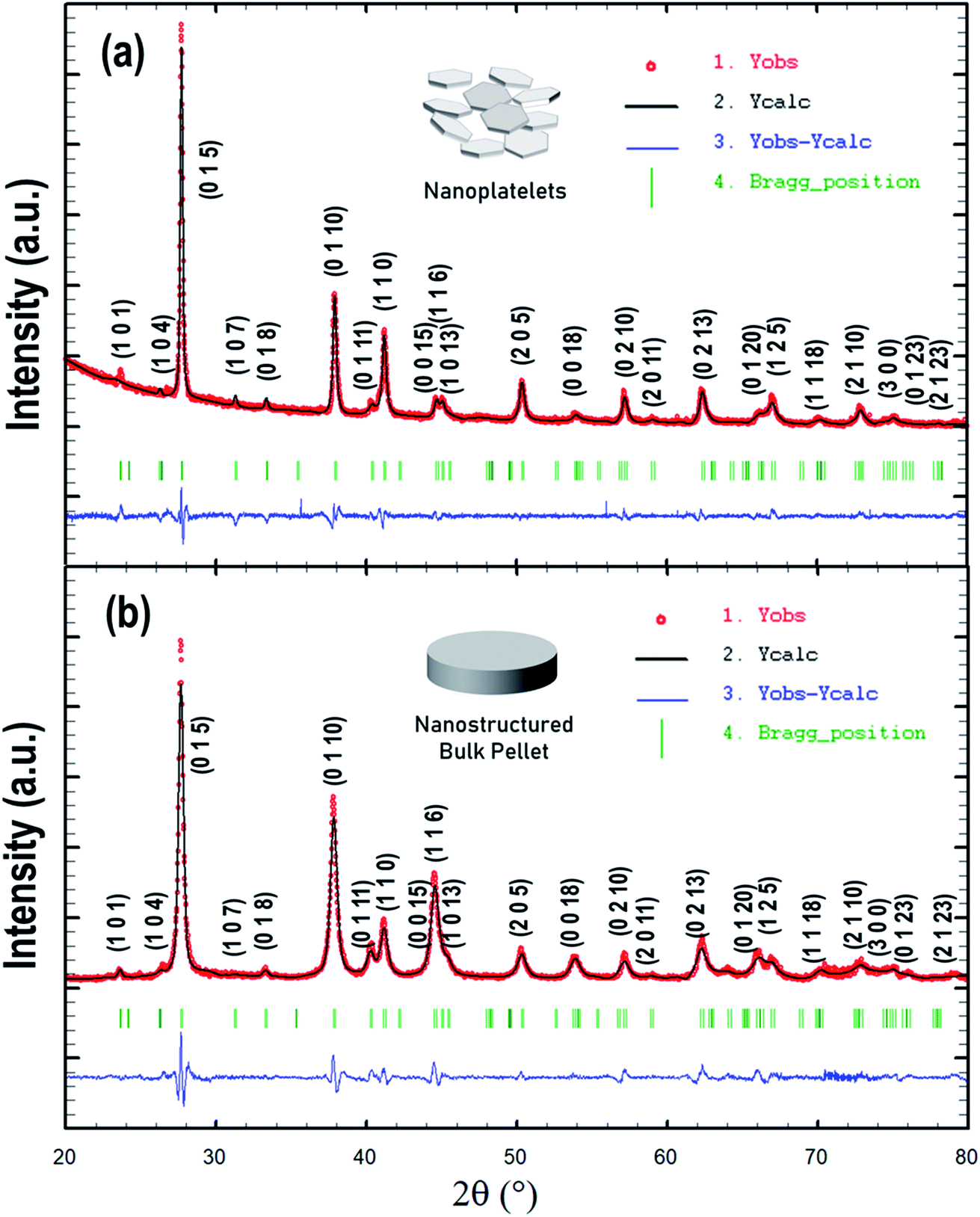 | ||
| Fig. 1 Results of Rietveld refinement of experimental X-ray diffraction patterns for Bi2Te2.7Se0.3 (a) as-synthesized nanocrystals and (b) bulk sintered nanostructured sample. | ||
| R p | R wp | R e | χ 2 | Cell parameters | D avg (nm) | |
|---|---|---|---|---|---|---|
| Bi2Te2.7Se0.3 nanocrystals | 41.0 | 22.9 | 11.10 | 4.24 | a = b = 4.381 Å, c = 30.415 Å | 20 |
| α = β = 90°, γ = 120° | ||||||
| BTS n-type | 14.2 | 16.1 | 8.97 | 3.21 | a = b = 4.385 Å, c = 30.509 Å | 24 |
| α = β = 90°, γ = 120° |
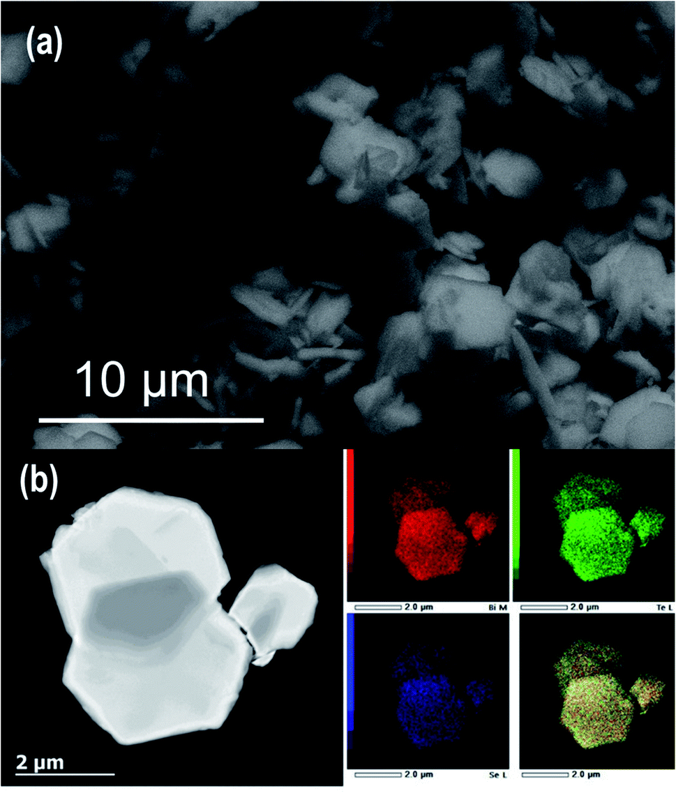 | ||
| Fig. 2 Microstructural characterization of Bi2Te2.7Se0.3 nanocrystals: (a) FE-SEM images; (b) HAADF-STEM image and the corresponding EDX elemental mapping of Bi M, Te L, Se L and overlaid color image. | ||
To gain information about the fine microstructure and the structural arrangement in Bi2Te2.7Se0.3 particles synthesized by colloidal synthesis, we further conducted a HAADF-STEM study in conjunction with SAED analysis. Fig. 3 shows representative high-resolution HAADF-STEM images of the as-synthesized plate-like particle along the [001] and [210] zone axes, together with the respective SAED patterns. One can observe that the sample is highly crystalline and remarkably defect free. The SAED patterns can be completely indexed in the rhombohedral crystal structure using unit cell parameters estimated by Rietveld refinement (Table 1). The overlaid structural models in high-resolution images agree well with experimental observation (Fig. 3), demonstrating the perfect structural arrangement in the resultant hexagonal-shaped plate-like Bi2Te2.7Se0.3 particles.
 | ||
| Fig. 3 HAADF-STEM characterization of Bi2Te2.7Se0.3 nanocrystals for [001] and [210] zones together with enlargement images and structural model overlay (Bi: red, Te/Se: yellow). Insets show corresponding SAED diffraction patterns. | ||
3.2 Dense Bi2Te2.7Se0.3 material formed from plate-like particles by SPS
Having in hand a large quantity of highly crystalline Bi2Te2.7Se0.3 plate-like particles, we next used them to fabricate a bulk TE material via SPS employing rapid heating rates. During the SPS cycle, the passage of high current through powder produces localized heating within the grain boundaries, thereby limiting the grain growth and eliminating porosity. According to the XRD analysis (Fig. 1b), the as-sintered Bi2Te2.7Se0.3 pellet (hereafter referred to as BTS) is a phase-pure material with refined rhombohedral unit cell parameters a = b = 4.385 Å, c = 30.509 Å, α = β = 90°, and γ = 120°, which are quite similar to those of the initial plate-like particles above. The average crystallite sizes of the chemically synthesized Bi2Te2.7Se0.3 particles (≈20 nm) and sintered BTS samples (≈24 nm), quantitatively assessed using XRD data employing the Williamson–Hall method (Table 1), indicate that nominal growth occurred during sintering. The relative density of the obtained disk-shaped pellet was measured to be ≈95%, which is close to the theoretical density. Such a high value may be attributed to an increased interface density within the densely packed microstructure by deterrent grain growth and densification at very fast heating and cooling rates.3.3 Nearly isotropic electrical transport in bulk nanostructured n-type BTS
Next, we aimed to understand the transport properties of the resultant SPS-sintered BTS materials. Despite the wide range of studies on BTS systems, it is not straightforward to directly compare the transport characteristics between the bulk crystalline material and nanostructured samples. The reason for this is that substantial doping of Bi2Te3-based materials results in lattice defects,50–52 which affect the free carrier density and, therefore, transport properties over a wide range.53–55 The reported electric conductivity changes from ∼0.2–0.4 × 10⁵ S m−1 for macroscale crystalline ingots56,57 and up to ∼1.0 × 10⁵ S m−1 for nanostructured samples.30 This is attributed to a higher concentration of defects in the nanostructured material especially at nanoparticle interfaces. Therefore, it is more insightful to compare experimental measurements with the theoretically calculated properties, estimated at the value of chemical potential yielding the same free carrier concentration measured in a particular experiment. This way the effect of different defect concentrations due to different fabrication methods is avoided.Experimentally, the anisotropy in the electrical transport between the ab-plane and the c-axis of single crystalline Bi2Te3 alloys has been widely recognized especially in ingots made by unidirectional crystal growing methods.31,58 Also, Bi2Te3 and its alloys were found to be susceptible to deformation-induced defects, which affects the electrical transport properties.16,19,30 Hence, in the BTS fabricated from plate-like particles, the temperature dependent anisotropy of the electrical transport properties of bulk BTS samples were examined in both the in-plane and cross-plane direction for three subsequent runs, as shown in ESI Fig. S3.† Each measurement scan was carried out only in a heating mode from room temperature to 473 K, which took approx. 2 hours to complete.
The temperature dependent σ shown in Fig. S3(a)† along both directions exhibits degenerate semiconducting behavior and is higher at lower temperature for the in-plane direction. This is similar to observations made previously for crystallographically textured n-type Bi2Te3−xSex and can be ascribed to higher charge carrier mobility along the (a, b) crystal plane than in the c direction.16 The temperature dependent α as shown in Fig. S3(b)† increases with increasing temperature and exhibits negative values of α, for measurements along both directions. The measured α vary marginally for lower temperatures and exhibit higher values along the cross-plane direction. However, at higher temperature, the variation becomes more distinct and can be ascribed to the intrinsic excitation of minority charge carriers, which likewise is stabilized for successive measurement runs.
The anisotropic difference observed in as-synthesized sintered BTS alloys along both in-plane and cross-plane measurements for σ were significantly reduced and for α is distinctively evident after the initial measurement run that can be attributed to partial annealing that occurs at higher temperature measurements, which subsequently relieves the thermal stress and alleviates lattice defects arisen during rapid sintering. These observations are in line with the previously observed annealing effects on the electrical properties of n-type Bi2Te3 for annealing done at 423 K.59 The measured σ and α remain unaffected over temperature excursions for successive runs in the measured temperature range. The thermally stabilized synthesized BTS were found to exhibit weakened anisotropy as observed previously for nanostructured bulk polycrystalline n-type Bi2Te3−xSex.15,30
Due to the disk-shaped sample requirement for thermal diffusivity measurement as shown in Fig. S2(b),† the measurement for thermal transport was done only along the cross-plane direction. Notably, both electrical and thermal characterization in the cross-plane direction for the thermally stabilized sample were analysed and are presented in the subsequent section to marginalise the effect of non-homogeneity and crystallographic orientations introduced during sintering, thus minimizing the possibility of erroneous data.
3.4 Low effective mass and high carrier mobility in n-type BTS
The experimental measurements and theoretical estimations of the temperature-dependent TE transport property of the resultant bulk nanostructured BTS sample are shown in Fig. 4. We first investigated the electrical transport of BTS. The σ displayed in Fig. 4a slightly decreases with increasing temperature, indicating a degenerate semiconducting behaviour. The experimental σ lies between the theoretical estimates for BTS as a result of optimal carrier concentration n ≈ 2.5 ± 0.5 ×1019 cm−3 and high carrier mobility μ ≈ 240 ± 5 cm2 V−1 s−1, which is comparable to previous reports.20,26,60 The theoretical dependence of σ is the result of competing processes of a growing number of charge carriers along with a rapidly decaying electron–phonon relaxation time (Fig. 4a).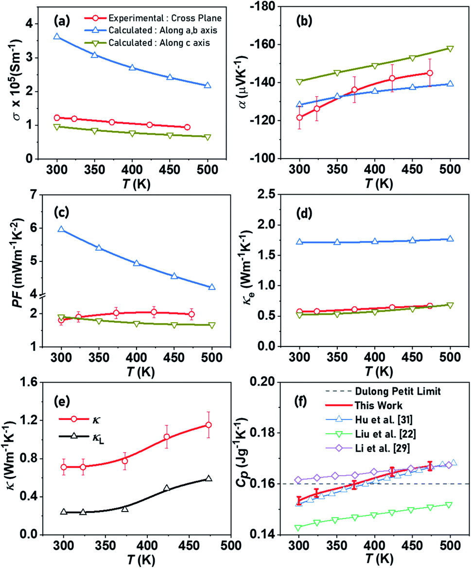 | ||
| Fig. 4 Temperature-dependent transport properties of synthesized Bi2Te2.7Se0.3 nanostructured bulk alloy, BTS (a) electrical conductivity, (b) Seebeck coefficient, (c) power factor, (d) electronic thermal conductivity, (e) total and lattice thermal conductivity, and (f) specific heat capacity.22,29,31 | ||
The plot of α is depicted in Fig. 4b, which exhibits negative values ranging from −120 to −145 μV K−1, indicating that n-type conduction occurs with electrons as the majority charge carriers. It can be observed that α increases with increasing temperature both experimentally and theoretically, which can be associated to the solubility of Se (at Te sites) in Bi2Te3 that creates donor levels in the band gap of Bi2Te3, leading to favourable modification in the electronic density of states (DOS). This inhibits the onset of intrinsic minority carrier conduction in the synthesized BTS at higher temperature, which is in line with the theoretical estimates predicting an increase in α with temperature and within the similar range. The increasing α(T) estimated theoretically accounts for a considerable presence of minority charge carriers in the measured temperature range due to the narrow band gap of Bi2Te3.6 The growth of α measured in this work reflects the strong effect of nanostructuring and band-gap engineering on electronic properties in suppressing the bipolar transport within the measured temperature regime.
To further elucidate the degenerate electrical transport of the synthesized BTS, we estimated the carrier effective mass (m*) based on the energy-independent relaxation time approximation using the Pisarenko relationship between α and n, which is expressed as α = (8π2kB2/3eh2)m*T(π/3n)2/3, wherein kB and h are the Boltzmann constant and Planck constant, respectively. Assuming a single parabolic band, α at any given temperature can be described by a unique value of m*. This value for the SPS-sintered BTS at room temperature was calculated to be 0.52me, where me represents the mass of an electron. Thus, the low m* explains the high μ and lower values of α attained in the prepared BTS material. The cumulative measurement of electrical transport, i.e., power factor (PF, α2σ), revealed a high value, which decreases with increasing temperature (Fig. 4c). The PF lies in the range of 1.8–2.1 mW m−1 K−2, which is closer to theoretical estimates along the c axis and is comparable to previous reports on similar compositions.15–22,29–32 Moreover, on average the experimentally attained PF is higher than the theoretical estimates (along the same axis), which may be ascribed to suppressed bipolar conduction, low m*, and high μ.
3.5 Reduced thermal conductivity in BTS due to grain boundary scattering
The electronic thermal conductivity (Fig. 4d) can be experimentally evaluated according to the Wiedemann–Franz law κe = L × σ × T, where L is the Seebeck-dependent Lorenz number.61 The L values are in the range of (1.7–1.8) × 10−8 W Ω K−2. Similar to theoretical estimates, the experimental κe varies marginally in the measured temperature regimes and is in close agreement with estimates along the c-axis as anticipated for cross-plane measurements. It is evident that the experimentally measured σ and the κe closely follow the theoretical estimates for a macroscale BTS crystal in the direction of the c-axis of the hexagonal lattice, i.e. perpendicular to the plane of easy cleavage and, hence, larger contact area. This is an intriguing observation as it shows that the samples prepared in this work sustain bulk-like electric conductivity, while suppressing lattice thermal conduction.After revealing the electrical transport characteristics of BTS, we then moved forward with probing thermal transport in the TE material. The total thermal conductivity was calculated using the equation κ = D × ρ × Cp. As shown in Fig. 4e, κ is significantly suppressed at lower temperature, which may be ascribed largely to grain boundary scattering by nanostructuring. However, with rising temperature, κ increases due to intrinsic excitation, resulting in the ambipolar diffusion of electron–hole pairs. A minimal κ ≈ 0.7 W m−1 K−1 at 300 K is attained, which is among the lowest reported15–22,29–32 in a polycrystalline n-type Bi2Te3-based composition and can mainly be attributed to the plate-like microstructural features of the constituting particles (Fig. 2).62 The lattice thermal conductivity was calculated using the equation κL = κ − κe and is presented along with κ in Fig. 4e. The κL is significantly suppressed at lower temperature, which can be attributed to grain boundary scattering resulting from bulk nanostructuring in the SPS-sintered BTS.63 The nanosized features specifically target the scattering of low frequency phonons with a long mean free path, as observed in the synthesized bulk nanostructured BTS.
Additionally, alloy scattering supplemented by mass fluctuation due to isoelectronic Se substitution synergistically contribute towards the enhancement of phonon scattering.64 Further reduction in the κL of the synthesized BTS can be achieved using nano-microstructural alteration, doping and disordering by high pressure and high strain deformation.63–65 In the κ estimation particularly at higher temperatures, the uncertainty in the absolute magnitude of Cp measurements of systems, especially those having substantial latent heats (e.g., during phase transitions), often leads to inaccuracy in calculating their κ (≈10% or more).66 Generally, the temperature-independent Dulong–Petit heat capacity provides a close approximation near room temperature, which can be modeled at higher temperatures assuming linear temperature dependence. The temperature-dependent Cp measurement of the synthesized nanostructured BTS sample shown in Fig. 4f is found to be in close proximity to the Dulong–Petit limit and in a similar range as reported previously.22,29,31
3.6 High thermoelectric ZTavg ≈ 0.93 over 300–473 K range
Fig. 5a shows the ZT values as a function of temperature for the SPS-sintered n-type BTS. The material exhibits high ZT near lower temperatures with a ZTmax ≈ 1 at 373 K for the cross-plane direction, which is comparable to the highest ZT in n-type Bi2Te3-based TE materials.15–22,29–32 The low effective mass, high carrier mobility, and relatively low κL boost the TE performance of the as-synthesized n-type Bi2Te2.7Se0.3 alloy to the state-of-the-art level. Furthermore, the ZTavg in the measured temperature range is evaluated using67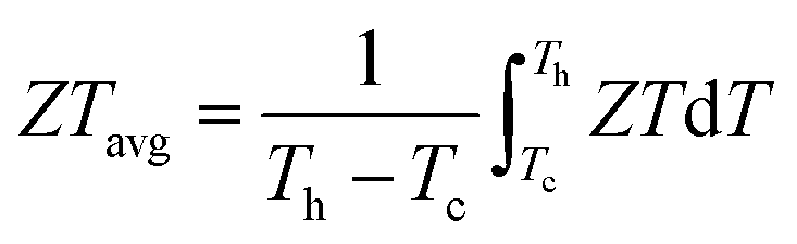
 | ||
| Fig. 5 Temperature-dependent (a) thermoelectric figure of merit (ZT) and (b) thermoelectric compatibility factor (CF), of synthesized Bi2Te2.7Se0.3 bulk nanostructured alloys. | ||
The observed excellent average ZTavg ≈ 0.93 in the low temperature range i.e. 300–473 K is attributed to the synergistic combination of reduced κL and maintained high power factor in the measured temperature range.
In support of the fact that our BTS is a good TE material, we further considered its compatibility factor, which is an important characteristic for real TE device application. Even in the case of high temperature sources, the thermoelements can be segmented by using Bi2Te3-based materials at low temperature ends, since they are the best available TE materials for low temperature applications.6 The efficacy of such segmentation is calculated by the TE compatibility factor68 . The CF of the SPS-sintered n-type BTS nanostructured alloys is shown in Fig. 5b. From an applicability perspective in segmentation, the difference in CF for the two TE materials should be less than a factor of 2. The calculated CF of our TE material decreases with increasing temperature as a result of its direct correlation with ZT, and it is comparable to other state-of-the-art n-type TE materials in the mid-temperature range.69 This result suggests that n-type BTS formed from plate-like particles will also be a suitable TE material for segmentation with high-performance mid-temperature TE materials,22 such as PbTe70 and half-Heuslers,71–74 for achieving efficient TE energy conversion.
4. Discussion
4.1 Correlation of chemical synthesis with high TE performance
The scalable synthesis of phase pure and highly crystalline nanomaterials with homogeneous and controllable chemical composition, size, and shape is a pre-requisite to commercialize the newly developed approaches to production levels. Traditionally, Bi2Te3-based alloys were mainly synthesized employing high-temperature alloying, wherein high purity elemental precursors are co-melted at temperatures above 773 K, and kept for a prolonged period of time at such elevated temperature for homogeneous mixing, followed by gradual cooling. For large-scale commercial applications, zone melting is a commonly used production technology for Bi2Te3-based materials and devices.31 Despite higher power factors achieved in several studies, a proportional increase in κ due to coupling had largely limited efforts aimed towards ZT enhancement.6,16,29,30 Although orienting crystallographic planes by texturing16,75 and deformation31,32,76 were found effective to achieve higher ZT, the anisotropic trends of TE transport due to deformation-induced defects are not well established as higher ZT were achieved both in planes parallel16 and perpendicular30 to the pressing direction.The nanostructuring approaches for κ reduction by random grain orientations and grain size reduction often tend to impede the carrier transport, thereby deteriorating μ in nano-crystalline materials. In principle, ZT could be greatly improved if nanostructured grains were preferentially oriented to achieve κ reduction while maintaining the high power factor. Herein, a novel large-scale chemical alloying synthesis that allows precise substitutional doping has been demonstrated for the synthesis of a bulk nanostructured BTS alloy at a much lower temperature and energy requirement than traditionally used energy-intensive processes such as ball milling20–22,28–30 and melt-spinning.19,27,33,34 This approach combines a colloidal synthesis method and thermal SPS processing under controlled heating conditions under inert atmosphere. Moreover, the uniaxial pressure and optimal sintering conditions assist the favorable orientation of particle domains with limited grain growth. We show that this preparation approach allows the realization of a ca. 5 g batch of Bi2Te3 and its derivatives with nearly stoichiometric chemical doping.
It is widely acknowledged that different synthesis methodology results in distinct physical and transport properties, highlighting the vital role of material processing. The nanostructuring routes that were implemented for bulk TEs mainly comprise two steps: (i) producing nanostructured powders and (ii) their consolidation into bulk by sintering. A comparison of the presented methodology with nanostructuring approaches, such as solvothermal,15 hydrothermal,18 melt-spinning,19 and ball milling,20,30 in the recent literature for pristine Bi2Te2.7Se0.3 bulk nanostructured alloys is summarized in Fig. 6. This comparison suggests that the attained ZT in the measured temperature range is comparable to those obtained through other nanostructuring routes, and can also give rise to the scalable synthesis of high-performance Bi2Te3-based TE materials. Further ZT enhancement is achievable in the synthesized bulk nanostructured BTS by applying hot deformation,31,32,76 liquid state manipulation,16,75 doping (via Cu,52 K,77 and I78 dopants), and nanocomposite (using SnS2,79 GaAs,80 and InSb29 nanoparticles) approaches.
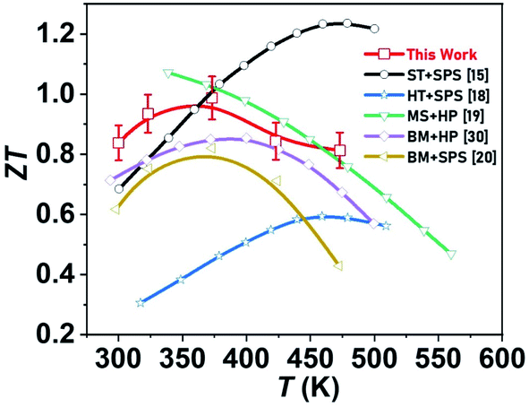 | ||
| Fig. 6 ZT comparison with state-of-the-art of Bi2Te2.7Se0.3 nanostructured bulk alloys synthesized by solvothermal (ST),15 hydrothermal (HT),18 melt-spinning (MS),19 ball-milling (BM),20,30 consolidated employing hot pressing (HP)19,30 and spark plasma sintering (SPS).15,18,20 | ||
4.2 High ZT from high carrier mobility and low frequency phonon scattering
The BTS alloy prepared from the high quality Bi2Te2.7Se0.3 plate-like particles is a solid solution of bismuth telluride with the isomorphous bismuth selenide, which displays high μ with optimal n and reduced κL. Thus, the nanostructure-induced enhanced scattering of phonons in this solid solution does not reduce the μ resulting in high PF and low κ, which synergistically led to favourable thermal and electrical transport for achieving high ZT. The experimentally measured electrical properties exhibit inverse correlation with α and σ with n-type degenerate semiconducting charge transport, in close agreement to the theoretically estimated mixed conduction. The suppressed bipolar conduction and shifting of thermal excitation of minority charge carriers to higher temperature resulted in improved electrical transport that corroborated the theoretical estimates, which does not account for nanostructuring.The ultra-low κL attained in the BTS alloy was mainly attributed to the enhanced grain boundary scattering of low frequency phonons (dominant in near room temperature regimes) by arrays of dislocations at semi-coherent grain boundaries and micro-, sub-micro-, and nano-scale domains in the lattice structure (Fig. 2). Such a microstructure will allow selective scattering of only phonons and will not impact electrons/holes, which have relatively longer wavelengths as indicated by higher μ, thus attaining higher σ (Fig. 4a). Our current data indicate that a combination of large-scale colloidal synthesis of Bi2Te2.7Se0.3 plate-like particles with judicious spark plasma sintering is critical for achieving high ZTmax ≈ 1 (373 K) and remarkable ZTavg ≈ 0.93 (300–473 K). Importantly, these values are among the highest reported for n-type Bi2Te3-based TE alloys.15–22,29–32
5. Conclusion
In summary, we have reported the large-scale colloidal synthesis of hexagonal-shaped plate-like Bi2Te2.7Se0.3 particles. Their detailed characterization revealed the phase purity, high crystallinity, and chemical uniformity of the as-synthesized material. The Bi2Te2.7Se0.3 particles were consolidated into a dense bulk material by time-efficient spark plasma sintering and the resultant n-type thermally stabilized Bi2Te2.7Se0.3 alloy demonstrates high room temperature carrier mobility of ca. 240 cm2 V−1 s−1 at an optimal carrier concentration of ca. 2.5 × 1019 cm−3, achieving a higher average power factor of ≈2 mW m−1 K−2. The micro-, sub-micro-, and nano-scale features of constituent Bi2Te2.7Se0.3 particles were reflected in the ultra-low room temperature total thermal conductivity of ca. 0.7 W m−1 K−1 in the sintered material. Thereby, the as-prepared Bi2Te2.7Se0.3 alloy delivers a high figure of merit ZT ≈ 1 at 373 K with average ZT ≈ 0.93 (300–473 K). The potential of bulk nanostructuring in Bi2Te2.7Se0.3 alloys is corroborated by comparing the experimental outcomes of TE transport with theoretical estimates obtained by ab initio modeling. The enhancement in ZT is primarily ascribed to suppressed bipolar conduction leading to a higher power factor with a simultaneous reduction in lattice thermal conductivity due to the significant grain boundary scattering by bulk nanostructuring.Data availability statement
The data that support the findings of this study are available upon request from the authors.Conflicts of interest
There is no conflict of interest to declare.Acknowledgements
We thank the members of the Nanochemistry Research Group (http://nanochemgroup.org) at INL for insightful discussions and support. This work was supported by Portuguese National Funding Agency for Science, Research and Technology (FCT) under the UT-BORN-PT project (UTAP-EXPL/CTE/0050/2017). B. A. K. acknowledges funding of this work by the Robert A. Welch Foundation (grant no. F-1464). The authors acknowledge the Texas Advanced Computing Center (TACC) at The University of Texas at Austin for providing HPC resources that have contributed to the research results reported within this paper. URL: http://www.tacc.utexas.edu.References
- R. Freer and A. V. Powell, J. Mater. Chem. C, 2020, 8, 441–463 RSC.
- F. J. DiSalvo, Science, 1999, 285, 703–706 CrossRef.
- G. Snyder and E. Toberer, Nat. Mater., 2008, 7, 105–114 CrossRef.
- D. Beretta, N. Neophytou, J. M. Hodges, M. G. Kanatzidis, D. Narducci, M. Martin-Gonzalez, M. Beekman, B. Balke, G. Cerretti and W. Tremel, Mater. Sci. Eng., R, 2019, 138, 100501 CrossRef.
- D. Wright, Nature, 1958, 181, 834 CrossRef.
- H. J. Goldsmid, Materials, 2014, 7, 2577–2592 CrossRef.
- I. Petsagkourakis, K. Tybrandt, X. Crispin, I. Ohkubo, N. Satoh and T. Mori, Sci. Technol. Adv. Mater., 2018, 19, 836–862 CrossRef.
- C. Dagdeviren, Z. Li and Z. L. Wang, Annu. Rev. Biomed. Eng., 2017, 19, 85–108 CrossRef.
- N. Nandihalli, C.-J. Liu and T. Mori, Nano Energy, 2020, 78, 105186 CrossRef.
- Z. Soleimani, S. Zoras, B. Ceranic, S. Shahzad and Y. Cui, Sustainable Energy Technologies and Assessments, 2020, 37, 100604 CrossRef.
- I. T. Witting, T. C. Chasapis, F. Ricci, M. Peters, N. A. Heinz, G. Hautier and G. J. Snyder, Adv. Electron. Mater., 2019, 5, 1800904 CrossRef.
- J. P. Heremans, R. J. Cava and N. Samarth, Nat. Rev. Mater., 2017, 2, 1–21 Search PubMed.
- Y. Liu, Y. Zhang, S. Ortega, M. Ibáñez, K. H. Lim, A. Grau-Carbonell, S. Martí-Sánchez, K. M. Ng, J. Arbiol and M. V. Kovalenko, Nano Lett., 2018, 18, 2557–2563 CrossRef CAS.
- M. Scheele, N. Oeschler, I. Veremchuk, K.-G. Reinsberg, A.-M. Kreuziger, A. Kornowski, J. Broekaert, C. Klinke and H. Weller, ACS Nano, 2010, 4, 4283–4291 CrossRef CAS.
- M. Hong, T. C. Chasapis, Z.-G. Chen, L. Yang, M. G. Kanatzidis, G. J. Snyder and J. Zou, ACS Nano, 2016, 10, 4719–4727 CrossRef CAS.
- Y. Liu, Y. Zhang, K. H. Lim, M. Ibáñez, S. Ortega, M. Li, J. David, S. Martí-Sánchez, K. M. Ng and J. Arbiol, ACS Nano, 2018, 12, 7174–7184 CrossRef CAS.
- A. Soni, Z. Yanyuan, Y. Ligen, M. K. K. Aik, M. S. Dresselhaus and Q. Xiong, Nano Lett., 2012, 12, 1203–1209 CrossRef CAS.
- D. Li, X. Qin, Y. Dou, X. Li, R. Sun, Q. Wang, L. Li, H. Xin, N. Wang and N. Wang, Scr. Mater., 2012, 67, 161–164 CrossRef CAS.
- O. Meroz, N. Elkabets and Y. Gelbstein, ACS Appl. Energy Mater., 2020, 3, 2090–2095 CrossRef CAS.
- S. T. Han, P. Rimal, C. H. Lee, H.-S. Kim, Y. Sohn and S.-J. Hong, Intermetallics, 2016, 78, 42–49 CrossRef CAS.
- Y. Pan, T.-R. Wei, C.-F. Wu and J.-F. Li, J. Mater. Chem. C, 2015, 3, 10583–10589 RSC.
- W. Liu, K. C. Lukas, K. McEnaney, S. Lee, Q. Zhang, C. P. Opeil, G. Chen and Z. Ren, Energy Environ. Sci., 2013, 6, 552–560 RSC.
- L. Hicks and M. S. Dresselhaus, Phys. Rev. B: Condens. Matter Mater. Phys., 1993, 47, 12727 CrossRef CAS.
- V. Akshay, M. Suneesh and M. Vasundhara, Inorg. Chem., 2017, 56, 6264–6274 CrossRef CAS.
- V. Stavila, D. Robinson, M. Hekmaty, R. Nishimoto, D. Medlin, S. Zhu, T. Tritt and P. Sharma, ACS Appl. Mater. Interfaces, 2013, 5, 6678–6686 CrossRef CAS.
- J. S. Son, M. K. Choi, M.-K. Han, K. Park, J.-Y. Kim, S. J. Lim, M. Oh, Y. Kuk, C. Park and S.-J. Kim, Nano Lett., 2012, 12, 640–647 CrossRef CAS.
- S. I. Kim, K. H. Lee, H. A. Mun, H. S. Kim, S. W. Hwang, J. W. Roh, D. J. Yang, W. H. Shin, X. S. Li and Y. H. Lee, Science, 2015, 348, 109–114 CrossRef CAS.
- B. Poudel, Q. Hao, Y. Ma, Y. Lan, A. Minnich, B. Yu, X. Yan, D. Wang, A. Muto and D. Vashaee, Science, 2008, 320, 634–638 CrossRef CAS.
- D. Li, J. Li, J. Li, Y. Wang, J. Zhang, X. Qin, Y. Cao, Y. Li and G. Tang, J. Mater. Chem. A, 2018, 6, 9642–9649 RSC.
- X. Yan, B. Poudel, Y. Ma, W. Liu, G. Joshi, H. Wang, Y. Lan, D. Wang, G. Chen and Z. Ren, Nano Lett., 2010, 10, 3373–3378 CrossRef CAS.
- L. Hu, H. Wu, T. Zhu, C. Fu, J. He, P. Ying and X. Zhao, Adv. Energy Mater., 2015, 5, 1500411 CrossRef.
- L. Hu, T. Zhu, X. Liu and X. Zhao, Adv. Funct. Mater., 2014, 24, 5211–5218 CrossRef.
- Y. Pan, U. Aydemir, J. A. Grovogui, I. T. Witting, R. Hanus, Y. Xu, J. Wu, C. F. Wu, F. H. Sun and H. L. Zhuang, Adv. Mater., 2018, 30, 1802016 CrossRef.
- X. Tang, W. Xie, H. Li, W. Zhao, Q. Zhang and M. Niino, Appl. Phys. Lett., 2007, 90, 012102 CrossRef.
- Z.-Y. Hu, Z.-H. Zhang, X.-W. Cheng, F.-C. Wang, Y.-F. Zhang and S.-L. Li, Mater. Des., 2020, 191, 108662 CrossRef.
- V. Sousa, B. F. Gonçalves, M. Franco, Y. Ziouani, N. González-Ballesteros, M. Fátima Cerqueira, V. Yannello, K. Kovnir, O. I. Lebedev and Y. V. Kolen'ko, Chem. Mater., 2018, 31, 260–267 CrossRef.
- L. Han, S. H. Spangsdorf, N. Nong, L. Hung, Y. Zhang, H. N. Pham, Y. Chen, A. Roch, L. Stepien and N. Pryds, RSC Adv., 2016, 6, 59565–59573 RSC.
- M. Saleemi, M. S. Toprak, S. Li, M. Johnsson and M. Muhammed, J. Mater. Chem., 2012, 22, 725–730 RSC.
- J. M. Soler, E. Artacho, J. D. Gale, A. García, J. Junquera, P. Ordejón and D. Sánchez-Portal, J. Phys.: Condens. Matter, 2002, 14, 2745 CrossRef CAS.
- M. Van Setten, M. Giantomassi, E. Bousquet, M. J. Verstraete, D. R. Hamann, X. Gonze and G.-M. Rignanese, Comput. Phys. Commun., 2018, 226, 39–54 CrossRef CAS.
- P. Rivero, V. M. García-Suárez, D. Pereñiguez, K. Utt, Y. Yang, L. Bellaiche, K. Park, J. Ferrer and S. Barraza-Lopez, Comput. Mater. Sci., 2015, 98, 372–389 CrossRef CAS.
- C. Filippi, C. Umrigar and M. Taut, J. Chem. Phys., 1994, 100, 1290–1296 CrossRef CAS.
- H. J. Monkhorst and J. D. Pack, Phys. Rev. B: Solid State, 1976, 13, 5188 CrossRef.
- L. Fernández-Seivane and J. Ferrer, Phys. Rev. Lett., 2007, 99, 183401 CrossRef.
- J. Dumas, G. Brun, B. Liautard, J. Tedenac and M. Maurin, Thermochim. Acta, 1987, 122, 135–141 CrossRef CAS.
- R. Poloni, J. Iniguez, A. García and E. Canadell, J. Phys.: Condens. Matter, 2010, 22, 415401 CrossRef.
- L. M. Pavlova, Y. I. Shtern and R. E. e. Mironov, High Temp., 2011, 49, 369–379 CrossRef CAS.
- G. K. Madsen, J. Carrete and M. J. Verstraete, Comput. Phys. Commun., 2018, 231, 140–145 CrossRef CAS.
- W. Ibarra-Hernández, M. J. Verstraete and J.-Y. Raty, Phys. Rev. B: Condens. Matter Mater. Phys., 2014, 90, 245204 CrossRef.
- J. Horak, J. Navratil and Z. Starý, J. Phys. Chem. Solids, 1992, 53, 1067–1072 CrossRef CAS.
- P. Lošt'ák, Č. Drašar, D. Bachan, L. Beneš and A. Krejčová, Radiat. Eff. Defects Solids, 2010, 165, 211–215 CrossRef.
- W. S. Liu, Q. Zhang, Y. Lan, S. Chen, X. Yan, Q. Zhang, H. Wang, D. Wang, G. Chen and Z. Ren, Adv. Energy Mater., 2011, 1, 577–587 CrossRef CAS.
- X. Duan and Y. Jiang, Appl. Surf. Sci., 2010, 256, 7365–7370 CrossRef CAS.
- Q. Zhang, T. Fang, F. Liu, A. Li, Y. Wu, T. Zhu and X. Zhao, Chem.–Asian J., 2020, 15, 2775–2792 CrossRef CAS.
- S. J. Kim, H. Choi, Y. Kim, J. H. We, J. S. Shin, H. E. Lee, M.-W. Oh, K. J. Lee and B. J. Cho, Nano Energy, 2017, 31, 258–263 CrossRef CAS.
- D. Perrin, M. Chitroub, S. Scherrer and H. Scherrer, J. Phys. Chem. Solids, 2000, 61, 1687–1691 CrossRef CAS.
- M. Kim, S.-i. Kim, H.-j. Cho, H. Mun, H.-s. Kim, J.-H. Lim, S. W. Kim and K. H. Lee, Scr. Mater., 2019, 167, 120–125 CrossRef CAS.
- X. Hu, C. Jiang, Z. Pan, B. Feng, P. Liu, G. Li and Y. Li, Mater. Res. Express, 2018, 6, 035907 CrossRef.
- L. Zhao, B.-P. Zhang, W. Liu, H. Zhang and J.-F. Li, J. Alloys Compd., 2009, 467, 91–97 CrossRef CAS.
- J. Yang, T. Aizawa, A. Yamamoto and T. Ohta, J. Alloys Compd., 2000, 312, 326–330 CrossRef.
- H.-S. Kim, Z. M. Gibbs, Y. Tang, H. Wang and G. J. Snyder, APL Mater., 2015, 3, 041506 CrossRef.
- D. K. Misra, S. Sumithra, N. S. Chauhan, W. Nolting, P. Poudeu and K. L. Stokes, Mater. Sci. Semicond. Process., 2015, 40, 453–462 CrossRef.
- Z. Liu, J. Mao, T.-H. Liu, G. Chen and Z. Ren, MRS Bull., 2018, 43, 181–186 CrossRef.
- R. Gurunathan, R. Hanus and G. J. Snyder, Mater. Horiz., 2020, 7, 1452–1456 RSC.
- S. Grasso, N. Tsujii, Q. Jiang, J. Khaliq, S. Maruyama, M. Miranda, K. Simpson, T. Mori and M. J. Reece, J. Mater. Chem. C, 2013, 1, 2362–2367 RSC.
- M. T. Agne, P. W. Voorhees and G. J. Snyder, Adv. Mater., 2019, 31, 1902980 CrossRef.
- C. Goupil, Continuum theory and modeling of thermoelectric elements, John Wiley & Sons, 2015 Search PubMed.
- G. J. Snyder and T. S. Ursell, Phys. Rev. Lett., 2003, 91, 148301 CrossRef.
- G. J. Snyder and T. Caillat, MRS Online Proceedings Library Archive, 2003, vol. 793 Search PubMed.
- C. Hadjistassou, E. Kyriakides and J. Georgiou, Energy Convers. Manage., 2013, 66, 165–172 CrossRef CAS.
- N. S. Chauhan, S. Bathula, A. Vishwakarma, R. Bhardwaj, K. K. Johari, B. Gahtori, M. Saravanan and A. Dhar, J. Phys. Chem. Solids, 2018, 123, 105–112 CrossRef CAS.
- Y. Xing, J. Yu, C. Hu, Z. Huang, Q. Qiu, C. Wang, X. Xia, Z. Wang, S. Bai, X. Zhao, L. Chen and T. Zhu, Adv. Energy Mater., 2020, 10, 2000888 CrossRef.
- N. S. Chauhan, S. Bathula, B. Gahtori, S. D. Mahanti, A. Bhattacharya, A. Vishwakarma, R. Bhardwaj, V. N. Singh and A. Dhar, ACS Appl. Mater. Interfaces, 2019, 11, 47830–47836 CrossRef CAS.
- N. S. Chauhan, P. R. Raghuvanshi, K. Tyagi, K. K. Johari, L. Tyagi, B. Gahtori, S. Bathula, A. Bhattacharya, S. D. Mahanti and V. N. Singh, J. Phys. Chem. C, 2020, 124, 8584–8593 CrossRef CAS.
- B. Zhu, Z.-Y. Huang, X.-Y. Wang, Y. Yu, L. Yang, N. Gao, Z.-G. Chen and F.-Q. Zu, Nano Energy, 2017, 42, 8–16 CrossRef CAS.
- R. Zhai, L. Hu, H. Wu, Z. Xu, T.-J. Zhu and X.-B. Zhao, ACS Appl. Mater. Interfaces, 2017, 9, 28577–28585 CrossRef CAS.
- K. Park, K. Ahn, J. Cha, S. Lee, S. I. Chae, S.-P. Cho, S. Ryee, J. Im, J. Lee and S.-D. Park, J. Am. Chem. Soc., 2016, 138, 14458–14468 CrossRef CAS.
- F. Hao, T. Xing, P. Qiu, P. Hu, T. Wei, D. Ren, X. Shi and L. Chen, ACS Appl. Mater. Interfaces, 2018, 10, 21372–21380 CrossRef CAS.
- S. Li, X. Liu, Y. Liu, F. Liu, J. Luo and F. Pan, Nano Energy, 2017, 39, 297–305 CrossRef CAS.
- J. Zhang, H. Ming, D. Li, X. Qin, J. Zhang, L. Huang, C. Song and L. Wang, ACS Appl. Mater. Interfaces, 2020, 12, 37155–37163 CrossRef CAS.
Footnote |
| † Electronic supplementary information (ESI) available. See DOI: 10.1039/d0na00691b |
| This journal is © The Royal Society of Chemistry 2020 |