DOI:
10.1039/D0NA00632G
(Paper)
Nanoscale Adv., 2020,
2, 5450-5460
Bias dependent variability of low-frequency noise in single-layer graphene FETs†
Received
31st July 2020
, Accepted 26th October 2020
First published on 26th October 2020
Abstract
Low-frequency noise (LFN) variability in graphene transistors (GFETs) is for the first time researched in this work under both experimental and theoretical aspects. LFN from an adequate statistical sample of long-channel solution-gated single-layer GFETs is measured in a wide range of operating conditions while a physics-based analytical model is derived that accounts for the bias dependence of LFN variance with remarkable performance. LFN deviations in GFETs stem from the variations of the parameters of the physical mechanisms that generate LFN, which are the number of traps (Ntr) for the carrier number fluctuation effect (ΔN) due to trapping/detrapping process and the Hooge parameter (αH) for the mobility fluctuations effect (Δμ). ΔN accounts for an M-shape of normalized LFN variance versus gate bias with a minimum at the charge neutrality point (CNP) as it was the case for normalized LFN mean value while Δμ contributes only near the CNP for both variance and mean value. Trap statistical nature of the devices under test is experimentally shown to differ from classical Poisson distribution noticed at silicon-oxide devices, and this might be caused both by the electrolyte interface in GFETs under study and by the premature stage of the GFET technology development which could permit external factors to influence the performance. This not fully advanced GFET process growth might also cause pivotal inconsistencies affecting the scaling laws in GFETs of the same process.
Introduction
Nowadays, the limitations on advanced CMOS technologies and the predictions for deceleration of Moore's law, have led both the scientific community and semiconductor industry to turn their attention at the development of emerging technologies based on 2-Dimensional (2D) materials such as graphene.1,2 Graphene's extraordinary characteristics such as carrier mobilities up to 2 × 105 cm2 (V s)−1 and saturation velocities of 4 × 107 cm s−1 have placed graphene transistors (GFET) as a quintessential prospective for future applications.3 Despite the fact that the lack of bandgap in graphene due to its semimetal nature makes single-layer (SL) GFETs unsuitable for digital electronics, there has been an enormous increase of analog and RF circuits designed with GFET technology such as: frequency multipliers,4,5 voltage control6,7 and ring oscillators8 as well as terahertz detectors.9–11 Moreover, GFETs are also widely used and tremendously improve the performance of chemical–biological sensors and optoelectronic devices.12–17
It is not enough for recently developed GFET technologies just to exhibit optimal performance, but they should also be reliable and consistent with CMOS ones since the majority of industry aims to develop new GFET processes based on their pre-existing infrastructures designed for silicon devices.18,19 Variability issues are of outmost importance in advanced semiconductor technologies. Regarding GFETs, the thorough study of such effects is crucial for the transition from immature technologies and prototyped devices mainly fabricated in research labs to large-scale wafer production which will lead to a boost of graphene-based applications and products. There are two sources of variabilities in graphene: (a) environmental effect variabilities such as interface traps and (b) material imperfection variabilities such as edge disorders.18 In this work we focus on low-frequency noise (LFN) variability for SL GFETs mainly derived from interface trap statistics which, according to our knowledge, is for the first time investigated. LFN's contribution to the aforementioned circuits is very crucial as it can be upconverted to deleterious phase noise in such high frequency applications.4–11 In addition, it can affect the sensitivity of sensors12–17 while LFN deviations can also be proved useful for such sensing applications.18
Moreover, LFN examination can provide crucial information as far as the quality of the devices and their interfaces is concerned.20,21
Three main effects are considered responsible for the generation of LFN in semiconductor devices and consequently GFETs; firstly, the carrier number fluctuation mechanism (ΔN), secondly the mobility fluctuation mechanism (Δμ) and finally the series resistance (Rc) contribution (ΔR). ΔN model stems from the trapping/detrapping process at semiconductor devices.22,23 In more detail, a free carrier can be captured by an active trap near the dielectric interface and within a few kT from the Fermi level and then emitted back at the conduction path, and as a result a Random Telegraph Signal (RTS) is generated which corresponds to a Lorentzian Power Spectral Density (PSD). For transistors with channels larger than a few hundred nanometers, the number of active traps is high and consequently the superposition of the generated Lorentzian spectra can result in LFN PSDs inversely proportional to frequency under the condition that the traps are uniformly distributed. This is also known as 1/f noise and was first proposed by McWhorter.24 Minimization of device dimensions in advanced CMOS technology nodes has led both the LFN mean value and variance to be dominated by RTS25–27 but this is not yet the case in GFETs. Δμ model occurs due to fluctuations of the bulk mobility and is described by the empirical Hooge expression28 while ΔR one is caused by Rc contribution especially at high current regimes. Several physics-based models, simpler or more analytical ones, are available in literature describing both LFN mean value29–33 and variance34–40 in CMOS transistors. Most of the LFN variance models focus on its area dependence for short channel CMOS devices where RTS prevail34–37 while bias dependence is also analyzed in some of them.38–40 Characterization and modeling of the standard deviation of the natural logarithm of LFN is also very common in bibliography since LFN deviations follow a log-normal distribution.25,27,35–37,39,40
A lot of research has also been conducted regarding LFN in GFETs41–55 and the findings agree that the same mechanisms (ΔN, Δμ, ΔR) are responsible for the generation of LFN. In fact, it has been shown that the nature of LFN in GFETs strongly relies upon the number of layers of the device.47 In transistors with many layers, volume noise (Δμ) prevails while the fewer the layers the more significant the surface LFN (ΔN) becomes. In this work, SL GFETs are governed by trapping/detrapping mechanism which causes an M-shape gate-bias dependence of output LFN divided by squared drain current (SIDf/ID2), referred to 1 Hz, with a minimum at the charge neutrality point (CNP). Residual charge, which dominates at the CNP, can proportionally increase the LFN minimum. Similarly, non-homogeneous charge density at the channel, caused by a relative high drain voltage, can also increase the LFN minimum.53 Δμ model can also contribute to LFN near the CNP always with a Λ-shape trend even at SL GFETs while ΔR has been observed at higher current regime where Rc is important.53–55 LFN in GFETs can be reduced after electron-beam irradiation49 while the same can be achieved with the usage of substrates such as boron nitride.50,51 A number of models have been proposed to describe the behavior of LFN mean value on GFETs but most of them43,45,46 are based on a simple approximation for ΔN model taken from CMOS devices26,29,31 which introduces an ∼(gm/ID)2 trend of SIDf/ID2 LFN. The latter approach can only be functional under uniform channel conditions.54,55 Recently, a complete physics-based LFN model was proposed53–55 which is valid in all operating regions since it accounts for all non-homogeneities of the device.
While there is a significant number of works regarding LFN mean value modeling in GFETs, no studies are available that deal with LFN variability in these devices even though it is equally significant to its mean value. The large deviations of LFN observed in GFETs, makes it urgent to develop statistical LFN models to investigate the physics behind this variability. In the present work, such an analysis that combines both the experimental characterization of LFN variance data and the derivation of a new physics-based statistical compact model, is proposed for the first time. The proposed model reveals the relation of LFN variability with the deviation of the parameters of the fundamental physical generators of LFN in GFETs (ΔN, Δμ). As it is known from CMOS technology, LFN variance is connected with operating conditions in larger devices,39,40 which is the case for the GFETs under study in the present analysis. The proposed model is based on the recently established chemical-potential based one regarding LFN mean value53 as well as CV–IV behavior.56–58 For more details on the CV–IV–LFN model see ESI A (Fig. S1).† The principal idea for the LFN mean value model calculation was to divide the device channel into microscopic uncorrelated local noise sources. The local noise PSD that originates from each LFN mechanism was then calculated and integrated from source to drain in order to analytically evaluate the contributions from ΔN, Δμ and ΔR LFN; by adding these contributions the total LFN PSD is obtained.33 Similarly, in the present work, the variance is calculated locally for each LFN mechanism by applying fundamental laws of statistics.39,40 Then, the integration along the channel leads to an analytical compact solution with the help of the chemical-potential based model mentioned above. The derived model describes very accurately the experimental data and as in CMOS devices,39,40 ΔN and Δμ variance present a bias dependence similar to their means. Thus, ΔN variance is responsible for an M-shape of total LFN variance centered at the CNP, while Δμ variance is more significant near the CNP. The proposed LFN variance compact model can be easily implemented in Verilog-A and annexed at the chemical-potential based model mentioned above 53–58 and then included in circuit simulators.
Trapping/detrapping mechanism that generate LFN is influenced by some additional factors at the solution-gated (SG)-SL GFETs under study59 resulting in a trap distribution different than Poisson which is the case in silicon-oxide devices.27,35–38 More particularly, trapping/detrapping can occur either near the surface of the polyimide substrate or at the graphene–electrolyte interface where processes of association/dissociation with charged moieties can take place.60–63 In addition, GFET technologies are still in a non-optimal stage and thus, extrinsic traps might be generated during the fabrication process affecting the trap statistics behavior.
Results and discussion
On wafer LFN and IV measurements were conducted at top SG-SL GFETs59 at three different device geometries; (a) W = 100 μm/L = 100 μm, (b) W = 50 μm/L = 50 μm and (c) W = 20 μm/L = 20 μm where W, L are the width and length of the device respectively. Top gate voltage was swept from strong p-type to strong n-type region including the CNP with a step of 5 mV while drain voltage was constant, VDS = 50 mV. Arrays of SG-SL GFETs were fabricated (see Experimental data section for more details on fabrication and measurements procedures) and thus, a significant number of samples were measured for each available geometry in order to have adequate data to characterize LFN statistics. In more detail, the analysis took place at around 48–50 samples from geometry (a), 25–28 samples from geometry (b) and 23–25 samples from geometry (c) after the exclusion of outliers. The reason why the number of samples is not constant for each geometry is that some measurements might behave as outliers in some specific operating conditions but not in the whole range. While ID and SID were measured for 100 top gate voltage values, only 11 of them were chosen for the LFN variability analysis in order to speed up the process. These values were extended from high-to low-current regime both at p- and n-type regions in order to permit the thorough study of the LFN variance at all the operating conditions. The schematic of the device under test is shown in Fig. 1a where the graphene channel, the metal contacts, the SU8 passivation, the electrolyte gate and the reference electrode are shown. Fig. 1b illustrates the average Raman spectrum from 400 points in the W = 20 μm/L = 20 μm GFET area after the transfer of graphene (see Experimental data section). Fig. 1c shows a histogram representing the D/G ratio for each of the measured spectra, indicating the rather low density of defects in the graphene lattice.
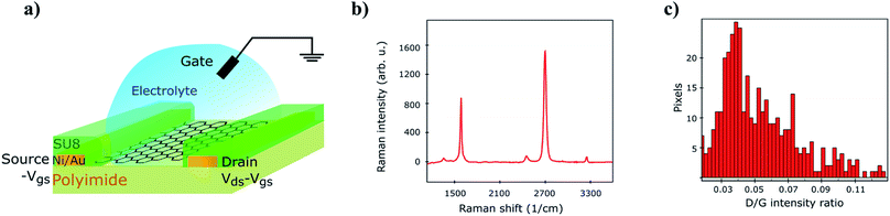 |
| | Fig. 1 (a) Schematic of a SG-SL GFET. (b) Average Raman spectrum over the whole graphene channel and (c) histogram of D/G ratio representative of the defects density distribution. | |
IV model validation
The first step towards the modeling of LFN mean and variance is the extraction of physical parameters related to their stationary response. In Fig. 2a, IV model is validated56–58 for the three GFET geometries under test. The transfer characteristics (drain-source current IDvs. effective gate voltage VGEFF) are shown for all regimes of operation, near and away the CNP, with VGEFF calculated as the gate voltage (VG) minus the voltage at the CNP (VCNP). Fig. 2a also presents the fitting from the chemical-potential based model,56–58 showing a close match with the experimental data. The fundamental parameters of the IV model such as mobility μ, top gate capacitance Ctop, flat band voltage VGSO, residual charge ρ0 and contact resistance Rc are extracted and presented in Table 1. Derived parameters from every GFET are very close, apart from μ and VGSO which are quite heightened for the larger device, which is indicative of the elevated ID data observed there. Also, Rc for the medium sized device is a little decreased.
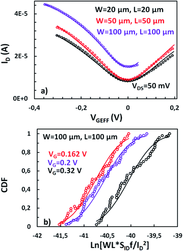 |
| | Fig. 2 (a) Drain current IDvs. top gate voltage overdrive VGEFF, for GFETs with W/L = 20 μm/20 μm, 50 μm/50 μm and 100 μm/100 μm. Markers: measured data, solid lines: model. (b) Cumulative distribution function (CDF) of natural logarithm of normalized LFN ln(WLSIDf/ID2), referred to 1 Hz, for GFET with W/L = 100 μm/100 μm, shows a log-normal distribution. Markers: extracted CDF, solid lines: theoretical CDF of normal distribution of ln(WLSIDf/ID2). | |
Table 1
IV–LFN (mean value–variance) model parameters
| Parameter |
Units |
W/L = 20 μm/20 μm |
W/L = 50 μm/50 μm |
W/L = 100 μm/100 μm |
|
μ
|
cm2 (V s)−1 |
3500 |
3800 |
7000 |
|
C
top
|
μF cm−2 |
2 |
2 |
2 |
|
V
GSO
|
V |
0.278 |
0277 |
0.33 |
|
ρ
0
|
cm−2 |
3.29 × 10¹¹ |
3.29 × 10¹¹ |
3.43 × 10¹¹ |
|
R
c
|
Ω |
400 |
320 |
380 |
|
N
T
|
eV−1 cm−3 |
2.2 × 10¹⁹ |
4.93 × 10¹⁹ |
1.74 × 10²⁰ |
|
α
H
|
— |
5.6 × 10⁻⁴ |
1.5 × 10⁻³ |
1.12 × 10⁻² |
|
S
ΔR
2
|
Ω2 Hz−1 |
3 × 10⁻⁴ |
4 × 10⁻⁵ |
1.8 × 10⁻⁵ |
|
N
tcoeff
|
— |
2.7 × 10³ |
2.5 × 10⁵ |
3.4 × 10⁶ |
|
N
α
H
|
— |
1.19 × 10¹³ |
3.5 × 10¹¹ |
3.6 × 10¹⁰ |
LFN mean value model
As described before, ΔN, Δμ, ΔR are the main generators of LFN in GFETs. Regarding LFN variance, the first two are going to be investigated in this work. LFN normalized by the area over squared drain current (WLSIDf/ID2), at 1 Hz, is widely used in literature for the study of LFN variance. The reason for using this normalization is that the variance of this term presents a ∼1/(WL) dependence.35,36,39,40 In Fig. 2b, this form of depiction of LFN data is shown to follow a log-normal distribution (σ[ln(LFN)] = √ln(1 + Var(LFN)/E2(LFN)), where σ is the standard deviation and E the mean value37,40) for the first time in GFETs. Cumulative distribution function (CDF) of the natural logarithm of WLSIDf/ID2 for the 100 μm/100 μm GFET is presented at three different VGEFF; markers present the extracted CDF of the random variable X = ln[WLSIDf/ID2] while the solid lines the theoretical CDF under the consideration that X is normally distributed. The precise fitting among markers and lines confirms that WLSIDf/ID2 data indeed follow a log-normal distribution. Fig. 3a and b indicate the correlation of the WLSIDf/ID2 variability with VGEFF (or VCNP equivalently) and ID variabilities, respectively for the same device. It is evident that this correlation is very weak, and this observation proves that LFN variance is not related to the variability of the IV characteristics but is mostly due to trap statistics as well as Hooge parameter variations as it will be shown later. See ESI B (Fig. S2)† for the equivalent plots as Fig. 2b and 3a for the rest of the GFET areas. Therefore, for the derivation of the LFN variance model, it is crucial to first determine the parameters of the LFN mean value model that are sensitive to variations. These are the number of traps Ntr from ΔN effect and Hooge parameter αH from Δμ one. Fluctuations of the two aforementioned parameters from sample to sample lead to different LFN magnitudes and consequently cause LFN variance. Thus, the only way to explicitly model this variance is to examine how the deviation of these parameters affect the statistical behavior of the two mechanisms that generate LFN. The WLSIDf/ID2 PSD locally in the device's channel for a slice Δx, for both mechanisms, is given by:53| | 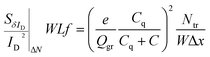 | (1) |
| |  | (2) |
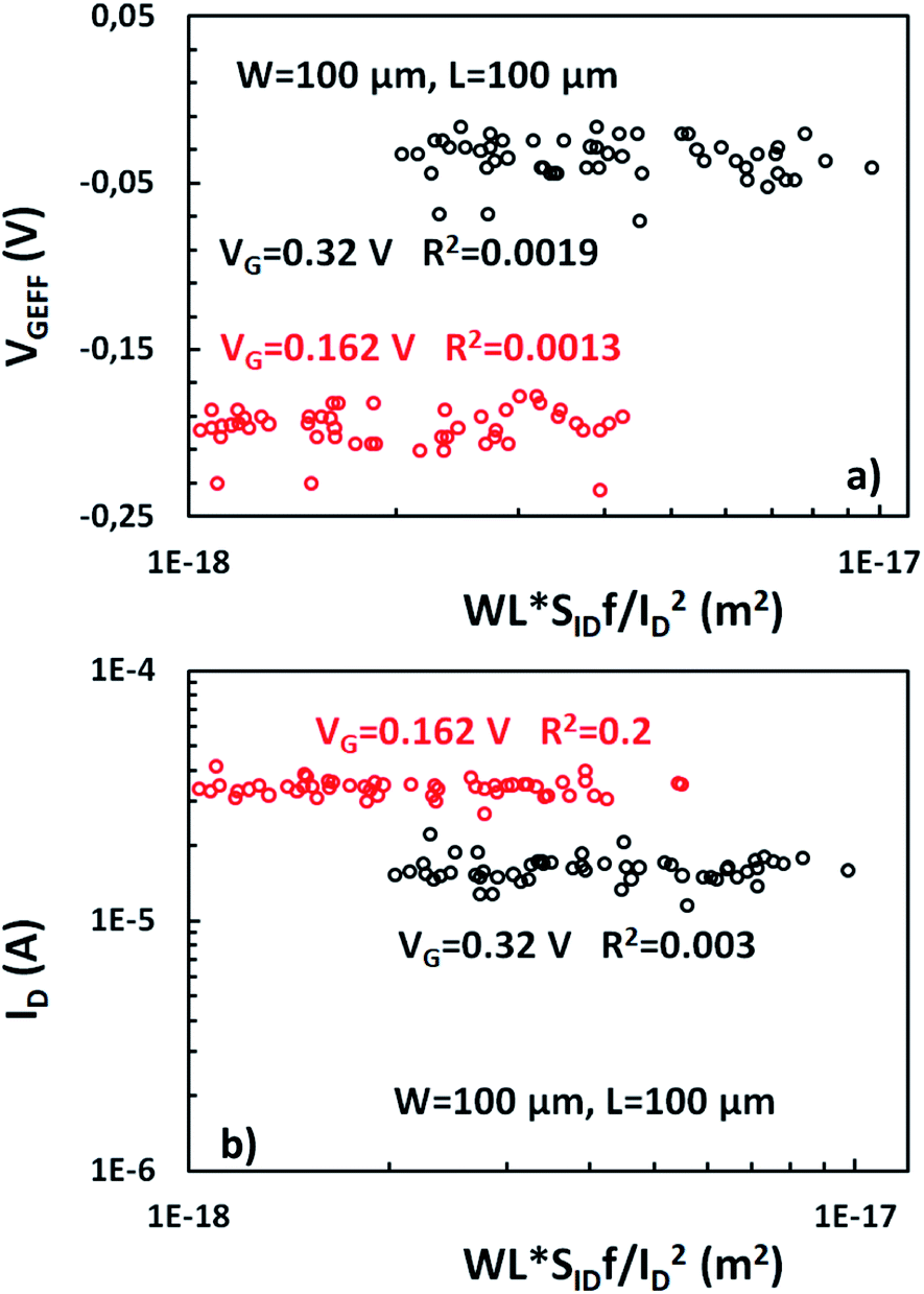
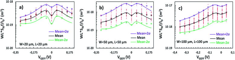
respectively, where Ntr = WLNt = KTλNT31,32 is the number of active traps, Nt is the trap density in (cm−2) and NT is the volumetric trap density in (eV−1 cm−3) which is used as a LFN mean value model parameter.53K is the Boltzman constant, T is the absolute temperature, λ ≈ 0.1 nm is the tunneling attenuation distance, e is the electron charge, Qgr is the graphene charge stored in the quantum capacitance Cq, C = Ctop + Cback is the sum of top and back interface capacitances, αH is the unitless Hooge parameter which is also used as a LFN mean value model parameter53 and f is the frequency. See ESI A (Fig. S1)† for more details on the definition of different quantities. To obtain the total LFN PSDs, integration of the local PSDs derived above with an integral variable change from length x to chemical potential Vc should take place.53–55 The SG-SL GFETs which are examined in this study are long-channel devices operating at low electric field region due to small drain voltage and thus, Velocity Saturation (VS) effect54 is not expected to contribute to LFN variance. Consequently, VS effect is ignored in the derivation of the model that follows in order to keep the expressions simple. The complete model including VS contribution to LFN variance is presented in ESI C (see eqn (S6)–(S12), Fig. S3).† It is confirmed that VS is negligible under low electric field conditions while it can increase variance at high electric fields. LFN mean value model is validated with experimental data, averaged in a bandwidth 1–30 Hz, in Fig. 4 for all the GFETs under test. WLSIDf/ID2 ln-mean data with black circular markers and LFN mean value model53 with solid black lines are shown for the W/L = 20 μm/20 μm GFET in Fig. 4a, for the W/L = 50 μm/50 μm GFET in Fig. 4b and for the W/L = 100 μm/100 μm GFET in Fig. 4cvs. VGEFF with very consistent results for all the devices and for all regions of operation. The logarithmic (ln)-mean values are used for better accuracy due to log-normal distribution of LFN. The LFN data for the total of the measured samples are also shown with smaller red markers. Δμ model is significant near the CNP and from there the αH parameter can be extracted, ΔN LFN is responsible for the M-shape of WLSIDf/ID2 and thus, NT parameter can be extracted from fitting the ΔN model of LFN generation. Finally, the contribution from ΔR can be identified at higher gate voltage values, where SΔR2 can be extracted.55 The LFN mean value model parameters are presented in Table 1. NT and αH increase with the area of the GFETs, with the greatest increment observed in the largest devices (W/L = 100 μm/100 μm), where they double with respect to the medium sized devices (W/L = 50 μm/50 μm). Oppositely, SΔR2 reduces with the GFET channel area. The reason for this deviation of LFN mean value parameters is not well understood but GFET technologies are not as mature as CMOS for example, and this might cause such deviations even for parameters of the same technology. The ensuing LFN statistical analysis will confirm that ΔN and Δμ models define LFN variance similarly as its mean value.
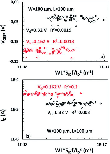 |
| | Fig. 3 (a) Variability of WLSIDf/ID2, referred to 1 Hz, is much higher and uncorrelated with variability of (a) VGEFF and (b) ID for GFET with W/L = 100 μm/100 μm. | |
 |
| | Fig. 4 Normalized LFN WLSIDf/ID2, referred to 1 Hz, vs. top gate voltage overdrive VGEFF, for GFETs with (a) W/L = 20 μm/20 μm, (b) 50 μm/50 μm and (c) 100 μm/100 μm. Measured noise from all available samples: star markers, measured ln-mean noise and its ±2-sigma deviation: open circle markers, mean and ±2-sigma deviation model: lines (mean data and model: black, +2-sigma deviation data and model: purple, −2-sigma deviation data and model: green). | |
LFN variance model
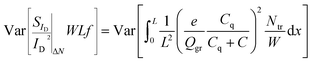
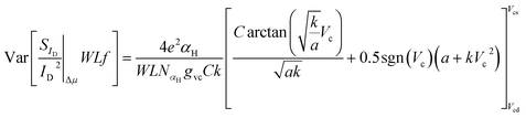
Variations in the number of active traps (Ntr) can definitely induce variations in the ΔN contribution to LFN. Similarly, variations in the αH parameter can produce variability in the effect of Δμ on LFN. In this section, an analytical LFN variance model for each of the two LFN generation mechanisms will be derived. First, LFN variance will be calculated locally in the channel and since the local noise sources are considered uncorrelated,33,53 integration from source to drain can provide the total LFN variance by adding all the local contributions. Estimating variance locally ensures that each ΔID/ID deviation caused by a fluctuation (such as a specific trap) at any infinitesimal area will contribute independently.25,37,39,40 Local variance represents the relative variation induced by each local noise source. Oppositely, only under uniform channel conditions where local variance would be equal throughout the whole channel, it could be taken out of the integral. But this is not the case in this work since all non-homogeneities are taken into account in order to implement a complete model. Fundamental statistics theory gives:| |  | (3) |
where in this study y = Ntr, αH for ΔN, Δμ models respectively and f(Ntr, αH) = Λ(x) (Ntr, αH).
ΔN LFN variance
The total WLSIDf/ID2 ΔN is calculated by integrating eqn (1) along the channel:33,53| | 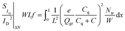 | (4) |
To calculate the variance of eqn (4):
| |  | (5) |
It can be easily proved that since the local noise sources are uncorrelated and thus independent, the following expression is valid:
| | 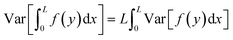 | (6) |
See ESI D† for the mathematical proof of eqn (6). Because of eqn (3) and (6), variance of eqn (5) can enter the integral as:
| | 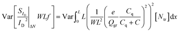 | (7) |
where the quantity inside the integral corresponds to the local variance. In silicon-oxide devices number of traps are known to follow Poisson distribution
27,35–38 which means that its variance equals to its mean value, Var[
Ntr] =
Ntr =
WLKTλNT. It will be shown later that this is not the case in SG-SL GFETs of this work but it rather is Var[
Ntr] =
NtcoeffWLKTλNT, where
Ntcoeff is used as a fitting LFN variance model parameter. According to the latter and if the integral variable is changed from
x to
Vc:
53–58| |  | (8) |
and if
eqn (8) is solved analytically,
eqn (9) is derived.
| | 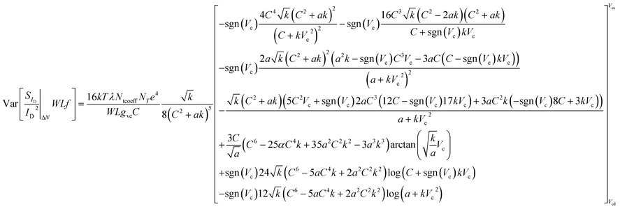 | (9) |
gvc is a normalized drain current term,
53–58α = 2
ρ0e is a residual charge related expression
55–58 and
k is a coefficient.
53–58 For more details on definitions see ESI A.
†eqn (9) predicts an inversely proportional relation of the
WLSIDf/
ID2 Δ
N variance model to the area of the device ∼1/(
WL).
Δμ LFN variance
Following a procedure similar as in ΔN case, the total WLSIDf/ID2 Δμ variance is calculated by integrating eqn (2) along the channel:33,53| | 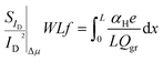 | (10) |
Variance of eqn (10) is calculated after taking into consideration eqn (3) and (6) as in ΔN case since local noise sources are uncorrelated:
| | 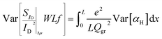 | (11) |
No information is available on literature regarding Var[αH] and thus, in order to achieve a similar scaling with ΔN WLSIDf/ID LFN variance model ∼1/(WL), the following is assumed: Var[αH] = αH(NαHWL)−1 where NαH is a specific density used as a fitting LFN variance model parameter. According to the latter and if the integral variable is changed from x to Vc:53–58
| | 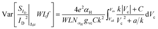 | (12) |
and if
eqn (12) is solved analytically:
| |  | (13) |
Total LFN variance
The total WLSIDf/ID2 variance can be calculated as:| | 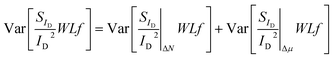 | (14) |
under the approximation that ΔN and Δμ models are uncorrelated. Even though this is not completely accurate, there are distinguished regions where each of these effects is dominant (Δμ at the CNP and ΔN at the peaks of M-shape dependence) and thus the aforementioned independency can be assumed without significant error. Eqn (9), (13) and (14) formulate the new compact statistical LFN model. As shown before, WLSIDf/ID2 follows a log-normal distribution as it can be observed by the CDFs illustrated in Fig. 2b and in ESI B (Fig. S2a and b).† the fundamental expression for this distribution is:37,39| |  | (15) |
where σ(ln[WLSIDf/ID2]) is the standard deviation of the natural logarithm of WLSIDf/ID2 widely used in bibliography,25,27,35–37,39,40E denotes the LFN mean value model and the ratio of variance with squared mean WLSIDf/ID2 is defined as normalized variance.25,27,35–37,39,40 The model in eqn (15) follows the scaling dependence of ref. 37, which is ∼√ln[1 + K/(WL)] and for larger devices turns to ∼√1/(WL) where K/(WL) is the normalized variance established before.37
Experimental validation of the LFN variance model
The qualitative performance of the new derived LFN variance model is verified with the data from SG-SL GFETs under test, as it will be illustrated in the rest of this section. Initially, as it was mentioned before, ln-mean of WLSIDf/ID2 data is calculated for every device under test from all the available samples and used in the verification of the LFN mean value model as in Fig. 4. Afterwards, standard deviation σ(ln[WLSIDf/ID2]) data can be easily extracted from the natural logarithms of all the WLSIDf/ID2 samples again for each available GFET. This process is followed for the derivation of σ(ln[WLSIDf/ID2]) instead of eqn (15) since noise measurements are very sensitive and thus the calculation of normalized variance ratio Var[WLSIDf/ID2]/E2[WLSIDf/ID2] contained in eqn (15) is not very consistent because of the small numbers both in numerator and denominator. Then, WLSIDf/ID2 variance can be estimated through eqn (15) since σ(ln[WLSIDf/ID2]) is already known, by using the ln-mean in the denominator of normalized variance. In Fig. 4, ±2σ standard deviation of WLSIDf/ID2 (σ = √Var) is also shown both for the model and experimental data with purple (+2σ) and green (−2σ) solid lines and markers respectively. The model captures accurately the dispersion of the data and its bias dependence, confirming the consistency between LFN mean value and variance models for all the three GFETs examined.
WLS
I
D
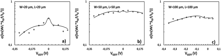
f/ID2 variance and σ(ln[WLSIDf/ID2]) are depicted in Fig. 5 and 6 respectively for the W/L = 20 μm/20 μm GFET in Fig. 5a and 6a, for the W/L = 50 μm/50 μm GFET in Fig. 5b and 6b and for the W/L = 100 μm/100 μm GFET in Fig. 5c and 6cvs. VGEFF. Experimental data are represented with markers while the total model with solid lines. Dashed and dotted lines in Fig. 5 stand for the ΔN and Δμ variance contributions, respectively. This representation confirms that the model precisely captures the experimental data for both WLSIDf/ID2 variance and σ(ln[WLSIDf/ID2]) in the whole range of operation for every GFET under investigation.
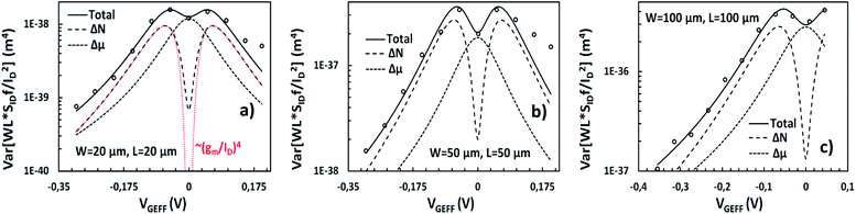 |
| | Fig. 5 Variance of normalized LFN Var[WLSIDf/ID2], referred to 1 Hz, vs. top gate voltage overdrive VGEFF, for GFETs with (a) W/L = 20 μm/20 μm, (b) 50 μm/50 μm and (c) 100 μm/100 μm. Markers: measured data, solid lines: total model, dashed lines: individual contributions (ΔN, Δμ). Simplified LFN variance model ∼(gm/ID)4 which considers a homogeneous channel is shown with red dashed lines for W/L = 20 μm/20 μm GFET (a) for comparison reasons. | |
 |
| | Fig. 6 Standard deviation of natural logarithm of normalized LFN σ[ln(WLSIDf/ID2)], referred to 1 Hz, vs. top gate voltage overdrive VGEFF, for GFETs with (a) W/L = 20 μm/20 μm, (b) 50 μm/50 μm and (c) 100 μm/100 μm. Markers: measured data, solid lines: total model. | |
The ΔN and Δμ models shown in Fig. 5 prove that these effects act similarly as in the LFN mean value model, ΔN effect is responsible for the M-shape of WLSIDf/ID2 variance as it was for the WLSIDf/ID2 mean value while Δμ contributes near the CNP as it did for the LFN mean value model while it retains its Λ shape trend. The new LFN variance model shows a deviation from the experimental data at high n-type conduction regime probably due to ΔR contribution which is not included in this study. For comparison reasons, a LFN variance model based on ∼(gm/ID)2 approximation which considers a uniform channel,26,29,31 is shown in Fig. 5a with red dashed line. This approach estimates an ∼(gm/ID)4 dependence of LFN variance. For the analysis of the derivation of this expression see ESI E.† As it was expected, it gives acceptable results away from the CNP but it is incapable of capturing LFN variance near the CNP where the non-homogeneity of the device is more intense even for small VDS values.53 These non-homogeneities can be easily detected from the illustration of the ΔN LFN contribution to WLSIDf/ID2 variance throughout the channel where, for VGEFF values away from the CNP, local variance is constant along the channel. Oppositely, near the CNP a steep dip is noticed in the middle of the channel in which the exact CNP is located under low VDS. For the above observations see ESI F (Fig. S4).† The experimental data were measured at VDS = 50 mV, but it is quite certain that the inconsistency of the ∼(gm/ID)4 term would be more significant for higher VDS values.
N
tcoeff, NαH parameters of ΔN and Δμ effects respectively, are extracted and shown in Table 1. NαH is calculated from the CNP while Ntcoeff is then adjusted to fit the M-shape. It is clear that Ntcoeff values for all GFETs are far from unity which means that Ntr does not follow a Poisson distribution as in silicon-oxide devices. As stated before, this might be both due to the nature of the traps generated in graphene–electrolyte interface43,60–63 and because of process-induced extrinsic traps of the specific SG-SL GFETs. In order to prove the validity of the obtained Ntcoeff, NαH values, a thorough analysis was conducted where the LFN mean value model parameters (NT–Ntr, αH) were extracted for each of the measured samples for all available GFET areas. The variance of these parameters as well as their ln-mean value were then estimated, allowing to derive the LFN variance model parameters Ntcoeff, NαH, given that Var[Ntr] = NtcoeffWLKTλNT and Var[αH] = αH(NαHWL)−1. These values are proven to be identical with the ones extracted from Fig. 5 and shown in Table 1, which provide the best possible fitting of the model. This result confirms that charge traps do not present a Poisson distribution in the GFETs under study. For the complete analysis see ESI G (Fig. S5 and Table S1).† As it was mentioned before, WLSIDf/ID2 mean value increases as the area gets larger and as a result NT, αH get also higher as shown in Table 1. Table S1† clearly demonstrates that variances of Ntr, αH respectively, increase more strongly than their mean values as the devices' area increases. The latter can justify the boost of Ntcoeff parameter and the reduction of NαH as the dimensions get larger. The reason for these variations of the statistical LFN model parameters which occur as a physical consequence of the variations of the LFN mean value model ones, could be the critical inhomogeneities of GFET technologies, as it has already been stated before.
Standard deviation of natural logarithm σ(ln[WLSIDf/ID2]) of normalized LFN is shown in Fig. 6 and some remarkable conclusions can be extracted. The above quantity can be used as a figure of merit for LFN variability comparisons between the GFET technology in this work and CMOS ones35–37,40 It can be concluded that the range of values between 0.1–1 for all the transistors under test as depicted in Fig. 6 are similar with the results obtained from CMOS devices with similar dimensions, indicating a decent performance for the GFETs under study.35–37,40 Another crucial observation is the weak bias dependence of σ(ln[WLSIDf/ID2]) data with a rather smooth fluctuation near the CNP and a slight decrease away from the CNP, which is remarkably captured by the proposed model.
Despite the fact that the proposed WLSIDf/ID2 variance model focuses on the bias dependence, its scaling with the area is also crucial. ΔN and Δμ WLSIDf/ID2 variance models follow a ∼1/(WL) trend as it is clear from eqn (9) and (13) and as a result total LFN variance expression in eqn (14) behaves similarly. SIDf/ID2 mean value model presents the same dependency.53–55 In addition, σ(ln[WLSIDf/ID2]) also follows an ∼√1/(WL) trend due to the large device dimensions.25,27,35–37,40 However, due to inhomogeneities of the GFET technologies in general, extracted parameters both of the LFN mean value (NT, αH) and variance (Ntcoeff, NαH) models, differ from device to device.
Conclusions
This work investigates thoroughly the bias dependence of LFN variability in large area SG-SL GFETs. To our knowledge, this is the first time that such a study that combines both the analysis of statistical LFN data for graphene devices and the extraction of a physics-based LFN variance model is presented. More specifically, an analytical compact model based on carrier number ΔN and mobility fluctuation Δμ effects has been proposed and implemented for circuit simulators. The development of such an effective tool is critical for the boost of graphene circuit design, where LFN variability should be accurately predicted to prevent performance deterioration in certain applications. The latter is one of the most significant novelties of this work. Besides, it is experimentally proven that LFN variability does not count on the variability of IV quantities such as VCNP, ID but it is directly linked to the number of traps Ntr and Hooge parameter αH variations regarding ΔN and Δμ mechanisms respectively. The derived compact model precisely covers the measured LFN variance over the whole range of operation, from strong conduction to the CNP at both p- and n-type regimes. ΔN and Δμ LFN variance models exhibit a similar bias dependence with the corresponding ΔN and Δμ mean value ones. Thus, ΔN effect accounts for the M-shape of LFN variance similarly as it is known to cause an M-shape for its mean value while Δμ provides a Λ-shape in the bias dependence of LFN variance, which contributes significantly at the CNP, analogously to the Δμ contribution to LFN mean value. It is also worth mentioning that variances of both ΔN and Δμ mechanisms must be computed locally in the channel in order to guarantee that each parameter's (Ntr, αH) deviation at any position in the channel will have an individual impact on LFN variability. A simpler variance model with a ∼(gm/ID)4 shape is also extracted based on a uniform channel approximation and shown for comparison reasons. This approach based on the well-known ∼(gm/ID)2 model of the ΔN contribution to LFN mean value fails to accurately predict the LFN variance near the CNP.
N
T, (or Ntr consequently) and αH parameters of the LFN model mean value are also used in LFN variance model together with the newly defined Ntcoeff and NαH parameters which are extracted from statistical LFN data. In silicon-oxide transistors, Ntr follows a Poisson distribution and thus, Ntcoeff is close to unity but this is not the case in the devices under test. The latter is experimentally shown by extracting LFN mean value model parameters for every measured sample and then by calculating their variance and mean value.
Regarding geometrical scaling, while both SIDf/ID2 mean value and WLSIDf/ID2 variance models predict a ∼1/(WL) behavior, the corresponding data do not follow this trend. In fact, the extracted LFN parameters are not identical for the three GFETs under test despite the fact that they are devices of the same technology. On the contrary, LFN mean value parameters increase with device area causing also a large deviation in LFN variance parameters. This device to device parameters' deviation could be justified due to increased inhomogeneities observed on recently developed GFET technologies.
Eqn (15) expresses the standard deviation of natural logarithm of WLSIDf/ID2 – σ(ln[WLSIDf/ID2]) – which is taken into consideration and examined due to log-normal distribution of LFN data and it might be a reliable tool in order to compare LFN variance for different types of transistors. This study represents the first reported efforts to understand LFN variability in GFETs. The derived results contribute to the thorough understanding of the nature of charge traps statistics in solution-gated devices and they also provide the tools to quantify and predict LFN variability in SL GFETs. This framework is considered critical for upscaling the production of graphene electronics from research labs into larger-scale dedicated fabrication facilities.
Experimental data
Electrical characterization of LFN
To measure the DC transfer curves and the LFN spectra accurately, the drain to source current was pre-amplified in a first amplification stage with a gain of 104. The signal was then high pass filtered, thus canceling its low frequency (i.e. DC level) components. The resulting signal was further amplified and low pass (anti-aliasing) filtered in a second stage with a 102 gain. The signals were digitalized using a NI DAQ Card in all characterization procedures. To extract the power spectral density, the drain to source current was measured under different gate bias conditions for 10 s at each point.
Fabrication of SG GFETs
Arrays of SG-SL GFETs were fabricated on a 10 μm thick polyimide (PI-2611, HD MicroSystems) film spin coated on a Si/SiO2 4′′ wafer and baked at 350 °C. A first metal layer (10 nm Ti/100 nm Au) was deposited by electron-beam vapour and then structured by a lift-off process. Afterwards, the graphene grown by chemical vapour deposition on Cu was transferred (process done by Graphenea s.a.). Graphene was then patterned by oxygen plasma (50 sccm, 300 W for 1 min) in a reactive ion etching (RIE) after protecting the graphene in the channel region with HIPR 6512 (FujiFilm) positive photoresist. After the graphene etching, a second metal layer was patterned on the contacts following the same procedure as for the first layer. The lift-off was followed by an annealing in ultra-high vacuum consisting on a temperature ramp from room temperature to 300 °C. Subsequently, the transistors were insulated with a 3 μm-thick photodefinable SU-8 epoxy photoresist (SU-8 2005 Microchem), keeping uncovered the active area of the transistors channel and the contacting pads. The polyimide substrate was structured in a reactive ion etching process using a thick AZ9260 positive photoresist (Clariant) layer as an etching mask. The neural probes were then peeled off from the wafer and placed in a zero-insertion force connector to be interfaced with our custom electronic instrumentation. Finally, the devices were rinsed for 2 minutes in ethanol to eliminate remaining resist residues on the graphene channel.
Raman characterization of graphene after transfer
A SLG sample was transfer onto a SiO2 wafer following the same process as detailed for the fabrication of GFETs. The Raman spectra at 400 equally spaced points were acquired on the graphene sample, within an area of 20 μm × 20 μm. A Witec spectrometer in backscattering configuration, using a 600 gr per nm grating was used. A 488 nm wavelength laser (2.5 mW power) was focused on the sample with a 50× objective. The peak intensity for the D and G bands was measured after background subtraction.
Data availability
The data that support the findings of this study are available from Ramon Garcia Cortadella. Please, address your requests to E-mail: ramon.garcia@icn2.cat.
Conflicts of interest
There are no conflicts to declare.
Acknowledgements
This work was funded by the European Union's Horizon 2020 research and innovation program under Grant Agreement No. GrapheneCore2 785219 and No. GrapheneCore3 881603, Marie Skłodowska-Curie Grant Agreement No. 665919 and Grant Agreement No. 732032 (BrainCom). We also acknowledge financial support by Spanish government under the projects TEC2015-67462-C2-1-R, RTI2018-097876-B-C21 (MCIU/AEI/FEDER, UE) and project 001-P-001702-GraphCat: Communitat Emergent de grafè a Catalunya, co-funded by FEDER within the framework of Programa Operatiu FEDER de Catalunya 2014–2020. The ICN2 is also supported by the Severo Ochoa Centres of Excellence programme, funded by the Spanish Research Agency (AEI, grant no. SEV-2017-0706).
References
- K. S. Novoselov, A. K. Geim, S. V. Mozorov, Y. Zhang, S. V. Dubonos, I. V. Grigorieva and A. A. Firsov, Science, 2004, 306(5696), 666–669 CrossRef CAS.
- A. K. Geim, Science, 2009, 324(5934), 1530–1534 CrossRef CAS.
- F. Schwierz, Nat. Nanotechnol., 2010, 5, 487–496 CrossRef CAS.
- J. S. Moon, D. Curtis, D. Zehnder, S. Kim, D. K. Gaskill, G. G. Jernigan, R. L. Myers-Ward, C. R. Eddy, P. M. Campbell, K. M. Lee and P. Asbeck, IEEE Electron Device Lett., 2011, 2(3), 270–272 Search PubMed.
- W. Fu, L. Feng, D. Mayer, G. Panaitov, D. Kireev, A. Offenhausser and H.-J. Krause, Nano Lett., 2016, 16(4), 2295–2300 CrossRef CAS.
-
E. Kougianos, S. Joshi and S. P. Mohanty, IEEE Computer Society Annual Symposium on VLSI (ISVLSI), 2015, pp. 567–572 Search PubMed.
-
Md. A. Khan, S. P. Mohanty and E. Kougianos, IEEE Int. Symp. Quality Electron Design (ISQED), 2015, pp. 569–574 Search PubMed.
- E. Guerriero, L. Polloni, M. Bianchi, A. Behnam, E. Carrion, L. G. Rizzi, E. Pop and R. Sordan, ACS Nano, 2013, 7(6), 5588–5594 CrossRef CAS.
- L. Vicarelli, M. S. Vitiello, D. Coquillat, A. Lombardo, A. C. Ferrari, W. Knap, M. Polini, V. Pellegrini and A. Tredicucci, Nat. Mater., 2012, 11(9), 865–871 CrossRef CAS.
- G. Auton, D. B. But, J. Zhang, E. Hill, D. Coquillat, C. Conseio, P. Nouvel, W. Knap, L. Varani, F. Teppe, J. Torres and A. Song, Nano Lett., 2017, 17(11), 7015–7020 CrossRef CAS.
- S. Castilla, B. Terres, M. Autore, L. Viti, J. Li, A. Y. Nikitin, I. Vangelidis, K. Watanabe, T. Taniguchi, F. Lidorikis, M. S. Vitiello, R. Hillenbrand, K. J. Tielrooij and F. H. L. Koppens, Nano Lett., 2019, 19(5), 2765–2773 CrossRef CAS.
- F. Schedin, A. K. Geim, S. V. Mozorov, E. W. Hill, M. I. Blake, M. I. Katsnelson and K. S. Novoselov, Nat. Mater., 2007, 16, 652–655 CrossRef.
- S. Rumyantsev, G. Liu, M. S. Shur, R. A. Potyrailo and A. A. Balandin, Nano Lett., 2012, 12(5), 2294–2298 CrossRef CAS.
- L. H. Hess, M. Seifert and J. A. Garrido, Proc. IEEE, 2013, 101(7), 1780–1792 CAS.
- R. Samnakay, C. Jiang, S. Rumyantsev, M. S. Shur and A. A. Balandin, Appl. Phys. Lett., 2015, 106(2), 23115 CrossRef.
- C. Herbert, E. Masvidal-Codina, A. Suarez-Perez, A. Bonaccini-Calia, G. Piret, R. Garcia-Cortadella, X. Illa, D. E. Corro Garcia, J. M. De la Cruz Sanchez, D. V. Casals, E. Prats-Alfonso, J. Bousquet, P. Godignon, B. Yvert, R. Villa, M. V. Sanchez-Vives, A. Guimera-Brunet and J. A. Garrido, Adv. Funct. Mater., 2017, 28(12), 1703976 CrossRef.
- F. Bonaccorso, Z. Sun, T. Hasan and A. C. Ferrari, Nat. Photonics, 2010, 4, 611–622 CrossRef CAS.
- G. Xu, Y. Zhang, X. Duan, A. A. Ballandin and K. L. Wang, Proc. IEEE, 2013, 101(7), 1670–1688 CAS.
- A. D. Smith, S. Wagner, S. Kataria, B. G. Malm, M. C. Lemme and M. Ostling, IEEE Trans. Electron Devices, 2017, 64(9), 3919–3926 CAS.
- P. Fang, K. Hung, P. K. Ko and C. Hu, IEEE Electron Device Lett., 1991, 12(6), 273–275 Search PubMed.
- S. K. Lee, C. G. Kang, Y. G. Lee, C. Cho, E. Park, H. J. Chung, S. Seo, H. D. Lee and B. H. Lee, Carbon, 2012, 50(11), 4046–4051 CrossRef CAS.
- M. J. Uren, D. J. Day and M. J. Kirton, Appl. Phys. Lett., 1985, 47(11), 1195–1197 CrossRef CAS.
- I. Bloom, Appl. Phys. Lett., 1991, 58(15), 1664–1666 CrossRef.
-
A. L. McWhorter, Semiconductor Surface Physics, 1957, pp. 207–228 Search PubMed.
-
R. Brederlow, W. Weber, D. Schmitt-Landsiedel and R. Thewes, IEEE Electron Device Meeting (IEDM), 1999, pp. 159–162 Search PubMed.
- G. Ghibaudo, Microelectron. Reliab., 2002, 42(4–5), 573–582 CrossRef.
- G. I. Wirth, J. Koh, R. Silva, R. Thewes and R. Brederlow, IEEE Trans. Electron Devices, 2005, 52(7), 1576–1578 CrossRef.
- F. N. Hooge, Phys. B, 1976, 83, 14–23 CrossRef.
- G. Reimbold, IEEE Trans. Electron Devices, 1984, 31(9), 1190–1194 Search PubMed.
- K. K. Hung, P. K. Ko, C. Hu and Y. C. Cheng, IEEE Trans. Electron Devices, 1990, 37(3), 654–665 CrossRef.
- G. Ghibaudo, O. Roux, Ch. Nguyen-Duc, F. Balestra and J. Brini, Phys. Status Solidi, 1991, 124(2), 571–581 CrossRef.
- A. Arnaud and C. Galup-Montoro, IEEE Trans. Electron Devices, 2003, 50(8), 1815–1818 CrossRef.
-
C. Enz and E. Vitoz, Charge-based MOS Transistor Modeling, John Wiley and Sons, 2006 Search PubMed.
-
T. H. Morshed, M. V. Dunga, J. Zhang, D. D. Lu, A. M. Niknejad and C. Hu, IEEE Electron Device Meeting (IEDM), 2009, pp. 719–722 Search PubMed.
-
E. G. Ioannidis, S. Haendler, A. Bajolet, T. Pahron, N. Planes, F. Arnaud, R. A. Bianchi, M. Haond, D. Golanski, J. Rosa, C. Fenouillet-Beranger, P. Perreau, C. A. Dimitriadis and G. Ghibaudo, IEEE Electron Device Meeting (IEDM), 2011, pp. 18.6.1–18.6.4 Search PubMed.
- D. Lopez, S. Haendler, C. Leyris, G. Bidal and G. Ghibaudo, IEEE Trans. Electron Devices, 2011, 58(8), 2310–2316 CAS.
-
M. Banaszeski da Silva, H. Tuinhout, A. Zegers-van Duijnhoven, G. Wirth and A. Scholten, IEEE Electron Device Meeting (IEDM), 2014, pp. 35.2.1–35.2.4 Search PubMed.
- M. Ertürk, T. Xia and W. F. Clark, IEEE Electron Device Lett., 2007, 28(9), 812–814 Search PubMed.
-
N. Mavredakis and M. Bucher, IEEE European Solid-State Device Research Conference (ESSDERC), 2016, pp. 464–467 Search PubMed.
- N. Mavredakis, N. Makris, P. Habas and M. Bucher, IEEE Trans. Electron Devices, 2016, 63(11), 4201–4208 Search PubMed.
- G. Liu, W. Stillman, S. Rumyantsev, Q. Shao, M. Shur and A. A. Balandin, Appl. Phys. Lett., 2009, 95(3), 033103 CrossRef.
- G. Xu, C. M. Torres, Y. Zhang, F. Liu, E. B. Song, M. Wang, Y. Zhou, C. Zeng and K. L. Wang, Nano Lett., 2010, 10(9), 3312–3317 CrossRef CAS.
- I. Heller, S. Chatoor, J. Mannik, M. A. G. Zevenbergen, J. B. Oostinga, A. F. Morpurgo, C. Dekker and S. G. Lemay, Nano Lett., 2010, 10(5), 1563–1567 CrossRef CAS.
- S. Rumyantsev, G. Liu, W. Stillman, M. Shur and A. A. Balandin, J. Phys.: Condens. Matter, 2010, 22(39), 395302 CrossRef CAS.
- A. N. Pal, S. Ghatak, V. Kochat, A. Sneha, A. Sampathkumar, S. Raghavan and A. Ghosh, ACS Nano, 2011, 5(3), 2075–2081 CrossRef CAS.
- Y. Zhang, E. E. Mendez and X. Du, ACS Nano, 2011, 5(10), 8124–8130 CrossRef CAS.
- G. Liu, S. Rumyantsev, M. S. Shur and A. A. Balandin, Appl. Phys. Lett., 2013, 102(9), 93111 CrossRef.
- A. A. Balandin, Nat. Nanotechnol., 2013, 8, 549–555 CrossRef CAS.
- M. Z. Hossain, S. Rumyantsev, M. S. Shur and A. A. Balandin, Appl. Phys. Lett., 2013, 102(15), 153512 CrossRef.
- M. Kayyalha and Y. P. Chen, Appl. Phys. Lett., 2015, 107(23), 113101 CrossRef.
- M. A. Stolyarov, G. Liu, S. Rumyantsev, M. Shur and A. A. Balandin, Appl. Phys. Lett., 2015, 107(23), 023106 CrossRef.
- S. Takeshita, S. Matsuo, T. Tanaka, S. Nakaharai, K. Tsukagoshi, T. Moriyama, T. Ono, T. Arakawa and K. Kobayashi, Appl. Phys. Lett., 2016, 108(10), 103106 CrossRef.
- N. Mavredakis, R. Garcia Cortadella, A. Bonaccini Calia, J. A. Garrido and D. Jiménez, Nanoscale, 2018, 10(31), 14947–14956 RSC.
- N. Mavredakis, W. Wei, E. Pallechi, D. Vignaud, H. Happy, R. Garcia Cortadella, A. Bonaccini Calia, J. A. Garrido and D. Jiménez, ACS Appl. Electron. Mater., 2019, 1(12), 2626–2636 CrossRef CAS.
- N. Mavredakis, W. Wei, E. Pallechi, D. Vignaud, H. Happy, R. Garcia Cortadella, N. Schaefer, A. Bonaccini Calia, J. A. Garrido and D. Jiménez, IEEE Trans. Electron Devices, 2020, 67(5), 2093–2099 CAS.
- D. Jiménez and O. Moldovan, IEEE Trans. Electron Devices, 2011, 58(11), 4377–4383 Search PubMed.
- G. M. Landauer, D. Jiménez and J. L. Gonzalez, IEEE Trans. Nanotechnol., 2014, 13(5), 895–904 Search PubMed.
- F. Pasadas, W. Wei, E. Pallechi, H. Happy and D. Jiménez, IEEE Trans. Electron Devices, 2017, 64(11), 4715–4723 CAS.
- R. Garcia-Cortadella, E. Masvidal-Codina, J. M. De la Cruz, N. Schäfer, G. Schwesig, C. Jeschke, J. Martinez-Aguilar, M. V. Sanchez-Vives, R. Villa, X. Illa, A. Sirota, A. Guimerà and J. A. Garrido, Small, 2020, 16(16), 1906640 CrossRef CAS.
- J. Mannik, I. Heller, A. M. Janssens, S. G. Lemay and C. Dekker, Nano Lett., 2008, 8(2), 685–688 CrossRef.
- I. Heller, S. Chatoor, J. Mannik, M. A. G. Zevenbergen, C. Dekker and S. G. Lemay, Phys. Status Solidi RRL, 2009, 3(6), 190–192 CrossRef CAS.
-
P. Federico, PhD thesis, University of Stuttgart, May, 2015.
- W. Fu, L. Feng, G. Panaitov, D. Kireev, D. Mayer, A. Offenhausser and H.-J. Krause, Sci. Adv., 2017, 3(10), e1701247 CrossRef.
Footnote |
| † Electronic supplementary information (ESI) available: At first, fundamental definitions and equations for the IV model are presented in ESI A. Then, Fig. S2 in ESI B illustrates some basic statistical characteristics of the variance of W/L = 20 μm/20 μm, 50 μm/50 μm GFETs. Afterwards, the complete LFN variance model including velocity saturation effect is demonstrated in ESI C and Fig. S3. After that, the analytical proof of eqn (6) of the main manuscript is derived in ESI D. Then, the simplified ∼(gm/ID)4 LFN variance model is introduced in ESI E. Fig. S4 in ESI F demonstrates the behavior of all the local noise variance expressions, along the channel at different operating points. Finally, Fig. S5 and Table S1 in ESI G describe in detail the extraction of LFN mean value and variance model parameters. See DOI: 10.1039/d0na00632g |
|
| This journal is © The Royal Society of Chemistry 2020 |
Click here to see how this site uses Cookies. View our privacy policy here. 
 Open Access Article
 This Open Access Article is licensed under a
  *a,
Ramon Garcia
Cortadella
b,
Xavi
Illa
*a,
Ramon Garcia
Cortadella
b,
Xavi
Illa