
 Open Access Article
 This Open Access Article is licensed under a Creative Commons Attribution-Non Commercial 3.0 Unported Licence
High-purity reflective color filters based on thin film cavities embedded with an ultrathin Ge2Sb2Te5 absorption layer†
Junho
Lee
,
Jaeyong
Kim
and
Myeongkyu
Lee
 *
*
Department of Materials Science and Engineering, Yonsei University, Seoul 120-749, Korea. E-mail: myeong@yonsei.ac.kr
First published on 28th August 2020
Abstract
A thin film cavity formed by stacking metal–insulator–metal (MIM) continuous layers is of significant interest as a lithography-free and scalable color-filtering structure. Such a cavity can selectively transmit a certain frequency range of incident light, thus producing vivid transmission colors. However, the generation of reflection colors with high purity and reflectivity is a challenge because a cavity in reflection mode resonantly absorbs a narrow range of wavelengths and reflects the remaining spectrum. This study shows that highly pure and reflective colors can be obtained by embedding an ultrathin Ge2Sb2Te5 layer within the cavity. Because the MIM structure exhibits a nonuniform intensity distribution across the insulator layer, the approach is to place the Ge2Sb2Te5 layer in a high-intensity region within the insulator and thereby create another absorption band in addition to the cavity resonance mode. When combined with the refractive-index engineering of the metal layer, this approach leads to red, green, and blue colors having a bandwidth of ∼100 nm and a reflection efficiency of 90%. The results of the study may be effectively utilized in numerous applications, including reflective color filters, colorimetric sensors, and surface decorations.
Introduction
Surface structures can create structural colors through optical mechanisms such as interference, diffraction, refraction, and resonance. In comparison to chemical colors based on dyes or pigments, structural colors are more resistant to fading and appear more esthetic. The generation and tuning of vivid structural colors have attracted great attention in diverse fields, including color filters,1–3 displays,4–7 solar cells,8,9 colorimetric sensors,10,11 anti-counterfeiting,12 and decorations.13 Various structures have been investigated to produce high-purity structural colors, which include photonic crystals, diffraction gratings, plasmonic nanostructures, and metasurfaces.14–18 Although these structures can manipulate light–matter interactions to create specific colors, they require complicated fabrication processes because the colors rely on well-defined surface features. Photonic crystals have durability issues, and plasmonic nanostructures and metasurfaces entail expensive fabrication techniques (e.g., focused ion beam or electron beam lithography). A Fabry–Perot (F–P) cavity comprising metal–insulator–metal (MIM) continuous layers is of significant interest as a lithography-free planar structure for controlling the transmission, reflection, and absorption of light.19–27 In transmission mode where both metal layers are sufficiently thin (i.e., semitransparent), the cavity can selectively transmit a narrow frequency range of incident light, thus producing fairly vivid transmissive colors. The colors are tunable by varying the thickness of the insulator layer (i.e., the dielectric spacer). The cavity can also be operated in reflection mode by making the bottom metal layer optically thick such that no light transmission occurs. However, this asymmetric F–P cavity absorbs a narrow wavelength range and reflects the rest of the spectrum, thus leading to reflection colors with poor purity.23,26 To obtain highly pure and vivid colors, the reflection spectrum should have a narrow peak instead of a dip.Reflection color filters have a wider range of applications than transmission filters. Therefore, enormous efforts have been made to obtain distinct colors from an asymmetric F–P cavity. This can be accomplished by widening the absorption band(s) of the cavity, leaving a narrow reflection peak. To produce bright colors, it is important that the peak reflectivity remains high. Ghobadi et al.22 reported the generation of red/green/blue (R/G/B) colors by employing a series connection of cavities. However, this requires a rather complex structure consisting of five layers: metal–insulator–metal–insulator–semiconductor. In addition, the reflection efficiency (i.e., the peak reflectivity) was 60–70%, making it difficult to generate bright colors. Yang et al.24 obtained R/G/B reflection colors using a Ni–SiO2–Al structure. The broadband absorption of the top Ni layer enabled the appearance of a single reflection peak within the visible range. However, the peak was extremely broad with a bandwidth of ∼200 nm, thereby deteriorating the purity of the color. An alternative structure consisting of dielectric–absorber–dielectric–metal layers was also proposed, in which the absorber layer was made of two ultrathin lossy films.20 Highly pure R/G/B colors (bandwidth ≥ 100 nm) were demonstrated from the structure, but they required different bilayer absorbers: W/Ge, Au/Ni, and Ni/W bilayer absorbers for red, green, and blue, respectively. This makes color tuning troublesome because different materials need to be deposited for different colors. Additionally, the reflection efficiency was 60% for green and ∼70% for red and blue. Although various approaches have been suggested, the generation of reflection colors with high purity and reflectivity, while maintaining an easy color-tuning capability, remains a challenge. Herein, we show that highly pure and reflective R/G/B colors with a bandwidth of ∼100 nm and a reflection efficiency of 90% can be obtained by embedding an ultrathin Ge2Sb2Te5 (GST) absorption layer (7.2 nm in thickness) in a typical F–P cavity formed by stacking Au–SiO2–Al films on a Si substrate. The color tuning is realized simply by varying the thickness of the SiO2 dielectric spacer without changing the constituent materials.
Materials and methods
The Si substrates used for this study ((001)-oriented, p-type, resistivity = 1–30 Ω cm, and thickness = 675–700 μm) were supplied by LG Siltron. Before deposition, the substrate was immersed in a diluted HF solution for 30 s to remove the native oxide layer. Al and Au films were deposited using a thermal evaporator. The deposition chamber was evacuated to <10−5 Torr, and the deposition rates were 10 and 1 Å s−1 for Al and Au, respectively. SiO2 and GST films were deposited using radio-frequency sputtering under working pressures of 5 and 3.5 mTorr, respectively. The deposition was carried out at a gas flow rate of 30 sccm Ar for both SiO2 and GST. Amorphous GST films were also deposited on glass substrates for 1 and 3 min to measure their refractive indices by ellipsometry. Microstructural analysis was conducted using a transmission electron microscope (JEM-ARM 200F, JEOL, Inc.). Full-wave electromagnetic simulation was conducted using finite-difference time-domain (FDTD) software (https://www.lumerical.com) to calculate the reflectance, E-field, and absorbed power of the F–P cavities. A plane-wave source in the wavelength range from 300 to 1000 nm was made incident normal to the sample surface. The spectral reflectance was measured using a power monitor placed above the sample. The simulated reflectance spectra were mapped to points on the CIE-1931 chromaticity diagram using colorimetric transformations to display the corresponding colors. The experimental reflectance spectra were measured using an ultraviolet (UV)–visible spectrophotometer with a halogen lamp as the light source. Color images of the samples were captured using a digital camera without a polarizer, under a fluorescent lamp in the laboratory.Results and discussion
The underlying principle of our approach is schematically illustrated in Fig. 1. The MIM cavity acts as a band-pass filter in transmission mode to generate R/G/B additive colors, whereas it works as a band-stop filter in reflection mode to reveal their complementary subtractive colors of cyan/magenta/yellow (C/M/Y). For instance, if the thickness of the dielectric spacer is adjusted to resonantly absorb green, the reflected color is a mixture of red and blue, i.e., magenta. To produce pure R/G/B colors, the cavity should operate as a band-pass filter. The MIM structure has a nonuniform intensity distribution across the dielectric spacer.1 Our approach is to create another absorption band in addition to the F–P resonance by embedding an ultrathin absorption layer in a high-intensity region within the spacer. This leaves a single reflection band within the visible range by inducing two separate absorption bands. Because different wavelengths have different intensity distributions, the color revealed can be tuned by changing the position of the absorption layer. As discussed later, the color is also tunable by varying the thickness of the dielectric spacer.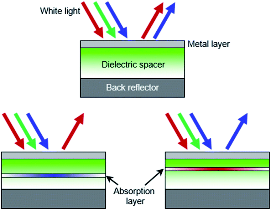 | ||
| Fig. 1 Light absorption/reflection in MIM cavities without and with an absorption layer. | ||
Fig. 2(a) shows an asymmetric F–P cavity structure consisting of a SiO2 dielectric spacer with thickness d sandwiched between a 100 nm-thick Al back reflector and a 10 nm-thick Au layer. The resonance condition is given as follows:28–30
 | (1) |
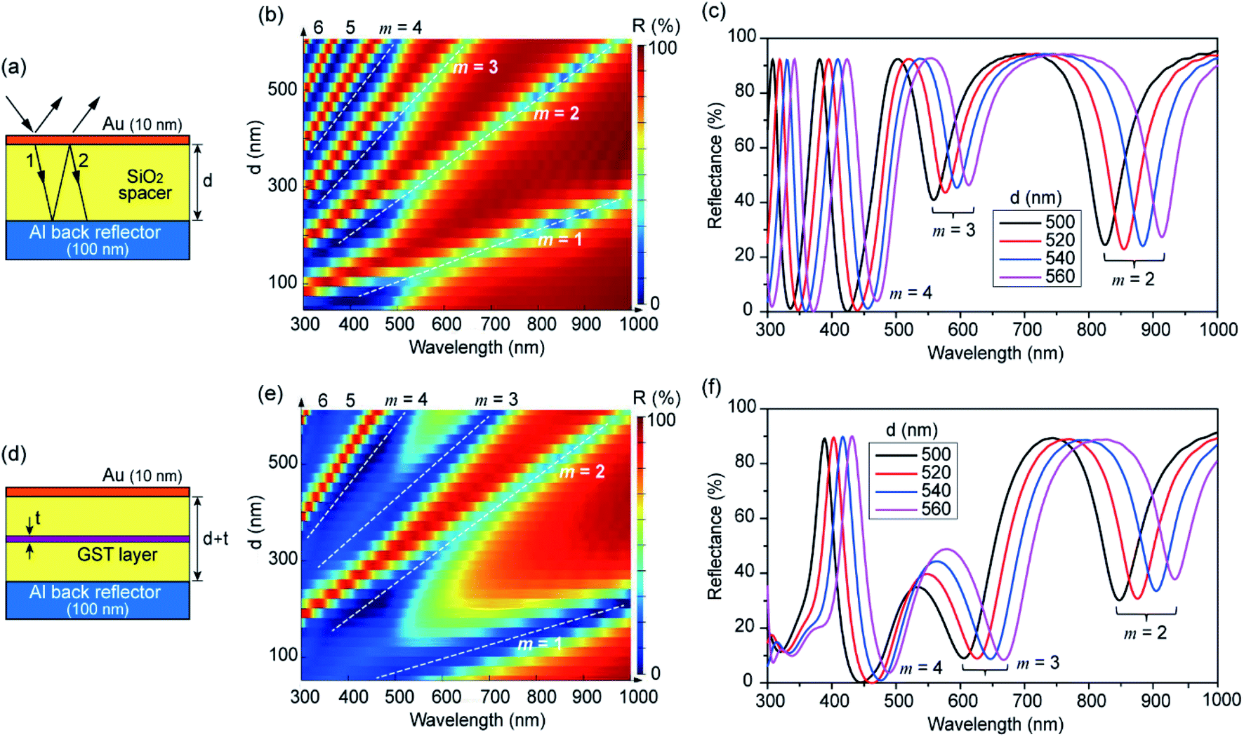 | ||
| Fig. 2 (a) MIM cavity structure used for FDTD simulation. (b) Normal-incidence reflectance (R) of the MIM structure calculated as functions of SiO2 thickness and light wavelength. (c) Reflectance spectra of the MIM structure observed at different d values of 500, 520, 540, and 560 nm. (d) MIGIM structure with a Ge2Sb2Te5 (GST) layer embedded at the center of the SiO2 spacer. (e) Reflectance of the MIGIM structure calculated as functions of SiO2 thickness and light wavelength (t = 7.2 nm). (f) Reflectance spectra of the MIGIM structure observed at different d values. | ||
Fig. 2(d) illustrates a cavity structure with a GST layer embedded at the center of the SiO2 spacer. It is well known that GST undergoes a phase transition between amorphous and crystalline states.32,33 The reason that we chose GST for this study is because it is also highly absorbing in the visible range. It has a complex refractive index, Ng = ng + ikg, and the real and imaginary parts of the index are both large. This makes the imaginary part (ε′′ = 2ngkg) of its dielectric constant large, thus resulting in high absorption. Fig. 3 shows the refractive indices (ng and kg) of two amorphous-state GST films deposited by sputtering for durations of 1 and 3 min. The refractive indices measured using ellipsometry were nearly independent of the thickness. The thickness of the film deposited for 3 min was measured to be 21.6 nm, and the film grown for 1 min was estimated to have one-third thickness, ∼7.2 nm. Because a film with a thickness of 21.6 nm resulted in excess absorption, the GST thickness (t) in the cavity design was fixed at 7.2 nm and the refractive indices measured at this thickness were used for the FDTD simulation. As a GST layer with thickness t is inserted into the cavity, the resonance condition is modified as (4π/λres)(nd + ngt) + ϕb + ϕt + ϕg = 2πm, where ϕg refers to the phase shifts occurring at the SiO2–GST interfaces. Although GST has a larger refractive index than SiO2, d is much larger than t. This can compensate for the difference in the refractive index, leading to a slight shift in the resonance wavelength. The structure shown in Fig. 2(d) is hereafter denoted as MIGIM, in comparison to the MIM structure of Fig. 2(a). Fig. 2(e) maps the reflectance of the MIGIM structure as functions of d and λ. Compared to Fig. 2(b), the resonance bands are slightly shifted. A more remarkable change resulting from the addition of a thin GST layer is that the high-reflectance bands between the resonance modes m = 1 and 2, m = 3 and 4, and m = 5 and 6 are significantly diminished. The reduced reflectance can be clearly observed in Fig. 2(f), which shows the spectra for values of d ranging from 500 to 560 nm. The reflection peaks between m = 3 and 4 (and m = 5 and 6) are significantly weakened, whereas the peaks between m = 2 and 3 (and m = 4 and 5) remain unchanged. Similar phenomena were observed when the top metal layer was replaced with an Ag film. The reflectance maps for the MIM and MIGIM structures with a 10 nm-thick Ag top layer are shown in Fig. S1 (ESI†). The use of Au as the top layer causes wider absorption bands at λ < 500 nm, compared to the case with an Ag top layer. This is attributed to the inter-band transition of Au occurring in this range.
 | ||
| Fig. 3 Real (ng) and imaginary (kg) refractive indices of amorphous GST films deposited by sputtering for 1 and 3 min on glass substrates. | ||
To better understand the effect of a thin GST absorption layer, the distributions of electric field (E-field) intensity and absorbed power within the cavity were calculated using FDTD. Fig. S2(a) (ESI†) shows the reflectance spectrum obtained for the MIM structure of Au (10 nm)–SiO2 (420 nm)–Al (100 nm). The resonance peak observed at λ = 490 nm corresponds to m = 3. Fig. S2(b) and (c) (ESI†) show the E-field intensity and absorbed power distributions across the structure at this resonance wavelength, respectively. Because the top Au layer is subject to a high E-field, the incident light is strongly absorbed by it. A small fraction of the optical power is also absorbed by the bottom Al reflector. We now consider two reflection peaks on both sides of this resonance, which are observed at 430 and 610 nm. The wavelengths of these two peaks are denoted as λ1 and λ2, respectively, in Fig. 4(a). Fig. 4(b) depicts the field intensity and absorbed power distributions at λ1. As the wavelength changes from 490 to 430 nm, the intensity distributions also change. Fig. 4(c) shows the distributions observed at λ2. At both λ1 and λ2, the E-field intensity around the top Au layer is extremely low although the two wavelengths exhibit different intensity distributions. This makes the incident light highly reflective with negligible absorption by the top metal layer. Fig. 4(d) shows the reflectance spectrum obtained when a GST layer is inserted at the center of the SiO2 spacer; thus, the MIGIM structure is Au (10 nm)–SiO2 (210 nm)–GST (7.2 nm)–SiO2 (210 nm)–Al (100 nm). As the optical path length increases, the resonance peak slightly redshifts. The two reflection peaks also shift to λ3 and λ4. As a more prominent effect, the peak at λ3 exhibits a significantly lower reflectance than the original peak at λ1, whereas the longer-wavelength peak at λ4 has nearly the same reflectance as the peak at λ2. Fig. 4(e) and (f) show the field intensity and absorbed power distributions at λ3 and λ4, respectively. In Fig. 4(b) and (c), the E-field intensity has alternate maxima and minima within the SiO2 spacer, depending on the position. The period of the intensity profile also varies with the wavelength of the incident light. The center (i.e., the middle position) of the SiO2 spacer is the intensity-maximum region at λ1, whereas it is the minimum region at λ2. Thus, even if a GST layer is inserted at the same position, the amount of optical power absorbed by this layer depends on the light wavelength, as shown in Fig. 4(e) and (f). Fig. 4(g) shows the reflectance spectrum obtained when the GST layer is moved upward from the center position to have an MIGIM structure of Au (10 nm)–SiO2 (140 nm)–GST (7.2 nm)–SiO2 (280 nm)–Al (100 nm). Now, the longer-wavelength reflection peak (λ6) shrinks, whereas the shorter-wavelength peak (λ5) remains unaffected. This is because the new GST position is an intensity-maximum region at λ6 but a minimum region at λ5. Clearly, the optical power absorbed by the GST layer is much larger at λ6 than at λ5, as shown in Fig. 4(h) and (i).
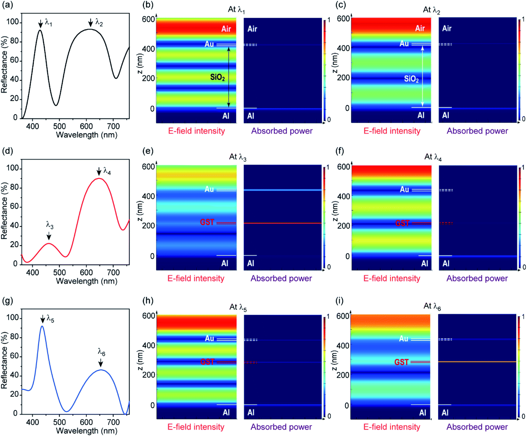 | ||
| Fig. 4 (a) Reflectance spectrum obtained for the MIM structure of Au (10 nm)–SiO2 (420 nm)–Al (100 nm). (b and c) E-field intensity and absorbed power distributions at λ1 and λ2, respectively. (d) Reflectance spectrum of the MIGIM structure of Au (10 nm)–SiO2 (210 nm)–GST (7.2 nm)–SiO2 (210 nm)–Al (100 nm). (e and f) E-field intensity and absorbed power distributions at λ3 and λ4, respectively. (g) Reflectance spectrum of the MIGIM structure of Au (10 nm)–SiO2 (140 nm)–GST (7.2 nm)–SiO2 (280 nm)–Al (100 nm). (h and i) E-field intensity and absorbed power distributions at λ5 and λ6, respectively. | ||
The positions of the reflection peaks change with the thickness of the dielectric spacer. Fig. 5(a) shows the reflectance spectra of the MIM structure with d ranging from 280 to 400 nm. Because there are two reflection peaks in the visible range, the colors produced are not pure, as shown in Fig. 5(e). Fig. 5(b) shows the spectra when a GST layer is inserted into the center of the SiO2 spacer. Regardless of the thickness of the spacer, d, the shorter-wavelength reflection peaks become significantly weakened. Fig. 4(b) shows the E-field intensity distribution in the MIM structure at λ1. The peak wavelength λ1 changes with a change in d. However, the E-field distribution for this shorter-wavelength reflection peak maintains the same shape because the change in the wavelength compensates for the change in the spacer thickness. That is, the center of the spacer is always an intensity-maximum region regardless of its thickness. Therefore, the short-wavelength reflection peaks can be suppressed by placing a GST layer at the center of the SiO2 spacer. This leads to an improved color purity (see “MIGIM (handbook)” in Fig. 5(e)). Although the color purity can be enhanced by embedding a thin GST absorption layer, it needs to be further improved because the MIGIM structure still exhibits a high reflectance at long visible wavelengths. The reflectance spectra and the corresponding colors for this structure (Fig. 5(b) and (e)) were calculated using the handbook refractive indices of Au. The optical characteristics of the asymmetric F–P cavity are also influenced by the optical constant of the top metal layer.21,27 Thin films may have refractive indices different from the bulk-state handbook data. In a previous report,19 we showed that the refractive indices of Au and Ag films deposited by thermal evaporation are strongly thickness dependent and coincide with the handbook data only for thicknesses over 40 nm. For a 10 nm-thick Au film, the real part of the refractive index was comparable to its imaginary part at wavelengths longer than 600 nm, being highly lossy in this spectral range. The refractive indices measured for Au films are shown in Fig. S3 (ESI†). The MIGIM structure based on the refractive index measured for a 10 nm-thick Au film is denoted as “MIGIM (measured)” to distinguish from the MIGIM (handbook) structure. Fig. 5(c) shows the reflectance of the MIGIM (measured) structure mapped as functions of d and λ. The high-reflectance band between m = 1 and 2 observed in the MIGIM (handbook) structure (Fig. 2(e)) is absent from the MIGIM (measured) structure, leaving a narrower reflection band in the visible range. Fig. 5(d) plots the reflectance spectra of the MIGIM (measured) structure for d values of 280–400 nm. A single reflection peak with a bandwidth of ∼100 nm and a reflection efficiency of 90.8% is achievable. Consequently, more vivid colors can be obtained, as shown in Fig. 5(e). The simulation colors shown in Fig. 5(e) are to compare the purity of colors obtainable from the three different structures, and they are not directly associated with the reflectance spectra shown in Fig. 5(a), (b), and (d).
 | ||
| Fig. 5 (a and b) Reflectance spectra of MIM and MIGIM (handbook) structures with a d of 280–400 nm, respectively. (c) Reflectance of the MIGIM (measured) structure mapped as functions of d and λ. (d) Reflectance spectra of the MIGIM (measured) structure. (e) Simulation colors from MIM, MIGIM (handbook), and MIGIM (measured) structures. | ||
We investigated the optimum refractive indices for the absorption layer (AL). Fig. 6 shows the reflectance spectra simulated for the cavity structure of Au (10 nm)–SiO2 (210 nm)–AL (7.2 nm)–SiO2 (210 nm)–Al (100 nm). In the absence of the AL, the cavity revealed two reflection peaks in the visible range. To completely suppress the shorter-wavelength peak, the real (n) and imaginary (k) indices of the AL should be both large. If only one of the indices is large (i.e., small n and large k or large n and small k), the corresponding material does not function well as the AL because it is highly reflective rather than absorptive. For instance, Fig. 6(a) shows how the reflectance spectra vary with k when n = 1. The optimum indices were found to be n = 3 and k = 3 (Fig. 6(b)). However, materials having such large n and k values simultaneously are rare. A material with n = 4 and k = 2 was also effective as the AL, as shown in Fig. 6(c). GST roughly satisfies this condition although its k value slowly decreases with increasing wavelength. In this cavity design study, the thickness of the GST layer was fixed at t = 7.2 nm. For t < 5 nm, absorption by the layer was not enough to significantly suppress the shorter-wavelength reflection peak, thereby deteriorating the color purity. A GST layer with t > 10 nm decreased the reflection efficiency to less than 90%. Fig. 5(d) plots the reflectance spectra of the MIGIM (measured) structure for t = 7.2 nm. For comparison, Fig. S4† (ESI†) shows the reflectance spectra calculated for t = 3.6 nm and 14 nm.
 | ||
| Fig. 6 Effects of the refractive indices n and k of the absorption layer (AL) on reflectance spectra: (a) n = 1, (b) n = 3, and (c) n = 4. Cavity structure is Au (10 nm)–SiO2 (210 nm)–AL (7.2 nm)–SiO2 (210 nm)–Al (100 nm). | ||
To experimentally verify the simulation results, the MIGIM (measured) structures were fabricated on Si substrates. Various colors including high-purity R/G/B can be generated from the structures, as shown in Fig. 7(a). Fig. 7(b) compares the simulation and experimental spectra for the primary R/G/B colors. Fig. 7(c) shows the transmission electron microscopy images of a MIGIM (measured) sample. The Au and GST layers were not flat, which might have resulted from the rough surface of an Al back reflector. In addition, the thickness of the GST layer was a little higher than the target thickness of 7.2 nm. The slight discrepancy between the simulation and experimental spectra is attributable to these factors. Like the top Au layer, the Al back reflector was also deposited by thermal evaporation. A sputter-deposited Al back reflector may reveal a more flattened surface, leading to better consistency between the simulation and experimental results. Fig. S5† (ESI†) shows the dependence of the reflectance spectra and colors on the incident angle of light investigated with a red-color sample. The red color was quite robust up to an incident angle of 15°. As the angle increased to 30°, 45°, and 60°, the color gradually changed to scarlet, orange, and yellow. SiO2 is a low-index material (n ≈ 1.5). The use of a dielectric spacer with a higher index may improve the angle tolerance of the color because a higher-index material maintains its refraction angle small over a wider angle range. Fig. 7(d) shows the simulation and experimental colors mapped on the CIE 1931 diagram, indicating that a wide variety of colors can be generated simply by varying the thickness of the SiO2 spacer. These colors were experimentally demonstrated. Fig. 7(e) shows a Si wafer displaying diverse colors. The MIGIM structure has two SiO2 layers, i.e., one below the GST layer and the other above it. When the SiO2 layers were deposited by sputtering, the Si wafer was tilted such that the layers had position-dependent, gradient thicknesses.
 | ||
| Fig. 7 (a) Colors from MIGIM (measured) samples. “d” is the thickness of the SiO2 layer. (b) Comparison between the simulation and experimental spectra. (c) Transmission electron microscopy images of a MIGIM (measured) sample. (d) Simulation and experimental colors mapped on the CIE 1931 diagram. Polygons in red color represent the experimental colors. (e) Si wafer displaying diverse colors, where the SiO2 layers have position-dependent, gradient thicknesses. | ||
Conclusion
We showed that reflective colors with high purity and brightness can be obtained by embedding an ultrathin GST absorption layer in a MIM cavity comprising continuous Au–SiO2–Al layers. The MIM cavity acts as a band-stop filter in reflection mode to reveal subtractive C/M/Y colors because it resonantly absorbs a narrow wavelength range and reflects the rest of the spectrum. Our approach to generating additive R/G/B colors is to create another absorption band in addition to the F–P resonance by placing a thin absorption layer in a high-intensity region within the SiO2 spacer. Using a thermally evaporated 10 nm-thick Au film as the top metal layer, this approach led to highly pure and bright R/G/B colors with a bandwidth of ∼100 nm and reflectivity of 90%. The color was tunable simply by varying the thickness of the dielectric spacer. The results of this study may be effectively utilized in a wide variety of areas, including reflective displays, solar cells, colorimetric sensors, and surface decoration.Conflicts of interest
There are no conflicts of interest to declare.Acknowledgements
This work was supported by the National Research Foundation of Korea (NRF) grant funded by the Korea government (MSIT) (NRF-2020R1A2C2003575) and the R&D convergence program of the National Research Council of Science & Technology of Korea (No. CAP-16-10-KIMS).References
- K. Lee, S. Han, Z. Li, H. Baac and H. Park, Sci. Rep., 2019, 9, 14917 Search PubMed.
- Y. Gu, L. Zhang, J. Yang, S. Yeo and C. Qui, Nanoscale, 2015, 7, 6409 Search PubMed.
- B. Zeng, Y. Gao and F. Bartoli, Sci. Rep., 2013, 3, 2840 Search PubMed.
- S. Wu, B. Huang, Y. Wu, Z. Meng and S. Zhang, Nanoscale, 2020, 12, 11460 Search PubMed.
- S. Kang, Y. Zhao, W. Wang, T. Zhang, T. Chen, H. Yi, F. Rao and S. Song, Optica, 2015, 2, 589 Search PubMed.
- D. Chen, T. Wang, G. Song, Y. Du, J. Lv, X. Zhang, Y. Li, L. Zhang, J. Hu, Y. Fu and R. Jordan, ACS Appl. Mater. Interfaces, 2019, 11, 41668 Search PubMed.
- Z. Wang, X. Wang, S. Cong, J. Chen, H. Sun, Z. Chen, G. Song, F. Geng, Q. Chen and Z. Zhao, Nat. Commun., 2020, 11, 302 Search PubMed.
- K. Lee, J. Lee, S. Seo and L. Guo, Light Sci. Appl., 2014, 3, e215 Search PubMed.
- L. Wen, Q. Chen, F. Sun, S. Song, L. Jin, Y. Yu and A. Ruiz-Canales, Sci. Rep., 2014, 4, 7036 Search PubMed.
- D. Kim, S. Choi, H. Cho and J. Sun, Adv. Mater., 2019, 31, 1804080 Search PubMed.
- S. Banisadr, A. Oyefusi and J. Chen, ACS Appl. Mater. Interfaces, 2019, 11, 7415 Search PubMed.
- J. Ko, Y. Yoo, Y. Kim, S. Lee and Y. Song, Adv. Funct, Mater., 2020, 30, 1908592 Search PubMed.
- S. Rezaei, J. Ho, A. Naderi, M. Yaraki, T. Wang, Z. Dong, S. Ramakrishna and J. Yang, Adv. Optical Mater., 2019, 7, 1900735 Search PubMed.
- X. Su, H. Xia, S. Zhang, B. Tang and S. Wu, Nanoscale, 2017, 9, 3002 Search PubMed.
- H. Wu, Y. Jiao, C. Zhang, C. Chen, L. Yang, J. Li, J. Ni, Y. Zhang, C. Li, Y. Zhang, S. Jiang, S. Zhu, Y. Hu, D. Wu and J. Chu, Nanoscale, 2019, 11, 4803 Search PubMed.
- L. Feng, P. Huo, Y. Liang and T. Xu, Adv. Mater., 2019, 1903787 Search PubMed.
- A. Kristensen, J. Yang, S. Bozhevolnyi, S. Link, P. Nordlander, N. Hallas and N. Mortensen, Nat. Rev. Mater., 2017, 2, 16088 Search PubMed.
- B. Yang, W. Liu, Z. Li, H. Cheng, D. Choi, S. Chen and J. Tian, Nano Lett., 2019, 19, 4221 Search PubMed.
- J. Kim, H. Oh, M. Seo and M. Lee, ACS Photonics, 2019, 6, 2342 Search PubMed.
- Z. Yang, C. Ji, D. Liu and L. Guo, Adv. Optical Mater., 2019, 7, 1900739 Search PubMed.
- S. Kim, H. Choi, H. Lee and S. Hong, ACS Appl. Mater. Interfaces, 2019, 11, 7280 Search PubMed.
- A. Ghobadi, H. Hajian, M. Soydan, B. Butun and E. Ozbay, Sci. Rep., 2019, 9, 290 Search PubMed.
- G. Kenanakis, Ch. P. Mavidis, E. Vasilaki, N. Katsarakis, M. Kafesaki, E. N. Economou and C. M. Soukoulis, Appl. Phys. A, 2017, 123, 77 Search PubMed.
- Z. Yang, Y. Zhou, Y. Chen, Y. Wang, P. Dai, Z. Zhang and H. Duan, Adv. Opt. Mater., 2016, 4, 1196 Search PubMed.
- C. Park, V. Shrestha, S. Lee and D. Choi, Sci. Rep., 2016, 6, 25496 Search PubMed.
- Z. Li, S. Butun and K. Aydin, ACS Photonics, 2015, 2, 187 Search PubMed.
- Z. Liu, X. Liu, S. Huang, P. Pan, J. Chen, G. Liu and G. Gu, ACS Appl. Mater. Interfaces, 2015, 7, 4962 Search PubMed.
- B. Lee and M. Zhang, J. Appl. Phys., 2006, 100, 063529 Search PubMed.
- K. Bhattarai, S. Silva, K. Song, A. Urbas, S. Lee, Z. Ku and J. Zhou, Sci. Rep., 2017, 7, 10569 Search PubMed.
- M. Aalizadeh, A. Khavasi, B. Butun and E. Ozbay, Sci. Rep., 2018, 8, 9162 Search PubMed.
- D. R. Ride, CRC Handbook of Chemistry and Physics, CRC Press, 88th edn, 2007 Search PubMed.
- Q. Yin and L. Chen, J. Alloys Compd., 2019, 770, 692 Search PubMed.
- U. Ross, A. Lotnyk, E. Thelander and B. Rauschenbach, J. Alloys Compd., 2016, 676, 582 Search PubMed.
Footnote |
| † Electronic supplementary information (ESI) available. See DOI: 10.1039/d0na00626b |
| This journal is © The Royal Society of Chemistry 2020 |