DOI:
10.1039/D0NA00602E
(Communication)
Nanoscale Adv., 2020,
2, 4410-4416
Enhanced flux of chemically induced hot electrons on a Pt nanowire/Si nanodiode during decomposition of hydrogen peroxide†
Received
13th June 2020
, Accepted 23rd July 2020
First published on 7th August 2020
Abstract
Identifying the charge transfer at metal–semiconductor interfaces by detecting hot electrons is crucial for understanding the mechanism of catalytic reactions and the development of an engineered catalyst structure. Over the last two decades, the development of catalytic nanodiodes has enabled us to directly measure chemically induced hot electron flux and relate it to catalytic activity. A crucial question is the role of interfacial sites at metal–oxide interfaces in determining catalytic activity and hot electron flux. To address this issue, a new design of catalytic nanodiodes employs nanoscale Pt wires and a semiconducting substrate. Here, we fabricated a novel Schottky nanodiode, a platinum nanowire (Pt NW) deposited Si catalytic nanodiode (Pt NW/Si) that exhibits an increased number of metal–semiconductor interfacial sites (Pt/Si) compared with a Pt film-based Si nanodiode (Pt film/Si). Two types of Pt/Si catalytic nanodiodes were utilized to investigate the electronic properties of the Pt/Si interface by detecting hot electrons and observing reactivity during the H2O2 decomposition reaction in the liquid–solid system. We show that the Pt NWs had higher catalytic activity because of the surface defect sites on the Pt NW surface. We observed a higher chemicurrent yield on the Pt NW/Si nanodiode compared with the Pt film/Si nanodiode, which is associated with the shortened travel length for the hot electrons at the edge of the Pt nanowires and results in a higher transmission probability for hot electron transport through metal–oxide interfaces.
1 Introduction
Understanding the mechanism of catalytic reactions in heterogeneous catalysis is crucial in identifying the reactivity, selectivity, and stability of a catalyst.1,2 Numerous studies have demonstrated the importance of charge transport at the metal–oxide interface, which acts as a catalytically active site.3,4 The electronic properties of a catalyst can be manipulated by controlling the size and shape of the catalyst or by changing the support.5 However, it has been challenging to identify the electronic structure of the metal–support interfaces of nanocatalysts during chemical reactions.
Recently, a metal–semiconductor catalytic Schottky nanodiode has been a powerful tool for investigating the mechanisms of catalytic reactions on metal surfaces.6,7 When an exothermic reaction takes place and external energy is transferred onto a metal catalyst, several elementary processes are carried out to dissipate heat. Through non-adiabatic dissipation, most of the energy is converted into energetic hot electrons that have a short lifetime of a few femtoseconds and a high energy of 1–3 eV. Hot electrons can be extracted by overcoming the Schottky barrier formed at the metal–semiconductor interface and give insight into charge transfer during surface reactions.8–10 Thus, studies of the correlation between the hot electron flow and catalytic reactivity by detecting hot electrons generated during chemical reactions on metal–oxide Schottky nanodiodes have been conducted. The quantification of the hot electron flow demonstrates a notoriously strong relationship between the activation energy obtained from turnover rates and chemicurrents.11,12 Furthermore, scientists have studied charge transfer between metal nanoparticles and supports by measuring hot electron flux during catalytic reactions and observing the increase in hot electrons as the number of metal–oxide interfacial sites increases.13–15
To date, research into detecting hot electrons has been mainly implemented in gas–solid environments.6,16–18 However, various reactions (e.g., in eco-friendly and sustainable H2-based energy systems or CO2 reduction reactions) are carried out in the liquid phase on solid-state catalysts; hydrogen peroxide (H2O2) is formed as an intermediate reaction product during these reactions. Therefore, it is necessary to understand the factors that accelerate the reaction rate of hydrogen peroxide decomposition. Direct observation of the mechanism of the H2O2 decomposition reaction has proven that electric charge transfer occurs between the catalyst and ions by experimentally measuring the hot electron flux in a liquid–solid system.19–22 Theoretically, the 2.04 eV released from the H2O2 decomposition reaction is sufficient for hot electrons to overcome the Schottky barrier formed between the Pt and the silicon (Fig. 1a).
 |
| | Fig. 1 (a) Principle of probing hot electrons on a Pt/Si nanodiode during decomposition of hydrogen peroxide. (1) Excitation and (2) ballistic transport of a hot electron through the metal–semiconductor Schottky contact; φb is the Schottky barrier height, Ec is the conduction band minimum, Ev is the valence band maximum, and EF is the Fermi level. Catalytic nanodiodes consisting of (b) a Pt film and (c) Pt nanowires deposited on Si. | |
Here, we report the dynamic behavior of hot electrons and charge transport through the metal–semiconductor interface by controlling the geometric structure of the catalyst. To examine the effect of charge transfer at the metal–semiconductor interface, two types of catalytic nanodiodes with different sizes and shapes of Pt catalysts were prepared- the nanodiodes consisted of a Pt film-based Si substrate (Pt film/Si) and highly ordered platinum nanowires transfer-printed on a Si substrate (Pt NW/Si) (Fig. 1b, c). Chemicurrent and O2 evolution rates were measured during the H2O2 decomposition reaction in a liquid–solid environment. The catalytic activity and hot electron generation were enhanced in Pt NW/Si, and we conclude that the increase in hot carrier transfer at the Pt NW/Si interface is associated with the shorter travel length required for the hot electrons at the Pt/Si interface.
2 Experimental
2.1 Fabrication of the Pt/Si catalytic nanodiode
To fabricate the Pt film/Si nanodiode, a 10 nm Pt film and Au/Ti ohmic contact were deposited on an n-type Si substrate using e-beam deposition to form a metal–semiconductor Schottky contact. First, 6-inch n-type silicon (100) wafers were cleaned with HF to remove any oxide layers; the etched Si wafers were then stored immediately in an envelope filled with argon gas. For the e-beam deposition, the Si substrate was covered with a stainless-steel mask, taken into an electron beam chamber, and then 10 nm of Pt was deposited onto the exposed Si surface. Next, the ohmic contact was deposited beside the Pt layer using 50 nm of Ti and 50 nm of Au. The area of the Pt–Si Schottky contact was 116 mm2, and the ohmic contact area was 28 mm2.
For Pt NW/Si, the same Au/Ti ohmic contact was deposited on an oxide-free Si substrate, and the as-prepared nanowires were imprinted on the Si wafer. The Pt nanowires were fabricated using the solvent-assisted nano-transfer printing (S-nTP) method, as shown in Fig. S1 in the ESI.†
2.2 Measurement of the hot electrons and catalytic activity on the Pt/Si nanodiode in the liquid–solid reactor
Fig. S2 in the ESI† shows the liquid–solid catalytic reactor for measuring chemicurrent and the O2 evolution rates during the H2O2 decomposition reaction on the Pt/Si nanodiode surface. The reactor basically consists of four parts: a sample cell, a manipulator, a chemicurrent measurement apparatus, and a pressure gauge. A 5 wt% aqueous solution of H2O2 was prepared using 35 wt% H2O2 (Junsei Chemical Co., Ltd.) and DI water. The temperature in the laboratory was maintained at 24 °C, and light was prevented from entering the reactor. At first, the Pt/Si nanodiode was connected to the manipulator in the reactor and a freshly prepared 5 wt% H2O2 solution was poured into the sample cell. A closed system was created by connecting the sample cell to the reactor without any leakage. Once the Pt/Si catalytic nanodiode was immersed in the H2O2 solution, hot electrons were generated on the Pt surface, and excited hot electrons crossed the Pt/Si Schottky barrier and were detected as a chemicurrent with time by using a Keithley 2400. The pressure change inside the reactor caused by the evolution of O2 gas was measured using a 120AA Baratron pressure manometer. The composition of the evolved gas during the H2O2 decomposition reaction was analyzed by using a HPR-20 QIC quadrupole mass spectrometer system, Hiden Analytical Limited.
2.3 Characterization
The current–voltage (I–V) curve and short-circuit current were measured using a Keithley 2400 source meter. Scanning electron microscopy (SEM) was performed using a HITACHI SU8230. Transmission electron microscopy (TEM) was conducted using a Tecnai G2 F30 S-Twin at 300 kV. The X-ray photoelectron spectroscopy (XPS) spectra were measured using a Thermo VG Scientific with an Al-Kα source under ultra-high vacuum conditions. The X-ray diffraction (XRD) was carried out using a D/MAX-2500 RIGAKU with a Cu Kα source.
3 Results and discussion
3.1 Characterization of Pt/Si catalytic nanodiodes
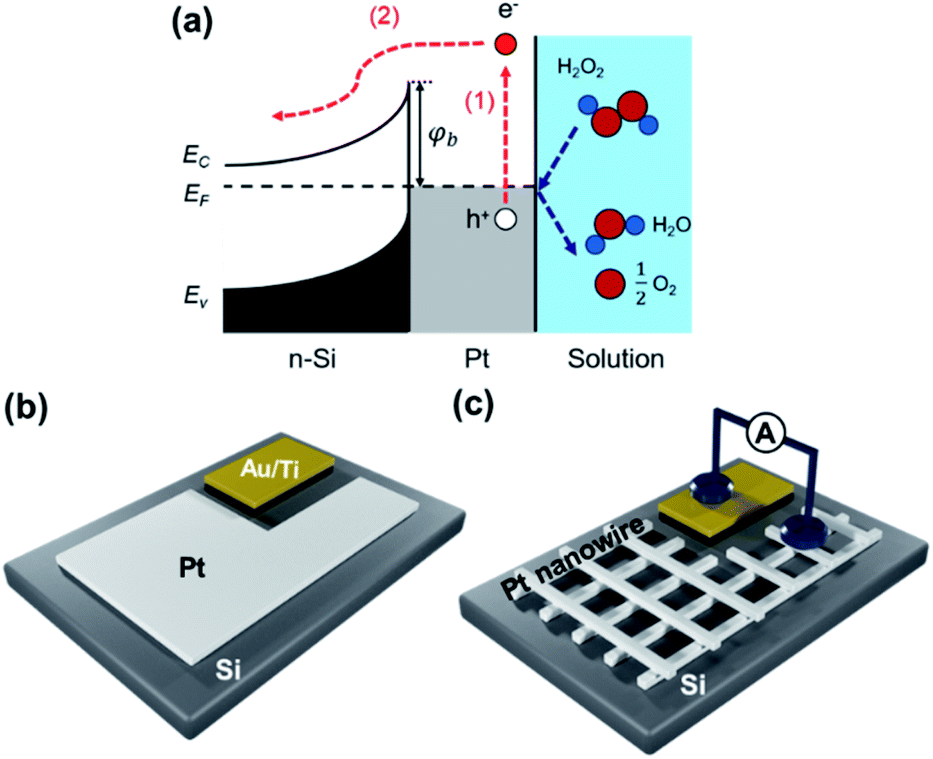
The structural and chemical characteristics of the Pt/Si nanodiodes were analyzed using SEM, TEM, XPS, and XRD analysis. As shown in the TEM and SEM images (Fig. 2a, b), the Pt NWs fabricated using the S-nTP method have a period of 50 nm, a width of 25 nm, and a height of around 12 nm, while the deposited Pt film has a thickness of 10 nm. The area in which the catalytic nanodiode is immersed in the H2O2 solution is equal to 0.8 cm2 for both the Pt film and Pt NWs. However, the interfacial area of the Pt NW/Si interface and the active catalytic surface area of the Pt NWs differ from those for the Pt film, because the grid-patterned Pt NWs form a distinct shape and arrangement compared with the Pt film. Based on the microscopy images, it can be seen that Pt NWs have a calculated contact area of 0.35 cm2 and catalytic surface area of 1.6 cm2. To identify the surface oxidation state of the Pt film and Pt NWs, we examined the Pt 4f XPS spectra before and after the reaction (Fig. S3 in the ESI†). Upon deconvolution of the XPS spectra, the Pt 4f7/2 and 4f5/2 peaks appeared at ∼71.5 and ∼74.8 eV, respectively, for both the Pt film and Pt NWs. Fitting the XPS spectra showed that the surface of the Pt thin film is mainly composed of metallic Pt (Pt0), whereas the Pt NWs contain 16.9% PtO (Pt2+) and 9.5% PtO2 (Pt4+). Fig. S4 in the ESI† shows the XRD analysis; the diffraction peaks at about 2θ = 39.8, 46.0, 67.6, and 81.2 correspond to the (111), (200), (220), and (311) planes of the face-centered cubic (fcc) structure of Pt. The Pt (111) peak was predominantly observed for the Pt film, whereas the Pt (111), (200), (220), and (311) peaks appeared for the Pt NWs. Furthermore, the HRTEM image of Pt NWs shows various crystalline structures of Pt (111), (200), (220) and (311) unlike the Pt film for which the (111) plane is dominant (Fig. S5 a, b†). This is because non-preferential crystal orientation formation was achieved due to the high surface energy of the PMMA replica and angle deposition of Pt NWs manufactured through the S-nTP method.23 The results of the HRTEM and SAED patterns of Pt NWs are in line with the result of XRD, which clearly indicates the difference in the crystal structure between the Pt NWs and Pt film.
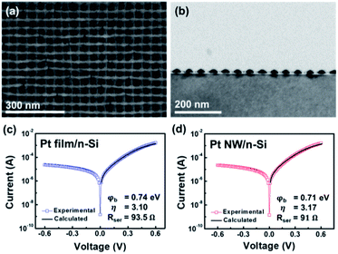 |
| | Fig. 2 (a) SEM image of two layers of Pt NWs stacked on a Si substrate. (b) TEM cross sectional image of the Pt NWs. Current–voltage curves of the (c) Pt film/Si and (d) Pt NW/Si nanodiodes. | |
3.2 Current–voltage (I–V) measurements
The presence of the Schottky barrier at the Pt/Si interface enables the collection of hot electrons, which were thermalized several femtoseconds after being created on the metal surface. When the energy of the hot electrons generated from the catalytic reaction is sufficient to overcome the Schottky barrier height, hot electrons are detected as a current in the nanodiode. Therefore, it is important to measure the Schottky barrier height and the electrical properties of the Pt/Si nanodiode using the current–voltage (I–V) curve. Furthermore, platinum silicide (PtSi) is known to form at some Pt–Si interfaces at temperatures as low as 200 °C, and PtSi can affect the Pt/Si barrier height. As we measure the I–V curve of the Pt/Si nanodiode, we can evaluate the properties of Pt–Si junctions.24,25 According to the thermionic emission theory (eqn (1)), the Schottky barrier is obtained as follows:26| | 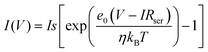 | (1) |
where 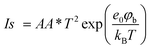 is the saturation current, A is the area of the Schottky contact, A* is the Richardson constant, T is the temperature, e0 is the elementary charge, φb is the Schottky barrier height, kb is the Boltzmann constant, V is the voltage, Rser is the series resistance, and η is the ideality factor. In the forward-biased regime, the Schottky barrier can be easily calculated by fitting the reverse function V(I) to the experimentally measured I–V curves (eqn (2)).
| | 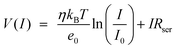 | (2) |
As a result of fitting the calculated I–V curves to the experimental I–V curves using the thermionic emission equation, the Schottky barriers (φb) formed in Pt film/Si and Pt NW/Si were 0.74 and 0.71 eV, respectively (Fig. 2c, d). The ideality factor (η) and series resistance (Rser) were 3.10 and 93.5 Ω for Pt film/Si, and 3.17 and 91 Ω for Pt NW/Si, respectively. Since the conductivity, ideality factor, and series resistance of the Pt film/Si and Pt NW/Si nanodiodes are similar, we can estimate an intimate contact and homogeneity at the Pt/Si interface for both nanodiodes.8,27–29 As the Schottky barrier height is affected by light, I–V curves were measured under rigorously dark conditions. As shown in Fig. S6,† when light was present, the Schottky barrier height of Pt film/Si was 0.69 eV, which was 0.05 eV smaller than the Schottky barrier height measured in the dark state.
3.3 Enhancement of chemicurrent
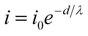
To investigate the flow of hot electrons generated on the Pt surface during H2O2 decomposition, we measured the chemicurrent, which refers to the evolution rate of hot electrons in the Pt film/Si and Pt NW/Si nanodiodes. In this study, hot electrons are created by the adsorption and decomposition of H2O2 molecules on the Pt surface and the subsequent formation of OH− species. In a typical liquid–solid system, we have a unique response of the current signal from the catalytic nanodiode caused by the generation of hot electrons at the liquid–solid interface (Pt catalyst/H2O2 aqueous solution). Fig. 3a shows the chemicurrent with respect to time; the peak chemicurrent is shown at the moment when the diode is immersed in the H2O2 solution (t = 3 s), and the current decreased gradually until reaching the steady-state chemicurrent. Formation of the peak and steady-state chemicurrents contributes to the mechanism of the H2O2 decomposition reaction. Initially, the H2O2 molecules approach the Pt surface and become ionized. The charged H2O2 molecules then decompose into OH and OH− near the Pt surface. The resulting OH and OH− species form H2O and O2 by participation in various chain reactions. Once the chain-breaking reaction occurs, OH becomes OH−, and this resulting OH− reacts with the H+ ions adsorbed on the Pt surface to form H2O. This mechanism is energetically favorable and has an accompanying free energy of −47 kcal mol−1 (i.e., 2.04 eV). Because 2.04 eV is greater than the Pt/Si Schottky barrier height (0.71–0.74 eV), hot electrons generated during the H2O2 decomposition reaction can overcome the Schottky barrier and are measured as a chemicurrent in the Pt/Si nanodiode.22,30 When the Pt/Si catalytic diode is first immersed in the H2O2 solution, the adsorption rate of the OH− ions is at its maximum because the Pt surface is clean; therefore the peak chemicurrent appears. After the OH− species are rapidly consumed, the current value decreases rapidly, and the steady-state current is then determined by the rate at which OH is adsorbed and consumed. The peak chemicurrent values for the Pt film/Si and Pt NW/Si nanodiodes are 0.178 and 0.203 μA, respectively; the steady-state chemicurrent values for the Pt film/Si and Pt NW/Si nanodiodes are 0.007 and 0.008 μA, respectively. However, since hot electrons can be detected only at the Schottky contact between the Pt and the Si, the chemicurrent should be normalized by dividing by the contact area between the Pt and the Si. Fig. 3b shows the normalized peak chemicurrent values, and Fig. 3c shows the normalized steady-state chemicurrent values for the Pt/Si nanodiodes. The normalized peak chemicurrents for the Pt film/Si and Pt NW/Si nanodiodes are 0.22 and 0.58 μA cm−2, respectively. The Pt NW/Si nanodiode has a normalized chemicurrent about 2.63 times higher than that for the Pt film/Si nanodiode. The normalized steady-state current for the Pt film/Si and Pt NW/Si nanodiodes is 0.009 and 0.023 μA cm−2, respectively. The normalized steady-state chemicurrent for Pt NW/Si is 2.6 times higher than that for the Pt film/Si nanodiode. Both the normalized peak chemicurrent and the normalized steady-state chemicurrent for Pt NW/Si increased 2.6 times compared with those for Pt film/Si. This is because both the peak and steady-state chemicurrent are determined by the same mechanism that can be explained by the rate at which OH ions adsorb and desorb on the Pt surface. The chemicurrent was measured under rigorously dark conditions to exclude the effect of the photocurrent generated by the light. As shown in Fig. S7,† when the light of 9 μA cm−2 illuminated the diode with a halogen lamp, the total value of the chemicurrent was changed to 3.2 μA by photocurrent. In addition, the Pt nanowires deposited as the second layer do not contact the Si substrate; the hot electrons moving through the metal film lose energy and decrease exponentially as the thickness of the metal film increases (eqn (3)):| |  | (3) |
where i represents the chemicurrent, i0 indicates the initial hot electron flow, d is the thickness of the metal film, and λ is the inelastic mean free path of the electrons in the metal film. Based on eqn (3), it was found that hot electrons generated on the second layer of the Pt NWs are difficult to detect in the Pt NW/Si nanodiode, because the travel lengths for the hot electrons are higher than 10 nm. Instead, hot electron detection can be enhanced near the edge of the Pt/Si interface, which is the triple phase boundary of the H2O2 solution, Pt catalyst, and Si substrate, where the travel distance of the hot electrons is shortened and the hot electron detection probability is significantly higher. Therefore, the flow of hot electrons intensified in Pt NW/Si where the perimeter of the metal–semiconductor (Pt/Si) interface is remarkably larger than that for the film. To further confirm the hot electron transfer enhancement due to the Pt/Si interface effect, we additionally fabricated a different type of Pt NW/Si (denoted as Pt NW*/Si) with a narrower period and width and correspondingly increased interface area and the higher contact area than Pt NW/Si. We then measured the chemicurrent of Pt NW*/Si with the same experimental conditions. Fig. S8 in the ESI† shows SEM and TEM cross sectional images of the Pt NWs* imprinted on Si. Also, as a result of Fig. S9,† which shows the enhanced chemicurrent and normalized chemicurrent value of Pt NW*/Si, we concluded that hot electron transfer was improved as the edge of the Pt/Si interface was increased.
 |
| | Fig. 3 (a) Chemicurrent signals for the Pt film/Si and Pt NW/Si nanodiodes during decomposition of 5 wt% H2O2. The chemicurrent and the normalized chemicurrent of Pt film/Si and Pt NW/Si obtained from (b) the peak chemicurrent and (c) the steady-state chemicurrent. | |
3.4 Enhancement of catalytic activity
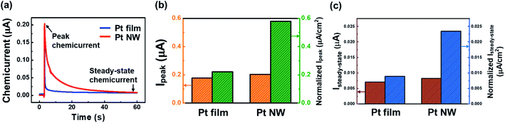
As described earlier, H2O2 is decomposed into O2 gas and H2O molecules on the surface of the Pt catalyst. As shown in Fig. S10 in the ESI,† oxygen gas evolved on both the Pt film and Pt NWs through the H2O2 decomposition reaction was detected by using a mass spectrometer. We obtained the rate of the H2O2 decomposition reaction on the Pt film and the Pt NW nanodiodes by measuring the pressure change inside the reactor caused by the production of O2 gas over time. While H2O2 molecules decompose on the Pt surface, the O2 gas evolves violently and escapes from the H2O2 solution. Fig. 4a shows a graph of pressure versus time; the slope of the graph indicates the O2 evolution rate. As shown in Fig. 4b, the O2 evolution rates for the Pt film/Si and Pt NW/Si nanodiodes were 0.716 and 2.03 μmol L−1 s−1, respectively. The higher O2 evolution rate of Pt NW/Si nanodiodes compared to Pt film/Si is visualized in the movie files (Movie S1 Pt NW.avi and Movie S2 Pt film.avi) in the ESI.† Since the O2 gas evolves on the whole surface exposed to the H2O2 solution, the normalized O2 evolution rate can be obtained by dividing the O2 evolution rate by the Pt surface area. The normalized O2 evolution rates for Pt film/Si and Pt NW/Si were 0.90 and 1.27 μmol L−1 s cm2, respectively. Several studies have been carried out that controlled the size and shape of the catalyst to identify the nature of the active metal sites and the reaction mechanism of catalytic reactions.31,32 On rough surfaces, atoms and molecules were found to bind more strongly at the atomic scale and these chemical bonds dissociate more easily. Rough surfaces that exhibit a high concentration of step edges and kink sites are catalytically active sites for carrying out structure-sensitive catalytic reactions.33–36 Studies of the effect of the Pt catalyst size on the electrocatalytic oxidation of methanol have reported that smaller Pt NPs with a larger fraction of corners and edge sites strongly bind oxygenated species.37 As shown in Fig. 2b, each Pt NW, unlike the Pt film, has a curved surface and naturally has more edges, and kinked and stepped sites on exposed surfaces than films. Therefore, we can conclude that the oxygen evolution rate was enhanced on the Pt NWs, which have a rough surface and a high concentration of stepped and kinked sites on the surface. This allows us to conclude that Pt NWs are more catalytically active than the Pt film, which is attributed to the difference in the catalyst structure.
 |
| | Fig. 4 (a) Pressure change over time during oxygen evolution on the surface of the Pt/Si nanodiodes in the reactor. (b) O2 evolution rate measured from each sample while normalizing with respect to the surface area. (c) The chemicurrent yield measured from the Pt film/Si and Pt NW/Si nanodiodes. (d) The scheme shows that the catalytic reaction and hot electron generation are promoted at the edge of the Pt nanowires. | |
3.5 Effect of the surface oxidation state of Pt on the chemicurrent yield
The surface oxidation state of catalysts affects the catalytic activity.38 As shown in Fig. S3 a–d in the ESI,† the surface of the Pt film is almost metallic, whereas the Pt NWs have a relatively high ratio of PtO and PtO2. Because the Pt oxide on the Pt NWs can affect the O2 evolution rate, we performed plasma treatment of the Pt film to oxidize the Pt film surface. First, we applied Ar plasma for 50 s, and then O2 plasma was applied for 10 s. An additional O2 plasma treatment was applied on the Pt film surface for 10 s. The surface of the Pt film after plasma treatment was characterized using XPS, and the ratios of PtO and PtO2 on the Pt film increased sharply to 54.8% and 17.6%, respectively (Fig. S3e,f in the ESI†). To investigate the effect of the Pt oxide produced on the surface of the Pt film by the plasma treatment, the H2O2 decomposition reaction was performed on the plasma-treated Pt film (Fig. S11†). In contrast to that in the bare Pt film, oxygen did not evolve over time on the Pt film following the plasma treatment, as visualized in Movie S3,† Pt film with plasma treatment.avi, in the ESI.† Therefore, it can be concluded that the presence of PtO and PtO2 on the Pt NW surface did not contribute to an increase in the reactivity of the Pt NWs; instead, the kinked, stepped and edge sites on the Pt NW surface enhanced the reactivity. The surface oxide also decreased the hot electron flux, because it acted as an insulator; however, the chemicurrent increased in Pt NW/Si because of the larger Pt/Si interface.
3.6 Origin of hot electron flow enhancement in Pt NW/Si
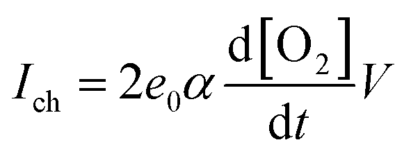
Theoretically, the quantity of hot electrons generated on the metal film surface is proportional to the catalytic reactivity.11,39 However, we utilized two different structures of the metal catalyst (i.e., Pt film and Pt nanowires) to distinguish the charge transport mechanism at the metal–semiconductor interface. To gain more insight into the origin of the hot electron flux in Pt/Si nanodiodes, we calculated the chemicurrent yield. The chemicurrent yield (α) is the number of hot electrons detected per oxygen molecule produced; it can be obtained using eqn (4):| | 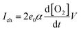 | (4) |
where Ich is the normalized peak chemicurrent, e0 is the elementary charge, α is the chemicurrent yield, d[O2]/dt is the normalized O2 evolution rate, and V is the volume of the liquid–solid reactor. Based on eqn (4), it can be seen that the chemicurrent yield (Fig. 4c) of Pt NW/Si was higher (about α = 2.37 × 10⁻⁵ electrons/O2 molecule) than that of Pt film/Si (α = 1.29 × 10⁻⁵ electrons/O2 molecule). These results reveal that the hot electrons formed in Pt NW/Si from excessive energy produced during the H2O2 decomposition reaction also overcome the Schottky barrier compared with those in Pt film/Si. Since hot electrons generated from the second layer of Pt NWs do not contribute to the chemicurrent signal, the first layer of Pt NWs, which is in direct contact with the Si substrate, is responsible for the improvement in the flow of charge carriers in the Pt NW/Si nanodiode. In particular, we can expect the edge of the Pt NW/Si interface where the boundary of the H2O2 solution, the Pt NW, and the Si wafer meet to play a critical role in boosting the hot electron flow. As shown in Fig. 4d, at the perimeter of the Pt NW/Si interface, the travel length for the hot electrons is dramatically reduced and the hot electron flow is remarkably amplified, because hot electrons moving through the metal film lose energy exponentially as the thickness of the metal film increases. Our results are in line with previous results showing that the value of the chemicurrent yield of H2O2 decomposition on a Pt film/Si nanodiode is on the order of 10−5. S. H. Lee et al. showed that the selectivity of the H2O2 decomposition reaction can be controlled by changing the potential barrier of the Pt/solution interface by changing the pH. Furthermore, B. Jeon et al. and K. C. Goddeti et al. showed that the increase in the number of interfacial sites between the platinum and the TiO2 nanotube array support results in a high flux of hot electrons compared with that of a Pt/TiO2 film nanodiode for the H2 oxidation and CO oxidation reactions. Therefore, the high yield of hot electrons in the Pt NW/Si system clearly supports that the increase in the hot electron flow is attributed to the larger Pt/Si interface in the Pt NW/Si nanodiode.
4 Conclusions
In this study, we fabricated novel Schottky catalytic nanodiodes capable of simultaneously recognizing the effect of the catalyst structure and the metal catalyst–semiconductor interface in a liquid–solid system. As we detected non-adiabatically generated hot electrons on both Pt film/Si and Pt NW/Si nanodiodes during H2O2 decomposition, the origin of the charge transfer at the Pt/Si interface was analyzed by measuring the chemicurrent and the oxygen generation rate. The Pt NWs prepared using the S-nTP method showed a higher catalytic activity compared with the Pt film/Si nanodiode, because of the surface defect sites on the Pt NW surface; the enhanced hot electron flow was also caused by shortening the distance the hot electrons needed to travel at the edge of Pt nanowires. Direct observation of charge transfer at the metal–semiconductor interface in a liquid–solid system could be a fundamental study in terms of designing the structure of metal–semiconductor composites for light energy conversion systems, microelectronics, and electrochemistry.
5 Conflicts of interest
There are no conflicts to declare.
Acknowledgements
This work was supported by the Institute for Basic Science [IBS-R004] and the Saudi Aramco-KAIST CO2 Management Center.
Notes and references
- J. Y. Park and G. A. Somorjai, Catal. Lett., 2016, 146, 1–11 CrossRef CAS.
- M. L. Brongersma, N. J. Halas and P. Nordlander, Nat. Nanotechnol., 2015, 10, 25–34 CrossRef CAS.
- J. Y. Park, L. R. Baker and G. A. Somorjai, Chem. Rev., 2015, 115, 2781–2817 CrossRef CAS.
- E. Gross and G. A. Somorjai, Top. Catal., 2013, 56, 1049–1058 CAS.
- S. M. Kim, S. W. Lee, S. Y. Moon and J. Y. Park, J. Phys.: Condens. Matter, 2016, 28, 254002 CrossRef.
- H. Nienhaus, H. S. Bergh, B. Gergen, A. Majumdar, W. H. Weinberg and E. W. McFarland, Appl. Phys. Lett., 1999, 74, 4046–4048 CrossRef CAS.
- J. Y. Park, S. M. Kim, H. Lee and I. I. Nedrygailov, Acc. Chem. Res., 2015, 48, 2475–2483 CrossRef CAS.
- H. Nienhaus, Surf. Sci. Rep., 2002, 45, 3–78 CrossRef.
- I. I. Nedrygailov and J. Y. Park, Chem. Phys. Lett., 2016, 645, 5–14 CAS.
- I. I. Nedrygailov, H. Lee, S. W. Lee and J. Y. Park, Chin. Chem. Lett., 2018, 29, 727–733 CrossRef CAS.
- J. Y. Park and G. A. Somorjai, Chemphyschem, 2006, 7, 1409–1413 CAS.
- J. Y. Park, H. Lee, J. R. Renzas, Y. W. Zhang and G. A. Somorjai, Nano Lett., 2008, 8, 2388–2392 CAS.
- B. Jeon, H. Lee, K. C. Goddeti and J. Y. Park, ACS Appl. Mater. Interfaces, 2019, 11, 15152–15159 CrossRef CAS.
- H. Lee, I. I. Nedrygailov, C. Lee, G. A. Somorjai and J. Y. Park, Angew. Chem., Int. Ed., 2015, 54, 2340–2344 CrossRef CAS.
- K. C. Goddeti, H. Lee, B. Jeon and J. Y. Park, Chem. Commun., 2018, 54, 8968–8971 RSC.
- M. A. Hashemian, S. K. Dasari and E. G. Karpov, J. Vac. Sci. Technol., 2013, 31 Search PubMed.
- S. K. Dasari, M. A. Hashemian, J. Mohan and E. G. Karpov, Chem. Phys. Lett., 2012, 553, 47–50 CAS.
- A. Hervier, J. R. Renzas, J. Y. Park and G. A. Somorjai, Nano Lett., 2009, 9, 3930–3933 CAS.
- I. I. Nedrygailov, C. Lee, S. Y. Moon, H. Lee and J. Y. Park, Rev. Sci. Instrum., 2016, 87, 114101 Search PubMed.
- N. J. Ray, V. V. Styrov and E. G. Karpov, Chem. Phys. Lett., 2017, 689, 111–115 CAS.
- I. I. Nedrygailov, C. Lee, S. Y. Moon, H. Lee and J. Y. Park, Angew. Chem., Int. Ed., 2016, 55, 10859–10862 CrossRef CAS.
- S. H. Lee, I. I. Nedrygailov, S. Oh and J. Y. Park, Catal. Today, 2018, 303, 282–288 CrossRef CAS.
- M. Cho, J. M. Kim, B. Kim, S. Yim, Y. J. Kim, Y. S. Jung and J. Oh, J. Mater. Chem. A, 2019, 7, 6045–6052 RSC.
- S. S. Cohen, P. A. Piacente, G. Gildenblat and D. M. Brown, J. Appl. Phys., 1982, 53, 8856–8862 CAS.
- H. Muta and D. Shinoda, J. Appl. Phys., 1972, 43, 2913 CAS.
-
K. K. N. Simon and M. Sze, Physics of Semiconductor Devices, 3rd edn, WILEY, 2006 Search PubMed.
- R. A. Kraya and L. Y. Kraya, J. Appl. Phys., 2012, 111, 064302 Search PubMed.
- M. S. Gorji and K. Y. Cheong, Crit. Rev. Solid State Mater. Sci., 2015, 40, 197–222 CAS.
- R. A. Kraya and L. Y. Kraya, IEEE Trans. Nanotechnol., 2014, 13, 623 CAS.
- T. T. Chao, X. Luo, W. X. Chen, B. Jiang, J. J. Ge, Y. Lin, G. Wu, X. Q. Wang, Y. M. Hu, Z. B. Zhuang, Y. E. Wu, X. Hong and Y. D. Li, Angew. Chem., Int. Ed., 2017, 56, 16047–16051 CAS.
- S. Ferrer, J. M. Rojo, M. Salmeron and G. A. Somorjai, Philos. Mag. A, 1982, 45, 261–269 CrossRef CAS.
- F. Tao, S. Dag, L. W. Wang, Z. Liu, D. R. Butcher, H. Bluhm, M. Salmeron and G. A. Somorjai, Science, 2010, 327, 850–853 CrossRef CAS.
- M. A. Petersen, J. A. van den Berg, I. M. Ciobica and P. van Helden, ACS Catal., 2017, 7, 1984–1992 CrossRef CAS.
- Z. P. Liu and P. Hu, J. Am. Chem. Soc., 2003, 125, 1958–1967 CrossRef CAS.
- R. Dicosimo and G. M. Whitesides, J. Phys. Chem., 1989, 93, 768–775 CrossRef CAS.
- L. M. Falicov and G. A. Somorjai, Proc. Natl. Acad. Sci. U. S. A., 1985, 82, 2207–2211 CrossRef CAS.
- H. L. Wang, Y. H. Wang, Z. W. Zhu, A. Sapi, K. J. An, G. Kennedy, W. D. Michalak and G. A. Somorjai, Nano Lett., 2013, 13, 3966 CrossRef CAS.
- D. R. Butcher, M. E. Grass, Z. H. Zeng, F. Aksoy, H. Bluhm, W. X. Li, B. S. Mun, G. A. Somorjai and Z. Liu, J. Am. Chem. Soc., 2011, 133, 20319–20325 CrossRef CAS.
- H. Lee, J. Lim, C. Lee, S. Back, K. An, J. W. Shin, R. Ryoo, Y. Jung and J. Y. Park, Nat. Commun., 2018, 9, 2235 CrossRef.
Footnotes |
| † Electronic supplementary information (ESI) available: Fabrication process for solvent-assisted nano-transfer printing (S-nTP) (Fig. S1). Schematic diagram of the liquid–solid catalytic reactor (Fig. S2). XPS (Fig. S3), XRD (Fig. S4) and HRTEM (Fig. S5) analysis of the Pt film and Pt NWs. I–V curve (Fig. S6) and chemicurrent (Fig. S7) measurement under light conditions. SEM and TEM images (Fig. S8) and chemicurrent measurement (Fig. S9) of Pt NW*/Si. Mass spectrum of Pt/Si during the H2O2 decomposition reaction (Fig. S10). The effect of plasma treatment on the Pt film (Fig. S11). See DOI: 10.1039/d0na00602e |
| ‡ These authors contributed equally. |
|
| This journal is © The Royal Society of Chemistry 2020 |
Click here to see how this site uses Cookies. View our privacy policy here. 
 Open Access Article
 This Open Access Article is licensed under a Creative Commons Attribution-Non Commercial 3.0 Unported Licence
 *c and
Jeong Young
Park
*c and
Jeong Young
Park
 is the saturation current, A is the area of the Schottky contact, A* is the Richardson constant, T is the temperature, e0 is the elementary charge, φb is the Schottky barrier height, kb is the Boltzmann constant, V is the voltage, Rser is the series resistance, and η is the ideality factor. In the forward-biased regime, the Schottky barrier can be easily calculated by fitting the reverse function V(I) to the experimentally measured I–V curves (eqn (2)).