
 Open Access Article
 This Open Access Article is licensed under a
 Creative Commons Attribution 3.0 Unported Licence
Synthesis, characterisation and applications of core–shell carbon–hexagonal boron nitride nanotubes
Ruth Sang
Jones
 *a,
Barbara
Maciejewska
a and
Nicole
Grobert
*ab
*a,
Barbara
Maciejewska
a and
Nicole
Grobert
*ab
aDepartment of Materials, University of Oxford, Parks Road, Oxford OX1 3PH, UK. E-mail: ruth.jones@materials.ox.ac.uk; nicole.grobert@materials.ox.ac.uk
bWilliams Advanced Engineering, Grove, Oxfordshire OX12 0DQ, UK
First published on 10th September 2020
Abstract
Heteroatomic nanotubes consisting of graphitic carbon (g-C) and hexagonal boron nitride (h-BN) were first synthesised over two decades ago, representing the earliest example of a carbon nanotube (CNT) covalently doped with h-BN. This opened up a exiting new field of study into BxCyNz heteronanotubes that exhibit tunable electronic properties based on stoichiometry. Increased research focus on such heteronanotubes has also led to the development of novel configurations of g-C and h-BN in van der Waals type hybrids. In particular, heteronanotubes consisting of a core CNT sheathed with h-BN, coaxial shell layers (CNT@BN), have recently witnessed advances in their synthesis and exploitation. CNT@BNs exhibit superior thermal stability, chemical inertness and mechanical robustness in comparison to CNTs, whilst the h-BN also adds the rare duo of thermal conduction pathways and electrical insulation. The various synthesis methods yield a range of different structure, crystallinity and composition profiles in CNT@BN. Here, we review the current methods of CNT@BN production and characterisation and highlight the prospect for application of these heteronanotubes in high temperature composites, nano-mechanical components, nano-electronics, field emitters and thermal management materials, and propose future avenues of research.
 Ruth Sang Jones | Ruth Sang Jones is a final-year DPhil student at the Department of Materials, University of Oxford, UK. Her research focuses on the synthesis of boron nitride nanotubes, carbon/boron nitride heterostructure nanotubes, and their assembly into macroscopic architectures for future application as thermal management and/or structural materials. Her expertise in this subject led to her joining the NASA International Internship (NASA I2) in 2019, where she worked on carbon nanotube-based gas sensors. Her previous research explored spark erosion assisted synthesis of metal nanoparticles for which she obtained her MSci in Interdisciplinary Science from the University of Leicester, UK, in 2016. |
 Barbara Maciejewska | Dr Barbara M. Maciejewska is a senior PDRA at the Department of Materials, University of Oxford, UK. Her research currently centres around the development of new manufacturing and ‘green’ processing methods of functional materials for thermal management applications. She holds a Master of Engineering in Technical Physics from Poznan University of Technology and a PhD in Physics with Distinction from the Adam Mickiewicz University in Poznan, Poland. As part of the International PhD programme she worked on the fabrication of CNT–Fe-particle-hybrids as MRI contrast agents at the Materials Science and Metallurgy Department at the University of Cambridge, UK. |
 Nicole Grobert | Professor Nicole Grobert MAE FIMMM FRSC FYAE is Professor of Nanomaterials and a Royal Society Industry Fellow at the Department of Materials at the University of Oxford and Williams Advanced Engineering, a Visiting Professor at the BioNano Centre at Toyo University, Kawagoe, Japan, and Chief Scientific Advisor to the European Commission. She received her DPhil in Physical Chemistry from the University of Sussex, Brighton, United Kingdom and worked also at the Max-Planck Institut für Metallforschung, Stuttgart, Germany. Her research focuses on the synthesis, processing, and advanced characterisation of new carbon and non-carbon-based multifunctional hierarchical nanomaterials with end-user applications in mind. |
1 Introduction
Growing research interest into nanomaterial synthesis over the last two decades has enabled the progression from conventional to next generation, heterostructured nanomaterials. Designed heterogeneity is functionality oriented such that novel heterostructures display new physical phenomena and have synergistic properties of its multiple components. For technological use of nanomaterials, this precise design of functionality is crucial to broaden their scope of applicability.One of the most extensively researched nanomaterials is the graphitic carbon nanotube (CNT), which has been tested across multiple applications, such as high strength composite fillers, thermally conductive materials, and electrically conductive components.1 Yet, the application of CNTs is hindered by challenges in achieving structural homogeneity, finely tuned electrical conductivity and thermal stability at high temperatures.
Research into heteroatomic nanotubes consisting of CNTs combined with other materials has been initiated by a need to address some of the challenges faced by homoatomic CNTs. For instance, CNT can be combined with hexagonal boron nitride (h-BN) into either covalent or van der Waals heterostructures because of their compatibility as isoelectronic and isostructural materials.2
The first fabricated heteronanotubes were composed of a CNT covalently doped with h-BN.3 The asymmetric distribution of electrons in the polar covalent B–N bond results in a wide band gap (5.0–6.0 eV) in h-BN,4,5 which when doped into CNTs, can alter their electronic properties. Unlike CNTs which have band gaps controlled by chirality,6,7 the novelty of covalent BxCyNz heteroatomic nanotubes lies in controllability of their band gaps solely by stoichiometry.8–11
The similar π-bonded planar layer by layer configuration of both graphitic carbon (g-C) and h-BN, with interlayer spacing ∼0.33 nm, also allows realisation of their van der Waals hybrids, both in two-dimensional (2D) crystals12 and 1D nanotubes. In nanotubes, such a heterostructure can exhibit radial segregation amongst the nanotube walls in multiple different configurations, including the following that have been empirically achieved: (i) multiple layers of h-BN sandwiched between g-C layers,13 (ii) core layers of h-BN encapsulated in g-C14 or (iii) core layers of g-C sheathed in h-BN.
We provide here a review on coaxial heteronanotubes with core CNTs (either SWCNT or MWCNT) and outer h-BN wall(s) in a core–shell structure (CNT@BN), as schematically depicted in Fig. 1. A molecular dynamics model has proposed the possibility of self-assembly of CNTs and h-BN nanotubes (BNNTs) into coaxial structures,15 and some empirical evidence suggests covalent BxCyNz heteronanotubes exhibit radial phase separation to form h-BN enriched outer shells.2,16–19 However, here we focus on presenting the advances in direct growth methods for CNT@BN heteronanotubes, where either the core CNT or outer h-BN layers are grown in position. Amongst these methods, we highlight developments in measuring and controlling the h-BN quality in terms of its morphology, thickness, crystallinity and purity.
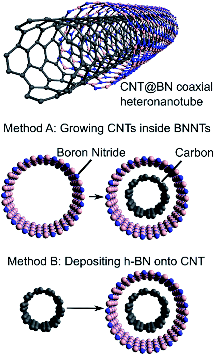 | ||
| Fig. 1 Schematic depiction of CNT@BN coaxial heteronanotube and methods of synthesis by (A) growing CNTs inside BNNTs or (B) depositing h-BN onto CNT. Only SWCNT and single layer h-BN are depicted here for simplicity. | ||
We also explore the motivations for synthesis of CNT@BN heteronanotubes by delving into the functionalities added to the CNT by the outer h-BN sheath. For example, h-BN acts as a thermally stable and chemically inert barrier against high temperature oxidation or as a dielectric barrier to electrically insulate individual CNTs.20 h-BN sheaths may also enhance the mechanical robustness and provide additional thermal conduction pathways along the CNT axis.21–23 The emergent properties of CNT@BN heteronanotubes lend to their proposed applications as reinforcement fillers in high temperature ceramic/metal matrix composites, energy dissipating devices, nanocables, high density interconnects, thermal interface materials, thermal management polymer composites and field emitters.
2 Synthesis and characterisation of CNT@BN
The two strategies towards synthesis of core–shell nanotubes of CNT@BN are by (a) growth of CNTs inside a BNNT or (b) deposition of coaxial h-BN onto the CNT surface, as summarised in Fig. 1. Each of these strategies, reviewed in Sections 2.1 and 2.2 respectively, present their own advantages and limitations. In Table 1, we compare the properties and accessibility of the CNT@BN hybrids synthesised by these two different approaches.| Characteristics | 2.1 Growing CNT inside BNNT (ref. 24–26) | 2.2 Coating h-BN onto CNT (ref. 20–23 and 27–41) |
|---|---|---|
| h-BN crystallinity | Highly crystalline BNNTs used; made by plasma arc discharge,42 laser vaporisation,43 or HTP44 | h-BN usually less crystalline; dependent on factors such as CNT surface crystallinity29 |
| h-BN number of walls | Single or double wall BNNTs used | Single or multi-wall concentric h-BN, or polycrystalline h-BN; controlled by deposition parameters |
| h-BN diameter restriction | <2 nm BNNT diameter needed to restrict C60 to coalesce | No restriction as deposited h-BN can encapsulate CNTs of variable diameter |
| CNT number of walls | Single-wall CNTs coalesced from C60 or restructured from amorphous C | Single or multi-wall; dependent on CNT source |
| CNT length | Short (e.g. ∼5 nm) SWCNTs ‘tubules’ formed by C60 coalescence or amorphous C restructuring | Variable; dependent on CNT source |
| Scalability | Microscope electron irradiation methods limited to small quantity of nanotubes; heat induced C60 coalescence more scalable | CVD, PVD techniques accessible to coat larger quantities of CNTs with h-BN |
2.1 Growing CNTs inside BNNTs
One route to producing a coaxial CNT@BN nanotube structure is by growth of the CNT inside a pre-formed BNNT. The BNNT acts as an encapsulating shell in which confined C60 fullerenes or amorphous carbon can be restructured into CNTs.Coalescence of C60 molecules into SWCNTs inside a BNNT was achieved by Mickelson et al., (2003)24 and Walker et al., (2017)25 by electron beam irradiation (120 keV) and heat treatment (1200 °C) respectively. In both cases, only BNNTs with a low diameter (<2 nm) could successfully restrict the fullerenes to fuse into SWCNTs. A crucial step to these methods is the introduction of C60 into the BNNTs, which requires opening the BNNT tips. This tip opening process, which involves BNNT air oxidation at 800 °C and/or hydrolysis with ammonium hydroxide solution, is necessary for facilitating C60 entry, but can also cause significant length reduction to the BNNTs, e.g. from ∼200 μm to ∼0.55 ± 0.22 μm.25 Consequently, the growing CNT's length dimension is also restricted by the BNNT template length.
Amorphous carbonaceous material trapped inside a single or double wall BNNT can also be restructured into a crystalline SWCNT by electron beam irradiation (80 keV), as demonstrated by Arenal et al., (2014).26 It appeared that a low concentration of carbon favoured crystallisation to a graphitic nanotube, whilst a high concentration of carbon was not crystallised during irradiation. The irradiation was also observed to shrink and cut the BNNT.
Notably, restructuring of carbon allotropes (C60 or amorphous C) into a SWCNT tends to result in multiple short (e.g. ∼5 nm), close ended SWCNTs that are encapsulated within the BNNT,25 rather than μm scale long, continuous SWCNTs. The combination of SWCNT ‘tubules’ sheathed by a BNNT is depicted in Fig. 2.
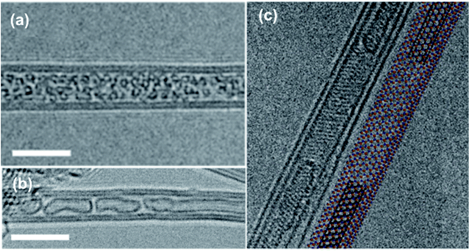 | ||
| Fig. 2 High resolution transmission electron microscopy (HRTEM) images of (a) C60 fullerenes encapsulated inside a double wall BNNT, followed by annealing at 1200 °C to form (b) SWCNT tubules grown inside BNNT. Scale bars are 5 nm. Reproduced with permission from ref. 25. Copyright 2017, Wiley-VCH. (c) Two capped SWCNTs tubules grown inside double wall BNNT via electron irradiation of amorphous carbon. Scale bar not given but inner CNT diameter is ∼1 nm. Reproduced with permission from ref. 26. Copyright 2014, American Chemical Society. | ||
2.2 Deposition of h-BN onto CNT
Both chemical and physical vapour deposition (CVD, PVD) techniques have been implemented to synthesise h-BN coatings on CNTs. PVD techniques involve the vaporisation of a solid target h-BN source to coat h-BN onto CNTs whilst CVD relies on decomposition and reaction of chemical precursors. CVD, further categorised into atmospheric pressure (APCVD), low pressure (LPCVD), autoclave and plasma assisted (PACVD), offers more control than PVD over the structure and crystallinity of the h-BN coating.The most often used method is APCVD involving the use of separate boron (boron oxide B2O3 or boric acid H3BO3) and nitrogen (nitrogen N2, ammonia NH3, urea CO(NH2)2) precursors. These precursor routes are adopted from economical industry methods for fabrication of h-BN.45 Other precursors explored in the variety of CVD techniques include boron trihalides (boron trichloride BCl3 and boron trifluoride BF3) with N2 or NH3, diborane B2H6 with NH3, and single source precursors borazine B3H6N3 or ammonia borane H3NBH3. The Fig. 3 pie plot summarises the PVD/CVD methods and associated precursors used to deposit h-BN on CNTs.
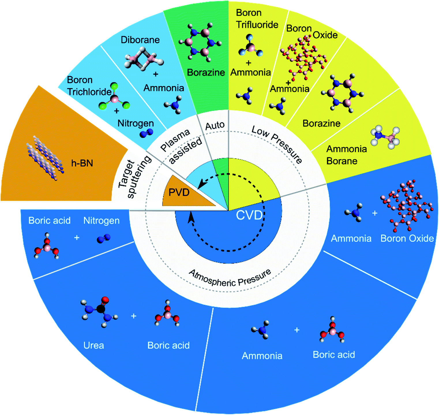 | ||
| Fig. 3 Summary of chemical vapour deposition CVD (atmospheric pressure, low pressure, autoclave and plasma assisted) and physical vapour deposition PVD precursor pathways used to deposit h-BN onto CNTs. Sections of the pie plot are proportionately allocated to represent the percentage occurrence of each method in the reviewed literature. Precursor structures are depicted as molecular or lattice compounds (the latter case for solid h-BN or boron oxide (B2O3)). | ||
Note that certain precursors present advantages with regard to ease of handling and storage. For example, boron trihalides, diborane and borazine are hazardous or produce harmful by-products, whilst ammonia borane is safe and non-hazardous.46 This safety and ease of handling aspect is one factor to consider when selecting amongst precursors, in addition to the quality of h-BN deposited.
In the following subsections, we review the structure-morphology and thickness (S2.2.1), crystallinity (S2.2.2) and purity (S2.2.3) of the h-BN coatings produced, associate them to the various h-BN deposition methods and emphasise controllability of these h-BN quality parameters.
2.2.1.1 Morphology. The ideal CNT@BN van der Waals heteronanotube consists of single crystal h-BN layer(s) forming an outer concentric BNNT shell that encapsulates the core CNT, as illustrated in Fig. 1. In reality, this ideal case has only been rarely achieved by deposition of h-BN onto CNTs.20 We thus categorised the morphologies of h-BN coating that have so far been synthesised. Generally, we found that the deposited h-BN coatings can be dichotomised into two descriptive categories: rough or smooth. Rough h-BN coatings are non-uniform and exhibit unevenness parallel to the surface of the underlying CNT.27,30,35,37 Smooth h-BN coatings are uniform and can range from highly crystalline20,29 to partially crystalline31,32,39 to polycrystalline.34,36,40 These two categories (rough vs. smooth) are visualised by transmission electron microscope (TEM) images of CNT@BN tubes synthesised by various deposition methods (Fig. 4).
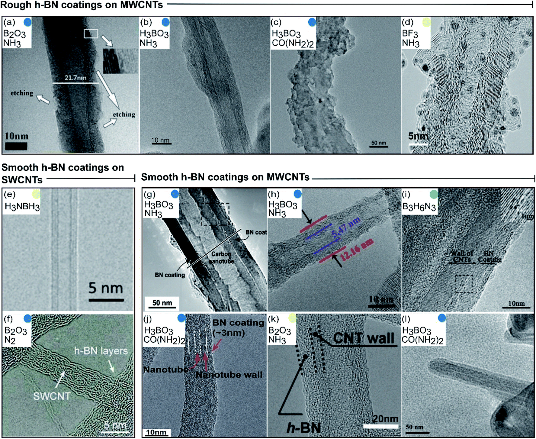 | ||
| Fig. 4 Catalogue of transmission electron microscopy images grouped according to morphology of the deposited h-BN coating. Colour codes are matched to types of CVD in Fig. 3 and precursor pathways are noted in insets. (a–d) Rough h-BN on MWCNTs. Reproduced with permission from ref. 27, 30, 35 and 37 Copyright 2015, American Chemical Society. Copyright 2011, Elsevier Ltd. Copyright 2014, Elsevier Ltd. Copyright 2018, American Chemical Society. (e and f) Smooth h-BN coatings on SWCNTs. Reproduced with permission from ref. 20 and 32 Copyright 2020, American Association for the Advancement of Science. Copyright 2015, Royal Society of Chemistry. (g–l) Smooth h-BN coatings on MWCNTs. Reproduced with permission from ref. 29, 31, 33, 34, 36 and 39. Copyright 2004, The American Ceramic Society. Copyright 2015, American Chemical Society, Copyright 2010, Elsevier Ltd. Copyright 2016, Royal Society of Chemistry. Copyright 2015, Wiley-VCH. Copyright 2008, Elsevier Ltd. | ||
Differences in CNT@BN structure amongst the various studies also exist in relation to the core CNT and h-BN dimensions, e.g. CNT diameter, number of CNT walls, and deposited h-BN thickness. Such structural properties for each of the studies reviewed here are summarised in Table 2.
| B precursor | N precursor | Carbon nanotube templates | h-BN coating | Ref. | ||||
|---|---|---|---|---|---|---|---|---|
| Type | Outer diameter (nm) | Wall thickness (nm) | Deposition time (min) | Temperature (°C) | Thickness (nm) | |||
| Atmospheric pressure CVD | ||||||||
| B2O3 | NH3 | MWCNTs | 15 | — | 60 | 1200 | 4–18 | 27 |
| MWCNTs | 20 | 2–3 | 240 | 1200 | 2 | 28 | ||
| H3BO3 | NH3 | MWCNTs | 100 | 18 | 50 | 1100–1200 | 15–20 | 29 |
| MWCNTs | 9.5 | 3 | 60 | 1027 | 1–2 | 30 | ||
| VA-MWCNTs | 8–9 | 1–2 | 60 | 900 | 2 | 31 | ||
| VA-MWCNTs | 8–9 | 1–2 | 60 | 900 | 1–2 | 21 and 22 | ||
| H3BO3 | N2 | SWCNT aerogel | 1 | — | 60 | 1000 | 1–3 | 32 |
| H3BO3 | CO(NH2)2 | MWCNTs | 25 | — | 180 | 1000 | 10 | 33 |
| MWCNTs | 9.5 | 3 | 180 | 900 | 3 | 34 | ||
| MWCNTs | 20–40 | <20 | 120 | 1000 | 10–25 | 35 | ||
![[thin space (1/6-em)]](https://www.rsc.org/images/entities/char_2009.gif) |
||||||||
| Low pressure CVD | ||||||||
| B2O3 | NH3 | VA-MWCNTs | <10 nm | 1–2 | 3 | 900 | 3–8 | 36 |
| BF3 | NH3 | VA-MWCNTs | 20 | 5 | 180 | 1100 | ∼5 | 37 |
| B3H6N3 | MWCNT aerogel | 12–13 | 3–4 | 30–120 | 900 | 2 | 38 | |
| H3BNH3 | SWCNT film | 1–2 | — | 180 | 1100 | 2–3 | 20 and 23 | |
|
||||||||
| Autoclave | ||||||||
| B3H6N3 | MWCNTs | 50–70 | ∼20 | 600 | 600 | <10 | 39 | |
|
||||||||
| Plasma assisted CVD | ||||||||
| BCl3 | N2 | MWCNTs | 8–12 | — | 1.5–4 | 650 | 3–8 | 40 |
| B2H6 | NH3 | VA-MWCNTs | 50 | — | 0.5 | 900 | 5–50 | 41 |
|
||||||||
| Magnetron sputtering PVD | ||||||||
| h-BN sputter target | VA-MWCNTs | 50 | — | 1–3 | Room | 15–30 | 41 | |
| h-BN sputter target | VA-MWCNTs | 50 | — | — | Room | 3–20 | 47 | |
The following sections describe in further detail the factors that influence h-BN coating thickness and crystallinity.
2.2.1.2 Thickness. The thickness dimension of the h-BN sheath is one of the structural parameter that can be controlled when depositing h-BN onto a pre-formed CNT. Thickness determines specific properties of the overall CNT@BN hybrid. Intuitively, thicker coatings of h-BN are more advantageous to protect the underlying CNT from structurally destructive processes such as oxidation or exfoliation during ultrasonication. Thicker h-BN coatings can also be a more effective electrically insulating barrier.20 In contrast, thinner layers, albeit more susceptible to damage, may be beneficial for other functions, such as improving field emission properties36,40 of the CNT@BN hybrids as discussed in Section 3.7.
Generally, the most common method of assessing the thickness of deposited h-BN is by measuring (from TEM images) the increase in nanotube diameter after coating the CNT. However, the h-BN thickness is often measured from a single or small, non-quantified number of tubes, leaving the question of whether the measurement is representative of the overall sample. Mohai et al., used an alternative means of thickness measurement, namely the Layers-on-Cylinder Model, which uses X-ray Photoelectron Spectroscopy (XPS) intensity data to calculate deposited h-BN thickness, but this has not been widely adopted.30,48,49
For the purpose of qualifying and comparing the time-efficiency of the various methods, we estimated the rate of h-BN deposition from the h-BN thicknesses and growth times reported in the literature, i.e. time within reactor at maximum temperature/plasma power etc. APCVD methods, the most studied, exhibit h-BN deposition rates in the range of 0.1 to 20 nm per hour. LPCVD methods were found to exhibit h-BN deposition rates between 1–160 nm per hour. Notably, PACVD40,41 and PVD41,47 techniques show deposition rates that are 2–3 orders of magnitude higher than other CVD techniques. These rates are summarised in Fig. 5.
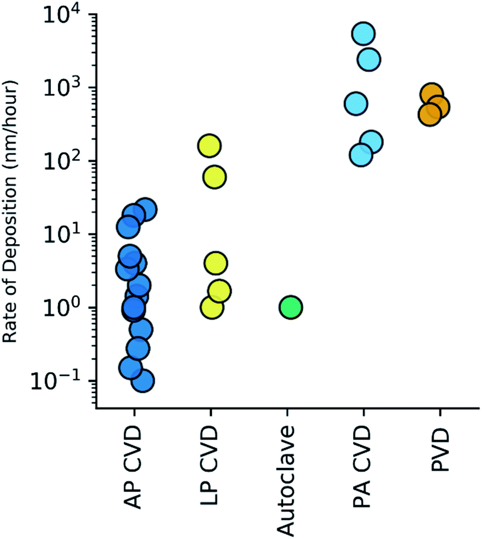 | ||
| Fig. 5 Calculated h-BN deposition rate (nm per hour) amongst the various methods of CVD (atmospheric pressure,21,27–35 low pressure,20,36–38 autoclave,39 plasma assisted40,41) and PVD.41 Rates are shown on a log10 scale. | ||
Whilst there appears to be trends in deposition rate amongst the different categories of CVD and PVD, control of h-BN deposition rate has also been proven possible within individual experimental setups. To change the h-BN deposition rate, certain parameters related to pre-reactor or in-reactor processes have been investigated in the literature.
An example of an in-reactor parameter change was demonstrated by Chang et al., (2015) who varied the gas flow rate of NH3/Ar at 100 sccm, 200 sccm and 300 sccm over a pulverised mixture of B2O3 and MWCNTs inside an atmospheric CVD system.27 After 1 hour at 1200 °C, h-BN coatings exhibited rough thicknesses (3–21 nm) (Fig. 4a) proportional to the flow rates implemented, demonstrating that a higher flow rate led to a higher h-BN growth rate.
A plasma assisted CVD study by Su et al., 2007 also implemented an in-reactor thickness control strategy.41 B2H6, NH3 and Ar were introduced at varying B/N flow ratios alongside a 50 W RF-plasma and 900 °C for a constant time of 30 s. A 4/1 ratio of B/N gas flow produced h-BN coatings of thickness 40–50 nm whilst lower ratios generated much thinner films on the MWCNTs.
The use of pre-reactor methods of treating the CNTs in order to vary the h-BN growth rate are more common, particularly amongst atmospheric CVD techniques that use aqueous state precursors (e.g. H3BO3 or CO(NH2)2).21,22,29,31–35,49 Such aqueous precursors are deposited onto the CNT surface, and this pre-coat is subsequently reacted in the furnace to form h-BN. Controlling the extent of the precursor coverage, for example by longer duration of infiltration,33affects the thickness of the final h-BN coating, thereby determining the effective h-BN growth rate.
However, a portion of CNT surface area is often limited from aqueous precursor access due to the CNT entanglement in agglomerates. Solution processing to de-tangle and disperse CNTs is used to obtain a more extensive, uniform precursor coating. These steps, often involving sonication and stirring, explain why APCVD methods that use aqueous precursors are overall much more time extensive (several hours to days) and non-gentle than most other methods for depositing h-BN.28,32,34 Additional procedures might include CNT functionalisation with hydroxyl and carboxyl groups to improve the dispersibility of CNTs in aqueous solutions.33–35,50
Surfactants have also been used to enhance CNT dispersibility, and to consequently enhance the h-BN growth rate.28,35 Li et al., (2014) investigated the effect of adding sodium dodecyl benzene sulfonate (SBDS) or polyvinyl pyrrolidone (PVP) to aqueous solutions of acidified MWCNTs in water/ethanol (1:1) solutions of boric acid and urea.35 After heat treatment to 1000 °C for 2 hours, only increasing SBDS content caused growth in h-BN coating thickness. This was attributed to SDBS surfactant improving dispersibility of the CNTs in the impregnation solution as well as facilitating adsorption of BO3− and NH4− onto the MWCNT surfaces. B and N sources were more concentrated on the nanotube surface, resulting in more h-BN formation in thicker layers. However, thicker layers appeared rough as depicted in Fig. 4c.
For CNTs that are individually separated on a substrate as part of an array, the problem of CNT agglomeration is no longer an issue.21,22,31,36,37,41 For example, Yang et al., (2015) deposited B2O3 onto MWCNTs in a vertically aligned array (VA-MWCNTs) by volatilizing it from a saturated solution of B2O3 in ethanol at 60 °C.36 When placed into the vacuum evacuated tubular furnace and heated to 900 °C in argon, the B2O3 melted, forming a molten coating that reacted with NH3 to form smooth but polycrystalline h-BN on the CNT surface (Fig. 4k). The h-BN thickness and estimated growth rate were effectively increased by extending the volatile B2O3 exposure time prior to furnace treatment.
Notably, when a single source gaseous precursor, such as borazine (Fig. 4i) or ammonia borane (Fig. 4e), is used to deposit h-BN, controlling h-BN thickness or growth rate is achievable mainly by altering growth time20,38 or reactor parameters. Despite there being no study to investigate the latter for h-BN grown on CNTs, Li et al., (2011) used direct pyrolysis of borazine to coat h-BN onto carbon fibres by CVD and highlighted that the rate of h-BN deposition was temperature dependent.51 A limited rate was influenced by either surface reaction mechanisms or mass transport controlling growth mechanisms. It was suggested that higher temperatures >1100 °C could favour gas phase nucleation, resulting in decreased h-BN deposition and less uniform coatings, albeit with higher crystallinity. These concepts are likely applicable to h-BN coating onto CNTs from single-source precursor routes.
For the studies that demonstrated amongst the fastest rates of h-BN deposition, h-BN growth rate was calculated to decrease over time. By Plasma assisted CVD, Morihisa et al., coated individual MWCNTs by introducing BCl3, N2 and H2 alongside a plasma with rf power 40 W.40 Su et al., used a PVD method with a radio frequency magnetron sputter source and a h-BN target.41 In both cases, several nm thick h-BN layers could be achieved within the timescale of seconds to minutes. The rate of deposition showed evidence of beginning to plateau within this time-scale.
Evident from the summary of h-BN thickness control is the range of thicknesses and deposition rates that have been achieved amongst the various methods in the literature. Future work can be informed accordingly if time-efficiency or method versatility for thickness control is a priority. However, thickness is just one descriptor of the h-BN coating and must be considered alongside other properties such as crystallinity and/or purity.
Generally, order/disorder of the h-BN layers can be interpreted locally from HRTEM images of individual nanotubes. Few studies conducted bulk analysis of the coating crystallinity, i.e. via X-ray diffraction (XRD), presumably because of insufficient sample quantity, thus being limited to electron microscopy. The most distinct diffraction peak for both graphitic carbon and h-BN is the (002) peak, followed by (100). As their respective (002) peak positions are slightly displaced from one another, specifically 2θ = 26.380 (JCPDS 41-1487) and 2θ = 26.748 (JCPDS 45-0896), one interpretation of XRD patterns for h-BN coated CNTs is that the (002) peak should be slightly upshifted and asymmetric relative to that of the pristine CNT.27,34,37,39
For a lamellar structure such as h-BN, a highly ordered crystal will have both two- and three-dimensional ordering. As the structure becomes more crystalline, the XRD pattern shows characteristic upshift and narrowing of the (002) peak, alongside the appearance of higher resolved peaks e.g. (101), (102), (004), (110), (112) etc. Otherwise, the BN is in fact not fully ordered h-BN but is instead turbostratic BN (t-BN); the layers may be parallel but are randomly stacked along the c-axis.55 See Fig. 6.
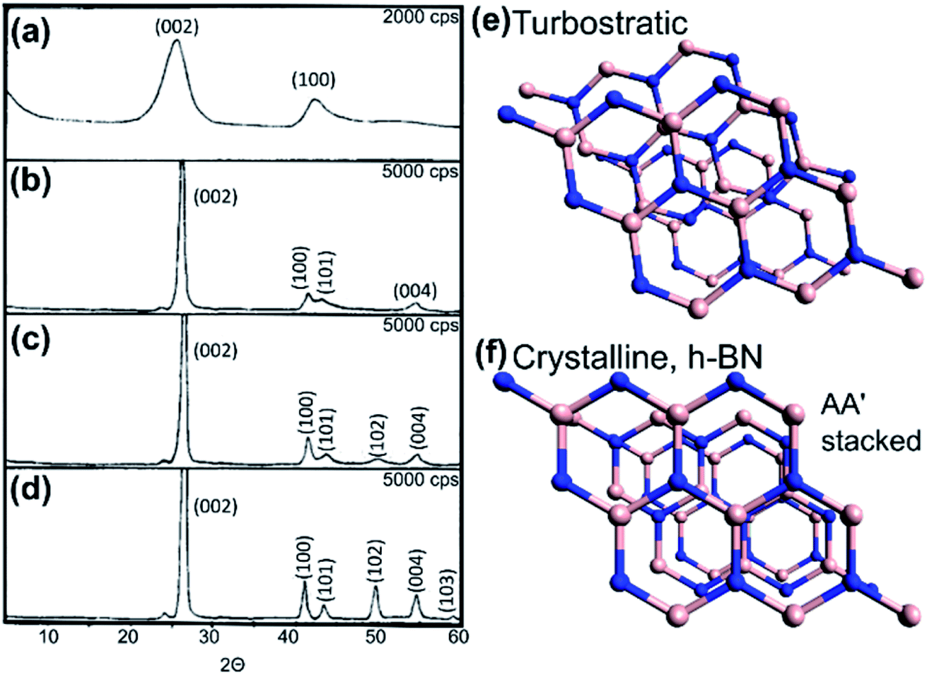 | ||
| Fig. 6 (a–d) X-ray diffraction patterns of h-BN with increasing crystallinity from turbostratic to crystalline forms. Reproduced with permission from ref. 55. Copyright 1962, American Chemical Society. (e) Model of turbostratic BN with random alignment along the c axis. (f) Perspective model of crystalline h-BN whereby B and N atoms are superposed on each other in succession (AA′ stacked) along the crystal c-axis. | ||
Few studies also used Raman spectroscopy to make the observation that the underlying CNT structure was not affected by the BN coating process.21,31,32,36 Pristine MWCNTs exhibit most distinctly the Raman D band (∼1350 cm−1) and G band (∼1582 cm−1), which are disorder-induced and in-plane vibration of sp2 carbon induced respectively.56 Thus maintenance of the G band and the D/G intensity ratio can indicate a preserved graphitic structure of the core CNT. The distinct E2g mode for h-BN due to in plane vibrations is exhibited at 1366–1370 cm−1 for bulk h-BN.57,58 Due to the closeness of the D and E2g peaks for graphite and h-BN, the E2g band for h-BN coated MWCNTs is often not noticeable. However, in a small number of cases, it was possible to deconvolute the D + E2g peaks to show the core–shell contributions made by carbon and boron nitride respectively.27,37,38
2.2.2.1 Rate of h-BN deposition effects on crystallinity. A general observation on h-BN coating crystallinity variance is that methods which deposit h-BN at a high rate tend to produce polycrystalline or amorphous h-BN. This is demonstrated using PACVD,40,41 which has high rates of deposition from 100 to 10
000 nm h−1 (Fig. 5). Su et al., suggested that h-BN coatings synthesised by sputter deposition (PVD) have even higher defect densities than h-BN produced by plasma assisted CVD.41 At a similarly high deposition rate, Yang et al., also produced polycrystalline films when using a low pressure CVD method (Fig. 4k).36
2.2.2.2 CNT surface crystallinity effects on h-BN crystallinity. A small lattice mismatch of h-BN and graphitic carbon (1.7%) indicates the potential for epitaxial growth of h-BN on the CNT surface.59,60
Chen et al., (2004) investigated the influence of surface crystallinity of starting CNT on the crystallinity of the deposited h-BN layers.29 The MWCNTs used were either pyrolytically stripped (PS-CNTs) for an etched, disordered and turbostratic surface or heat treated to 3000 °C (HT-CNTs). These MWCNTs, infiltrated with H3BO3, were subjected to 1100–1200 °C heat in a horizontal quartz tube furnace with NH3 flow. The result was that PS-CNTs had a rough, polycrystalline h-BN coating whilst the HT-CNTs appeared to be encapsulated by a uniform cylindrical h-BN tube, as shown in Fig. 7. The difference in quality of coating on the PS-CNTs versus the HT-CNTs was attributed to the difference in surface structure of the CNTs; a disordered surface would facilitate multiple h-BN nucleation sites whilst an ordered surface has rarer nucleation. Thus, the difficulty of h-BN nucleation on a highly crystalline CNT surface facilitates single crystal h-BN growth rather than polycrystalline growth.
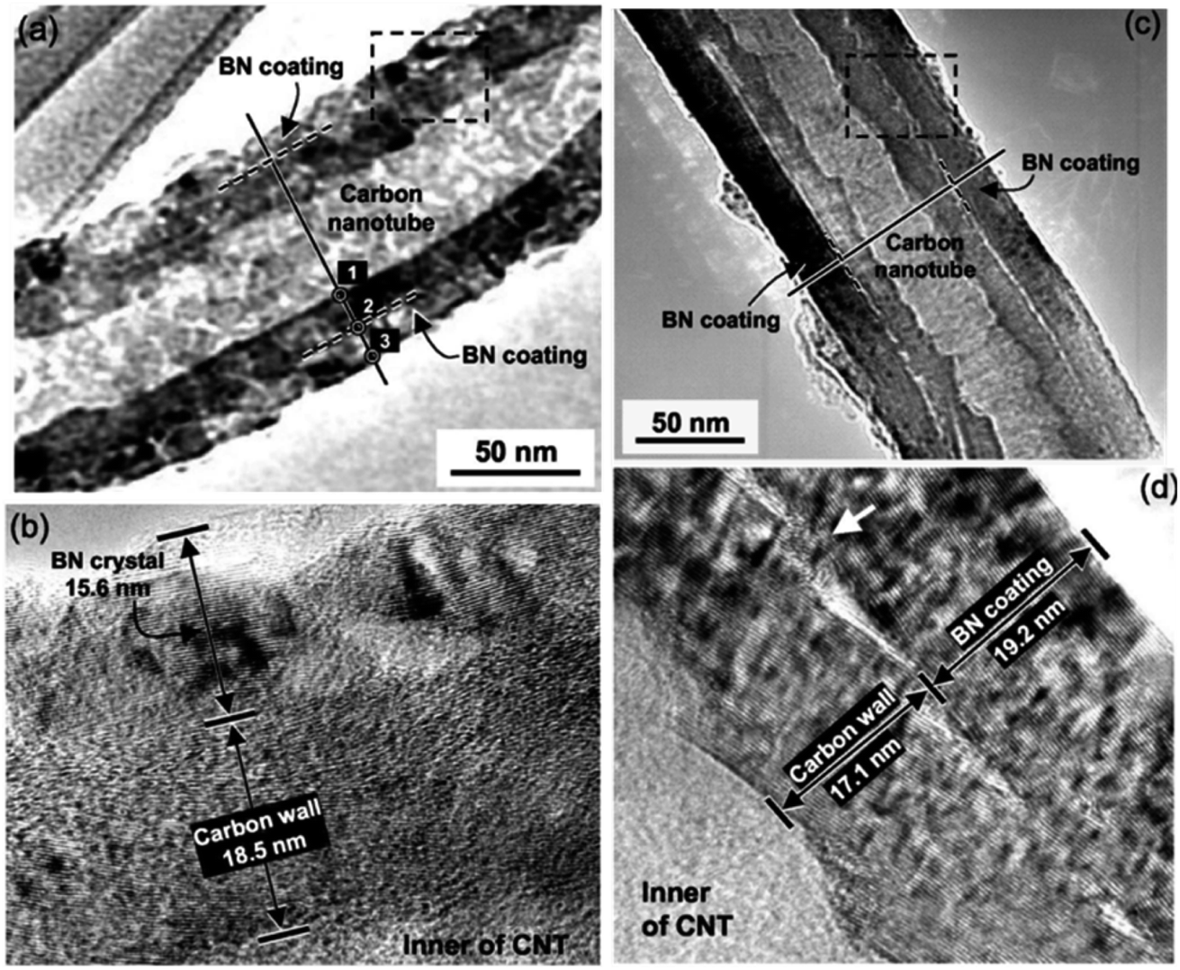 | ||
| Fig. 7 (a and b) TEM and HRTEM images of rough, polycrystalline h-BN coating formed on pyrolytically stripped MWCNT. (c and d) TEM and HRTEM images of smooth, crystalline h-BN coating formed on heated treated (3000 °C) MWCNT. Surface crystallinity of the MWCNT influences the h-BN coating crystallinity. Reproduced with permission from ref. 29. Copyright 2004, The American Ceramic Society. | ||
This finding elucidates the importance of the CNT surface structure on the quality of the h-BN coating formed and this can be extrapolated to all CVD coating studies. Noteworthy is the inevitable wide range of CNT starting material as summarized in Table 2, which introduces a non-constant variable laterally across the literature. Most CNTs used are not perfectly crystalline. Given that variably sourced CNTs will present different degrees of surface order/disorder, the resultant h-BN coating on two separate CNT types could potentially be dissimilar even after the same coating procedure.
2.2.2.3 Temperature effects on h-BN crystallinity. A higher growth temperature of h-BN is expected to produce more crystalline layers. A study by Li et al., (2011) showed the temperature dependence of h-BN coating crystallinity for BN coats grown on carbon fibre from borazine pyrolysis.51 From 900–1100 °C, the crystallinity improved from t-BN to h-BN, as characterised by the differing XRD patterns, which showed higher resolved peaks appearing in the more crystalline structure.
Temperatures in the range of 600–1200 °C have been explored for synthesizing h-BN onto CNTs. When considering the XRD patterns from the few studies that utilized this bulk characterisation technique, only Chang et al., reported higher resolved peaks for the (101) reflection of h-BN coated onto CNTs, suggesting the presence of more 3-dimensional ordering in the h-BN coating.27 The higher growth temperature (1200 °C) is a likely contributing factor to this. Other studies tended to only observe the (002), (100) and (004) peaks for synthesis temperatures at 600 °C,39 900 °C34,38 or 1100 °C,37 indicating a more turbostratic h-BN structure. However, these crystallinity results cannot be solely associated with temperature, as other factors also influence the h-BN crystallinity as discussed herein, including the CNT template surface crystallinity, h-BN deposition method etc. Whether a certain precursor pathway is more favourable for synthesizing more crystalline h-BN is left to be explored.
2.2.2.4 Single crystal SWCNT–BNNT & chirality independence. Xiang et al., have been the first to synthesize SWCNT–BNNT coaxial single crystals, by deposition of 1–8 layers of h-BN onto pristine SWCNTs in a low pressure CVD system (Fig. 4e).20 Here, characterisation of nanotube crystallinity was achieved by nano-area electron diffraction, which revealed the perfect crystallinity of the SWCNT and BNNT layers.
An open edge growth mechanism of the BNNTs caused the occurrence of atomic steps along individual nanotubes, leaving regions of exposed SWCNT. It was thus possible to assign chiralities to the SWCNT and BNNT belonging to the same van der Waals heteronanotube. No apparent chiral angle dependence was observed between the SWCNT and BNNT sheath. This is a significant difference when compared to 2D graphene–h-BN heterostructures, which exhibit symmetry and alignment between layers.
X-ray photoelectron spectroscopy (XPS) is often used to investigate the elements present within a sample of nanotubes by a survey scan,30,38,49 and high resolution XPS spectra can be deconvoluted to investigate bond speciation within heteronanotubes.27,28,31–35,39,50
Accurate interpretations of CNT@BN XPS spectra, particularly regarding the assignment of bond types to deconvoluted peaks, must be informed by an understanding of XPS principles. Binding energies (BE) depicted in XPS spectra refer to that of core-level electrons bound to an atomic nucleus. Incident X-ray photons with sufficient energy to overcome the BE can eject these core-level electrons (now photo-electrons), which are collected and sorted by kinetic energy to calculate their original BE. When atoms are involved in chemical bonding, core-level electron BE is also altered due to changes in electron density and coulombic interaction effects.61 This has implications for detecting the chemical state of a photo-electron emitting atom. For instance, B atoms have core-level 1s electrons with BE dependent on the x species in B–x bonds, e.g. B–C, B–N etc. As the electronegativity of species x increases, so does the BE of the B1s electrons, such that deconvoluted XPS peaks in a B1s spectra can be assigned in the BE coordinate order B–C < B–N < B–O (e.g.Fig. 8). The same applies for C–B < C–C < C–N and N–B < N–C etc. in C1s and N1s XPS spectra respectively.62 Another aspect of CNT@BN XPS interpretation often overlooked is the asymmetrical fitting of the C1s graphitic carbon sp2 contribution.63
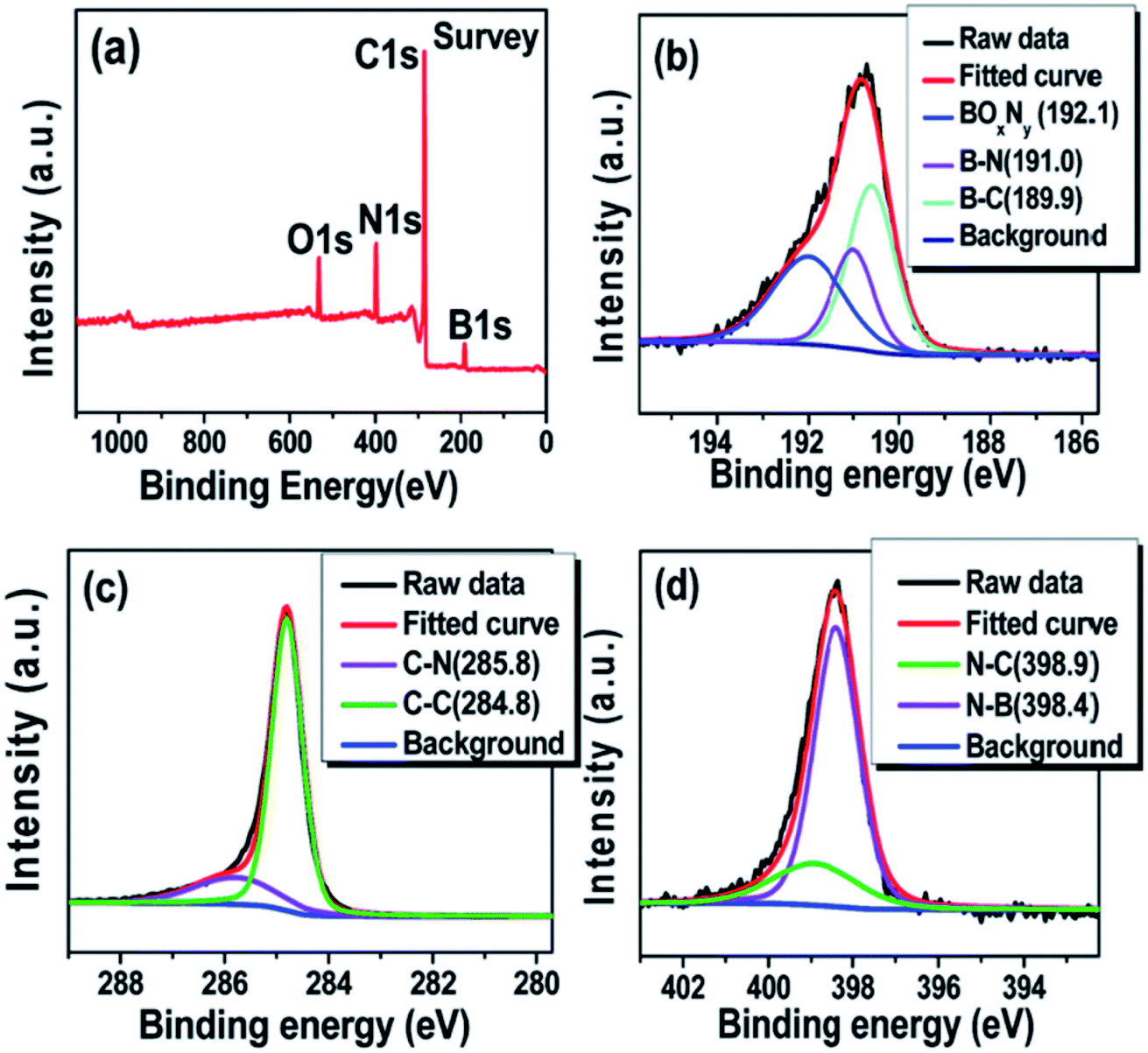 | ||
| Fig. 8 Example of XPS spectra that are deconvoluted to show B–N, B–C, C–N, C–C etc. bonds for a h-BN coated MWCNT synthesized via a B2O3 + NH3 pathway using H3BO3 and CO(NH2)2 as starting precursors. (a) XPS survey spectrum (b–d) High resolution spectra of B1s, C1s and N1s respectively. Reproduced from ref. 34 with permission from the Royal Society of Chemistry. | ||
Other spectroscopic techniques such as energy dispersive X-ray spectroscopy (EDX) and electron energy loss spectroscopy (EELS) are especially valuable in confirming the spatial distribution of B, N and C. EELS is more effective at showing the core–shell structure of the hybrids by element maps27,28,31 or line scan profiles.29 EELS spectra can also indicate sp2 type bonding based on the π* peaks on the B–K, C–K and N–K edges.28,29,36 Further detail about bonding configuration within the layers of the nanotube can be explored by collecting high resolution spatially resolved EELS spectra, so as to analyse the electron energy loss near edge structures (ELNES). Studies on heteroatomic BxCyNz nanotubes have examined ELNES to identify different types of N–C bonds (e.g. graphitic, pyrrolic etc.) from features on the π* peak of the N–K edge.19,64 However, ELNES investigation has not yet been applied amongst the studies discussed here to spatially resolve the occurrence of B–C or N–C type bonds.
2.2.3.1 Non-carbon impurities. Besides XPS and EELS, FTIR can also be used to prove the presence of h-BN and potentially to detect non-B–N bonds. The two IR active modes of h-BN are due to B–N in plane stretching and B–N–B out of plane stretching. Some studies identify FTIR peaks ascribed to the graphitic carbon.21,22,31 B–C or N–C bonds detected by FTIR in ternary boron carbonitride nanotubes, at 1171 cm−1 and 1279 cm−1 respectively,68 have not been reported for CNT@BN nanotubes. Oxygen related impurities detected by FTIR are discussed in Section 2.2.3.1.
Jeong et al., also implemented Raman to detect non-BN bonds formed in their h-BN coated SWCNT aerogels (Fig. 4f).32 A peak at 1490 cm−1 was attributed to C–N bonds, whilst at lower Raman shifts corresponding to the radial breathing modes of SWCNT, a peak below 200 cm−1 was deemed to be from B–C bonds.
2.2.3.2 h-BN/C covalent hybridisation dependence on precursor pathway. The B2O3 + NH3 precursor pathway for deposition of h-BN onto CNTs promotes the formation of covalent B–C and N–C bonds. This is also applicable to variants of this pathway, including H3BO3, that is dehydrated to B2O3 at elevated temperatures in the reactor,29 and CO(NH2)2, which decomposes in situ to NH3.33
The reaction of B2O3 and NH3, the so called ‘amide route’ (reaction (1)) is thermodynamically less favourable than reaction (2), the carbothermic reduction of B2O3.2,29 h-BN formation occurs preferentially with the involvement of C from the CNT itself, which acts a B2O3 reducing agent (reaction (2)).
| B2O3 + 2NH3 → 2BN + 3H2O | (1) |
| B2O3 + 3C + 2NH3 → 2BN + 3CO + 3H2 | (2) |
| B2O3 + 2C + 2NH3 → 2[BN–C] + 3H2O | (3) |
A consequence of reaction (2) is the ‘etching’ of the underlying CNT, whereby the CNT structure is altered by the removal of C atoms.27,49 These C atoms are removed as a gaseous oxide or are incorporated into the growing h-BN layers, as in reaction (3). Reaction (3) is often referenced as a means of substituting C with h-BN to form ternary BxCyNz hybrid nanotubes.68–70
According to Chang et al., the outermost h-BN layers synthesized from the carbothermal process have fewer B–C or N–C bonds and are primarily h-BN.27 This is because the first few ternary B–N–C layers formed prevent further reaction of the underlying CNT, so any additional h-BN formation can only proceed following reaction (1). Radial phase separation of carbon and h-BN, caused by atom diffusion to minimize the occurrence of unstable bonds,16–19 may also explain why the layers grown by reaction (3) are not homogeneous BxCyNz. Bond stability increases in the following order:19 C–B (2.59 eV) < C–N (2.83 eV) < C–C (3.7 eV) < B–N (4 eV).
Other precursor pathways, particularly involving single source precursors such as borazine or ammonia borane, may be more viable for the deposition of h-BN without the formation of covalent B–C–N interactions with the underlying CNT. For example, Xiang et al., found no evidence of B–C or N–C bonds in their highly crystalline h-BN deposits synthesized by the decomposition of ammonia borane; the SWCNT–BNNTs synthesized were true van der Waals hybrids (Fig. 4e).20
In summary, the selection of a specific precursor(s) for h-BN deposition onto CNTs requires careful consideration of precursor effects on the final structure and bond composition of the CNT@BN nanotube.
Oxygen impurities have been reported in multiple studies on CNT@BN heteronanotubes. Precursor pathways utilising H3BO3 or B2O3 as the boron precursor present a predictably greater likelihood of leaving residual oxides or oxynitrides in the CNT@BN sample.27,34,35
Other sources of oxygen have been attributed to physicochemically adsorbed oxygen28,50 or adsorbed water molecules, the latter often detected as hydroxyl groups by FTIR.21,22,31,38,50
Further understanding of the types and role of oxygen impurities on the properties of the CNT@BN heteronanotubes is required.
3 Applications and properties
This section reviews the properties of CNT@BN (Fig. 9) with a focus on its application potential, as summarised in Fig. 10.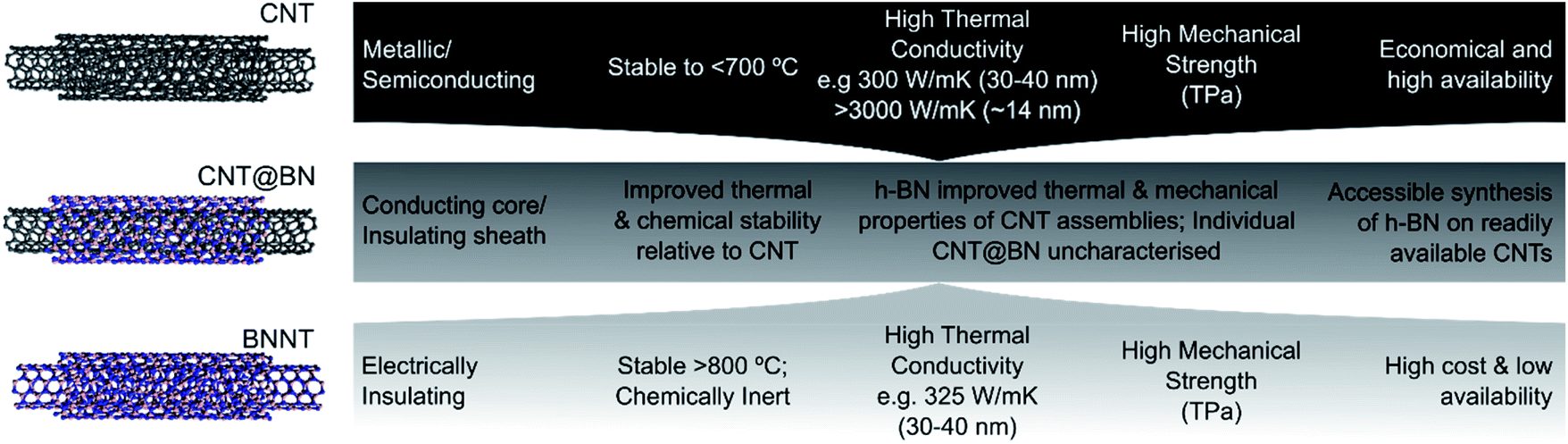 | ||
| Fig. 9 A comparison of the main properties and availability of CNT@BNs, pure CNTs and BNNTs. See previous reviews for more detailed comparisons of CNTs versus BNNTs.65–67 | ||
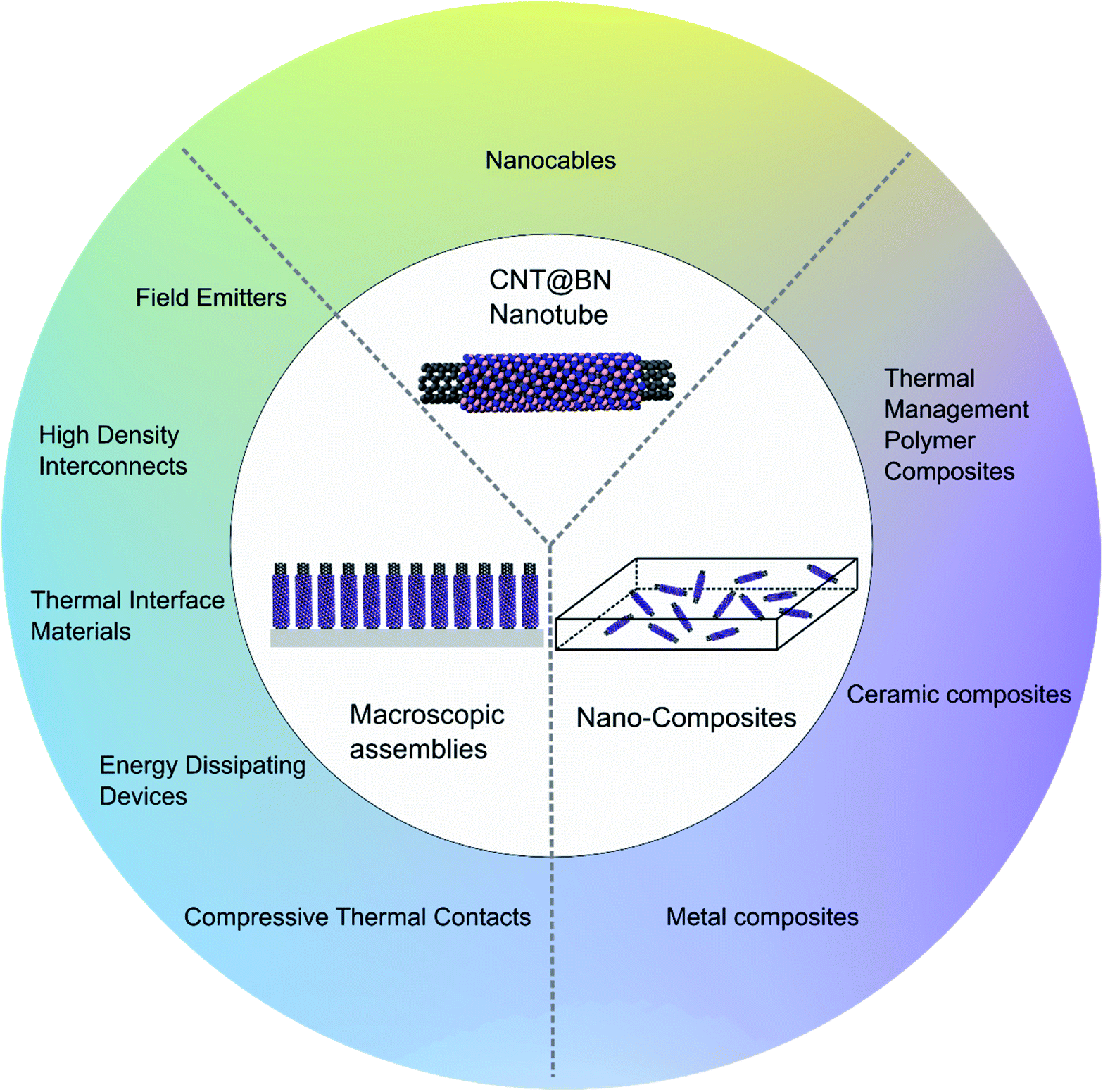 | ||
| Fig. 10 Summary of some potential applications of CNT@BN heteronanotubes as individual nanotubes, macroscopcic arrangements or nano-composites. | ||
3.1 High temperature composite reinforcement fillers
To improve the mechanical properties of metal or ceramics, they can be reinforced with high aspect ratio fillers with exceptional mechanical properties. CNTs, which exhibit a high Young's modulus and tensile strength,71 have been considered as novel reinforcement fillers in metal/ceramic matrices to enhance toughness, stiffness, wear or fatigue resistance.72 However CNTs begin oxidising in air at ∼500–700 °C (depending on their crystallinity),73–76 thereby losing their structural integrity. High temperature structural composites require more thermally stable reinforcement fillers. The filler nanotubes should also be chemically inert at the elevated temperatures to prevent formation of undesired bonds, e.g. metal–carbide interfaces, that can weaken the composite,77 as can happen when CNTs are used in metal matrix composites.Introducing h-BN on the surface of graphitic carbon offers protection of the carbon against oxygen attack at elevated temperatures, as illustrated in Fig. 11. For example, a study of oxidation resistance of graphene revealed that in its pristine state it was stable until 700 °C, whereas if the graphene was coated with h-BN, oxidation was delayed till 1000 °C.78 h-BN nanotubes (BNNTs) exhibit high oxidative stability, with reported onset oxidation temperatures at 830 °C,79 900 °C80 and 1000 °C,81 also dependent on crystallinty.52,80
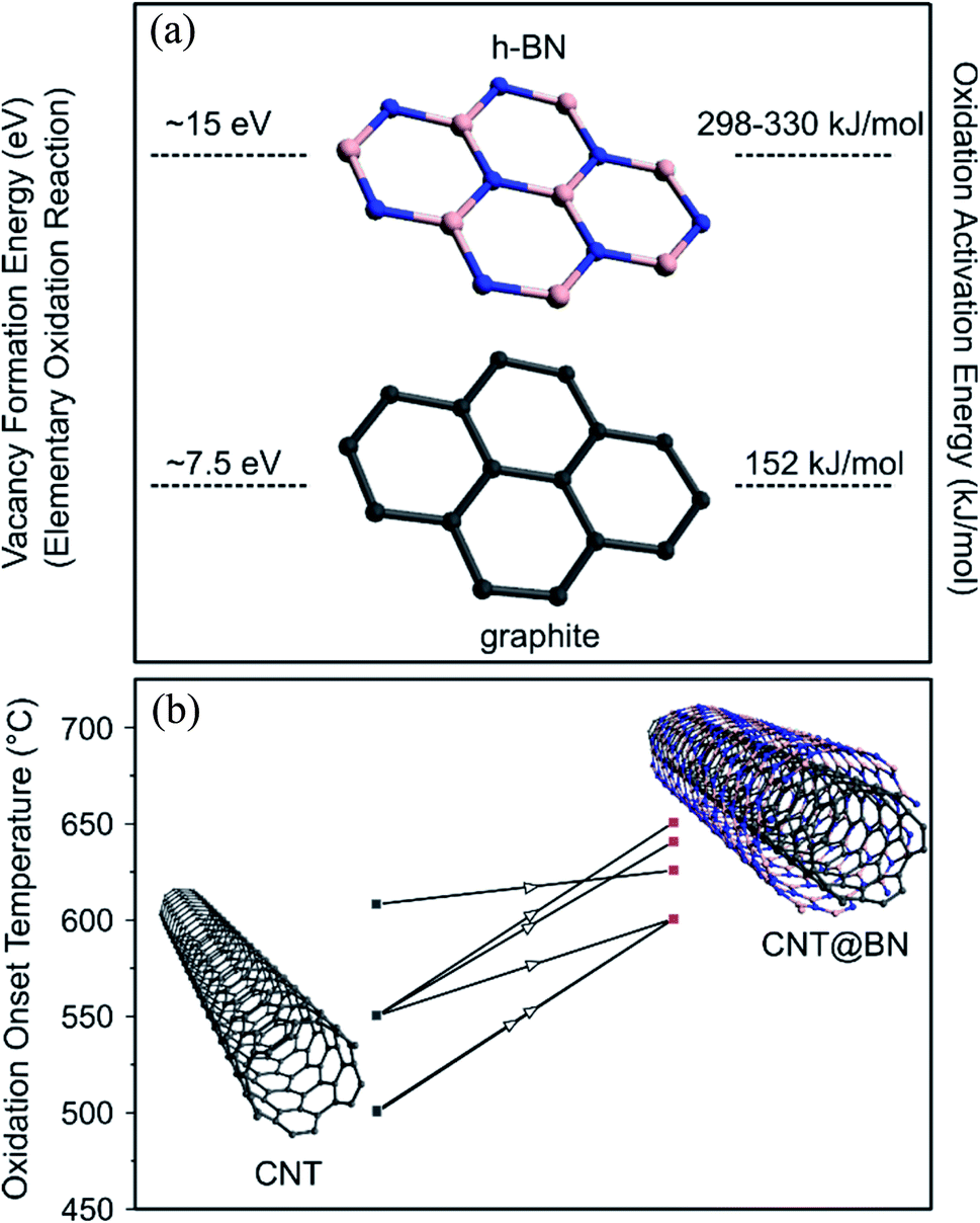 | ||
| Fig. 11 (a) Vacancy formation energy78,83 and oxidation activation energy52 of h-BN vs. graphitic carbon, justifying why h-BN is more oxidatively stable at high temperatures that graphitic carbon. (b) Compiled oxidation onset temperature values from studies that reported TGA results on CNTs prior to h-BN coating and after h-BN coating,21,27,30,31,39,50 suggesting that h-BN was effective at improving oxidation resistance. | ||
As h-BN is chemically inert, it can prevent the formation of undesired matrix-filler bonds. h-BN coats have been implemented on larger dimensional carbon fibres generally for the purpose of improving oxidation resistance and preventing bonding between the reinforcing fibre and a ceramic matrix.51,82
Accordingly, in the nanotube form, an outer h-BN coating on CNTs should offer the advantages of improved oxidative and chemical stability. To investigate the former, thermogravimetric analysis (TGA) of MWCNT@BN hybrid nanotubes in air or oxygen rich gas flows was conducted in several studies.21,27,30,31,38,39,50 The oxidation onset temperature of MWCNT@BN was found to be increased relative to pristine MWCNT, by up to 100 °C in some studies. Furthermore, considerable residual weight percentages (ca. >50%) have been recorded at 800–1100 °C, pointing to the improved oxidative stability of MWCNT@BN.
h-BN has characteristically higher thermal oxidation resistance than graphite because of the larger activation energy barrier for oxidation to occur. The oxidation reactions for graphitic carbon and h-BN are as follows:
| C + O2 → CO2 | (4) |
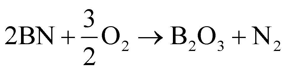 | (5) |
The elementary oxidation reaction of carbon requires the formation of a sole vacancy in a graphitic lattice while multiple B and N vacancies must be formed for the elementary oxidation of h-BN. The initial vacancy formation energy (Hvac) for carbon is 7.5 eV83 and the estimated Hvac for two BN divacancies is at ∼15 eV.78 Empirically measured oxidation activation energies for highly graphitized carbon and commercial h-BN were found to be 152 kJ mol−1 and 298–330 kJ mol−1 respectively.52
Whilst pure BNNTs are considered good candidates as reinforcement fillers, and have been tested in Al2O3,84 aluminium85 and titanium86 matrices, they are available in low quantities and at high cost relative to CNTs. Therefore, a feasible and economically favourable alternative is to introduce the benefits of h-BN by coating it onto CNTs.
Beyond the improvement in oxidation resistance offered by the h-BN coating, which maintains the CNT@BN nanotube structural integrity at higher temperatures, the mechanical robustness of the nanotube is also altered by the h-BN outer layer, as further discussed in Sections 3.2 and 3.3.
3.2 Energy dissipating devices
Non-linear elastic materials are of interest for use in energy adsorbing applications for mechanical cushioning, compliant coatings/membranes, structural materials undergoing cyclic stress and devices to dissipate shockwaves, acoustics and vibrations etc.21,87–89VA-CNT arrays that exhibit spring-like behaviour after buckling and folding from compressive stress have been considered for such applications, as the processes of nanotube deformation and inter-tube friction allow for energy dissipation.87–89
However, Jing et al., (2016) showed that at high uniaxial compressive strain (90%), VA-CNTs (<10 nm diameter CNTs) underwent almost complete plastic deformation.21 By introducing 2–5 walls of h-BN coating onto the CNTs (with similar structure as in Fig. 4h), the array exhibited shape recovery to as much as 77% for the same compressive strain, and showed enhanced cyclic compressibility performance as 76% shape recovery occurred after 10 cycles. See Fig. 12 schematic. Compression strength was also observed to increase from 0.47 MPa to 2.47 MPa for the VA-CNT and VA-CNT@BN arrays respectively.
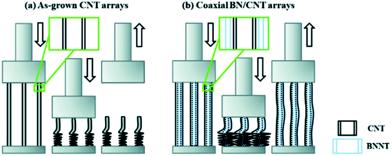 | ||
| Fig. 12 Illustration that coating of h-BN onto VA-MWCNTs changed mechanical response to compression. (a) Pristine MWCNTs underwent plastic deformation upon compression. (b) BN coated MWCNTs with 3-walls of BN exhibited elastic recovery. Reproduced from ref. 21 with permission from the Royal Society of Chemistry. | ||
The h-BN coating improved the mechanical robustness of the array and maintained its high energy dissipation ratio throughout cyclic stress. The h-BN also presented an oxidation resistant barrier to protect the CNTs from oxidation induced structural weakening. The thicker coated h-BN samples that were annealed to 400 °C in air retained their mechanical properties at 50% strain.
Similarly, h-BN coated onto SWCNT aerogels enhanced elasticity.32 The random oriented SWCNT network in the aerogel experienced plastic deformation at just 10% compressive strain but with the h-BN coating, this limit increased to 60%. Young's Modulus increased by 100% relative to the pristine SWCNT aerogel.
Several in silico studies have probed the mechanical performance of SWCNTs with a single coaxial layer of h-BN,90–93 but empirical measurement of an individual CNT@BN nanotube's mechanical behaviour remains to be conducted.
3.3 Nanocables
The primary components of an electrical cable are a core electrically conductive wire sheathed by insulating material. At the scale of nano-electronics, an individual metallic CNT can behave as the conductive wire, but requires an equally nanoscale insulator to prevent against current leakage and to provide environmental protection.Nano-cables consisting of a metallic SWCNT sheathed in coaxial h-BN have been proposed,94–96 as h-BN has a stable wide band gap, is structurally compatible with the core CNT and can provide a barrier against oxidation at elevated temperatures.
In silico studies have highlighted the effectiveness of CNT@BN as a nanocable. For example, DFT modelling of a coaxial CNT@BN nanocable, with chiralities (5,5)C@(17,0)BN, demonstrated that the core and sheath retained their separate electronic natures up to ∼3500–3700 K94 and under tensile deformation.95 Zhang et al., (2007) also pursued the concept of a nanocable by ab initio calculations.96 Band structure of the independent components remained unchanged when ±5% uniaxial strain was applied. Calculations also suggest the hybrid nanocable can survive 500 GPa of radial deformation. As such, the h-BN sheath satisfied criteria of being lightweight, insulating and contributing toward robustness of the nanocable, making it more suitable for application in nanoelectromechanical systems.
Realisation of the nanocable application of CNT@BN will require fine control and bulk scale standardisation of CNT@BN structure. Positioning of these nanocables within devices will also demand very precise manipulation at the nanoscale.
3.4 High density interconnects
Printed electronic circuit boards (PCBs) with a multi-layer architecture have vertical access interconnects (vias) that act as conductive pathways between layers. CNTs, which carry large currents (109 A cm−2) have been proposed to replace metal based vias, the latter which are more vulnerable to electromigration and thermal failures.97VA-CNT arrays provide a dense bundle of conductive channels that act collectively to increase conductivity of vias. Current directionality is a priority for vias and current leakage in the transverse direction of the VA-CNT array is undesired.97
To reduce transverse conduction within the CNT array, Zou et al., (2019) proposed infiltration of VA-CNT with h-BN.37 The resulting VA-CNT@BN array exhibited highly anisotropic electrical conductivity (i.e. 1060.43 S m−1 parallel to the lengthwise direction of VA-CNTs and 4.43 S m−1 perpendicular to the VA-CNTs) because of the electrically insulating effect of h-BN present at the contacts between adjacent CNTs. In this study, the morphology of the h-BN coating was unique, as depicted in Fig. 4d.
This proposed application opens up a new path of research for CNT@BN heteronanotubes as components in integrated circuits and printed circuit board electronics components.
3.5 Thermal interface materials (TIMs)
Waste heat generated from electronics components must be dissipated to prevent negative effects on performance and reliability. Effective thermal management solutions are increasingly important for miniaturized electronics which have high power density components that generate distinct hot-spot regions.98One bottleneck of heat conduction in electronics devices is often at the interface between two materials/layers, where there are air gaps. Thermal interface materials (TIMs) fill these gaps and enhance the thermal conductance between the mating surfaces.99
VA-CNTs arrays have been considered for application as TIMs as CNTs exhibit exceptionally high thermal conductivity along the nanotube axis.99,100 For example, MWCNTs with diameters 14 nm showed 3000 W m−1 K−1 conductivity.101,102
Despite the high thermal conductivity of individual CNTs, macroscopic arrangements tend to exhibit significantly reduced thermal transport properties. This can be due to factors such as phonon scattering arising from defects in the tubes and/or low nanotube volume fraction, as the presence of thermally resistant air within the array can lessen the overall conductivity.103
Jing et al., (2017) used h-BN coatings to enhance the thermal transport properties of a VA-CNTs array, as depicted in Fig. 13.22 With the 4–5 layers of h-BN coating, the κ value for the CNT array increased from 15.5 W m−1 K−1 to 29.5 W m−1 K−1.
 | ||
| Fig. 13 Scanning electron microscopy (SEM) images of (a) VA-MWCNTs and (b) VA-MWCNTs coated in h-BN. The h-BN coating increased thermal conductivity of the aligned assembly from 15.5 W m−1 K−1 to 29.5 W m−1 K−1. Reproduced with permission from ref. 22. Copyright 2017, American Chemical Society. | ||
The h-BN proved an effective infiltrating material for the CNT array since (i) it can reduce the array air fraction because of radial thickening from the h-BN coating, (ii) the CNT maintains its original thermal conductance and (iii) the h-BN itself is equally an excellent heat conductor that adds additional pathways for heat conduction.23,104
CNT@BN heteronanotubes offer a highly promising alternative to pure CNT assemblies as TIMs. However, although Jing et al., demonstrated a ∼50% improvement in thermal conductivity of their VA-CNTs subsequent to h-BN coating, a much greater increase on the order of several magnitudes is still necessary to meet the urgent demands of the electronics industry. Future work must explore ways of optimising thermal conductivity in macroscopic assemblies of CNT@BN heteronanotubes.
3.6 Thermal management polymer composites
Polymers form an important class of materials in electronics packaging for use in substrates, encapsulants, adhesives, heat spreaders and heat sinks etc. Passive thermal management from packaging materials requires that the polymer-based materials are thermally conductive.105The addition of thermally conductive nanotube fillers to a polymer matrix can create a conductive network, thereby making a thermally conductive polymer nano-composite.98 Whilst CNTs have been considered as filler materials for this purpose, they are inherently also electrically conductive. To prevent short-circuiting, passive polymer based components must be electrically insulating if they are located in the close proximity of electrically active components. Therefore, ideal thermally conductive filler material should not be electrically conductive.105
Yan et al., (2014) proposed the use of h-BN coated MWCNTs (depicted in Fig. 4j) as fillers in a polyimide (PI) matrix, to form thermally conductive, electrically insulating nano-composite films.34 The MWCNTs were coated with h-BN prior to feeding into the polymer matrix. The nano-composite samples with MWCNT@BN filler had both surface and volume electrical resistivities that were significantly higher than those with un-modified MWCNTs (see Fig. 14). The volume resistivities for pure PI, PI + MWCNT and PI + MWCNT@BN were 3.7 × 10¹⁴ Ω cm, 6.82 × 10⁷ Ω cm and 7.69 × 10⁹ Ω cm respectively for 3 wt% filler, i.e. resistivity is two orders of magnitude different between composites with the coated and uncoated MWCNTs.
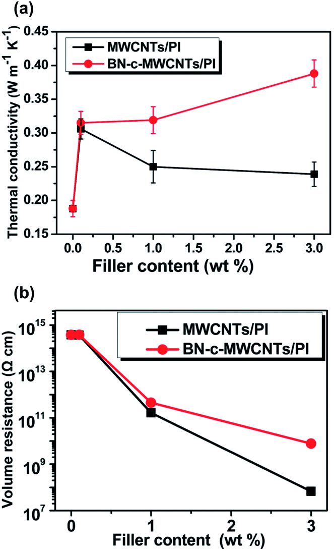 | ||
| Fig. 14 (a) Thermal conductivity and (b) volume resistivity of polyimide matrix composites with either raw MWCNT filler or h-BN coated MWCNT filler at three different weight percentages. Reproduced from ref. 34 with permission from the Royal Society of Chemistry. | ||
The MWCNT@BN fillers did enhance the thermal conductivity of the PI films for all filler contents tested (0.1%, 1%, 3%). Without any filler the PI film has κ = 0.188 W m−1. At the highest tested filler content of 3 wt%, PI + MWCNT@BN had κ of 0.388 W m−1 K−1 whilst PI + MWCNT had κ at 0.239 W m−1 K−1.
Further investigation of h-BN effects on dispersibility of MWCNT@BN in the polymer matrix and polymer-nanotube interfacial resistance can be done to optimise the performance of the composites. The h-BN coating thickness/crystallinity etc. are also variable parameters that can be studied to influence composite properties.
3.7 Field emitters
The phenomenon of field emission (FE) occurs by the extraction of electrons from a solid into vacuum as facilitated by the presence of an electric field. Sharp, conductive needle-like objects present the advantage of concentrating an electric field at their tips, thereby allowing a lower threshold voltage to onset electron emission. This field enhancement factor, β, is estimated to be proportional to the aspect ratio of the emitter. In this regard, the inherently high aspect ratio of CNTs lends to them being candidates for FE to replace the Spindt-type metal or silicon emitters.106,107 Applications for field emitters include inter alia, FE displays, X-ray sources, microwave amplifiers, vacuum electronics, E-beam lithography and high resolution electron microscopes.108CNTs, although promising as field emitters, do exhibit some shortfalls. For instance, CNT emitters have been found to exhibit emission current fluctuation, which has been attributed to the adsorption of remaining gas molecules in moderate vacuum conditions. By coating CNTs with h-BN, emission current stability has been markedly improved.27,36,40 This improvement has been credited to the chemical inertness of the h-BN, which prevents contaminant gas adsorption that can affect the emitter work function.36 In an oxygen ambient, h-BN coated CNTs also exhibited emission current degradation that was an order of magnitude smaller than that of bare CNTs.47
Advantageous lowering of the emitter turn-on applied field has also been observed on h-BN coated CNTs compared to pristine CNTs. The deposition of h-BN on CNTs is deemed to decrease the potential energy barrier for electrons to tunnel across from CNT to h-BN, from which they are then more easily ejected into vacuum due to the negative energy affinity of the h-BN surface. This effect is thickness dependent, thereby emphasizing the need for h-BN coating thickness control. Thinner h-BN coating thicknesses were found to bring about the highest reduction in turn-on field relative to the bare CNTs. Morihisa et al., (2008) found that a 3 nm h-BN coating reduced the turn-on field of CNTs by 32% whilst a 8 nm coat caused an increase of 8%.40 Yang et al., (2015) found a 67% and 31% decrease for 3 nm and 8 nm coats respectively (see Fig. 15a).36 Thicker coatings can contribute to electron inelastic scattering in the h-BN layers, resulting in energy loss and higher turn-on fields required to emit electrons to vacuum.36
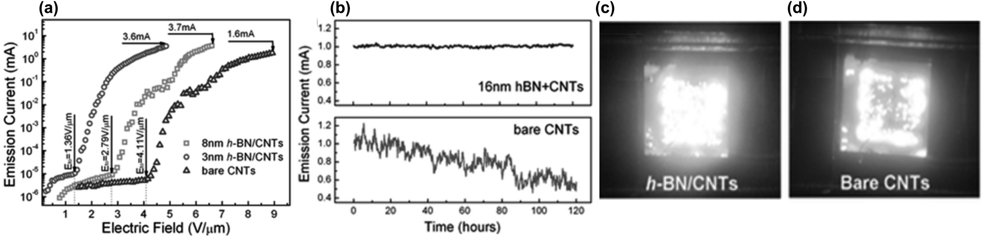 | ||
| Fig. 15 (a) Graph showing that the 3 nm h-BN coating on MWCNTs reduced the emission turn on field in comparison to pristine MWCNTs and MWCNTs coated with 8 nm BN. (b) By introducing a h-BN coating, the emission current stability was significantly enhanced in comparison to bare CNTs. (c) Emission images for 2 mm × 2 mm array of VA-MWCNTs coated with 3 nm h-BN compared to (d) pristine MWCNTs. Reproduced with permission from ref. 36. Copyright 2015, Wiley-VHC. | ||
There was also evidence which suggests that the h-BN coating crystallinity could influence the FE properties of the CNT@BN hybrid. Su et al., (2007) described that CNT@BN arrays with h-BN generated by sputter coating presented better FE properties than h-BN coatings synthesized by PACVD.41 This could be due to more crystal defects at the CNT/sputter deposited BN interface, which generate a higher internal electric field that acts to further reduce the energy barrier for electron emission. Chang et al., also partially attributed a reduced turn-on field to sharp edges created by the h-BN coat, resulting in enhanced β.27
The maximum field emission current of a CNT array was also increased after h-BN coating, as shown by Yang et al., (2015).36 This improvement was ascribed to the ability of the h-BN to dissipate heat generated during the emission, such that heat induced ‘burnout’ was averted at higher operating emission currents. Additionally, the h-BN modified arrays exhibited more emission uniformity over the same sample emission area as bare CNTs. See Fig. 15b–d.36
4 Conclusion and perspectives
Core–shell nanotubes consisting of CNTs sheathed in h-BN represent a rapidly emerging family of multi-functional heteronanotubes. In this review, we have highlighted the major advances in synthesis and characterisation of CNT@BN nanotubes, along with their properties that make them highly desirable for state-of-the-art applications in nano/microelectronics, thermal management solutions, nano-mechanical systems, field emission devices and structural composites.The progress in synthesis of CNT@BN nanotubes is presented from a comparative perspective, with focus on the efficiency and accessibility of the synthesis methods and importantly, on the quality of the CNT@BN. Our discussion on CNT@BN quality with a focus on structure, crystallinity and bond composition of the heteronanotube establishes a framework for their evaluation that we hope will promote future standardised characterisation1 of CNT@BN nanotubes.
Notably, there are challenges remaining with regard to the synthesis of CNT@BN nanotubes. Whilst there has been significant development in exploring a range of precursor pathways for CVD deposition of h-BN onto CNTs, there are relatively few studies that demonstrated an ability to control h-BN parameters such as thickness. Secondly, the multiple types of CNT material, with differing degrees of crystallinity and dimensions, introduces an uncontrolled variable across the studies. As the underlying CNT crystallinity has been demonstrated to influence the deposited h-BN crystallinity, this lateral variable adds a degree of uncertainty when determining the influence of the precursor pathway on the quality of the CVD deposited h-BN. We also observed that true van der Waals heteronanotubes composed of uniform and continuous crystals of h-BN encapsulating crystalline CNTs form only a small subset in the literature on core–shell CNT@BN hybrids. Most studies have h-BN crystallinity in the range of polycrystalline to turbostratic. Furthermore, many CNT@BN structures synthesised to date have appreciable covalent B–C and N–C bonds, especially those synthesized by the B2O3 and NH3 precursor pathway (and similar chemical variants). Heteronanotubes that have both van der Waals and covalent hybridisation of h-BN and graphitic carbon have properties that cannot be solely attributed to the presence of an outer h-BN sheath. In terms of the synthesis scalability, the CVD strategy of depositing h-BN is currently more accessible than growth of CNTs inside BNNTs by electron irradiation conversion of C60/amorphous carbon. However, several CVD methods still have a high time expenditure, particularly methods involving the use of aqueous precursors, thus making these less feasible for industry scale adaptation.
We propose here some research avenues that are necessary for developments relevant to CNT@BN synthesis:
(i) The growth mechanisms of h-BN on the CNT surface should be studied with respect to the various chemical pathways. This could help to determine the limiting factors of CVD deposited h-BN growth so that synthesis parameters such as temperature, gas flow rate, gas composition etc. are informedly tuned to control h-BN coating parameters such as morphology, thickness or crystallinity.
(ii) To address the issue of CNT variability across studies, a comparative study utilising a standard CNT template could be conducted. By testing multiple CVD precursor pathways on the same CNT template, the different effects of each pathway, if any, could become more apparent.
(iii) CVD methods that implement a single source gaseous precursors, such as ammonia borane, present advantages over several two precursor routes, including safety in storage and handling and minimum time consumption when preparing nanotubes for the growth reactor. This precursor may also be more favourable to avoid the formation of covalent bonds between the CNT and h-BN layers. Further studies are needed to explore the benefits of this novel precursor in the field of CNT@BN synthesis.
We also highlighted in this review the nascent exploration of CNT@BN applicability. Empirical measurement of CNT@BN properties and consideration of their application has garnered increased research attention within the last five years, prompted by productivity in the area of synthesis. We conclude with a few recommended research opportunities toward investigating the properties and applications of CNT@BN heteronanotubes:
(i) To date, empirical measurements of CNT@BN nanotubes (e.g. thermal and electrical conductivity, mechanical performance etc.) have been dominantly conducted on their macroscopic architectures, with a prevalence of vertically aligned assemblies. However, the properties of individual CNT@BN nanotubes have mainly been investigated in silico, leaving considerable scope for empirical investigation at the individual nanotube scale, as well as on other macroscopic structures such as aerogels and random network films or sheets.
(ii) An avenue of research yet to be empirically explored is the comparison of individual nanotube properties amongst CNT@BNs, CNTs and BNNTs. Ideally, nanotubes of similar dimensions (diameter, number of walls etc.) should be compared, which requires overcoming challenges associated with single nanotube measurement and fine control of nanotube structure during synthesis.
(iii) To the best of our knowledge, there is currently one study on a nano-composite composed of CNT@BN with polyimide polymer, and no studies have yet reported on CNT@BN composites with ceramic or metal matrices, leaving this as a field with prospects for novel investigation. This research is highly desirable to develop the urgently needed next generation of thermal management materials for the electronics industry and high temperature resistant, structurally reinforced composites demanded in e.g. the aerospace or nuclear energy industries.
(iv) There is still significant progress to be made in the applications testing of true van der Waals hybrids of CNT@BN, and to clearly distinguish their measured properties from CNT@BN grades that are partially covalent hybrids.
(v) It is essential to establish which characteristics of the CNT@BN should be prioritized for different applications. For example, for field emission applications, few h-BN layers appear to be preferential for enhancing the FE properties of the underlying CNT. There is also some indication that a high crystallinity is not required for this. For properties such as oxidation resistance, the higher the crystallinity of the h-BN, the more it is oxidatively stable. The same trend is predicted for mechanical, thermal and dielectric performance. Ensuing work could develop the CNT@BN quality criteria for various application.
(vi) We presented here a non-exhaustive list of potential applications of CNT@BN heteronanotubes, which are at the forefront of the trend towards compacting multi-functionality into nanomaterials. Future research could venture towards applying CNT@BN in flexible electronics, optoelectronics, energy conversion devices and nanoscale bearings.109
Conflicts of interest
There are no conflicts to declare.Acknowledgements
We thank the Royal Society (NG) and the EPSRC (EP/R031975/1; NG, BM) for financial support.References
- N. Grobert, Mater. Today, 2007, 10, 28–35 CrossRef CAS.
- R. Arenal, X. Blase and A. Loiseau, Adv. Phys., 2010, 59, 101–179 CrossRef CAS.
- O. Stephan, P. M. Ajayan, C. Colliex, P. Redlich, J. M. Lambert, P. Bernier and P. Lefin, Science, 1994, 266, 1683–1685 CrossRef CAS.
- M. L. Cohen and A. Zettl, Phys. Today, 2010, 63, 34–38 CrossRef CAS.
- C. Zhi, Y. Bando, C. Tang and D. Golberg, Mater. Sci. Eng., R, 2010, 70, 92–111 CrossRef.
- C. Dekker, et al. , Phys. Today, 1999, 52, 22–30 CAS.
- T. Ebbesen, H. Lezec, H. Hiura, J. Bennett, H. Ghaemi and T. Thio, Nature, 1996, 382, 54–56 CAS.
- X. Blase, J.-C. Charlier, A. De Vita and R. Car, Appl. Phys. Lett., 1997, 70, 197–199 CrossRef CAS.
- C. Y. Zhi, J. D. Guo, X. D. Bai and E. G. Wang, J. Appl. Phys., 2002, 91, 5325–5333 CrossRef CAS.
- Y. Miyamoto, A. Rubio, M. L. Cohen and S. G. Louie, Phys. Rev. B: Condens. Matter Mater. Phys., 1994, 50, 4976–4979 CrossRef CAS.
- X. Yang, L. Liu, M. Wu, W. Wang, X. Bai and E. Wang, J. Am. Chem. Soc., 2011, 133, 13216–13219 CrossRef CAS.
- K. S. Novoselov, A. Mishchenko, A. Carvalho and A. H. Castro Neto, Science, 2016, 353, 6298 CrossRef.
- K. Suenaga, C. Colliex, N. Demoncy, A. Loiseau, H. Pascard and F. Willaime, Science, 1997, 278, 653–655 CrossRef CAS.
- R. Nakanishi, R. Kitaura, J. H. Warner, Y. Yamamoto, S. Arai, Y. Miyata and H. Shinohara, Sci. Rep., 2013, 3, 1385 CrossRef.
- Y. Kuang, S. Shi, P. Chan and C. Chen, Comput. Mater. Sci., 2010, 50, 645–650 CrossRef CAS.
- A. B. Belgacem, I. Hinkov, S. B. Yahia, O. Brinza and S. Farhat, Mater. Today Commun., 2016, 8, 183–195 CrossRef.
- R. Wang and H. Zhang, New J. Phys., 2004, 6, 78 CrossRef.
- P. Kohler-Redlich, M. Terrones, C. Manteca-Diego, W. Hsu, H. Terrones, M. Rühle, H. Kroto and D. Walton, Chem. Phys. Lett., 1999, 310, 459–465 CrossRef CAS.
- S. Enouz-Védrenne, O. Stéphan, M. Glerup, J.-L. Cochon, C. Colliex and A. Loiseau, J. Phys. Chem. C, 2008, 112, 16422–16430 CrossRef.
- R. Xiang, T. Inoue, Y. Zheng, A. Kumamoto, Y. Qian, Y. Sato, M. Liu, D. Tang, D. Gokhale, J. Guo, K. Hisama, S. Yotsumoto, T. Ogamoto, H. Arai, Y. Kobayashi, H. Zhang, B. Hou, A. Anisimov, M. Maruyama, Y. Miyata, S. Okada, S. Chiashi, Y. Li, J. Kong, E. I. Kauppinen, Y. Ikuhara, K. Suenaga and S. Maruyama, Science, 2020, 367, 537–542 CrossRef CAS.
- L. Jing, R. Y. Tay, H. Li, S. H. Tsang, J. Huang, D. Tan, B. Zhang, E. H. T. Teo and A. I. Y. Tok, Nanoscale, 2016, 8, 11114–11122 RSC.
- L. Jing, M. K. Samani, B. Liu, H. Li, R. Y. Tay, S. H. Tsang, O. Cometto, A. Nylander, J. Liu, E. H. T. Teo and A. I. Y. Tok, ACS Appl. Mater. Interfaces, 2017, 9, 14555–14560 CrossRef CAS.
- P. Wang, Y. Zheng, T. Inoue, R. Xiang, A. Shawky, M. Watanabe, A. Anisimov, E. I. Kauppinen, S. Chiashi and S. Maruyama, ACS Nano, 2020, 14(4), 4298–4305 CrossRef CAS.
- W. Mickelson, S. Aloni, W.-Q. Han, J. Cumings and A. Zettl, Science, 2003, 300, 467–469 CAS.
- K. E. Walker, G. A. Rance, Á. Pekker, H. M. Tóháti, M. W. Fay, R. W. Lodge, C. T. Stoppiello, K. Kamarás and A. N. Khlobystov, Small Methods, 2017, 1, 1700184 Search PubMed.
- R. Arenal and A. Lopez-Bezanilla, ACS Nano, 2014, 8, 8419–8425 CrossRef CAS.
- H.-C. Chang, H.-J. Tsai, W.-Y. Lin, Y.-C. Chu and W.-K. Hsu, ACS Appl. Mater. Interfaces, 2015, 7, 14456–14462 CrossRef CAS.
- W.-H. Chiang, C.-Y. Hsieh, S.-C. Lo, Y.-C. Chang, T. Kawai and Y. Nonoguchi, Carbon, 2016, 109, 49–56 CrossRef CAS.
- L. Chen, H. Ye and Y. Gogotsi, J. Am. Ceram. Soc., 2004, 87, 147–151 CrossRef CAS.
- I. Mohai, M. Mohai, I. Bertóti, Z. Sebestyén, P. Németh, I. Z. Babievskaya and J. Szépvölgyi, Diamond Relat. Mater., 2011, 20, 227–231 CrossRef CAS.
- R. Y. Tay, H. Li, S. H. Tsang, L. Jing, D. Tan, M. Wei and E. H. T. Teo, Chem. Mater., 2015, 27, 7156–7163 CrossRef CAS.
- Y. Joo Jeong and M. F. Islam, Nanoscale, 2015, 7, 12888–12894 CAS.
- A. Gomathi, M. R. Harika and C. Rao, Mater. Sci. Eng., A, 2008, 476, 29–33 Search PubMed.
- W. Yan, Y. Zhang, H. Sun, S. Liu, Z. Chi, X. Chen and J. Xu, J. Mater. Chem. A, 2014, 2, 20958–20965 CAS.
- X. Li, Q. Li and G.-X. Chen, Mater. Lett., 2014, 134, 38–41 CrossRef CAS.
- X. Yang, Z. Li, F. He, M. Liu, B. Bai, W. Liu, X. Qiu, H. Zhou, C. Li and Q. Dai, Small, 2015, 11, 3710–3716 CrossRef CAS.
- Q. M. Zou, L. M. Deng, P. X. Fan, D. W. Li, C. F. Zhang, L. S. Fan, L. Jiang, J.-F. Silvain and Y. F. Lu, ACS Appl. Nano Mater., 2019, 2, 100–108 CrossRef CAS.
- Y. Song, B. Li, S. Yang, G. Ding, C. Zhang and X. Xie, Sci. Rep., 2015, 5, 10337 CrossRef CAS.
- W.-L. Wang, J.-Q. Bi, W.-X. Sun, H.-L. Zhu, J.-J. Xu, M.-T. Zhao and Y.-J. Bai, Mater. Chem. Phys., 2010, 122, 129–132 CrossRef CAS.
- Y. Morihisa, C. Kimura, M. Yukawa, H. Aoki, T. Kobayashi, S. Hayashi, S. Akita, Y. Nakayama and T. Sugino, J. Vac. Sci. Technol., B: Microelectron. Nanometer Struct.--Process., Meas., Phenom., 2008, 26, 872–875 CrossRef CAS.
- C. Su, Z. Juang, Y. Chen, K. Leou and C. Tsai, Diamond Relat. Mater., 2007, 16, 1393–1397 CrossRef CAS.
- J. Cumings and A. Zettl, Chem. Phys. Lett., 2000, 316, 211–216 CrossRef CAS.
- R. Arenal, O. Stephan, J.-L. Cochon and A. Loiseau, J. Am. Chem. Soc., 2007, 129, 16183–16189 CrossRef CAS.
- M. W. Smith, K. C. Jordan, C. Park, J.-W. Kim, P. T. Lillehei, R. Crooks and J. S. Harrison, Nanotechnology, 2009, 20, 505604 CrossRef.
- A. Lipp, K. Schwetz and K. Hunold, J. Eur. Ceram. Soc., 1989, 5, 3–9 CrossRef CAS.
- V. Babenko, G. Lane, A. A. Koos, A. T. Murdock, K. So, J. Britton, S. S. Meysami, J. Moffat and N. Grobert, Sci. Rep., 2017, 7, 1–12 CrossRef.
- J. Yoo, J. Han, S. Choi, T. Lee, C. Park, T. Jeong, J. Lee, S. Yu, G. Park, W. Yi, H. Kim, Y.-J. Baik and J. Kim, Phys. B, 2002, 323, 180–181 CrossRef CAS.
- M. Mohai and I. Bertóti, Surf. Interface Anal., 2004, 36, 805–808 CrossRef CAS.
- M. Mohai, I. Mohai, Z. Sebestyén, A. Gergely, P. Németh and J. Szépvölgyi, Surf. Interface Anal., 2010, 42, 1148–1151 CrossRef CAS.
- Y. Li, M. Yang, B. Xu, Q. Sun, W. Zhang, Y. Zhang and F. Meng, Appl. Surf. Sci., 2018, 450, 284–291 CrossRef CAS.
- J.-S. Li, C.-R. Zhang and B. Li, Appl. Surf. Sci., 2011, 257, 7752–7757 CrossRef CAS.
- C. G. Cofer and J. Economy, Carbon, 1995, 33, 389–395 CrossRef CAS.
- M. T. Alam, M. S. Bresnehan, J. A. Robinson and M. A. Haque, Appl. Phys. Lett., 2014, 104, 013113 CrossRef.
- X. Wei, M.-S. Wang, Y. Bando and D. Golberg, Adv. Mater., 2010, 22, 4895–4899 CrossRef CAS.
- J. Thomas, N. E. Weston and T. E. O'Connor, J. Am. Chem. Soc., 1962, 84, 4619–4622 CrossRef CAS.
- M. Pimenta, G. Dresselhaus, M. S. Dresselhaus, L. Cancado, A. Jorio and R. Saito, Phys. Chem. Chem. Phys., 2007, 9, 1276–1290 RSC.
- R. Geick, C. Perry and G. Rupprecht, Phys. Rev., 1966, 146, 543 CrossRef CAS.
- R. Nemanich, S. Solin and R. M. Martin, Phys. Rev. B: Condens. Matter Mater. Phys., 1981, 23, 6348 CrossRef CAS.
- N. Mishra, V. Miseikis, D. Convertino, M. Gemmi, V. Piazza and C. Coletti, Carbon, 2016, 96, 497–502 CrossRef CAS.
- L. Liu, J. Park, D. A. Siegel, K. F. McCarty, K. W. Clark, W. Deng, L. Basile, J. C. Idrobo, A.-P. Li and G. Gu, Science, 2014, 343, 163–167 CrossRef CAS.
- P. Van der Heide, X-ray photoelectron spectroscopy: an introduction to principles and practices, Wiley, Hoboken, N.J., 2012 Search PubMed.
- S. Y. Kim, J. Park, H. C. Choi, J. P. Ahn, J. Q. Hou and H. S. Kang, J. Am. Chem. Soc., 2007, 129, 1705–1716 CrossRef CAS.
- R. Blume, D. Rosenthal, J.-P. Tessonnier, H. Li, A. Knop-Gericke and R. Schlögl, ChemCatChem, 2015, 7, 2871–2881 CrossRef CAS.
- N. Grobert, M. Terrones, S. Trasobares, K. Kordatos, H. Terrones, J. Olivares, J. Zhang, P. Redlich, W. Hsu and C. Reeves, et al. , Appl. Phys. A: Mater. Sci. Process., 2000, 70, 175–183 CrossRef CAS.
- J. H. Kim, T. V. Pham, J. H. Hwang, C. S. Kim and M. J. Kim, Nano Convergence, 2018, 5, 1–13 CrossRef CAS.
- K. S. Kim, M. J. Kim, C. Park, C. C. Fay, S.-H. Chu, C. T. Kingston and B. Simard, Semicond. Sci. Technol., 2016, 32, 013003 CrossRef.
- J. Wang, C. H. Lee and Y. K. Yap, Nanoscale, 2010, 2, 2028–2034 RSC.
- H. Li, R. Y. Tay, S. H. Tsang, L. Jing, M. Zhu, F. N. Leong and E. H. T. Teo, RSC Adv., 2017, 7, 12511–12517 RSC.
- W.-Q. Han, J. Cumings, X. Huang, K. Bradley and A. Zettl, Chem. Phys. Lett., 2001, 346, 368–372 CrossRef CAS.
- F. Deepak, C. Vinod, K. Mukhopadhyay, A. Govindaraj and C. Rao, Chem. Phys. Lett., 2002, 353, 345–352 CrossRef CAS.
- T. Yamamoto, K. Watanabe and E. R. Hernández, in Mechanical Properties, Thermal Stability and Heat Transport in Carbon Nanotubes, ed. A. Jorio, G. Dresselhaus and M. S. Dresselhaus, Springer Berlin Heidelberg, Berlin, Heidelberg, 2008, pp. 165–195 Search PubMed.
- W. A. Curtin and B. W. Sheldon, Mater. Today, 2004, 7, 44–49 CrossRef CAS.
- J. H. Lehman, M. Terrones, E. Mansfield, K. E. Hurst and V. Meunier, Carbon, 2011, 49, 2581–2602 CrossRef CAS.
- W. Huang, Y. Wang, G. Luo and F. Wei, Carbon, 2003, 41, 2585–2590 CrossRef CAS.
- E. Kowalska, P. Kowalczyk, J. Radomska, E. Czerwosz, H. Wronka and M. Bystrzejewski, J. Therm. Anal. Calorim., 2006, 86, 115–119 CrossRef CAS.
- S. Osswald, M. Havel and Y. Gogotsi, J. Raman Spectrosc., 2007, 38, 728–736 CrossRef CAS.
- A. Agarwal, S. R. Bakshi and D. Lahiri, Carbon nanotubes: reinforced metal matrix composites, CRC Press, 2018 Search PubMed.
- Z. Liu, Y. Gong, W. Zhou, L. Ma, J. Yu, J. C. Idrobo, J. Jung, A. H. MacDonald, R. Vajtai and J. Lou, et al. , Nat. Commun., 2013, 4, 1–8 CAS.
- D. Golberg, Y. Bando, K. Kurashima and T. Sato, Scr. Mater., 2001, 44, 1561–1565 CrossRef CAS.
- Y. Chen, J. Zou, S. J. Campbell and G. Le Caer, Appl. Phys. Lett., 2004, 84, 2430–2432 CrossRef CAS.
- X. Chen, C. M. Dmuchowski, C. Park, C. C. Fay and C. Ke, Sci. Rep., 2017, 7, 1–9 CrossRef.
- M. Das, A. Basu, S. Ghatak and A. G. Joshi, J. Eur. Ceram. Soc., 2009, 29, 2129–2134 CrossRef CAS.
- A. A. El-Barbary, R. H. Telling, C. P. Ewels, M. I. Heggie and P. R. Briddon, Phys. Rev. B: Condens. Matter Mater. Phys., 2003, 68, 144107 CrossRef.
- W.-L. Wang, J.-Q. Bi, K.-N. Sun, M. Du, N.-N. Long and Y.-J. Bai, J. Am. Ceram. Soc., 2011, 94, 3636–3640 CrossRef CAS.
- D. Lahiri, A. Hadjikhani, C. Zhang, T. Xing, L. H. Li, Y. Chen and A. Agarwal, Mater. Sci. Eng., A, 2013, 574, 149–156 CrossRef CAS.
- M. M. H. Bhuiyan, J. Wang, L. H. Li, P. Hodgson, A. Agarwal, M. Qian and Y. Chen, J. Mater. Res., 2017, 32, 3744–3752 CrossRef CAS.
- C. Daraio, V. F. Nesterenko and S. Jin, Appl. Phys. Lett., 2004, 85, 5724–5726 CrossRef CAS.
- J. Suhr, P. Victor, L. Ci, S. Sreekala, X. Zhang, O. Nalamasu and P. Ajayan, Nat. Nanotechnol., 2007, 2, 417–421 CrossRef CAS.
- A. Cao, P. L. Dickrell, W. G. Sawyer, M. N. Ghasemi-Nejhad and P. M. Ajayan, Science, 2005, 310, 1307–1310 CrossRef CAS.
- H. Badjian and A. Setoodeh, Phys. B, 2017, 507, 156–163 CrossRef CAS.
- K. M. Liew and J. Yuan, Nanotechnology, 2011, 22, 085701 CrossRef CAS.
- J. Yuan and K. M. Liew, Carbon, 2011, 49, 677–683 CrossRef CAS.
- T. He, T. Li, Z. Huang, Z. Tang and X. Guan, Phys. E, 2019, 107, 182–186 CrossRef CAS.
- A. N. Enyashin, G. Seifert and A. L. Ivanovskii, J. Exp. Theor. Phys. Lett., 2004, 80, 608–611 CrossRef CAS.
- A. N. Enyashin and A. L. Ivanovskii, Nanotechnology, 2005, 16, 1304–1310 CrossRef CAS.
- Z. Zhang, W. Guo and G. Tai, Appl. Phys. Lett., 2007, 90, 133103 CrossRef.
- J.-H. Ting, C.-C. Chiu and F.-Y. Huang, J. Vac. Sci. Technol., B: Microelectron. Nanometer Struct.--Process., Meas., Phenom., 2009, 27, 1086–1092 CAS.
- A. L. Moore and L. Shi, Mater. Today, 2014, 17, 163–174 CrossRef CAS.
- J. Hansson, T. M. J. Nilsson, L. Ye and J. Liu, Int. Mater. Rev., 2018, 63, 22–45 CAS.
- J. Xu and T. S. Fisher, IEEE Trans. Compon. Packag. Technol., 2006, 29, 261–267 CAS.
- P. Kim, L. Shi, A. Majumdar and P. L. McEuen, Phys. Rev. Lett., 2001, 87, 215502 CrossRef CAS.
- E. Pop, D. Mann, Q. Wang, K. Goodson and H. Dai, Nano Lett., 2006, 6, 96–100 CrossRef CAS.
- B. Kumanek and D. Janas, J. Mater. Sci., 2019, 54, 7397–7427 CrossRef CAS.
- C. W. Chang, A. M. Fennimore, A. Afanasiev, D. Okawa, T. Ikuno, H. Garcia, D. Li, A. Majumdar and A. Zettl, Phys. Rev. Lett., 2006, 97, 085901 CrossRef CAS.
- D. Frear, in Packaging Materials, ed. S. Kasap and P. Capper, Springer International Publishing, Cham, 2017, p. 1 Search PubMed.
- O. Gröning, R. Clergereaux, L.-O. Nilsson, P. Ruffieux, P. Gröning and L. Schlapbach, CHIMIA International Journal for Chemistry, 2002, 56, 553–561 CrossRef.
- Y. Cheng and O. Zhou, C. R. Phys., 2003, 4, 1021–1033 CrossRef CAS.
- W. Milne, K. Teo, G. Amaratunga, P. Legagneux, L. Gangloff, J.-P. Schnell, V. Semet, V. T. Binh and O. Groening, J. Mater. Chem., 2004, 14, 933–943 CAS.
- Y. Gogotsi and B. I. Yakobson, Science, 2020, 367, 506–507 CAS.
| This journal is © The Royal Society of Chemistry 2020 |