
 Open Access Article
 This Open Access Article is licensed under a Creative Commons Attribution-Non Commercial 3.0 Unported Licence
Effects of gas-phase and wet-chemical surface treatments on substrates induced vertical, valley–hill & micro-granular growth morphologies of close space sublimated CdTe films†
Kulandai Velu
Ramanathan
a,
Balakrishnan
Shankar
b,
Shantikumar V.
Nair
a and
Mariyappan
Shanmugam
 *a
*a
aAmrita Centre for Nanosciences and Molecular Medicine, Amrita Vishwa Vidyapeetham, Kochi, Kerala – 682041, India. E-mail: mshanmugham@aims.amrita.edu
bDepartment of Mechanical Engineering, Amrita Vishwa Vidyapeetham, Amritapuri, Kerala – 690525, India
First published on 17th August 2020
Abstract
We implemented gas-phase (argon plasma) and wet-chemical (HNO3) surface treatments on close space sublimated (CSS) Cadmium Telluride (CdTe) thin films exhibiting morphologies of (i) vertically aligned walls on copper (Cu) and stainless steel (SS) substrates, (ii) valley–hills on aluminum (Al) substrates and (iii) micro-granules on nickel (Ni). As all the growth conditions (temperature, pressure, duration and source/substrate distance) were exactly the same in the CSS process to coat CdTe films, it is asserted that the various microstructures were raised only on Cu, Al, Ni and SS substrates. Plasma and HNO3 surface treatments on metal substrates did not affect the CdTe morphologies in terms of specific structures but it was observed that structural, optical and electrical charge transport characteristics were highly tunable by the two surface treatments. Thus, substrate driven morphological evaluation followed by surface treatments was enabled. The present study demonstrated various microstructures of CdTe films on metallic thin foil substrates to attempt the establishment of flexible opto-electronics based on CdTe.
Introduction
Light–matter interaction is the primary phenomenon which constitutes absorption, reflection, transmittance and scattering in semiconductors.1,2 Mostly, nano-structural (zero, one, two and three dimensional such as quantum dots, nanofibers/rods/tubes, exfoliated individual atomically thin planes and bulk crystals) and optical (band gap and absorption coefficient) characteristics of semiconductors determine the efficiency of light–matter interactions.3–5 Thus, it is evident that nano/micro-structures actively participate in light–matter interactions to determine essential factors which govern the primary opto-electronic characteristics of resulting semiconductor materials. While it has been identified that nano/micro-structures of thin films or the bulk of semiconductors can evidently alter light–matter interactions, the surface is also an essential factor at which the energy interaction begins.6–10 The surface of thin films or bulk semiconductors becomes a dominant factor in the case of photon management as can be evidenced from various texture formations on the surface to minimize reflection loss.11–15 Textured semiconductor surfaces have been demonstrated to achieve minimum possible optical loss and increased optical path length which facilitated efficient exciton generation. Thus, surface morphology has been realized to be a dominant governing factor through which optical characteristics of semiconductors can effectively be engineered.16,17The surface morphology of bulk and thin film semiconductors can be tailored by many different routes to achieve the desired optical features.18,19 Plasma and wet-chemical environments have been envisaged to tailor structural, optical and electrical characteristics of semiconductors.20–23 Plasma and wet-chemical treatments on thin film and bulk semiconductors can effectively enable doping, etching, polishing and surface modification which are all very interesting parameters for energy conversion technologies such as photovoltaics.24,25 Additionally, surface treatments on semiconductors are essential routes through which all sort of disorders, in general defects, can be controlled.26,27
Cadmium Telluride (CdTe) has been studied intensively for various applications including photovoltaics,28–30 nuclear radiation sensors,31 photodetectors,32–34 and medical imaging devices.35 The structural, optical and electrical characteristics of CdTe are highly favourable for light–matter interaction and thus it is one of the highly appreciated functional materials in energy conversion science and technology.36–38 Specifically, the optical bandgap of CdTe (1.5 eV)39 is an exceptional parameter which deserves special attention for the requirements of the Shockley–Queisser detailed balance limit.40 CdTe has promising applications in thin film solar cells competing with silicon, gallium arsenide and copper indium diselenide due to its optimum direct bandgap to cover the visible solar spectrum with an exceptionally high absorption coefficient.41,42 Thus, it has been predicted and demonstrated that a nearly 2 μm CdTe film is sufficient to absorb incident photons completely.43 Thin film CdTe has been processed by several methods including close space sublimation (CSS),44 RF-sputtering,45 electron beam evaporation46 and wet-chemical methods.47
While CdTe has successfully shown its record benchmark efficiency in various applications including photovoltaics, surface/interface defects are considered to be dominant factors which eventually limit the performance in terms of light–matter interaction, charge transport kinetics, carrier lifetime and overall efficiency of the resulting applications.48–50 Thus, it is an essential requirement to achieve efficient surface passivation schemes which can effectively alter and control the role of surface/interface defects on the functionality of CdTe films. In general, wet-chemical surface treatment has widely been established to enhance the quality of CdTe in terms of crystallinity, conductivity, minimized grain boundaries, and maximized grains which are all essential factors to determine the overall performance of the resulting applications.51,52 Surface treatment methodologies are direct routes to suppressing the active defects which efficiently participate in the charge transport in CdTe and play detrimental role as evidenced from previous studies.53,54 Specifically, density and activity (trapping, de-trapping and scattering) of surface and interface defects in CdTe, when it reaches the nanoscale regime, become important factors which govern light–matter interactions and follow various physical processes. However, it is favourable to implement nanostructures of CdTe in all sorts of functional applications as they show promising structural advantages in the resulting products. Thus, surface treatment methods are highly justified in the case of nanostructured CdTe to engineer the surface/interface defects.
The present work adequately addresses the possibility of obtaining three different microstructures on flexible metallic foil substrates followed by two surface treatments to engineer the morphology and charge transport kinetics. In short, we report (i) vertically aligned walls, (ii) valley–hills and (iii) micro-granules on Cu/SS, Al and Ni substrates, respectively. Further, the substrate induced CdTe microstructures were subjected to gas-phase (Ar plasma) and wet-chemical (HNO3) surface treatments to examine their roles in structural, optical and charge transport characteristics.
Experimental section
We performed CdTe film growth on Cu, Al, Ni and SS metal foils. All the four categories of metal foil were divided into three sets. The first set of all four metal foils was subjected to ultrasonic cleaning with deionized water, isopropyl alcohol and acetone as a standard cleaning procedure. The second set of four metal foils was subjected to a treatment with 1![[thin space (1/6-em)]](https://www.rsc.org/images/entities/char_2009.gif) :2 ratio solutions of HNO3 and DI water prepared in a bath. The four metal foils were immersed in the bath for 1 minute and dried at 70 °C and then rinsed with DI water. The third set of metal foils was exposed to RF-plasma generated by 50 sccm of argon gas with 150 W RF-power. The plasma exposure was performed for 30 minutes. All three sets of samples were loaded into a high vacuum CSS chamber for CdTe film deposition. We used 99.99% pure CdTe source powder, obtained from Alfa Aesar, filled evenly in a graphite crucible. The CdTe film was coated at a base pressure of 1 × 10⁻⁶ mbar with a growth temperature maintained at 555 °C (TG) and substrate temperature of 330 °C (TS). The duration of CdTe film growth was maintained (20 minutes) for all substrates to obtain uniformity in terms of thickness. Table 1 lists material and CSS process related details in brief. Fig. 1 shows digital photographic images of (a) rolled Al foil before and after coating the CdTe film. In order to test the uniformity and continuity of the CdTe film on a larger area, we coated the CdTe film on 8 cm2 Al foil as shown in Fig. 1(b). Similar attempts were made on Cu foil as shown in Fig. 1(c) and (d) showing CdTe films coated on rolled and large area Cu foil, respectively. The top and bottom images in (e) show Ni foil before and after CdTe coating, respectively. The top and bottom images in (f) show SS foil before and after CdTe coating, respectively.
:2 ratio solutions of HNO3 and DI water prepared in a bath. The four metal foils were immersed in the bath for 1 minute and dried at 70 °C and then rinsed with DI water. The third set of metal foils was exposed to RF-plasma generated by 50 sccm of argon gas with 150 W RF-power. The plasma exposure was performed for 30 minutes. All three sets of samples were loaded into a high vacuum CSS chamber for CdTe film deposition. We used 99.99% pure CdTe source powder, obtained from Alfa Aesar, filled evenly in a graphite crucible. The CdTe film was coated at a base pressure of 1 × 10⁻⁶ mbar with a growth temperature maintained at 555 °C (TG) and substrate temperature of 330 °C (TS). The duration of CdTe film growth was maintained (20 minutes) for all substrates to obtain uniformity in terms of thickness. Table 1 lists material and CSS process related details in brief. Fig. 1 shows digital photographic images of (a) rolled Al foil before and after coating the CdTe film. In order to test the uniformity and continuity of the CdTe film on a larger area, we coated the CdTe film on 8 cm2 Al foil as shown in Fig. 1(b). Similar attempts were made on Cu foil as shown in Fig. 1(c) and (d) showing CdTe films coated on rolled and large area Cu foil, respectively. The top and bottom images in (e) show Ni foil before and after CdTe coating, respectively. The top and bottom images in (f) show SS foil before and after CdTe coating, respectively.
| Substrates | Purity/grade | Thickness | Manufacturer | CdTe TG/TS (°C) |
|---|---|---|---|---|
| Cu | 99.99% | 024 μm | MTI Corp. | 555/330 |
| Al | 99.30% | 015 μm | MTI Corp. | 555/330 |
| Ni | 99.00% | 500 μm | — | 555/330 |
| SS | SS 316 | 100 μm | MTI Corp. | 555/330 |
 | ||
| Fig. 1 Digital images of CdTe films coated on (a) rolled and (b) large area Al foil. (c) and (d) CdTe films coated on rolled and large area Cu foil, respectively. Top and bottom images in (e) show Ni foil before and after CdTe coating, respectively. Top and bottom images in (f) show SS foil before and after CdTe coating, respectively. | ||
The CSS processed CdTe films on four substrates with two surface treatments were subjected to field emission scanning electron microscopy (FESEM) studies to examine the surface morphology using a JSN 7610S Plus JEOL-JSM-6490-LA scanning electron microscope. X-ray diffraction (XRD) measurements were performed on all CdTe samples using a PANalytical X'Pert PRO X-ray diffractometer. Further, the values of the average crystallite sizes of CdTe samples were calculated using the Debye–Scherrer equation. UV-visible optical absorption measurements were performed on CdTe samples using a PerkinElmer Lambda-750 spectrophotometer. In order to evaluate charge transport kinetics in CdTe to assess the effect of morphology and surface treatments, we fabricated two terminal device configurations using carbon as ohmic contacts with a spacing of 0.5 mm. The current–voltage (I–V) characteristics of CdTe films were measured under dark and illuminated conditions in a Probe Station equipped with a Keithley 2420 source meter in an applied bias region of −5 V to 5 V.
Results and discussion
The three SEM images shown in column 1 of Fig. 2 show low-magnification surface morphologies of the pristine, HNO3 and plasma treated Cu foil used for CdTe coating in the CSS process. The three SEM images shown in column 2 are the surface morphologies of CdTe films coated on pristine, HNO3 and plasma treated Cu foil using the CSS process. All the three CdTe surface morphologies were acquired at a magnification of 1000×. Column 3 in Fig. 2 shows higher magnification (20000×) SEM images of column 2 to show the microstructures of CdTe films clearly. The very first observation was that CSS yielded crack-free and continuous CdTe growth on all three Cu substrates. CdTe growth on pristine Cu foil was found to be vertically oriented micron-size platelets distributed randomly as can be evidenced from column 2 in Fig. 2. At a magnification of 20000×, it can be evidenced that the CSS process yielded flat-terminated vertically oriented platelets. This means that the platelets were well-faceted and did not show any sharply terminated edges as can be realized from the SEM images listed in column 3. In Fig. 2, row 2 shows the microstructures of the CdTe film grown on Cu foil which was treated with HNO3 as detailed in the Experimental section. The first SEM image in row 2 represent the surface morphology of the HNO3 treated Cu foil and the other two show the surface morphologies of CdTe films at 5000× and 20000× on HNO3 treated Cu foil. As we did not make any other changes in the CSS process, such as pressure and temperature, except the HNO3 treatment on Cu foil, it is direct evidence that the morphology change occurred due to the surface treatment. Compared with the SEM images in row 1, the microstructures shown in row 2 demonstrated less-densely distributed CdTe. Further, it is important to observe that the edges of the CdTe platelets were sharpened very well and the entire microstructure shown in row 1 was evidently transformed into vertically aligned wall-like shapes. This change is attributed to HNO3 treatment on Cu foil which essentially changed the surface energy that could lead to the growth of CdTe in a very different manner in comparison with CdTe growth that occurred on pristine Cu foil.
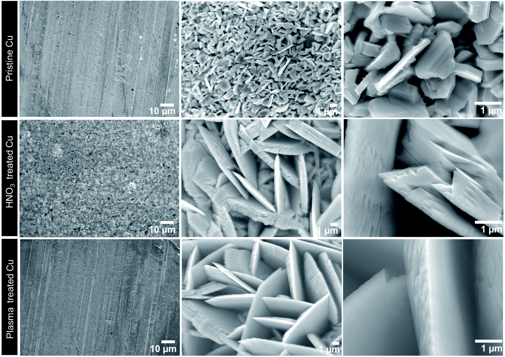 | ||
| Fig. 2 Microstructural evolution of CdTe films on pristine, HNO3 and plasma treated Cu foil. Column 1 represents the morphology of Cu foil before CdTe coating. | ||
Similar to the effect of HNO3 treatment on Cu foil, the present study also evaluated CdTe growth on Cu foil treated with Ar plasma as explained in the Experimental section. As shown in row 3, the CdTe microstructures observed at 5000× and 20000× magnifications show significant changes in morphology in comparison with CdTe grown on pristine Cu foil but very similar to the CdTe on HNO3 treated Cu foil. Thus, it can be concluded that surface treatment in terms of both wet-chemical and gas phase effectively alters the surface-chemical nature of Cu foil as a substrate. The change in the surface-chemical nature established by both HNO3 and plasma treatment is attributed to the change in morphology from platelets to vertically oriented wall-like structures with sharp edges.
The microstructures of CdTe films grown on Al foil are shown in Fig. 3. The three SEM images in column 1 of Fig. 3 show the low-magnification surface morphologies of the pristine, HNO3 and plasma treated Al foil. The three SEM images in column 2 show the surface morphologies of CdTe films coated on pristine, HNO3 and plasma treated Al foil. All the three CdTe surface morphologies, shown in column 2, were acquired at a magnification of 5000×. Column 3 in Fig. 3 shows the higher magnification (20000×) SEM images of column 2. The CdTe growth on pristine Al foil resulted in valley–hill structures of different sizes. This feature was observed only on pristine Al foil which was further treated with HNO3 and Ar plasma. The corresponding microstructures are shown in rows 2 and 3 in Fig. 3. It is evident from the SEM images shown in rows 2 and 3 that the valley–hill type of microstructures were collated into uniformly distributed CdTe clusters. It is clear that HNO3 and plasma act on the CdTe valley–hills which were eventually engineered as micro-clusters. It was also observed that the wet-chemical and gas-phase surface treatments can re-orient and re-distribute the growth morphologies to a great extent as evidenced from the morphologies shown in the three rows corresponding to pristine, HNO3 and plasma treated Al foil. It is further envisaged that HNO3 and plasma treatments on Al foil altered the surface energy distribution which limits the valley–hill type of growth and facilitated the formation of micro clusters. In other words, it is possible to attribute the formation of clusters on surface treated Al foil to the limitation of increasing selective area preferred growth as it leads to the formation of valleys and hills consecutively. As the growth of hills was suppressed and valleys were filled due to the HNO3 and plasma treatments on Al foil, it is possible to obtain uniform distribution of micro-clustered CdTe as shown in the microstructures in rows 2 and 3. In comparison with HNO3 and Ar plasma treatment, it is rather difficult to identify the changes in microstructures as they were very similar. However, it was observed that plasma treatment damaged the micro-clusters in terms of size and distribution as can be visualized in the 20000× magnified image shown in column 3. This could be due to the high energy interaction of Ar ions on the surface of Al foil which yielded different surface environment for the growth of CdTe in the CSS process. Overall, the microstructures on Al foil were significantly different from those on Cu foil as can be compared with Fig. 2.
 | ||
| Fig. 3 Microstructural evolution of CdTe films on pristine, HNO3 and plasma treated Al foil. Column 1 represents the morphology of Al foil before CdTe coating. | ||
Column 1 of Fig. 4 shows the low-magnification surface morphologies of the pristine, HNO3 and plasma treated Ni foil used for CdTe coating. The three SEM images in column 2 show the surface morphologies of CdTe films coated on pristine, HNO3 and plasma treated Ni foil. All the three CdTe surface morphologies were acquired at a magnification of 5000×. Column 3 in Fig. 4 shows the higher magnification (20000×) SEM images of column 2 to show the microstructural evolution of the CdTe films clearly.
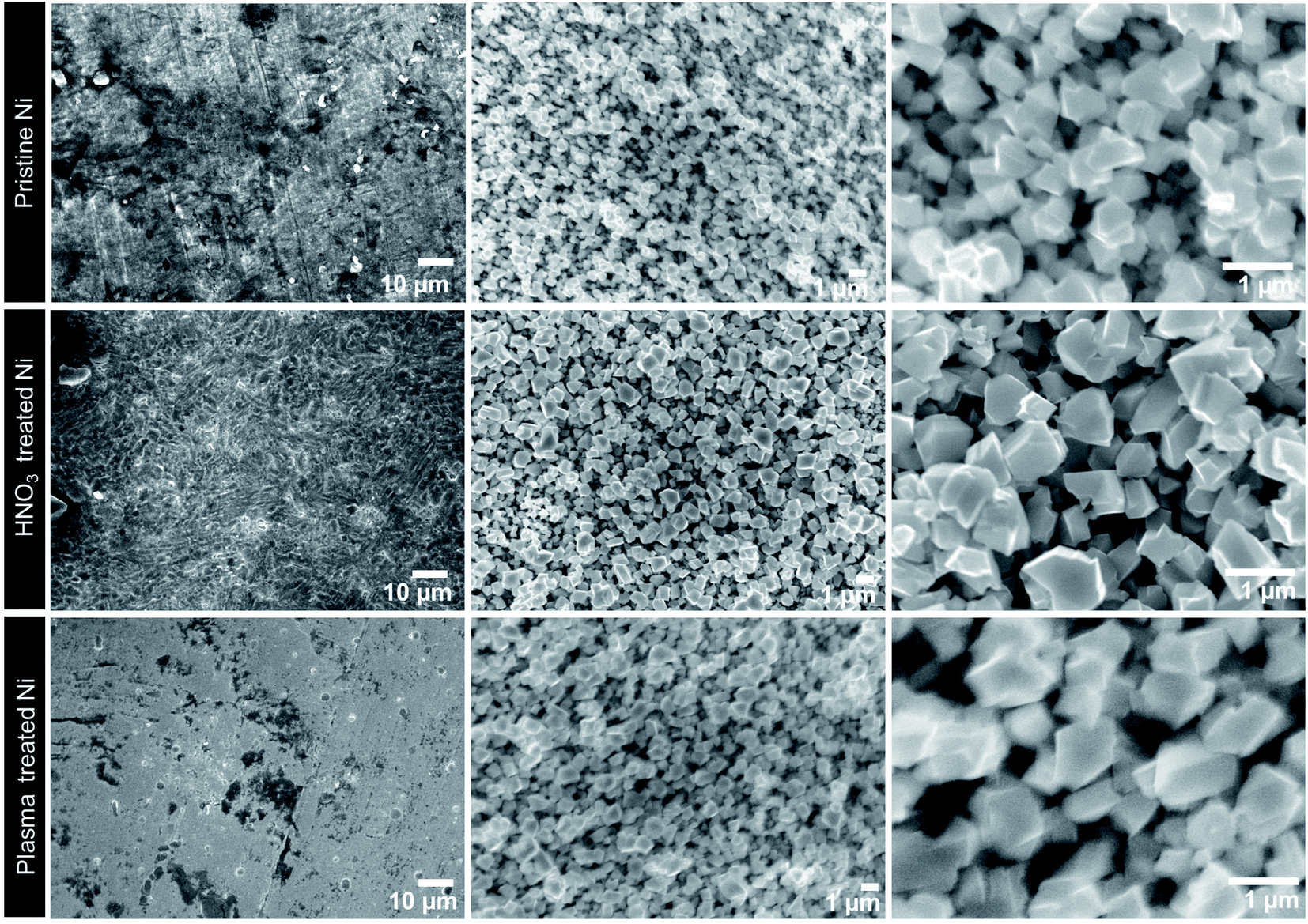 | ||
| Fig. 4 Microstructural evolution of CdTe films on pristine, HNO3 and plasma treated Cu foil. Column 1 represents the morphology of Ni foil before CdTe coating. | ||
It was observed that loosely packed micro-granular CdTe particles were randomly distributed on Ni foil. The first, second and third rows in Fig. 4 represent CdTe on pristine, HNO3 and plasma treated Ni foil, respectively. Compared with CdTe on Cu and Al foil, it is evident that Ni yielded entirely different microstructures which can be considered loosely packed micro-granular particles. It is also possible to define the CdTe film as porous as we can see the voids among the distributed CdTe particles. Row 2 in Fig. 4 shows the variation of CdTe micro-granules due to the HNO3 treatment. It is visualized that the granules were well isolated due to the HNO3 treatment in comparison with CdTe granules on pristine Ni foil. The wet-chemical treatment diffused into the microstructural voids of the film and edged the granules which resulted in granules with well-defined facets. Ar plasma treatment was observed to yield a granular structure with little increase in size as can be roughly estimated from the higher magnification SEM image shown in row 3.
The three SEM images in column 1 of Fig. 5 show the low-magnification surface morphologies of the pristine, HNO3 and plasma treated SS foil. The three SEM images in column 2 show the surface morphologies of CdTe films coated on pristine, HNO3 and plasma treated SS foil. All the three CdTe surface morphologies were acquired at a magnification of 5000×. Column 3 in Fig. 5 shows higher magnification (20000×) SEM images of column 2 to show the microstructures of CdTe films on SS foil clearly.
 | ||
| Fig. 5 Microstructural evolution of CdTe films on pristine, HNO3 and plasma treated SS foil. Column 1 shows the morphology of SS foil before CdTe coating. | ||
Row 1 in Fig. 5 shows vertically oriented CdTe micro-structures on pristine SS foil. In the case of SS, unlike Ni, the vertically grown CdTe was observed to be densely packed as can be visualised at three different magnifications. It is important to observe that HNO3 treatment on SS foil completely ruined the formation of microstructures as shown in the SEM images in row 2. In contrast, Ar plasma treatment on SS foil established the vertically aligned CdTe microstructures as presented in row 3.
The XRD pattern of CdTe on pristine Cu foil shown in Fig. 6(a) shows the polycrystalline nature of CdTe grown along the crystal orientation of Cu foil which can be seen in the XRD pattern with the high intensity peak of CdTe (111) at 24.685°, as reported elsewhere,55,56 along with Cu's high intensity peak (111) at 43.165°, with the other significant peak of CdTe (311) at 45.205° along with Cu (200) and Cu (220) at 50.515° and 74.425°, respectively. These values are in good agreement with previous studies.31,33 However , when treated with HNO3 the introduction of oxides in Cu gives rise to Cu2O and CdO peaks at 42.735° and 33.155°, respectively, with CdTe peaks at 24.975° (111), 45.715° (311), and 56.945° (400) along with the elemental Te (101) peak at 27.995° and substrate Cu peaks at 43.675° (111) and 51.025° (200). The plasma treated Cu substrate also contained oxides with the presence of TeO2 with peaks at 26.795° and 30.065°, the CdO peak at 33.135° and the Cu2O peak at 42.755°, while CdTe grown on top of this substrate exhibited CdTe peaks at 24.975° (111) and 77.575° (511) and Cu peaks at 43.305° (111) and 51.035° (200). The plasma treated Cu substrate with CdTe also shows elemental Te and Cd with 28.005° (101) and 52.005°, respectively. The presence of elemental Te and oxide compounds in HNO3 and plasma surface treated substrates can be related to the growth of wall-like structures with sharp edges as discussed previously. Fig. 6(b) shows the XRD pattern obtained from CdTe on the Al substrate. It was observed that the (200) and (311) peaks of Al in pristine foil at 45.025° and 78.325° were shifted to 45.325° and 78.725° with HNO3 treatment and further shifted to 45.495° and 78.905° with plasma treatment, respectively. The CdTe grown on top of pristine Al foil has (111), (220), (311), (331) and (422) peaks at 23.995°, 39.445°, 46.555°, 65.335° and 71.185°, respectively, with a shift for all the peaks to 24.375°, 39.815°, 46.915°, 65.675° and 71.565° for HNO3 treated substrates and a further shift when treated with plasma to 24.455°, 39.995°, 47.105°, 65.785° and 71.665°, respectively, as reported elsewhere.31,33 The shift in the 2θ values of CdTe shows the change in the crystal structure with the strain placed on the lattice due to the change in surface orientation of Al foil due to the surface treatments. The shift of Al peaks with respect to the treatments evidently provides us clarity on the replacement of the valley–hill structure with micro-clusters.
 | ||
| Fig. 6 XRD patterns obtained from the CdTe films grown on (a) Cu, (b) Al, (c) Ni and (d) SS foil showing the variation due to HNO3 and plasma treatments. | ||
Fig. 6(c) shows the XRD pattern of CdTe on Ni substrates. Unlike other types of foil, the pristine nickel substrate induced the presence of elemental Cd at 33.715° and 36.925° along with elemental Te at 27.985° as shown in the XRD pattern. The modifications in Ni foil give rise to peaks at 44.755° (111), 52.045° (200) and 76.555° (220) whereas the peaks shift to 45.325°, 52.645° and 77.035° when treated with HNO3 and to 44.905°, 52.225° and 76.735° when treated with plasma.31,33
The appearance of the elemental peak of Te at 28.585° for the HNO3 treated film and 28.075° for plasma treatment in addition to elemental Cd peaks at 33.895° and 37.075° for plasma treated foil with the absence of Cd in HNO3 treated films evidently showied the disruption in the nucleation process. However, the common CdTe high intensity peak at (111) was missing due to the oriented growth of the films with (311) and (400) at 48.355° and 56.695° for pristine Ni foil, while the (311) peak was at 49.015° for the HNO3 treated film with the (311) peak at 48.505° and (400) peak at 56.815° for plasma treated foil as shown in Fig. 6(c).31,33Fig. 6(d) shows the XRD patterns obtained from SS substrates. The presence of Fe3O4 in the pristine SS foil at 33.865° and 36.895° was also observed in plasma treated foil at 33.145° and 36.235° but Fe3O4 was removed when treated with HNO3 changing the morphology of CdTe as shown in the SEM micrographs. The other SS peaks were found at 45.025°, 51.445° and 75.175° in pristine foil with peaks at 46.915° and 75.115° for HNO3 treated foil, and in plasma treated foil the peaks were at 44.335°, 50.725° and 74.545°. The presence of CdTe was confirmed by the CdTe (111) peak at 24.625° along with the (220) peak at 40.465°, (311) peak at 46.795°, (400) peak at 56.365° and (511) peak at 76.705°. The peaks of CdTe on HNO3 treated SS foil can be seen at 24.355° (111), 39.835° (220), 57.175° (400) and 76.645° (511) while the CdTe peaks on plasma treated foil are at 23.845° (111), 39.805° (220), 47.545° (311), 55.705° (400) and 76.195° (511) in the XRD data. The average crystallite sizes of all CdTe samples coated on pristine, HNO3 and plasma treated Cu, Al, Ni and SS substrates are listed in Table 2.
| Substrates | Average crystallite sizes (nm) | ||
|---|---|---|---|
| Pristine | HNO3 treated | Plasma treated | |
| Cu | 190 | 535 | 536 |
| Al | 496 | 313 | 416 |
| Ni | 238 | 124 | 196 |
| SS | 502 | 605 | 254 |
As CSS is a process which involves temperature triggered nucleation of CdTe on the surface of the substrates, nucleation and growth of polycrystalline films includes the role of nucleus density, nucleus size and the Volmer–Weber mechanism. The density of the nuclei is dependent on the substrate temperature, where a low temperature process provides the nuclei with high density and vice versa. As the nucleus density also relies upon the surface energy of the substrate which determines the atomic mobility at the surface of the substrate, here we have treated pristine metal substrates with diluted HNO3 acid and high energy plasma modifying the surface energy and orientation of the metal substrates. This change in substrate properties leads to variation in atomic mobility and nucleus density of the CdTe deposited. The atomic mobility of CdTe molecules at the surface of substrates adds together to form a large nucleus with high interfacial energy. Therefore atomic mobility in the surface varies from substrate to substrate as surface energy is varied. The interface between CdTe and the metal substrate gives rise to interfacial energy which determines the initial orientation of the polycrystalline film grown on top of the substrate. However, nuclei with low interfacial energy attach to the nuclei with high interfacial energy leading to the preferred orientation of the film.
The nuclei attach to each other to form grains and grain boundaries with wide-ranging sizes subject to the thickness of the film. These grains form islands in the substrate which gather based on diffusion of molecules. The diffusion rate of the molecules is influenced by the surface energy of the substrate which is associated with the free energy of the molecules. A driving force based on the configuration and properties of the substrates initiates reduction in free energy allowing molecules to diffuse into grain boundaries in one direction and controls the free movement of molecules between grains. It facilitated the formation of larger grains in CdTe with less number of grain boundaries.
In this work, we have deposited CdTe on pristine, HNO3 and plasma treated metal foil pieces of Cu, Al, Ni and SS. On Cu foil the growth of CdTe resembles platelet structures with growth in the grain size due to HNO3 and plasma treated foil whereas the grain size of CdTe on pristine Cu foil is smaller. As inferred from the above mechanism we can understand that the interfacial energy between Cu and CdTe was improved by different treatments and the atomic mobility of molecules was also improved. From the XRD patterns it is clear that oxides of Cu, Cd and Te are present in both acid and plasma treated substrates identifying the change in the surface of Cu foil. In Al foil the grain growth was affected by the modified surface resulting in an increase in the free energy of the molecules with a reduced diffusion rate of the molecules. Hence the grain growth was enormous in pristine Al foil compared to that in the treated foil pieces. Unlike Cu foil, Al did not retain atmospheric oxygen on its surface; however, a slight shift in the high intensity peak of Al shows us the tensile stress created at the surface.
In Ni foil, stability of the grain size was observed indicating that the change in surface energy due to HNO3 and plasma treatment on the surface doesn't affect the microstructures of CdTe. But the XRD pattern shows us the difference in the composition of Cd and Te in the polycrystalline CdTe film grown on different Ni substrates. In SS foil, CdTe grains resembled a vertically aligned wall-like structure predominant in pristine and plasma treated SS foil, whereas in HNO3 treated SS foil, it is not surprising to see destruction in microstructures, since the modification in surface energy is capable of allowing this growth. The presence of Fe3O4 peaks in pristine and plasma treated SS foil matches the micrographs while HNO3 treated SS foil lacks the Fe3O4 peaks.
Fig. 7 shows the UV-visible optical absorption measurements performed for CdTe films grown on (a) Cu, (b) Al, (c) Ni and (d) SS foil in the wavelength range of 350–850 nm. The measurements clearly show the variation in absorption of CdTe films due to HNO3 and plasma treatment with respect to the CdTe grown on pristine substrates.
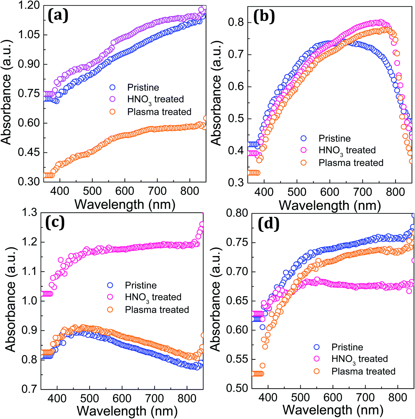 | ||
| Fig. 7 Optical absorption of CdTe films grown on (a) Cu, (b) Al, (c) Ni and (d) SS foil showing the variation due to HNO3 and plasma treatment with respect to pristine substrates. | ||
In the case of CdTe grown on the Cu substrate, HNO3 treatment increased the absorbance and plasma treatment suppressed the magnitude as the morphology change influenced the interaction with photons. Moreover, the characteristics were also not saturated well in the longer wavelength side (∼800 nm).35,46 In contrast, Fig. 7(b) shows well saturated optical absorption obtained from CdTe grown on Al substrates with HNO3 and plasma treatment. Maximum optical absorption in the CdTe films was obtained at the band-edge position in the wavelength scale as shown. In the case of CdTe on the Al substrate, all three CdTe films (pristine, HNO3 and plasma treated) exhibited a similar trend in terms of reaching the maximum and falling in the longer wavelength region as shown in Fig. 7(b). The CdTe film on the Ni substrate showed features similar to CdTe on the Cu substrate but the magnitudes for HNO3 and plasma treatment were higher than the magnitude of absorption occurring in the pristine CdTe film. In this case also, HNO3 treatment yielded better absorbance compared with plasma treated CdTe. In contrast to Cu, Al, and Ni substrates, CdTe films grown on the SS substrate showed improved photo-absorption in the pristine state compared with CdTe grown on HNO3 and plasma treated SS substrates. In conclusion, it was observed that photo-interaction in CdTe is highly sensitive to the morphologies determined by the substrates used to grow CdTe films.35,46 A further change in morphology due to HNO3 and plasma treatment also influenced the absorption significantly. The change in absorption was observed to be very unique depending on substrates and the surface treatments which eventually determine the morphology of the resulting CdTe films. Further, optical bandgap values of the CdTe films were calculated using the Tauc plot method and the values are listed in Table 3.
| Substrates | Optical bandgap (eV) | ||
|---|---|---|---|
| Pristine | HNO3 treated | Plasma treated | |
| Cu | 1.28 | 1.34 | 1.39 |
| Al | 1.43 | 1.46 | 1.48 |
| Ni | 1.39 | 1.35 | 1.37 |
| SS | 1.33 | 1.45 | 1.30 |
Fig. 8 shows the I–V characteristics of the CdTe films grown on (a) Cu, (b) Al, (c) Ni and (d) SS foil showing the variation due to HNO3 and plasma treatment with respect to the pristine substrates measured under dark conditions. The measured current under dark conditions in the CdTe film grown on pristine Cu substrates was lower compared with the current values exhibited by CdTe on Cu substrates subjected to HNO3 and plasma treatment.
 | ||
| Fig. 8 Dark I–V characteristics of the CdTe films grown on (a) Cu, (b) Al, (c) Ni and (d) SS foil showing the variation due to HNO3 and plasma treatment with respect to pristine substrates. | ||
Further, CdTe on Cu with HNO3 treatment resulted in higher current values compared to CdTe on plasma treated Cu. It is evident from the dark I–V values that HNO3 treatment on Cu substrates facilitated charge transport. In the case of CdTe grown on the Al substrate also, HNO3 treatment raised the dark current significantly while the plasma treatment suppressed the same to lower than that for CdTe on the pristine Al substrate as shown in Fig. 8(b). In contrast to CdTe on Cu and Al substrates, the dark current values measured from CdTe on the pristine Ni substrate were higher than the current values obtained from CdTe on the HNO3 and plasma treated Ni substrates as shown in Fig. 8(c). The dark current measured from CdTe on the pristine SS substrate was lower compared with that from CdTe on HNO3 and plasma treated SS substrates as shown in Fig. 8(d). From all these observations, it is inferred that charge transport in CdTe is highly morphology dependent and can further be engineered by surface treatment techniques. Table 4 lists the dark current values obtained from CdTe films coated on Cu, Al, Ni and SS substrates at a 5 V applied bias. In the case of CdTe on Cu and Al, the HNO3 treatment resulted in higher dark current values of 5.67 μA and 1.74 μA, respectively. CdTe on the pristine Ni substrate resulted in a dark current of 29.7 μA and CdTe on the SS substrate showed a maximum dark current of 42.2 μA under the influence of plasma treatment. This shows that each metallic substrate is entirely different in coating CdTe films whose electrical transport characteristics are highly influenced by substrates and further surface treatments.
| Substrates | Dark current (μA) @ 5 V | ||
|---|---|---|---|
| Pristine | HNO3 treated | Plasma treated | |
| Cu | 1.88 | 5.67 | 3.32 |
| Al | 0.41 | 1.74 | 0.03 |
| Ni | 29.7 | 22.1 | 2.13 |
| SS | 3.01 | 26.9 | 42.2 |
Fig. 9 shows the illuminated I–V characteristics of the CdTe films grown on (a) Cu, (b) Al, (c) Ni and (d) SS foil showing the variation due to HNO3 and plasma treatment with respect to pristine substrates. Similar to the dark I–V characteristics, the morphology changes in CdTe films influenced the illuminated I–V characteristics. In the case of CdTe on the Cu substrate, the pristine Cu enabled CdTe to exhibit lower illuminated current compared to CdTe on HNO3 and plasma treated Cu substrates. As demonstrated in the dark I–V characteristics of Al substrates in Fig. 8(b), the illuminated I–V characteristics obtained from CdTe on Al substrates showed the same trend. Fig. 9(c) and (d) confirm that similar features were obtained in illuminated current measured from CdTe on Ni and SS substrates as observed in the case of dark conditions. In general, excess carriers are generated under illumination which as a result exhibited improved current compared to the corresponding dark current values. However, it is essential to consider the electronic quality of the charge transport pathway in CdTe and the morphology at the nanoscale as influential parameters which interact with electrons and holes. While surface treatment increased the current values in CdTe films on the reported four substrates, it is easy to understand that the charge transport pathways are less influenced by defects. The wet-chemical and gas-phase surface treatments energetically modified the morphology which in turn resulted in a change in current. However, it is not simply the same in all four metallic substrates as the morphology undergoes rigorous changes. Thus, it is also essential to consider the morphological effect on charge transport. Table 5 lists all the illuminated current values measured from CdTe films coated on Cu, Ni, Al, and SS substrates measured at a 5 V applied bias. As observed in the dark current values, CdTe on Cu and Al substrates showed higher illuminated current values of 7.9 μA and 2.2 μA, respectively. This similarity between dark and illuminated current values from CdTe on Cu and Al can be attributed to the HNO3 surface treatment on Cu and Al substrates which form good quality CdTe films in which effective charge transport occurred compared to pristine and plasma treated ones. CdTe films on Ni and SS substrates showed higher illuminated current values of 49.8 μA and 73 μA under pristine and plasma treatment. This situation is also very similar to the dark current measured from the CdTe on Ni and SS substrates. Thus, the current values measured under illumination confirm that they are all in good agreement with dark current values.
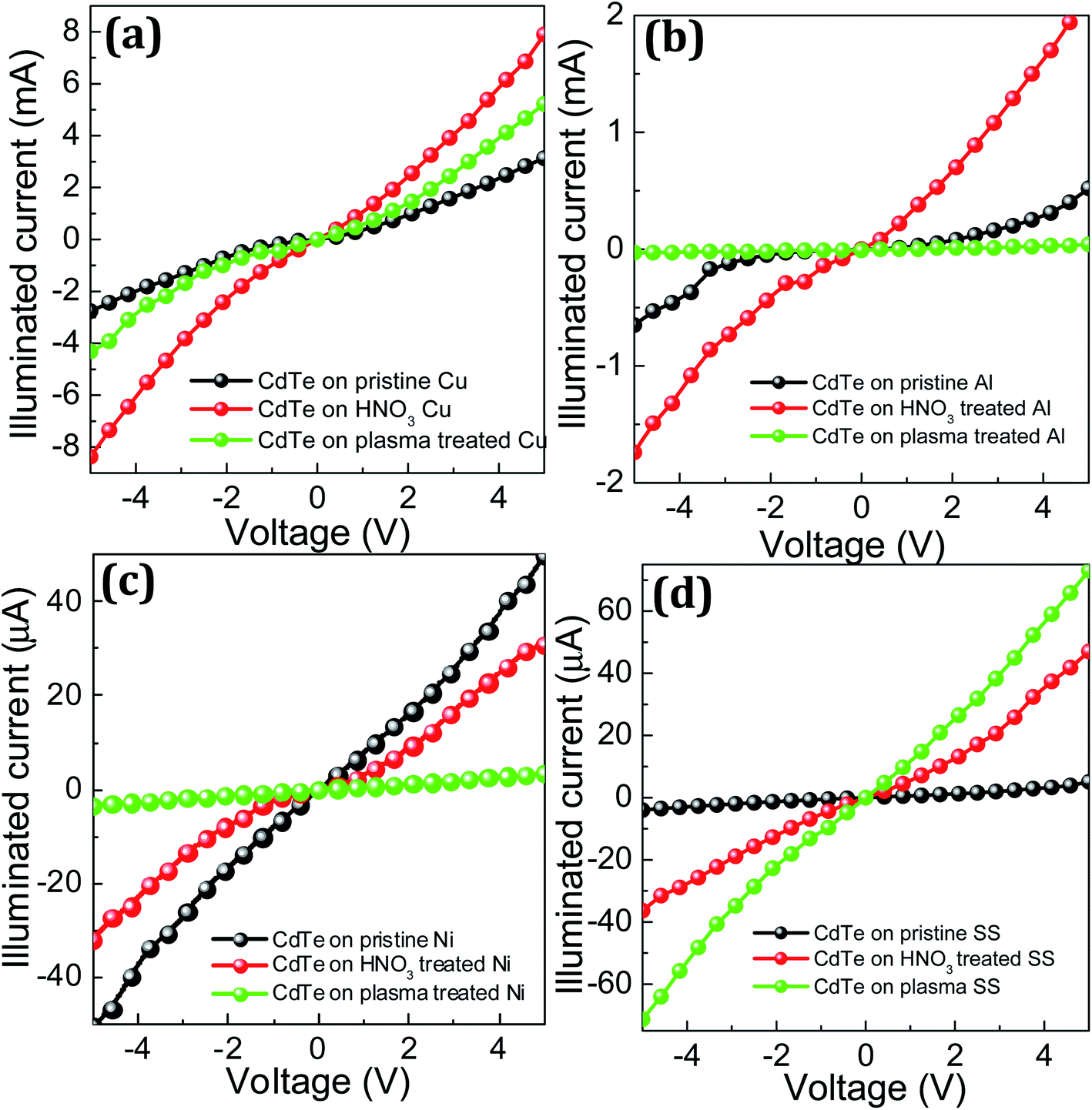 | ||
| Fig. 9 Illuminated I–V characteristics of the CdTe films grown on (a) Cu, (b) Al, (c) Ni and (d) SS foil showing the variation due to HNO3 and plasma treatment with respect to pristine substrates. | ||
| Substrates | Illuminated current (μA) @ 5 V | ||
|---|---|---|---|
| Pristine | HNO3 treated | Plasma treated | |
| Cu | 3.13 | 7.90 | 5.22 |
| Al | 0.52 | 2.21 | 0.04 |
| Ni | 49.8 | 31.0 | 3.14 |
| SS | 5.08 | 47.0 | 73.0 |
The morphological features in functional materials play optically and electronically active roles as they determine light–matter interactions. For example, photon management in textured semiconductor surfaces is entirely different from that in the same semiconductors with a planar surface. Similarly, charge transport in terms of electrons and holes also differs with morphological order. The morphological features in semiconductors directly participate in charge carrier scattering and collision and determine the overall diffusion length which eventually results in the magnitude of the current values measured. The present work accounted for both the change in the morphological order influenced by surface treatment on substrates and, as a result of this, the change in charge transport characteristics. Various possible micro/nanostructures acquired in CdTe due to various approaches/substrates and their influence on physical properties are listed in the ESI section.†
Conclusions
The microstructural characteristics of CdTe films were highly dependent upon the morphology of the metallic foil used as the substrate. Wet-chemical (HNO3) and Ar-plasma modified metal surfaces effectively engineered CdTe growth and resulted in (i) vertically aligned walls, (ii) valley–hills and (iii) micro-granules. Further, studies asserted that the charge transport characteristics in CdTe films were highly influenced by the morphological features as observed from the changes in I–V characteristics both under dark and illuminated conditions.Conflicts of interest
There are no conflicts to declare.Acknowledgements
The authors thank the Amrita Centre for Nanosciences for providing the PVD Cluster facility through industry support to perform CdTe coating and plasma processing on functional materials for energy conversion applications.References
- J. Misiewicz, G. Sęk, R. Kudrawiec and P. Sitarek, Thin Solid Films, 2004, 450, 14–22 CrossRef CAS.
- B. Pasenow, M. Reichelt, T. Stroucken, T. Meier, S. W. Koch, A. R. Zakharian and J. V. Moloney, J. Opt. Soc. Am. B, 2005, 22, 2039–2048 CrossRef CAS.
- K. S. Novoselov, D. Jiang, F. Schedin, T. J. Booth, V. V. Khotkevich, S. V. Morozov and A. K. Geim, Proc. Natl. Acad. Sci. U. S. A., 2005, 102, 10451–10453 CrossRef CAS.
- C. Weisbuch, H. Benisty and R. Houdré, J. Lumin., 2000, 85, 271–293 CrossRef CAS.
- P. Vasa and C. Lienau, ACS Photonics, 2018, 5, 2–23 CrossRef CAS.
- L. Sortino, P. G. Zotev, S. Mignuzzi, J. Cambiasso, D. Schmidt, A. Genco and M. Aßmann, et al. , Nat. Commun., 2019, 10, 1–8 CrossRef CAS.
- L. Britnell, R. M. Ribeiro, A. Eckmann, R. Jalil, B. D. Belle, A. Mishchenko and Y.-J. Kim, et al. , Science, 2013, 340, 1311–1314 CrossRef CAS.
- B. Piccione, C. O. Aspetti, C.-H. Cho and R. Agarwal, Rep. Prog. Phys., 2014, 77, 086401 CrossRef.
- L. Baraban and V. Z. Lozovski, Opt. Spectrosc., 2004, 97, 810–816 CrossRef CAS.
- V. Garg, B. Kamaliya, R. G. Mote and J. Fu, MRS Commun., 2020, 10, 135–140 CrossRef CAS.
- A. Deinega, I. Valuev, B. Potapkin and Y. Lozovik, Opt. Lett., 2010, 35, 106–108 CrossRef.
- G. Köppel, B. Rech and C. Becker, Nanoscale, 2016, 8, 8722–8728 RSC.
- S. J. Cho, T. An and G. Lim, Chem. Commun., 2014, 50, 15710–15713 RSC.
- L. Yao and J. He, Prog. Mater. Sci., 2014, 61, 94–143 CrossRef.
- P. Spinelli, M. A. Verschuuren and A. Polman, Nat. Commun., 2012, 3, 1–5 Search PubMed.
- M. N. Huda and J. A. Turner, J. Appl. Phys., 2010, 107, 123703 CrossRef.
- S.-L. Wu, G.-A. Cheng, R.-T. Zheng and X.-L. Wu, J. Korean Phys. Soc., 2013, 63, 1189–1193 CrossRef CAS.
- E. Menard, A. Marchenko, V. Podzorov, M. E. Gershenson, D. Fichou and J. A. Rogers, Adv. Mater., 2006, 18, 1552–1556 CrossRef CAS.
- F. Nasirpouri, I. Yousefi, E. Moslehifard and J. Khalil-Allafi, Surf. Coat. Technol., 2017, 315, 163–171 CrossRef CAS.
- A. Vasanth, S. V. Nair and M. Shanmugam, Appl. Surf. Sci., 2020, 519, 146263 CrossRef CAS.
- L. Zhang, J. Yang, X. Zhao, X. Xiao, F. Sun, X. Zuo and J. Nan, Chem. Eng. J., 2020, 380, 122546 CrossRef CAS.
- D. Meggiolaro, E. Mosconi, A. H. Proppe, R. Quintero-Bermudez, S. O. Kelley, E. H. Sargent and F. De Angelis, ACS Energy Lett., 2019, 4, 2181–2184 CrossRef CAS.
- T. P. Weiss, B. Bissig, T. Feurer, R. Carron, S. Buecheler and A. N. Tiwari, Sci. Rep., 2019, 9, 1–13 CrossRef CAS.
- S. Yang, C. Zhang, Z. Yang, J. Yao, H. Wang and G. Ding, J. Alloys Compd., 2019, 778, 90–96 CrossRef CAS.
- T. Gu, E.-T. Hu, S. Guo, Y. Wu, J. Wang, Z.-Y. Wang and K.-H. Yu, et al. , Vacuum, 2019, 163, 69–74 CrossRef CAS.
- S. T. Kim, L. Larina, J. H. Yun, B. Shin and B. T. Ahn, Sustainable Energy Fuels, 2019, 3, 709–716 RSC.
- Q. Jiang, Y. Zhao, X. Zhang, X. Yang, Y. Chen, Z. Chu, Q. Ye, X. Li, Z. Yin and J. You, Nat. Photonics, 2019, 13, 460–466 CrossRef CAS.
- W. K. Metzger, S. Grover, D. Lu, E. Colegrove, J. Moseley, C. L. Perkins and X. Li, et al. , Nat. Energy, 2019, 4, 837–845 CrossRef CAS.
- E. Camacho-Espinosa, A. López-Sánchez, I. Rimmaudo, R. Mis-Fernández and J. L. Peña, Sol. Energy, 2019, 193, 31–36 CrossRef CAS.
- K. Shen, Z. Bai, Y. Deng, R. Yang, D. Wang, Q. Li and D. Wang, RSC Adv., 2016, 6, 52326–52333 RSC.
- R. Sekine, M. Uenomachi, H. Asafusa, K. Tokiwa, K. Shimazoe, H. Takahashi, Y. Harada, A. Fujimoto, T. Hirai and S. Sakuragi, Cryst. Growth Des., 2019, 19, 6218–6223 CrossRef CAS.
- Y. Wang, X. Huang, D. Wu, R. Zhuo, E. Wu, C. Jia, Z. Shi, T. Xu, Y. Tian and X. Li, J. Mater. Chem. C, 2018, 6(18), 4861–4865 RSC.
- M. Shaygan, K. Davami, N. Kheirabi, C. K. Baek, G. Cuniberti, M. Meyyappan and J.-S. Lee, Phys. Chem. Chem. Phys., 2014, 16, 22687–22693 RSC.
- X. Xie, S.-Y. Kwok, Z. Lu, Y. Liu, Y. Cao, L. Luo and J. A. Zapien, et al. , Nanoscale, 2012, 4, 2914–2919 RSC.
- L. K. Jambi, J. E. Lees, S. L. Bugby, S. Tipper, M. S. Alqahtani and A. C. Perkins, J. Instrum., 2015, 10, P06012 CrossRef.
- M. Powalla, S. Paetel, E. Ahlswede, R. Wuerz, C. D. Wessendorf and T. Magorian Friedlmeier, Appl. Phys. Rev., 2018, 5, 041602 Search PubMed.
- C. K. Miskin, A. Dubois-Camacho, M. O. Reese and R. Agrawal, J. Mater. Chem. C, 2016, 4, 9167–9171 RSC.
- S. Kumar and K. S. R. Koteswara Rao, Energy Environ. Sci., 2014, 7, 45–102 RSC.
- J. C. Quiñones-Galván, A. Guillén-Cervantes, E. Campos-González, J. Santos-Cruz, S. A. Mayén-Hernández, M. de la L. Olvera, O. Zelaya-Angel, G. Contreras-Puente and F. de Moure-Flores, J. Laser Appl., 2016, 28, 032012 CrossRef.
- A. M. Ali, K. S. Rahman, L. M. Ali, M. Akhtaruzzaman, K. Sopian, S. Radiman and N. Amin, Results Phys., 2017, 7, 1066–1072 CrossRef.
- B. E. McCandless and J. R. Sites, Handbook of Photovoltaic Science and Engineering, 2011, pp. 600–641 Search PubMed.
- A. Bosio, N. Romeo, S. Mazzamuto and V. Canevari, Prog. Cryst. Growth Charact. Mater., 2006, 52, 247–279 CrossRef CAS.
- A. Morales-Acevedo, Sol. Energy, 2006, 80, 675–681 CrossRef CAS.
- J. L. Plaza, O. Martínez, S. Rubio, V. Hortelano and E. Diéguez, CrystEngComm, 2013, 15, 2314–2318 RSC.
- J. M. Lugo, E. Rosendo, R. Romano-Trujillo, A. I. Oliva, H. Pérez Ladrón de Guevara, C. I. Medel-Ruiz and L. Treviño-Yarce, et al. , Mater. Res. Express, 2019, 6, 076428 CrossRef CAS.
- S. L. Patel, S. Chander, M. D. Kannan and M. S. Dhaka, Appl. Surf. Sci., 2019, 498, 143824 CrossRef CAS.
- D. Zhou, M. Lin, Z. Chen, H. Sun, H. Zhang, H. Sun and B. Yang, Chem. Mater., 2011, 23, 4857–4862 CrossRef CAS.
- J.-H. Yang, W.-J. Yin, J.-S. Park, J. Ma and S.-H. Wei, Semicond. Sci. Technol., 2016, 31, 083002 CrossRef.
- D. Krasikov and I. Sankin, J. Mater. Chem. A, 2017, 5, 3503–3513 RSC.
- J. M. Burst, S. B. Farrell, D. S. Albin, E. Colegrove, M. O. Reese, J. N. Duenow, D. Kuciauskas and W. K. Metzger, APL Mater., 2016, 4, 116102 CrossRef.
- I. M. Dharmadasa, Coatings, 2014, 4, 282–307 CrossRef.
- V. Komin, B. Tetali, V. Viswanathan, S. Yu, D. L. Morel and C. S. Ferekides, Thin Solid Films, 2003, 431, 143–147 CrossRef.
- S. Yao, L. Liu, Q. Zeng, X. Du, C. Im, Y. Liu, H. Zhang, B. Yang, T. Cui and W. Tian, J. Mater. Chem. C, 2018, 6(41), 11156–11161 RSC.
- M. O. Reese, J. M. Burst, C. L. Perkins, A. Kanevce, S. W. Johnston, D. Kuciauskas, T. M. Barnes and W. K. Metzger, IEEE J. Photovolt., 2014, 5, 382–385 Search PubMed.
- G. I. García-Alvarado, F. de Moure-Flores, S. A. Mayén-Hernández, D. Santos-Cruz, E. M. Rivera-Muñoz, G. S. Contreras-Puente, M. Pal and J. Santos-Cruz, Vacuum, 2017, 142, 175–180 CrossRef.
- M. Arreguín-Campos, K. Gutiérrez ZB, J. G. Quiñones-Galván, J. Santos-Cruz, S. A. Mayén-Hernández, O. Zelaya-Angel, M. de la L. Olvera, G. Contreras-Puente and F. de Moure-Flores, J. Electron. Mater., 2019, 48, 3595–3602 CrossRef.
Footnote |
| † Electronic supplementary information (ESI) available. See DOI: 10.1039/d0na00532k |
| This journal is © The Royal Society of Chemistry 2020 |