
 Open Access Article
 This Open Access Article is licensed under a Creative Commons Attribution-Non Commercial 3.0 Unported Licence
Barrier-assisted vapor phase CVD of large-area MoS2 monolayers with high spatial homogeneity†
Santhosh
Durairaj
a,
P.
Krishnamoorthy
a,
Navanya
Raveendran
a,
Beo Deul
Ryu
b,
Chang-Hee
Hong
b,
Tae Hoon
Seo
c and
S.
Chandramohan
 *a
*a
a2D Materials and Devices Laboratory, Department of Physics and Nanotechnology, SRM Institute of Science and Technology, Kattankulathur, 603 203, Tamil Nadu, India. E-mail: chandras3@srmist.edu.in; scmphysics@gmail.com
bDepartment of Semiconductor Science and Technology, Semiconductor Physics Research Center, Chonbuk National University, Jeonju 54896, South Korea
cSmart Energy & Nanophotonics R&D Group, Korea Institute of Industrial Technology, Gwangju 61012, South Korea
First published on 9th July 2020
Abstract
Atomically thin molybdenum disulphide (MoS2) is a direct band gap semiconductor with negatively charged trions and stable excitons in striking contrast to the wonder material graphene. While large-area growth of MoS2 can be readily achieved by gas-phase chemical vapor deposition (CVD), growth of continuous MoS2 atomic layers with good homogeneity is indeed one of the major challenges in vapor-phase CVD involving all-solid precursors. In this study, we demonstrate the growth of large-area continuous single crystal MoS2 monolayers on c-plane sapphire by carefully positioning the substrate using a facile staircase-like barrier. The barrier offered great control in mitigating the secondary and intermediate phases as well as second layer nucleation, and eventually a continuous monolayer with high surface homogeneity is realized. Both micro-Raman and high-resolution transmission electron microscopy (HRTEM) results confirmed the high structural quality of the grown MoS2 layers. Using low temperature photoluminescence spectroscopy, additional pieces of information are provided for the strong band-edge emission in the light of vacancy compensation and formation of Mo–O bonding. The monolayer MoS2 transferred to SiO2/Si exhibited a room temperature field-effect mobility of ∼1.2 cm2 V−1 s−1 in a back-gated two-terminal configuration.
Introduction
Two-dimensional (2D) layered materials are currently at the forefront of various research areas due to their unprecedented properties. Graphene, the first 2D material experimentally realized, has already undergone manifold theoretical and experimental investigations during the last one decade for application in various fields.1–3 Meanwhile, several other 2D layered materials have been predicted and some are realized experimentally, paving the way for advanced devices with greater functionalities.2,3 Unlike graphene, monolayer transition metal dichalcogenides (TMDCs) such as MoS2, WS2, and WSe2 offer a finite direct band gap, thus showing great potential for application in nano-electronic and optoelectronic devices.4,5 Molybdenum disulphide (MoS2) is one of the TMDCs of current research focus. In MoS2, Mo atoms are sandwiched between two sulfur atoms (S–Mo–S) by a strong covalent bond in one of the three structural polytypes, subject to the coordination models between the metal and the chalcogen atoms and stacking orders between the layers. One of the intriguing characteristics of MoS2 is the transformation of the optical band gap from indirect (1.2 eV) to direct (1.85 eV) nature with decreasing layer numbers from bulk to the monolayer.6 In addition, monolayer MoS2 differs from graphene in two aspects; the first is lack of inversion symmetry which leads to high inter-band transition at the K-point due to the valley dependent optical selection rule and the second is the strong spin–orbital coupling in the d-orbital system.7 Hence, monolayer MoS2 is considered a potential candidate material for various opto-electronic device applications.8Continuous MoS2 films with high spatial homogeneity over large areas are the ideal materials for realizing practical devices. Both mechanical9 and liquid phase exfoliation10,11 methods are not suitable for electronic device applications because these methods only offer flakes of nano- to micro-meter sizes with poor layer controllability. Alternatively, chemical vapor deposition (CVD) is proven to be a suitable method to grow single crystal MoS2 with layer controllability and homogeneity over large area.12–14 Based on the type of precursor used, CVD reactions can be classified as gas phase and vapor phase, and most of the current CVD based MoS2 production uses either of these two methods. In the gas phase CVD approach, pyrolysis of Mo based hexacarbonyl or organometallic compounds and hydrogen sulphide (H2S) occurs on the substrate in a reaction chamber, resulting in continuous MoS2 on a wafer scale with atomically smooth surfaces.14–17 Though this method is considered promising for the growth of wafer-scale MoS2, the high price of the Mo precursors and the need for safety systems to handle certain toxic precursors make this method costly and environmentally not benign. Alternatively, the use of solid phase precursors such as molybdenum trioxide (MoO3) and sulfur to grow MoS2 films has attracted significant attention as these precursors are environmentally friendly and the growth setup is simple and relatively low cost.12,18,19 Yet another promising feature of this method compared to gas-phase CVD is the ability to achieve larger size grains (up to a few hundreds of micrometers).20 In fact, this method has been found to be highly effective in achieving rapid growth of other TMDCs such as WS2 and WSe2 on Au foils.21,22 Recently, growth of 6 inch uniform MoS2 on a glass substrate has been demonstrated via a Mo foil-assisted face-to-face metal precursor supply strategy in a vapor-phase CVD process, exploiting the homogeneously distributed Na catalysts in the glass.23 However, as far as the growth on other substrates is concerned using all-solid precursors, difficulty in controlling the vapor flux (associated with the large difference in the evaporation temperatures of Mo and S source materials) poses challenges in achieving a continuous monolayer MoS2 film without secondary or intermediate phases viz. molybdenum dioxide (MoO2) and molybdenum oxysulphide (MoOS2). These secondary phases have been observed to be present on the surface of MoS2 films grown by vapor phase CVD.24 Several approaches have been used to obtain continuous, large area MoS2, but no control over the formation of secondary phases is realized. Pondick et al.24 reported that both MoO2 and MoOS2 are intermediate products in a reaction resulting due to variations in the local Mo![[thin space (1/6-em)]](https://www.rsc.org/images/entities/char_2009.gif) :S vapor ratio on the substrate. Though this study has shown a way to convert MoOS2 into MoS2via extended sulfurization by keeping the S:Mo molar ratio well in excess than the stoichiometric requirement, the formation of continuous monolayer MoS2 was not demonstrated. To effectively control the precursor reaction rate, Lim et al.25 used nickel oxide (NiO) foam as a reactive-barrier between the MoO3 source and the substrate. In this case, the NiO reacts with the MoO3 and forms nickel(II) molybdate (NiMoO4) all along the vapor trajectory in the NiO foam, which eventually controls the Mo concentration gradient. The use of the NiO reactive barrier facilitated the growth of larger grains of ∼170 μm in size on a c-plane sapphire substrate, but yet the sample contained a significant amount of secondary phases such as MoO3−x. Recently, the use of independent carrier gas pathways and addition of oxygen led to successful wafer-scale epitaxial growth of continuous MoS2 on sapphire.26 Besides the growth of wafer-scale MoS2 films, a facile method for growing TMDC monolayers with high spatial homogeneity across a large area is highly desired for further scale-up synthesis.
:S vapor ratio on the substrate. Though this study has shown a way to convert MoOS2 into MoS2via extended sulfurization by keeping the S:Mo molar ratio well in excess than the stoichiometric requirement, the formation of continuous monolayer MoS2 was not demonstrated. To effectively control the precursor reaction rate, Lim et al.25 used nickel oxide (NiO) foam as a reactive-barrier between the MoO3 source and the substrate. In this case, the NiO reacts with the MoO3 and forms nickel(II) molybdate (NiMoO4) all along the vapor trajectory in the NiO foam, which eventually controls the Mo concentration gradient. The use of the NiO reactive barrier facilitated the growth of larger grains of ∼170 μm in size on a c-plane sapphire substrate, but yet the sample contained a significant amount of secondary phases such as MoO3−x. Recently, the use of independent carrier gas pathways and addition of oxygen led to successful wafer-scale epitaxial growth of continuous MoS2 on sapphire.26 Besides the growth of wafer-scale MoS2 films, a facile method for growing TMDC monolayers with high spatial homogeneity across a large area is highly desired for further scale-up synthesis.
The present study is therefore focused on understanding the position dependence of the MoS2 growth via process optimization in realizing continuous monolayer MoS2 with high spatial homogeneity and electronic quality without any secondary or intermediate phases. The novelty of our study lies in the use of SiO2 as a mechanical barrier to moderate the Mo flux so as to allow better controllability and high position selectivity for the growth of homogeneous MoS2 monolayers. The study also uncovers the potential of the oxide barrier substrate as a possible source of oxygen, which plays an important role in enhancing the photoluminescence of MoS2. A high-resolution transmission electron microscopy (HRTEM) study provided direct evidence for the formation of single crystal MoS2 with hexagonal symmetry (2H). For a fixed Mo:S precursor ratio, the density of secondary phases in the sample showed high position dependence. Raman, photoluminescence, and X-ray photoelectron spectroscopic techniques were used to verify the number of layers, crystal and optical quality, and chemical environment of the grown MoS2 layers. Electrical measurements using two terminal circular transfer length method (CTLM) test structures showed space charge limited current (SPLC) transport at high applied voltages. The method demonstrated in this study can be extended to grow other TMDCs by vapor-phase CVD using all-solid precursors.
Experimental section
Growth of MoS2
The growth of MoS2 was performed in a three-zone CVD system using solid precursors under a continuous flow of argon gas. In a typical experiment, 200 mg of sulfur powder (99.9%, Alfa Aesar) and 10 mg of MoO3 powder (99.999%, Alfa Aesar) were taken in two separate ceramic boats and placed inside a quartz tube with a distance of separation of 45 cm. The substrate for the growth, c-plane (0001) sapphire, was placed above the MoO3 powder on SiO2/Si barriers, as illustrated in Fig. 1. Prior to the growth, the tube was evacuated and purged with argon gas three times. The flow rate of argon gas in all our experiments was set at 200 sccm. The temperature of the sulfur and MoO3 precursor zones was set at 180 °C and 700–800 °C, respectively. The temperature of the zone where MoO3 was placed was gradually increased at a rate of 7 °C per minute. The other zone where the sulfur was placed was set to a temperature of 180 °C. The heating rate of this zone was calculated based on the temperature ramp time of the high temperature zone. After a dwell time of 10 minutes, the reactor was allowed to cool down to room temperature.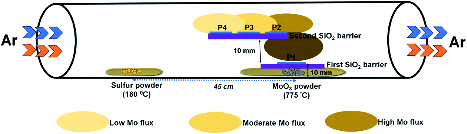 | ||
| Fig. 1 Schematic of the experimental setup showing the side-view geometry of the stair-case-like barrier and different substrate positions discussed in this work. | ||
Characterization and device fabrication
An Olympus optical microscope was used to obtain the microscopic picture of the MoS2 surface. The images were captured using a 100× objective (numerical aperture of 0.90). Room temperature micro-Raman spectra were acquired using a HORIBA LabRAM HR evolution spectrometer. All the spectra reported were recorded in backscattering geometry using a solid-state laser with a 532 nm excitation wavelength. The laser power and the spot size used were 5 mW and 1 μm, respectively. PL measurements were carried out on a micro-Raman spectrometer using a He–Cd laser (325 nm) as the excitation source. The surface topography of the MoS2 film was studied using an atomic force microscope (Park Systems, Korea) in tapping mode. The optical absorbance of the films (on the two-side polished sapphire substrate) was studied using a UV-Vis-NIR spectrometer (Agilent, Cary 5000). HRTEM analysis of the grown MoS2 layer was performed using an aberration-corrected electron microscope (JEOL-3010, JEOL, Japan) with a 0.14 nm lattice resolution and 0.12 nm point to point resolution. X-ray photoelectron spectroscopic analyses were performed using a K-Alpha ESCA System (Thermo Scientific) with an Al Kα (1486.6 eV) X-ray source. Circular TLM and FET devices were fabricated by photolithography followed by metal deposition in a clean room. In a typical CTLM fabrication process, the MoS2 sample coated with a negative photoresist was exposed to the i-line (365 nm) through a Cr mask for pattern transfer. The CTLM pattern consisted of ring patterns of varying widths from 5 μm to 45 μm. This was followed by the development step and Ti/Au deposition. For the FET fabrication, the MoS2 film was transferred from sapphire to p++ silicon with a resistivity of 0.01 ohm cm capped with 295 nm thermally grown SiO2. In a typical transfer process, polymethylmethacrylate (PMMA, MW ∼ 350k) dissolved in anisole was spin coated at 2000 rpm for 30 s. The MoS2 film was then detached in 2 wt% KOH solution at 70 °C for 2 hours and then transferred to successive DI water baths to ensure complete removal of any chemical residues. The floating MoS2 film was transferred to the desired substrate and baked for 2 hours at 70 °C. PMMA was removed by immersing the sample in an acetone bath for 2 hours. Back-gated FET devices were defined by photolithography with Ti/Au (30/100 nm) metal as source and drain contact electrodes. I–V measurements were performed using a LakeShore (Model: PS100) Probe Station and a semiconductor parameter analyzer (Keithley 5200A) at room temperature after evacuating the chamber to a pressure of 5 × 10⁻² mbar.Results and discussion
The experimental setup used for the growth of MoS2 is schematically illustrated in Fig. 1. Unlike previously reported approaches, where the substrate is placed upside-down directly on the Mo precursor,27 we used a SiO2/Si substrate as a barrier between the sapphire (growth substrate) and the Mo precursor, and the substrate was placed facing upward. The purpose of this SiO2 substrate is to limit the Mo vapor concentration at the substrate position so as to avoid the formation of secondary or intermediate phases. It also helps to understand the position dependence of the growth with respect to the substrate position, as the concentration gradient arises around the Mo source due to the temperature gradient. From the Mo source position towards the upstream direction, there are three different zones with decreasing Mo flux, as emphasized in Fig. 1. Fig. 2a–c show the optical microscopy images of MoS2 grown at 775 °C on sapphire by placing the substrate at position P1 on the first SiO2 barrier (refer to Fig. 1 to visualize the position and see the ESI Fig. S1–S4† for the effect of different growth temperatures). The optical images acquired from different regions of the sample show the presence of grey rod-like structures and white and black particles on the surface. The observed rod-like structures in Fig. 2a are identified as intermediate species of MoOS2 by micro-Raman spectroscopy (discussed later), similar to the results reported in ref. 28. It is also observed from the optical images that the local variations in the density of such intermediate species are dependent on the lateral position of the substrate from the Mo precursor. The edge of the substrate which receives the Mo vapor flux first is always found to have higher density of intermediate species. In our experiment, Mo vapors diffuse out from both ends of the substrate, leading to the formation of more intermediate phases on either edge of the substrate along the tube direction, which can be inferred from the colour contrast of the sample shown in Fig. 2d. Raman spectroscopy is a useful tool for qualitative determination of various phases present in the material at the micrometer scale. Fig. 2e shows the Raman spectra obtained for different positions where each spectrum corresponds to the circled position in Fig. 2c with the same colour. The results show the presence of secondary phases such as MoO2 and MoOS2 on the surface of MoS2 with MoOS2 being the predominant intermediate phase. The spectrum corresponding to cubic particles shows several peaks; the peaks observed at frequencies below 500 cm−1 match with the stretching modes of oxygen atoms doubly coordinated with Mo atoms (Mo–O–Mo) and the peaks at 574, 594, and 748 cm−1 match with the stretching modes of oxygen terminated Mo, indicating the presence of MoO2 crystals in the grown sample.29 The spectrum corresponding to rod-like structures reveals additional peaks in the frequency range from 384–405 cm−1, characteristic of Mo![[double bond, length as m-dash]](https://www.rsc.org/images/entities/char_e001.gif) S and S–S vibrations in MoOS2.24 On the other hand, the spectrum obtained from the smooth region shows the characteristic Raman modes of 2H-MoS2, the in-plane-vibration longitudinal optical (LO) phonon mode E12g at 384.2 cm−1 and the out-of-plane-vibration transverse optical (TO) phonon mode A1g at 404.1 cm−1. The frequency difference (Δω) of 19.9 cm−1 between the two modes confirms the formation of monolayer MoS2.30
S and S–S vibrations in MoOS2.24 On the other hand, the spectrum obtained from the smooth region shows the characteristic Raman modes of 2H-MoS2, the in-plane-vibration longitudinal optical (LO) phonon mode E12g at 384.2 cm−1 and the out-of-plane-vibration transverse optical (TO) phonon mode A1g at 404.1 cm−1. The frequency difference (Δω) of 19.9 cm−1 between the two modes confirms the formation of monolayer MoS2.30
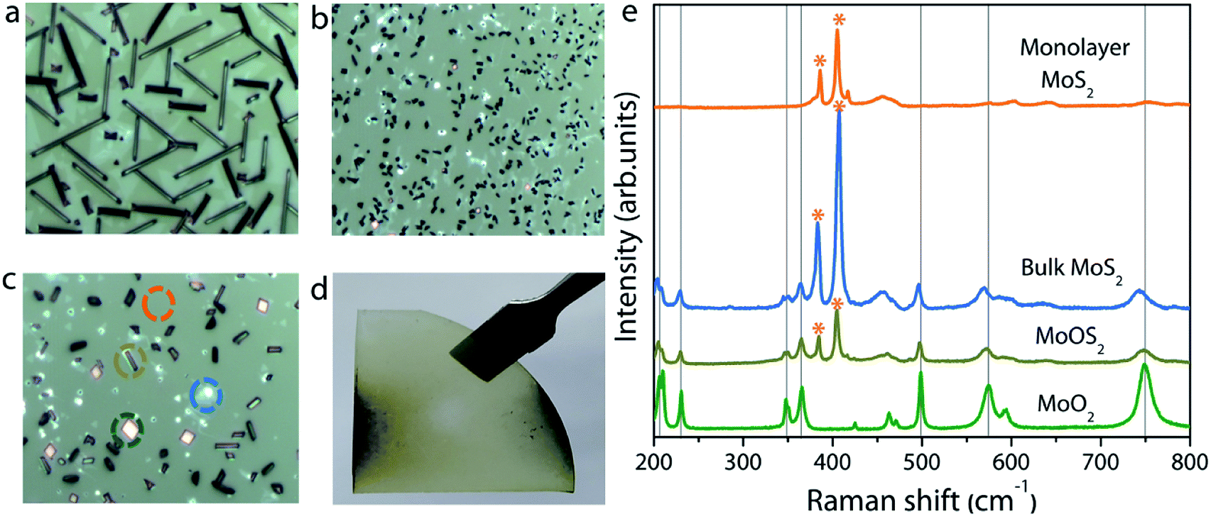 | ||
| Fig. 2 (a–c) Optical microscopy images of the sample in three different regions from left to right in (d). (d) Photograph of a typical sample grown at position P1. (e) Raman spectra of the grown sample at different positions circled in (c) indicating the presence of MoO2, MoOS2, bulk, and monolayer MoS2. | ||
In addition to continuous monolayer formation, the sample showed the formation of bulk MoS2 at random sites, which is also evident from the Raman spectrum. In the case of bulk MoS2, the E12g mode is shifted towards lower frequency because of long range coulombic interaction force causing the bond length of MoS atoms to increase while the A1g mode is shifted towards higher frequency due to enhanced restoring force between interlayer S–S bonds.30 The value of Δω in this case is estimated to be 24.5 cm−1, thus confirming the bulk nature of the MoS2 in accordance with previous findings.31 The observed secondary or intermediate phases on the MoS2 monolayer are detrimental to the device fabrication. A second barrier is therefore introduced above the first barrier in the form of a staircase to eliminate the secondary phase formation via controlling the Mo flux at the substrate position. Fig. 3a–i show the optical images of MoS2 grown by placing the substrate on the second barrier at three different positions (positions P2, P3, and P4 shown in Fig. 1). It is observed that the sample grown by placing the substrate at position P2 still contains traces of secondary phases, but their density is relatively lower compared to that of the sample grown at P1. This result can be understood by considering the high amount of MoO3 vapors expected at the edge of the barrier. So, the substrate was moved towards the upstream direction in the reactor to position P3 and P4 to understand the growth behaviour. At first sight, the sample grown at position P3 seems to be homogeneous and no obvious colour contrast is seen within the entire grown area (refer to the photograph of the corresponding sample shown on the right). The optical images (Fig. 3d–f) of the sample taken at different points give further indication that the MoS2 film is homogeneous on the entire substrate without any secondary or intermediate phases. A further change in the substrate position more towards the upstream direction (at position P4) also provided similar results, except that there was some discontinuity in the film at random sites. In particular, the upstream edge of the substrate had isolated and merged triangular grains (Fig. 3i). Thus, it is presumable that the staircase barrier helped to prevent the direct deposition of secondary phases on the substrate at elevated growth temperature. Also, an increase in the lateral distance between the precursor and the substrate limits the amount of Mo vapors available at the substrate position for the reaction to occur. In all the cases, the Mo:S ratio is fixed to a value of 1:20 and the high sulfur content facilitates complete conversion of intermediate phases to MoS2, leading to a homogeneous film formation. The Raman spectrum of the corresponding sample in Fig. 4a shows peaks corresponding to E12g and A1g at 386.2 and 404.1 cm−1, respectively. Once again, the Δω of 18.9 cm−1 between the two modes suggests the formation of monolayer MoS2. Furthermore, the full width at half maximum (FWHM) of the Raman peak, a figure-of-merit for the qualitative evaluation of the quality of the crystalline structures, is estimated to be 2.9 and 4.2 cm−1, respectively, for the E12g and A1g peaks. These values fall within the range reported for mechanically exfoliated single crystal MoS2, signifying the respectable quality of the grown MoS2 layers.32 The spatial homogeneity of the grown MoS2 films is also studied by mapping the positions of the two Raman modes (E12g and A1g) over an area of 30 × 30 μm2 (see also ESI Fig. S5† for the Raman spectrum at various points over the entire substrate). One can visualize from Fig. 4b and c that the frequencies of the two modes are constant at every point the spectrum is acquired with maximum deviation of 0.263 cm−1 and 0.122 cm−1, respectively, for the E12g and A1g modes. This result gives further evidence for the homogeneous and monolayer nature of the grown MoS2 layers.
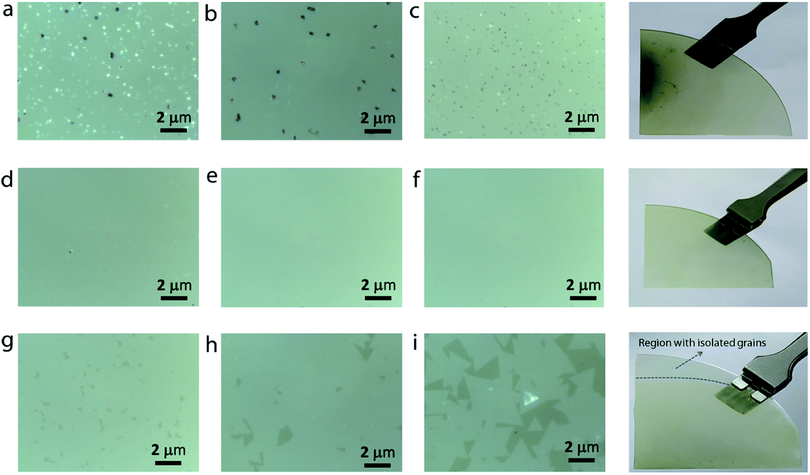 | ||
| Fig. 3 Optical microscopy images of the MoS2 sample grown at substrate positions P2 (a–c), P3 (d–f) and P4 (g–i). The three images for each sample are acquired from left, middle, and right portions of the sample. The photographs of the corresponding samples are given on the right. | ||
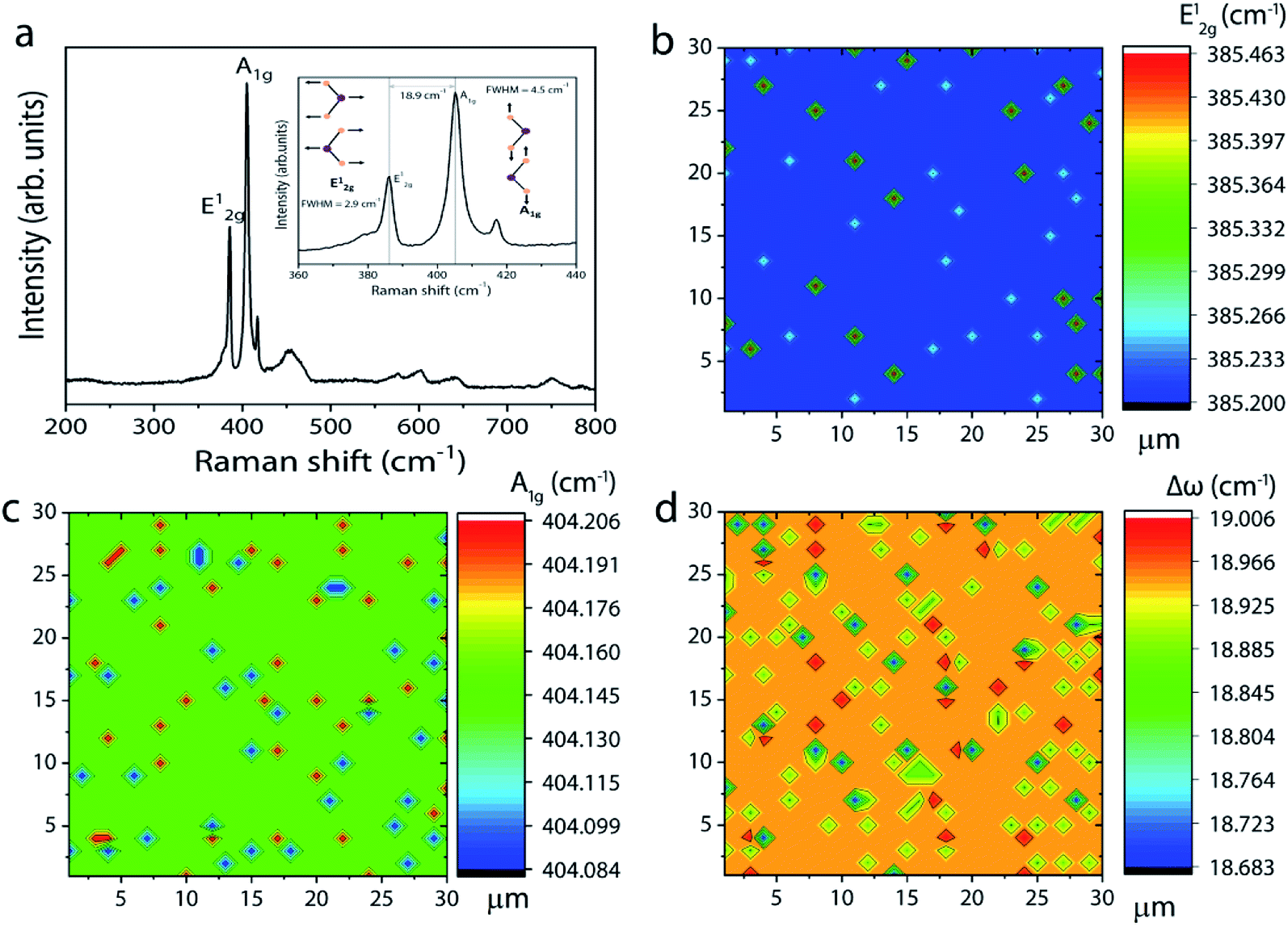 | ||
| Fig. 4 (a) Raman spectrum of MoS2 monolayers grown at position P3. The inset shows the same spectrum for E12g and A1g modes. (b–d) Raman mapping results for E12g, A1g and Δω frequencies obtained over 30 × 30 μm2. | ||
The crystal quality and phase purity of the MoS2 film are further evaluated with the help of high-resolution transmission electron microscopy (HR-TEM). Fig. 5a shows the low-magnification TEM image of a portion of the sample on a TEM grid. One can clearly see the continuous film with some layer folding, which is inherent to the transfer process. The selected area electron diffraction (SAED) pattern shown in Fig. 5b confirms the single crystalline quality of the grown MoS2 layer (see Fig. S6 in the ESI† for SAED patterns obtained from different regions of the sample). Furthermore, the HRTEM image (Fig. 5c) taken at a random site shows the crystal lattice composed of hexagonal rings. Fig. 5d shows the surface topography of typical monolayer MoS2 grown at position P3. The surface is found to be smooth and homogeneous with a root mean square surface roughness of 0.443 nm. Furthermore, the thickness of the film is estimated to be ∼0.8 nm (see ESI Fig. S7†), which is close to the value expected for three atom thick monolayer MoS2.27
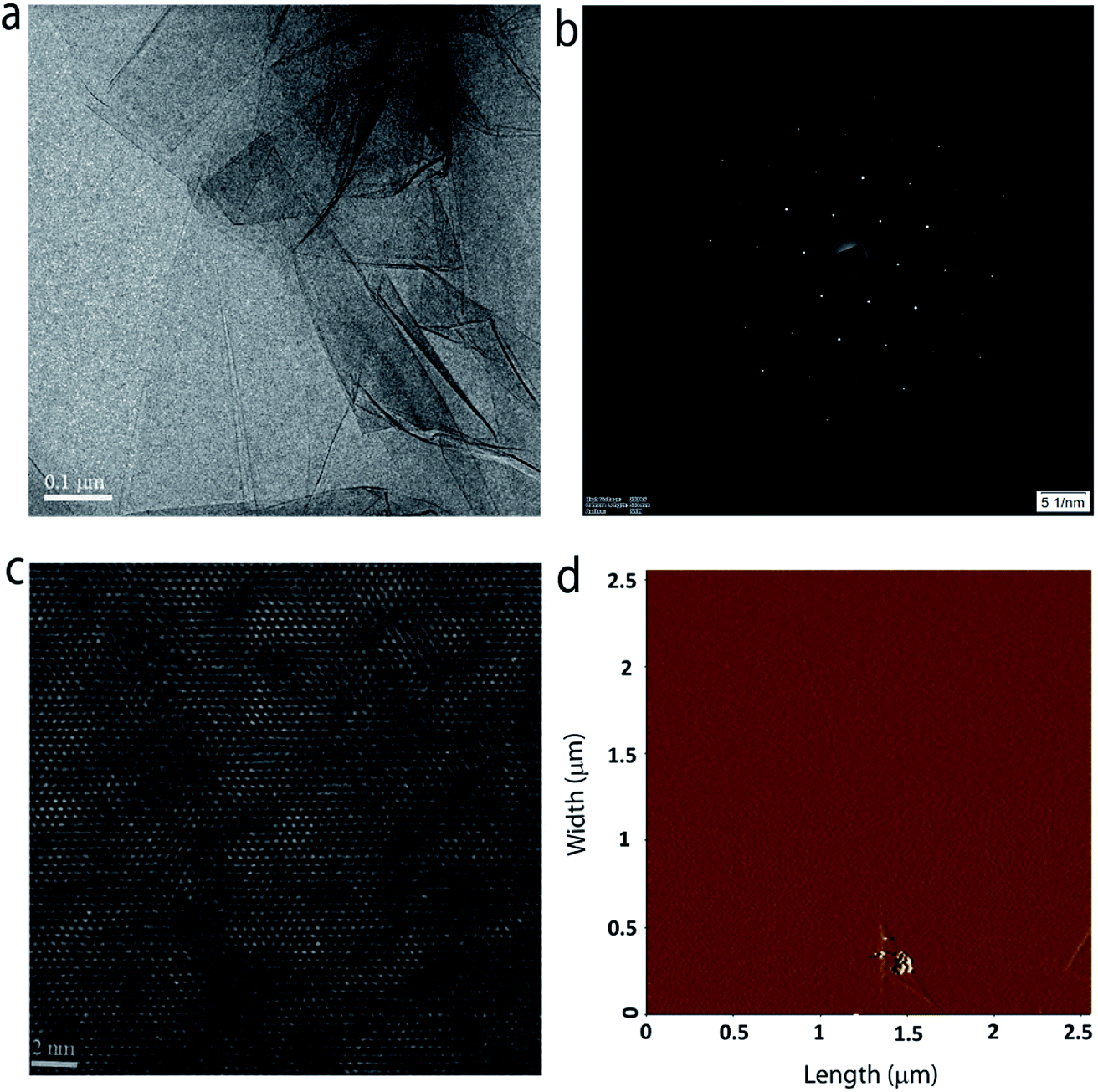 | ||
| Fig. 5 (a) TEM image of the MoS2 film transferred on to a copper grid. (b) SAED pattern indicating the single crystal nature of the grown MoS2 film. (c) HRTEM image of the same sample showing the hexagonal structure. (d) AFM surface topography of the grown MoS2 film. | ||
Photoluminescence measurements were carried out on the MoS2 sample grown under optimum conditions. The room-temperature PL spectrum shown in Fig. 6a is characterized by a single strong peak at 1.89 eV, which is attributed to the so-called radiative recombination of neutral A excitons in monolayer MoS2.6 The low temperature photoluminescence is a unique spectroscopic tool to evaluate the structural defects in semiconducting materials. Fig. 6b shows the PL spectra of a typical monolayer MoS2 film recorded at different temperatures from 93 K to 273 K. It is observed that the intensity of the free exciton or band edge (X0) emission increases with decreasing temperature due to better exciton–phonon coupling. Moreover, the exciton peak red shifts as temperature increases due to band gap reduction, a typical trend well described by the Varshni equation for many semiconductors.33,34 For MoS2, in addition to the free exciton peak, an additional peak at low energy around 1.75 eV arises if bound exciton (Xb) states are present.33–35 If excitons are not tightly bound to defects, they can be easily perturbed by thermal stimulation, and hence a peak evolve at low temperatures. In other words, since the probability for nonradiative recombination increases with temperature, the defect-induced bound exciton peak will quench at room temperature. However, it is interesting to note that the bound exciton peak is not manifest in the spectra even at low temperatures. According to a study reported by Haiyan Nan et al.,36 oxygen molecules adsorbed on sulfur vacancy sites in the MoS2 lattice could enhance the radiative recombination via trion-to-exciton conversion and quenching of nonradiative recombination at defect sites (sulfur vacancy sites). As our MoS2 samples showed the presence of Mo–O bonding (will be discussed later), the observed strong photoluminescence and the absence of bound exciton peaks both could be taken as a measurement parameter for the high optical quality of the MoS2 film. The spatial homogeneity of the sample is further examined by mapping the PL intensities over an area of 50 × 50 μm2. Fig. 6c gives a clear picture of the thickness and spatial homogeneity of the grown MoS2. To supplement the PL results, the optical absorption spectrum of the MoS2 layer is recorded and the result is shown in Fig. 6d. The spectrum clearly shows three absorption peaks at 1.89, 2.05, and 2.89 eV, corresponding to A, B, and C excitons, respectively. These bands originate from the direct band gap transition in monolayer MoS2 at the K-point due to spin–orbital coupling induced energy level splitting in the valence band.6 The energy difference between A and B excitonic peaks is estimated to be 0.16 eV. It is interesting to note that for monolayer MoS2 with a high crystal quality and fine electronic structure, this value is reported to be approximately 0.148 eV based on theoretical calculations.17,37,38 The above result therefore leads us to conclude that the MoS2 layers grown in this work are of excellent quality, consistent with the HRTEM and PL results.
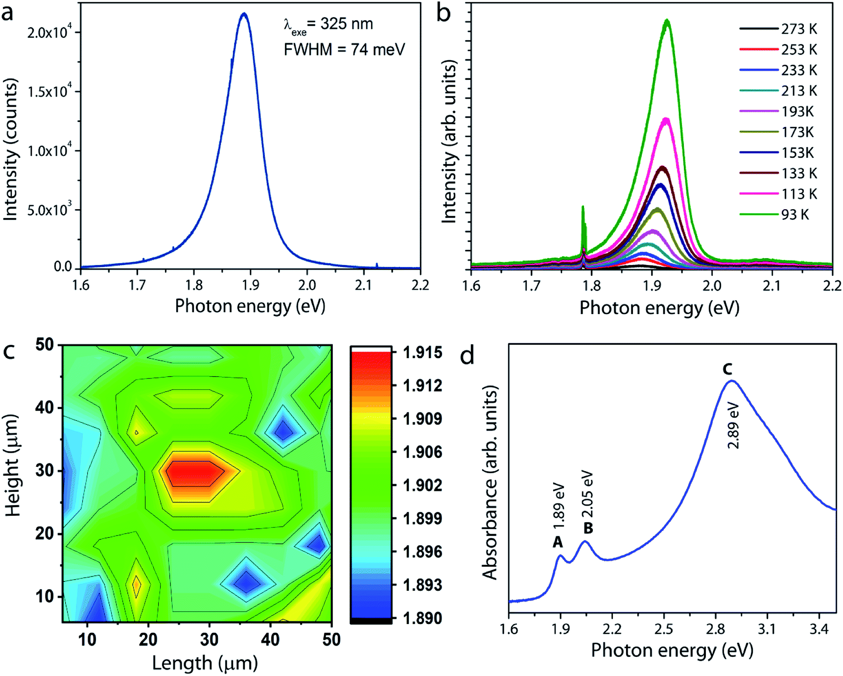 | ||
| Fig. 6 (a) Room temperature photoluminescence spectrum of MoS2 under excitation at 325 nm. (b) Temperature-dependent photoluminescence spectra of the MoS2 film. (c) PL mapping for the peak emission wavelength scanned over a 50 × 50 μm2 area. (d) Absorption spectrum of monolayer MoS2. | ||
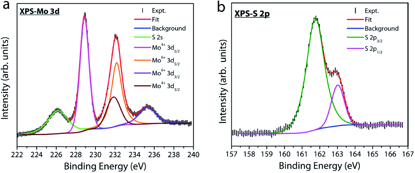
X-ray photoelectron spectroscopy (XPS) measurements were performed under UHV conditions to examine the atomic composition and nature of the chemical bonding in our MoS2 samples. Fig. 7a displays the Mo 3d core level spectrum where the experimental data are fitted with four peaks at a binding energy of 228.8, 231.8, 232.1 and 235.2 eV. The first two peaks, located at lower binding energies, represent the doublet component Mo 3d5/2 and Mo 3d3/2 (with a spin–orbit splitting energy of 3 eV) related to Mo4+ in the sulfur environment. The other two peaks at a higher binding energy of 232.1 and 235.2 eV are attributed to the Mo6+ 3d5/2 and 3d3/2 doublets of MoO3 or substoichiometric MoOx phases.39–41 This observation indicates the presence of a trace amount of oxygen chemisorbed at sulfur vacancy sites in our MoS2 film. Fig. 7b shows the S 2p core-level spectrum of the MoS2 sample. The spectrum is deconvoluted into a single doublet component 2p3/2 (161.75 eV) and 2p1/2 (163.02 eV). The binding energy position of S 2p confirms that sulfur is in the Mo–S bonding state of MoS2.39–42 The two different oxidation states for Mo in MoS2 grown by solid vapor phase CVD have been previously reported and different reasons have been put forward to explain their origin.40 Despite the fact that sulfur vacancies when exposed to atmospheric oxygen have a tendency to form MoO3 at the surface due to energetic interaction with oxygen,43 the exact source for the incorporation of oxygen into our sample is unclear. In fact, the SiO2/Si substrate has been used as a source for supplying continuous oxygen in chemical vapor deposition of graphene.44 Therefore, release of oxygen from the SiO2/Si barrier used in our experiments as a source cannot be completely ruled out. This speculation is beyond the scope of this study and requires further experiments and will be reported elsewhere. But, whatever be the source, sulfur vacancies in MoS2 have a tendency to react with oxygen molecules or ions and hence the formation of Mo–O bonds is very probable. The chemisorbed oxygen molecules reoccupying the defect sites in the lattice could increase the quantum yield of free exciton emission,33,36 which is supported by our PL results discussed earlier.
 | ||
| Fig. 7 X-ray photoelectron spectra for (a) Mo 3d and (b) S 2p core-levels. The spectrum was fitted using XPSPEAK4.1 with Shirley background. | ||
To understand the carrier transport behaviour in the material without gating effects, a two terminal circular transmission line model (CTLM) device with varying channel length (L, the gap between the two circular metal contacts) is fabricated by photolithography. Fig. 8a shows the schematic of the device configuration. The current–voltage (I–V) curves for different channel lengths measured at lower applied potential are shown in Fig. 8b. It is obvious that the I–V curves are highly symmetric and linear, except for the deviation observed from linearity above 0.5 volt in the case of L = 5 μm, which we attribute to the increase in the space charge area in regard to the extent of the MoS2 channel, a distinct effect observed particularly at shorter channel lengths. The observed linear I–V relationship at low applied voltages, on the other hand, reveals the formation of ohmic contact at the Ti/MoS2 interface due to Fermi level pinning. While the formation of ohmic contact at the Ti/MoS2 interface is well supported by literature reports,45–48 the MoS2 sample appeared to have spatial inhomogeneity in the work function values (which varied from 5.1–5.4 eV), estimated using the scanning Kelvin probe method (Fig. 8d). It has been found that for CVD grown monolayer MoS2 the high work function appears due to oxygen binding at sulfur vacancies. Such vacancies are shown to favour n-type Ti/MoS2 contact with a lower Schottky barrier.47 The scenario of the higher work function due to sulfur vacancies is well corroborated by the existence of a trace amount of the MoO3 phase in the MoS2 sample as discussed earlier in the light of the XPS results. The current transport mechanism in MoS2 is also studied by measuring I–V characteristics at high applied voltages, as shown in the inset to Fig. 8b. Laskar et al.49 showed that the well-known Mott–Gurney relation for space charge limited current conduction can be applied to thin films with lateral contact geometry, wherein the dependence of current is assumed to take the form  instead of
 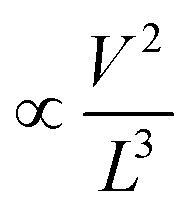 , where L is the channel length. Fig. 8c shows the I–V curves on a log–log scale where one can clearly see two distinct regions (A and B) for L below 10 μm. In region A, the current varies linearly with voltage whereas in region B, it shows quadratic dependence with voltage. This observation indicates the SCLC dominated carrier transport in MoS2 at high applied voltages. According to previous studies,43,49 the SCLC region becomes more pronounced at shorter channel lengths and the longitudinal electric field can be realized at relatively low voltages with channel lengths of a few hundred nm. In such devices, the trap states have been identified to have influence on the carrier transport mechanism. In our devices, we found that the SCLC conduction is more pronounced at high applied voltages when the channel length is <10 μm, consistent with previous findings. For larger channel lengths, the current transport is dominated by ohmic conduction even at high applied voltages, because the overall behaviour of the carrier is still dominated by free charge carrier density. Thus, it is clear that the onset of the SCLC conduction is greatly influenced by the channel length.
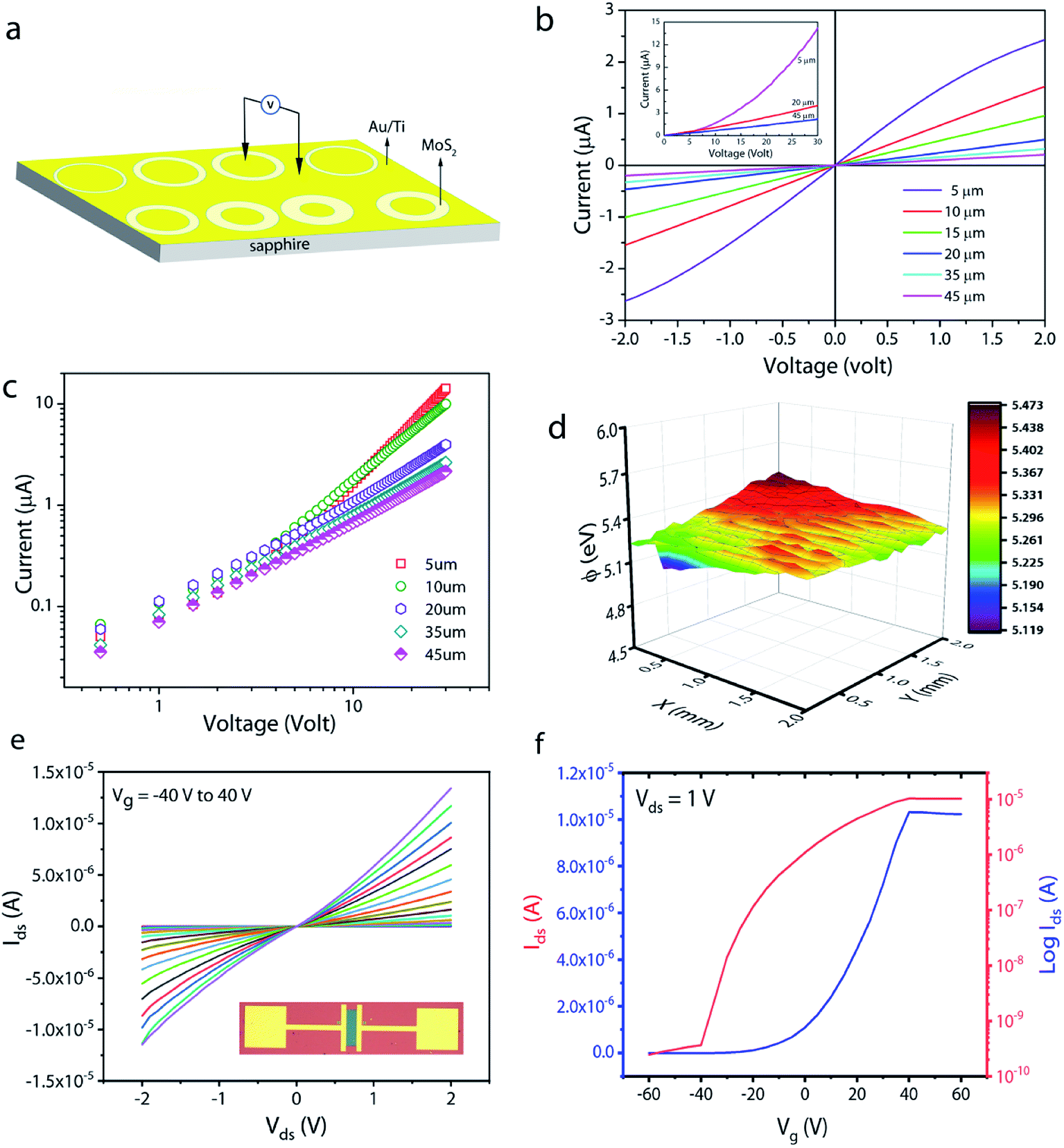 | ||
| Fig. 8 (a) Schematic of the two-terminal CTLM contact structure used for electrical measurements. I–V curves obtained for different channel lengths on a linear (b) and (c) log–log scale. (d) Surface work function mapping of MoS2 obtained using the scanning Kelvin probe system. (e) Ids–Vds curves for different gate voltages measured on a back-gated MoS2 FET device with a channel width of 20 μm. The inset is the optical image of a typical device. (f) Transfer characteristics of the same device at Vds = 1 volt. | ||
In order to further shed light on the electronic quality of the material, back-gated FETs were fabricated by transferring the MoS2 monolayer to heavily doped p++ Si capped with thermally grown 295 nm SiO2. Fig. 8e and f show the output and transfer curves of a representative device with a channel length and width of 20 μm and 350 μm, respectively. The Ids–Vds curves measured for different gate voltages are found to be linear at low (<1 volt) drain voltages, suggesting the ohmic nature of Ti contact, analogous to the CTLM results. Furthermore, the transfer characteristic curve in Fig. 8f shows typical n-type unipolar transport with anticipated transistor behaviour. The field-effect mobility is calculated using the expression 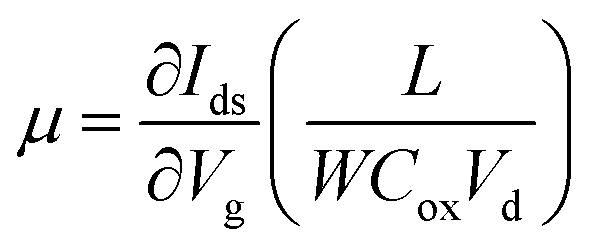 , where, Ids, Vd, and Vg denote drain current, drain voltage, and gate voltage, respectively, and L is the channel length, W is the channel width, and Cox is the dielectric capacitance per unit area (defined by Cox = ε0εr/d, where ε0 = 8.854 × 10⁻¹² F m−1, εr is dielectric constant of the oxide material (for SiO2, εr = 3.9) and d is the thickness of the dielectric film). The average room-temperature mobility is estimated to be about 1.2 cm2 V−1 s−1, which falls within the range of reported mobility values (0.1 to a few tens of cm2 V−1 s−1) for CVD-grown and exfoliated monolayer MoS2.4,23,25,26,50,51 However, the relatively low mobility observed in our devices compared to recent results reported in ref. 23 and 26 could be due to the wet-transfer process driven poor interface quality at MoS2/SiO2 and metal/MoS2 interfaces. While the theoretical upper bound of the room temperature mobility for monolayer MoS2 is predicted to reach a few thousands,52 the mobility values reported for practical devices are rather low due to intrinsic limitations including the large effective mass of the conduction band and significant phonon scattering, and other factors such as surface impurities, charge traps, intrinsic defects, etc. It is proven that sulfur vacancies can limit the carrier mobility by acting as scattering centres for charge carriers and active centres for molecular adsorption or chemical functionalization in the form of impurities.52,53 However, when oxygen occupies the vacancy sites and forms chemical bonding with Mo (Mo–O), it not only occupies the localized defect states but eventually removes the scattering centres. Based on the low temperature photoluminescence, it has been shown that the carrier mobility has a strong dependence on the IXb/IX0 ratio (IX0 and IXb denote the PL intensity of neutral excitons and bound excitons, respectively).33 It may be recalled once again that since in our samples the Xb peak was not present, the IXb/IX0 value is negligible and hence manifold improvement in charge carrier mobility is possible. We surmise that our MoS2 films can achieve high field-effect mobility by improving the transfer process and using the high-k dielectric environment. The relatively low (105 to 106) on/off ratio observed can be attributed to the high off-state current, because Mo–O bonding could likely lead to higher surface carrier concentration.54
Conclusions
In conclusion, large area continuous monolayer MoS2 films with high homogeneity were achieved by varying the substrate position in vapor phase chemical vapor deposition. The use of a simple mechanical barrier played a key role in controlling the Mo vapor concentration at the substrate position and in yielding homogeneous single crystal MoS2 with high optical and electronic quality. Optical microscopy and Raman spectroscopy allowed us to precisely determine the different secondary and intermediate phases and their position dependence in the grown MoS2. This study provides additional insight into the role of chemisorbed oxygen at sulfur vacancy sites in the photoluminescence characteristics and carrier mobility. The observation of strong photoluminescence suggests that the growth of single crystal continuous MoS2 using economical and non-toxic precursors demonstrated in this study would lead to the production of high-quality wafer-scale MoS2 films through further engineering of the reactor geometry. The method could also be extended to grow other transition metal dichalcogenides on a variety of substrates for the realization of electronic devices.Conflicts of interest
There are no conflicts to declare.Acknowledgements
SC would like to acknowledge the Science and Engineering Research Board (SERB), Department of Science and Technology, Govt. of India for the Research Grant (YSS/2015/000953). SC sincerely acknowledges SRM Institute of Science and Technology for the seed grant and generous support for the establishment of micro-Raman, UV-Vis-NIR spectrometer, and probe station facilities. Thanks are due to Dr S. Yuvaraj, SRM Institute of Science and Technology, for providing access to SKPM facility (established through research Grant No. ECR/2017/001218).Notes and references
- K. S. Novoselov, V. I. Fal, L. Colombo, P. R. Gellert, M. G. Schwab and K. Kim, Nature, 2012, 490, 192 CrossRef CAS PubMed.
- F. Withers, O. Del Pozo-Zamudio, A. Mishchenko, A. P. Rooney, A. Gholinia, K. Watanabe, T. Taniguchi, S. J. Haigh, A. K. Geim, A. I. Tartakovskii and K. S. Novoselov, Nat. Mater., 2015, 14, 301 CrossRef CAS PubMed.
- A. C. Ferrari, et al. , Nanoscale, 2015, 7, 4598 RSC.
- B. Radisavljevic, A. Radenovic, J. Brivio, V. Giacometti and A. Kis, Nat. Nanotechnol., 2011, 6, 147 CrossRef CAS PubMed.
- M. Chhowalla, H. S. Shin, G. Eda, L.-J. Li, K. P. Loh and H. Zhang, Nat. Chem., 2013, 5, 263 CrossRef PubMed.
- K. F. Mak, C. Lee, J. Hone, J. Shan and T. F. Heinz, Phys. Rev. Lett., 2010, 105, 136805 CrossRef PubMed.
- D. Xiao, G.-B. Liu, W. Feng, X. Xu and W. Yao, Phys. Rev. Lett., 2012, 108, 196802 CrossRef PubMed.
- Q. H. Wang, K. Kalantar-Zadeh, A. Kis, J. N. Coleman and M. S. Strano, Nat. Nanotechnol., 2012, 7, 699 CrossRef CAS PubMed.
- A. Splendiani, L. Sun, Y. Zhang, T. Li, J. Kim, C.-Y. Chim, G. Galli and F. Wang, Nano Lett., 2010, 10, 1271–1275 CrossRef CAS PubMed.
- J. N. Coleman, M. Lotya, A. O'Neill, S. D. Bergin, P. J. King, U. Khan, K. Young, A. Gaucher, S. De and R. J. Smith, Science, 2011, 331, 568 CrossRef CAS PubMed.
- J. W. Christopher, B. B. Goldberg and A. K. Swan, Sci. Rep., 2017, 7, 14062 CrossRef PubMed.
- D. Li, Z. Xiao, S. Mu, F. Wang, Y. Liu, J. Song, X. Huang, L. Jiang, J. Xiao and L. Liu, Nano Lett., 2018, 18, 2021–2032 CrossRef CAS PubMed.
- K. Kang, S. Xie, L. Huang, Y. Han, P. Y. Huang, K. F. Mak, C.-J. Kim, D. Muller and J. Park, Nature, 2015, 520, 656 CrossRef CAS PubMed.
- N. B. Shinde, B. Francis, M. S. Ramachandra Rao, B. D. Ryu, S. Chandramohan and S. K. Eswaran, APL Mater., 2019, 7, 81113 CrossRef.
- V. K. Kumar, S. Dhar, T. H. Choudhury, S. A. Shivashankar and S. Raghavan, Nanoscale, 2015, 7, 7802–7810 RSC.
- A. Gaur, D. Chiappe, D. Lin, D. Cott, I. Asselberghs, M. Heyns and I. Radu, 2D Mater., 2019, 6, 35035 CrossRef CAS.
- C.-C. Huang, F. Al-Saab, Y. Wang, J.-Y. Ou, J. C. Walker, S. Wang, B. Gholipour, R. E. Simpson and D. W. Hewak, Nanoscale, 2014, 6, 12792–12797 RSC.
- C. Chen, Z. Feng, Y. Feng, Y. Yue, C. Qin, D. Zhang and W. Feng, ACS Appl. Mater. Interfaces, 2016, 8, 19004–19011 CrossRef CAS PubMed.
- B. Chen, Q. Yu, Q. Yang, P. Bao, W. Zhang, L. Lou, W. Zhu and G. Wang, RSC Adv., 2016, 6, 50306–50314 RSC.
- A. Sharma, M. A. Verheijen, L. Wu, S. Karwal, V. Vandalon, H. C. M. Knoops, R. S. Sundaram, J. P. Hofmann, W. M. M. E. Kessels and A. A. Bol, Nanoscale, 2018, 10, 8615–8627 RSC.
- Y. Gao, Z. Liu, D.-M. Sun, L. Huang, L.-P. Ma, L.-C. Yin, T. Ma, Z. Zhang, X.-L. Ma and L.-M. Peng, Nat. Commun., 2015, 6, 8569 CrossRef CAS PubMed.
- Y. Gao, Y. Hong, L. Yin, Z. Wu, Z. Yang, M. Chen, Z. Liu, T. Ma, D. Sun and Z. Ni, Adv. Mater., 2017, 29, 1700990 CrossRef PubMed.
- P. Yang, X. Zou and Z. Zhang, et al. , Nat. Commun., 2018, 9, 979 CrossRef PubMed.
- J. V. Pondick, J. M. Woods, J. Xing, Y. Zhou and J. J. Cha, ACS Appl. Nano Mater., 2018, 1, 5655–5661 CrossRef CAS.
- Y.-F. Lim, K. Priyadarshi, F. Bussolotti, P. K. Gogoi, X. Cui, M. Yang, J. Pan, S. W. Tong, S. Wang and S. J. Pennycook, ACS Nano, 2018, 12, 1339–1349 CrossRef CAS PubMed.
- H. Yu, M. Liao, W. Zhao, G. Liu, X. J. Zhou, Z. Wei, X. Xu, K. Liu, Z. Hu and K. Deng, ACS Nano, 2017, 11, 12001–12007 CrossRef CAS PubMed.
- Z. Lin, Y. Zhao, C. Zhou, R. Zhong, X. Wang, Y. H. Tsang and Y. Chai, Sci. Rep., 2015, 5, 18596 CrossRef CAS PubMed.
- B. Li, S. Yang, N. Huo, Y. Li, J. Yang, R. Li, C. Fan and F. Lu, RSC Adv., 2014, 4, 26407–26412 RSC.
- R. Narro-García, N. Méndez, L. M. Apátiga, J. P. Flores-De los Ríos, C. G. Nava-Dino and R. Quintero-Torres, Int. J. Electrochem. Sci., 2017, 12, 3907–3915 CrossRef.
- C. Lee, H. Yan, L. E. Brus, T. F. Heinz, J. Hone and S. Ryu, ACS Nano, 2010, 4, 2695–2700 CrossRef CAS PubMed.
- H. Li, Q. Zhang, C. C. R. Yap, B. K. Tay, T. H. T. Edwin, A. Olivier and D. Baillargeat, Adv. Funct. Mater., 2012, 22, 1385–1390 CrossRef CAS.
- B. Chakraborty, H. S. S. R. Matte, A. K. Sood and C. N. R. Rao, J. Raman Spectrosc., 2013, 44, 92–96 CrossRef CAS.
- H. Nan, Z. Wu, J. Jiang, A. Zafar, Y. You and Z. Ni, J. Phys. D: Appl. Phys., 2017, 50, 154001 CrossRef.
- T. Korn, S. Heydrich, M. Hirmer, J. Schmutzler and C. Schuller, Appl. Phys. Lett., 2011, 99, 102109 CrossRef.
- X.-X. Zhang, Y. You, S. Y. F. Zhao and T. F. Heinz, Phys. Rev. Lett., 2015, 115, 257403 CrossRef PubMed.
- H. Nan, Z. Wang, W. Wang, Z. Liang, Y. Lu, Q. Chen, D. He, P. Tan, F. Miao and X. Wang, ACS Nano, 2014, 8, 5738–5745 CrossRef CAS PubMed.
- P. J. Ko, A. Abderrahmane, T. V. Thu, D. Ortega, T. Takamura and A. Sandhu, J. Nanosci. Nanotechnol., 2015, 15, 6843–6846 CrossRef CAS PubMed.
- Y. Yu, C. Li, Y. Liu, L. Su, Y. Zhang and L. Cao, Sci. Rep., 2013, 3, 1866 CrossRef PubMed.
- Y. Ho, C. Ma, T. Luong, L. Wei, T. Yen, W. Hsu, W. Chang, Y. Chu, Y. Tu and K. P. Pande, Phys. Status Solidi RRL, 2015, 9, 187–191 CrossRef CAS.
- G. Deokar, D. Vignaud, R. Arenal, P. Louette and J.-F. Colomer, Nanotechnol, 2016, 27, 75604 CrossRef CAS PubMed.
- X. Wang, Y. P. Zhang and Z. Q. Chen, Mater. Res. Express, 2016, 3, 65014 CrossRef.
- C.-R. Wu, X.-R. Chang, C.-H. Wu and S.-Y. Lin, Sci. Rep., 2017, 7, 42146 CrossRef CAS PubMed.
- S. Ghatak and A. Ghosh, Appl. Phys. Lett., 2013, 103, 122103 CrossRef.
- X. Xu, Z. Zhang, L. Qiu, J. Zhuang, L. Zhang, H. Wang, C. Liao, H. Song, R. Qiao and P. Gao, Nat. Nanotechnol., 2016, 11, 930 CrossRef CAS PubMed.
- I. Popov, G. Seifert and D. Tománek, Phys. Rev. Lett., 2012, 108, 156802 CrossRef PubMed.
- L. Britnell, R. M. Ribeiro, A. Eckmann, R. Jalil, B. D. Belle, A. Mishchenko, Y.-J. Kim, R. V. Gorbachev, T. Georgiou and S. V. Morozov, Science, 2013, 340, 1311–1314 CrossRef CAS PubMed.
- L. Feng, J. Su, D. Li and Z. Liu, Phys. Chem. Chem. Phys., 2015, 17, 6700–6704 RSC.
- S. McDonnell, C. Smyth, C. L. Hinkle and R. M. Wallace, ACS Appl. Mater. Interfaces, 2016, 8, 8289–8294 CrossRef CAS PubMed.
- M. R. Laskar, L. Ma, S. Kannappan, P. Sung Park, S. Krishnamoorthy, D. N. Nath, W. Lu, Y. Wu and S. Rajan, Appl. Phys. Lett., 2013, 102, 252108 CrossRef.
- M. Amani, M. L. Chin, A. G. Birdwell, T. P. O'Regan, S. Najmaei, Z. Liu, P. M. Ajayan, J. Lou and M. Dubey, Appl. Phys. Lett., 2013, 102, 193107 CrossRef.
- N. Huo, Y. Yang, Y.-N. Wu, X.-G. Zhang, S. T. Pantelides and G. Konstantatos, Nanoscale, 2018, 10, 15071–15077 RSC.
- X. Cui, G.-H. Lee and Y. D. Kim, et al. , Nat. Nanotechnol., 2015, 10, 534 CrossRef CAS PubMed.
- A. M. Van Der Zande, P. Y. Huang, D. A. Chenet, T. C. Berkelbach, Y. You, G.-H. Lee, T. F. Heinz, D. R. Reichman, D. A. Muller and J. C. Hone, Nat. Mater., 2013, 12, 554 CrossRef CAS PubMed.
- T. Zhang, Y. Wang, J. Xu, L. Chen, H. Zhu, Q. Sun, S. Ding and D. W. Zhang, 2D Mater., 2017, 5(1), 015028 CrossRef.
Footnote |
| † Electronic supplementary information (ESI) available. See DOI: 10.1039/d0na00524j |
| This journal is © The Royal Society of Chemistry 2020 |