
 Open Access Article
 This Open Access Article is licensed under a Creative Commons Attribution-Non Commercial 3.0 Unported Licence
Ammonium phosphomolybdate: a material for dielectric crossover and resistive switching performance†
Sarit K.
Ghosh
,
Venketa K.
Perla
,
Kaushik
Mallick
 and
Tarasankar
Pal
*
and
Tarasankar
Pal
*
Department of Chemical Sciences, University of Johannesburg, P.O. Box 524, Auckland Park 2006, Kingsway Campus, South Africa. E-mail: tpal@chem.iitkgp.ac.in
First published on 5th October 2020
Abstract
The yellow ammonium phosphomolybdate [(NH4)3PMo12O40] (YAPM) is a robust and elegant compound that has found innumerable field applications. Herein, we have shown that this inorganic polymer serves as a novel dielectric material and a compound for memory device fabrication. It displays changeable dielectric performance and ac conductivity under UV (∼365 nm) irradiation. Drastic lowering of the dielectric constant (ε′) was observed with the increase in dielectric loss factor, which was ascertained due to electron accumulation under UV exposure producing green APM (GAPM). The contributions of the Maxwell–Wagner polarization and the dipolar relaxation are correlated with the charge transfer and dielectric contribution of the material. Interestingly, the pressure-induced reduction of Mo(VI) to Mo(V) is reported for the first time and is similar to UV-exposed mixed-valence GAPM, which was corroborated by EPR spectra. In the ac signal, the crossover from quantum mechanical tunneling to hopping conduction is an adequate explanation for YAPM under UV irradiation. The fabricated device Au‖YAPM‖Au on a flexible paper substrate shows a resistive memory behavior that is modeled as a Schottky-type emission (SE) and Poole–Frenkel (PF) carrier transport for the OFF and ON states, respectively. The device exhibited a constant ON–OFF current ratio of 2 × 10² for YAPM. The OFF state endurance of the device (with 3 V pulses having 1 s time-period) under UV showed a steady increment current strength with time. After 100 s of UV exposure, the Au‖YAPM‖Au device became Au‖GAPM‖Au, and the conductivity completely shifted to a stable ON-state (at 300 s).
Introduction
Heteropolyacids (HPA) and related compounds have achieved worldwide importance because of their unique features of inherent acidity and oxidizing properties.1–4 Both features can be effectively used in many industrial applications and innovation in interdisciplinary research.5,6 Ammonium phosphomolybdate (APM) was the first polyoxometalate (POM) discovered almost two-centuries ago by Berzelius (1826) and was used as a reducing agent.7 The heteropolyoxometalates bear the Keggin-based anion [PMo12O40]3− and the substituents may be one or more frameworks of MO6 (M = Mo, W, V, Nb) pseudo-octahedra.8 The backbone of the [PMo12O40]3− anion consists of a central tetrahedral [PO4]−3 zone that provides strength to the molecule.3–9 Recently APM has been proved to be an attractive catalyst,10–12 a support material for drug delivery,13 performs biological activities,14 DNA synthesis and repair,14,15 sustain photochemical reaction,16–18 nanoparticle synthesis,19 cathode active material,20,21 and even electrochemical application.22 Many of these applications originated from the redox activity of the [PMo12O40]3− anion with a robust electron reservoir capability.23 It is worth mentioning that the HOMO–LUMO gap of the anion is 4.79 eV.3 Baker et al. proposed a model for electron infusion into the [PMo12O40]−3 anion that accounts for the participation of bridging oxygen atoms with reduced metal ion Mo(V) and nearest oxidized Mo(VI) partner.24 Also, the use of POMs as electron acceptors is well understood with organic donors.25 Thus, organic–inorganic hybrid binary oxide materials for non-volatile resistive switching for data/energy storage properties have evolved.26,27 The conductive polymer matrices accelerate the electron transfer process and even tune the conductivity through fully π-conjugated electron systems.21,28 Resistive switching from both MoO3 and MoS2-based devices have been reported, where the SET process originates from the migration of oxygen ions in the former case29 and charge modulation by photons occurs for the latter.30 Yamase proposed the mechanism of photo-reducible inter-valence charge transfer in POMs. The reaction was conducted on alkyl ammonium polyoxomolybdate, which showed that electrochromic coloration of the material occurred due to the trapping of d1 electrons at an appropriate metal site in MoO6 octahedra.18 The process involved the ligand to metal (O to Mo) charge transfer under UV irradiation. During the reduction process, the Mo(VI) site first evolved into an intermediate Mo(VI)–oxygen unsaturated ligand at the peripheral position. Therefore, the properties of photo-generated electrons in POMs engender photo-catalytic dye degradation,31 water purification,32 organic compound reduction33,34 and molecular spintronics.35,36 Nakamura et al. reported a dielectric anomaly in mixed valence POMs, which was associated with the dipolar relaxation.37 The study also reported that the fully oxidized Keggin structure did not exhibit any dielectric anomalies. A dye-functionalized APM has recently been reported as a unique reagent for molecular oxygen or nitrogen binding anions.38 However, to date there have been no straightforward reports on ammonium phosphomolybdate, a compound of UG and PG laboratories, through oxygen for ac conductivity, dielectric relaxation and switchable resistive memory device fabrication. Herein, for the first time, we have demonstrated the temperature and frequency-dependent conductivity, dielectric constant, vis-à-vis resistive switching memory effect.Experimental details
Laboratory synthesis of ammonium phosphomolybdate (APM) and device fabrication
All the chemicals and solvents used in this synthesis were analytical grade and were used without any further purification. In the synthesis process, sodium di-hydrogen phosphate NaH2PO4·2H2O (0.15 g) was dissolved in 20 mL of water, then added to a 40 mL solution of ammonium heptamolybdate (NH4)6Mo7O24·4H2O (2.3 g) and warmed at 80 °C. The solution was acidified with conc. HNO3 (4 mL) under stirring conditions and the final solution was kept for the next 60 minutes at the same temperature. The canary yellow precipitate of ammonium phosphomolybdate (YAPM) was filtered and then dried in a vacuum to furnish the product. The green ammonium phosphomolybdate (GAPM) was obtained from the YAPM after UV irradiation (λ ≈ 365 nm) for 6 hours. A flexible paper substrate was supported on a glass slide to provide the mechanical strength. A pair of gold electrodes were printed over the paper substrate and after that, the YAPM was deposited (thickness ∼ 10 μm) using the spin coating technique at 1200 rpm. Another pair of gold electrodes was deposited on the YAPM substrate to obtain the Au‖YAPM‖Au structure with an active area of 0.5 × 0.5 mm2, Fig. 9(a) (inset).Material characterization
The powder X-ray diffraction (XRD) patterns of the synthesized YAPM and GYAM were obtained using a Philips PANalytical X'pert diffractometer with Cu-Kα radiation. Infrared spectra were collected in the range from 400–1200 cm−1 using a Shimadzu IR Affinity-1 with a spectral resolution of 0.5 cm−1. Raman spectra were recorded using the 514.5 nm excitation of an argon ion laser source. Shifts in the Raman dispersion were observed via the single spectrograph stage of a Jobin-Yvon T64000 spectrometer. The EPR studies were done with a Bruker EMX spectrometer using an X-band microwave bridge (9.5 GHz) and a variable-temperature Bruker Unit ER 4111 VT working in the range of 170–500 K with good stabilization (±0.1 K). The experiments were carried out by using a low modulation field (3 Gauss) and 200 mW as the microwave power. These parameters are suitable for recording the EPR spectra without any distortion. Temperature- and frequency-dependent dielectric spectra were obtained for gold-coated pellets of 5 mm diameter and 0.2 mm thickness, using an HP 4284A LCR meter interfaced to a computer controlled EC1A environmental chamber in the temperature range from 20 °C to 40 °C and a step size of 5 °C. A high electric field versus polarization loops were collected using a modified Sawyer–Tower circuit (PolyK Tech.), where the samples were subjected to a triangular wave with a frequency of 100 Hz. All the electrodes were deposited using a physical vapor deposition technique (cathode sputter coater, EMSCOPE SC 500). For the fabrication of the thin film a MILMAN 4000A spin coater was used. The current–voltage (I–V) performance of the fabricated Au‖YAPM‖Au and Au‖GAPM‖Au devices were measured using a Keithley-2401 sourcemeter with the scan rate of 0.17 V s−1 and Icc (compliance current) of 1 mA throughout the I–V characterization.Results and discussion
Structural characterization
X-ray diffraction spectra of YAPM and GAPM are shown in Fig. 1. All the diffraction peaks are matched according to the cubic structure of space group Pn![[3 with combining macron]](https://www.rsc.org/images/entities/char_0033_0304.gif) m (ICDD: 000090412).
m (ICDD: 000090412).
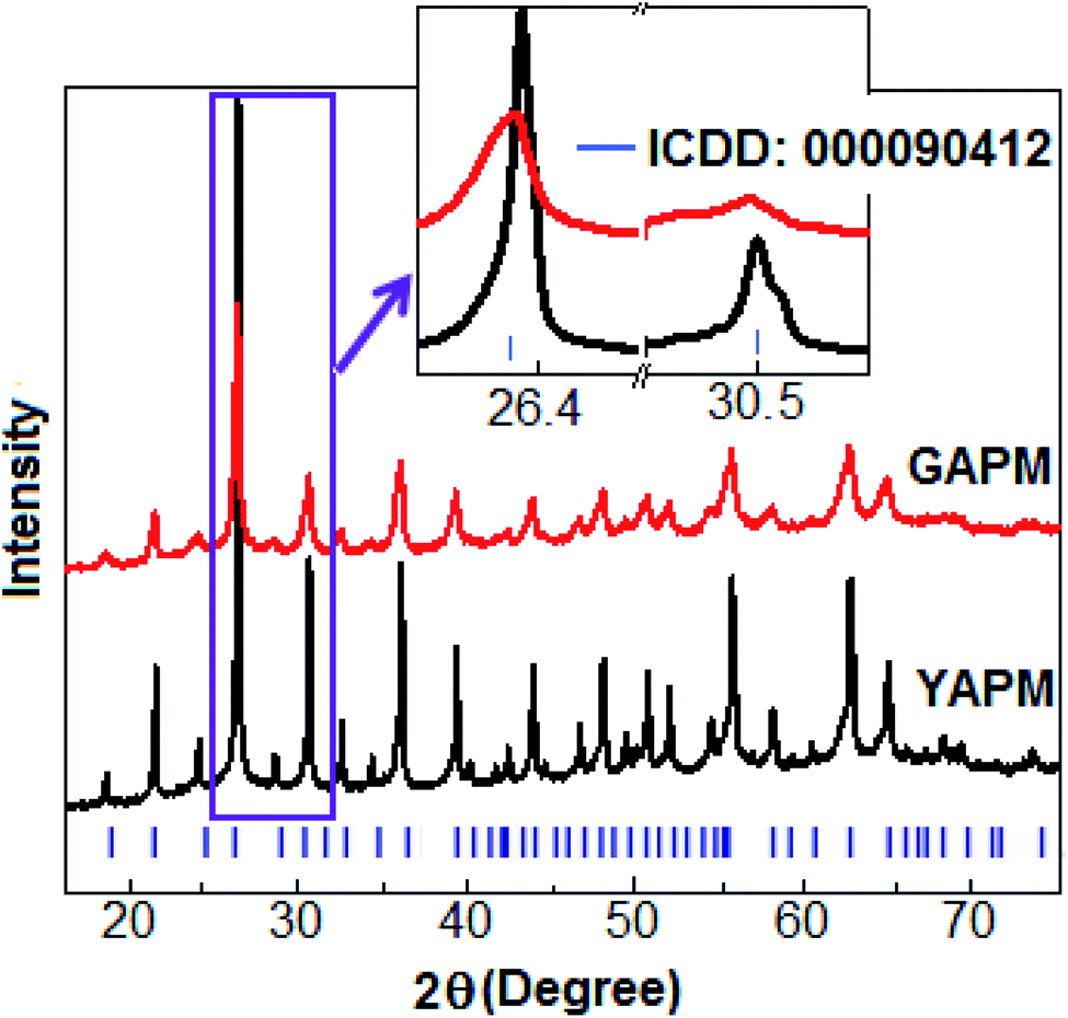 | ||
| Fig. 1 Room temperature X-ray diffraction patterns of YAPM (black line) and GAPM (red line) measured in the 2θ range from 18–75° and indexed according to the ICDD database (000090412), belonging to cubic symmetry. The inset figure highlights the shifting and broadening effect in the diffraction pattern. | ||
The diffraction peaks indicate that the YAPM and GAPM materials are in the single-phase without any trace of unreacted elements. The detailed peak profiles for two orientations of the (222) and (400) plane positions at 26.4° and 30.5°, respectively, are illustrated in the inset of Fig. 1. Rietveld refinement was performed for YAPM and GAPM materials and the values are (a = b = c) 11.54 Å and 11.59 Å, respectively, as shown in Fig. S1 (ESI†). A significant lattice strain developed in GAPM under UV irradiation caused the formation of oxygen defects or vacancies in the lattice, which resulted in the decrease in the intensity of the (222) Bragg diffraction peak, located at 26.4°. The strain was due to the variation in the atomic displacement, which caused a shifting of the diffraction peak towards the lower angle direction. The change in the intensity and peak position revealed the defect morphology and volume expansion in the unit cell structure. The transmission electron microscopy images of YAPM and GAPM are included in the ESI, Fig. S2.†
The comparison of the FTIR spectra of YAPM and GAPM materials are shown in the Fig. 2. The majority of the infared vibrational bands of the Keggin anion are found in the region between 1100–750 cm−1. Four characteristic vibrational peaks of Keggin anion positioned at 1061.1, 958.5, 862.6 and 763.8 cm−1 are observed, which are assigned to the stretching vibrations of P–Oa, Mo–Od, Mo–Oc–Mo and Mo–Ob–Mo modes for the polyhedral netwrok. The apperance of these vibrational modes in IR spectra indicates that the primary structure of Keggin unit of YAPM is totally restored even after prolong UV irradition. The weak intensity modes between 667.7–455.5 cm−1 is due to the other Mo–O bond vibration. The robost Keggin structure is found to remain unchanged, despite slightly reduced in intensity of the modes, which may be ascribed to the defect formation under the UV irridiation.
 | ||
| Fig. 2 FTIR spectra of YAPM and GAPM measured in the range from 400–1200 cm−1. | ||
The Raman spectra of YAPM and GAPM materials are shown in Fig. 3. The spectra show several intense Raman active modes in the wavenumber range from 200–1200 cm−1, which are assigned to typical vibrational modes involved with the Keggin structure (inset Fig. 3(a)). The major mode position at 280 cm−1 was assigned to the Mo–Oa vibration. Other modes positioned at 657 cm−1, 820 cm−1 and 988 cm−1 were assigned to Mo–Oc–Mo stretching, Mo–Ob–Mo asymmetric stretching and Mo–Od stretching vibrations, respectively, in the material.
 | ||
| Fig. 3 Raman spectra of ammonium phosphomolybdate measured in the range from 200–1200 cm−1 with and without UV irradiation. The inset diagrams show (a) the Keggin structure and (b) the variation of the heteropolymolybdate anions under UV irradiation. | ||
Under UV irradiation, the spectra show drastic changes in the vibrational modes. This could be induced by the charge transfer that occurred, causing an isomeric transformation. This structural change on the polyoxo-anions consists of the Mo3O13 groups located on the top of the overall polyhedron anion, inset Fig. 3(b). However, the broadening of the mode was observed under UV irradiation, which is due to the positional disorder or defect formation in the material. The bridge stretching characteristic was observed in the Keggin structure under UV irradiation with strong intensity in the Raman mode at the terminal oxygen atom (Od) and the central oxygen atom (Oa). The intensities of the Mo–Od and Mo–Oa modes were enhanced and shifted to new positions at 975 cm−1 and 230 cm−1, respectively. The red shift suggests interactions between (NH4+)3 and the terminal oxygen atoms of the [PMo12O40]3− anion.
Temperature-dependent (160–220 K) EPR spectra were obtained for the APM material after 6 hours of UV irradiation and the spectra are represented in Fig. 4. The spectrum obtained under UV radiation consists of a symmetrical line centered at g = 1.95; this value is assigned to the Mo ions in the valence state (+V). The inset figures show comparative spectra of YAPM and GAPM materials and their charge transfer mechanism. In the octahedral environment of Mo(VI), the UV radiation causes the charge transfer from oxygen to Mo ions. Hole-carrier stabilization occurs on the oxygen and Mo with valence state +V due to transferred electrons.18 The study revealed that the drastic increase in the intensity of the EPR signal happens by lowering the temperature, since the increase seems to follow the Curie law and may indicate the existence of diluted locations of Mo(V) ions in the structure. In other words, all the Mo ions were not stabilized by the valence state of +V, which revealed that a mixed valence state of +VI and +V, exists in the material. The change corroborates the as-obtained green color for the material.
 | ||
| Fig. 4 The main panel represents the temperature variation of the electron paramagnetic resonance (EPR) spectra of the GAPM material in an applied magnetic field. The inset shows the comparative spectra of YAPM and GAPM (at 220 K) and their possible charge transfer mechanisms under UV irradiation. | ||
Dielectric and conductivity performances
The temperature (20 °C to 40 °C, ΔT = 5 °C) and frequency (100 Hz to 1 MHz)-dependent dielectric constant (ε′) and dielectric loss tangent (tan![[thin space (1/6-em)]](https://www.rsc.org/images/entities/char_2009.gif) δ) properties of the YAPM and GAPM are illustrated in Fig. 5(a) and (b), respectively. The dielectric constant was more pronounced in the lower frequency region and gradually decreased with the increase in frequency. At the highest measured temperature (40 °C) the ε′ increased and attained a maximum value of 390 (at 100 Hz) with tanδ of 1.5 for YAPM materials. When the YAPM was irradiated under a UV source, drastic changes were observed in the dielectric constant and loss factor properties of material. The value of ε′ decreased to 200 and tanδ increased to a factor of 6.7 for GAPM, which is nearly 4.5 times higher than the YAPM material. The dispersion in the dielectric constant towards lower frequency (below 500 Hz) suggests the formation of the Maxwell–Wagner interfacial polarization.39,40 The Maxwell–Wagner polarization of the phosphomolybdate anion (PMo12O40)3− can occur via electron transfer process from the Mo(VI) to Mo(V) mixed valence complex. This can occur in one-electron or two-electron steps.41 This polarization causes an accumulation of electric charges at the interfacial region of the anion complex, which makes the system heterogeneous. Other mechanisms responsible for the dielectric properties of the YAPM are attributed to the reorientation of dipoles, originated from the distorting Mo–O framework. The relaxation of this dipolar contribution is manifested as the dielectric loss peak in the tanδ curve close to 106 Hz. This peak shifted to the lower frequency side with an additional featured hump (below 500 Hz), probably due to the relaxation of excess electrons generated in the material under UV radiation; these excess electrons led to increases in the dielectric loss with the decreasing frequency in the GAPM material. The variation of the dielectric constant depends on the electron mobility and it is expected that higher electron mobility leads to decreases in the dielectric constant value.
δ) properties of the YAPM and GAPM are illustrated in Fig. 5(a) and (b), respectively. The dielectric constant was more pronounced in the lower frequency region and gradually decreased with the increase in frequency. At the highest measured temperature (40 °C) the ε′ increased and attained a maximum value of 390 (at 100 Hz) with tanδ of 1.5 for YAPM materials. When the YAPM was irradiated under a UV source, drastic changes were observed in the dielectric constant and loss factor properties of material. The value of ε′ decreased to 200 and tanδ increased to a factor of 6.7 for GAPM, which is nearly 4.5 times higher than the YAPM material. The dispersion in the dielectric constant towards lower frequency (below 500 Hz) suggests the formation of the Maxwell–Wagner interfacial polarization.39,40 The Maxwell–Wagner polarization of the phosphomolybdate anion (PMo12O40)3− can occur via electron transfer process from the Mo(VI) to Mo(V) mixed valence complex. This can occur in one-electron or two-electron steps.41 This polarization causes an accumulation of electric charges at the interfacial region of the anion complex, which makes the system heterogeneous. Other mechanisms responsible for the dielectric properties of the YAPM are attributed to the reorientation of dipoles, originated from the distorting Mo–O framework. The relaxation of this dipolar contribution is manifested as the dielectric loss peak in the tanδ curve close to 106 Hz. This peak shifted to the lower frequency side with an additional featured hump (below 500 Hz), probably due to the relaxation of excess electrons generated in the material under UV radiation; these excess electrons led to increases in the dielectric loss with the decreasing frequency in the GAPM material. The variation of the dielectric constant depends on the electron mobility and it is expected that higher electron mobility leads to decreases in the dielectric constant value.
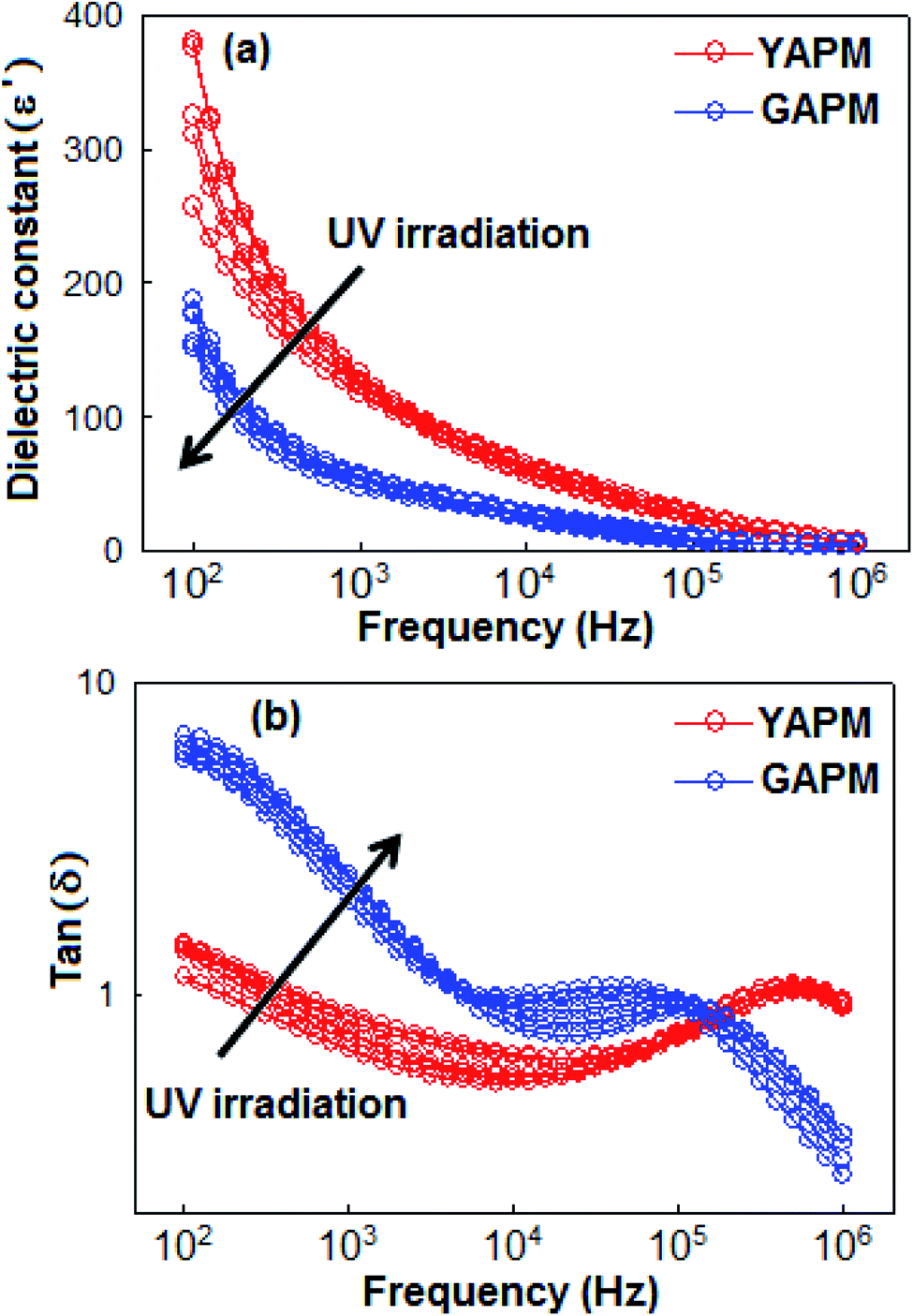 | ||
| Fig. 5 Frequency-dependent (a) dielectric constant (ε′) and (b) dielectric loss tangent (tanδ) curves of YAPM and GAPM materials measured at different temperatures (20 °C to 40 °C). | ||
For comparison, the dielectric properties of acidic phosphomolybdate H3[PMo12O40] (HPM) are plotted in Fig. S3 (ESI†). The higher value of the dielectric constant of the APM as compared to the HPM material is due to the pronounced covalence leading to larger size and higher polarization. One observation common to both APM and HPM is the color change (yellow to green). Upon the application of external pressure, HPM was observed to change its color to deep green in comparison to the APM, as shown in Fig. S4 (ESI†). This has a reference to an earlier observation.42 This may be due to the ratio of the two compounds, i.e., APM and HPM (size ratio [H+][PM] < [NH4+][PM]). This follows the pronounced covalence in the APM structure and its robustness. The dielectric relaxation was further studied in terms of modulus spectroscopy.
Fig. 6 represents the real (M′) and imaginary (M′′) parts of the modulus spectra of YAPM (a and b) and GAPM (c and d) materials at two temperature conditions (20 °C and 40 °C). The relaxation process was characterized by the peak position of the M′′ curves. No peak was observed for the YAPM material in the modulus spectra, and for GAPM material, it showed two relaxation anomalies in the M′′ curves. It has been established that the mixed valence state of the Keggin structure is responsible for dielectric anomalies.37 For the GAPM material, the origin of the weak relaxation hump between 103 to 104 Hz is due to the intermolecular charge transfer of the mixed valence of the Mo(VI) and Mo(V) states, whereas the other relaxation peaks above 105 Hz are due to the dipolar relaxation of the distorted Mo–O lattice. The maximum of the M′′ peaks shifted towards the higher frequency side with increasing temperature, which indicated the thermally activated dipolar relaxation. The region where the peak occurs indicates the transition from long-range to short-range mobility of the carriers with increases in frequency. This type of behavior indicates the existence of the temperature-dependent hopping mechanism for the charge conduction process. In addition, the broadening of the M′′ peaks with the rise in temperature shows the broadening of the relaxation time in the GAPM material.
 | ||
| Fig. 6 Real (M′) and imaginary (M′′) parts of the modulus spectra of YAPM (a and b) and GAPM (c and d) materials measured at two different temperatures (20 °C and 40 °C). | ||
These relaxation peaks were further confirmed by (M′′) versus (M′) Nyquist plots as shown in Fig. 7. The low-frequency semi-circular arc represents the interfacial relaxation process and the larger semicircular arc is attributed to the relaxation of the dipolar reorientation. The prominent semicircular arc for the GAPM material indicates that the excess charge carriers were generated due to the valence fluctuation of the Mo(VI)/Mo(V) state inside the anionic complex. This behavior is in accordance with the dielectric loss tangent curves of the materials.
 | ||
| Fig. 7 Nyqusit plot (M′ versus M′′) of (a) YAPM and (b) GAPM at two different temperature conditions. The arrow indicates the direction of decreasing frequency in the plot. | ||
Fig. 8 shows the ac conduction of YAPM and GAPM materials measured in different temperature and frequency regions. From the figure, it was observed that the ac conductivity increased with increasing temperature and frequency. The ac conductivity curve of GAPM shows three different conductivity regions, denoted as region I, region II and region III. Towards lower frequencies in region I, the plateau-like frequency-independent feature (100 Hz to 103 Hz) indicates the dc part of the conductivity. This behavior revealed that the large number of electron carriers contribute to the conductivity process in the GAPM material. On the other hand the YAPM material strongly follows the ac signal and the conductivity increases with frequency. The ac conductivity for both the materials followed a universal power relation, σac = σdc + A(T)ωS, where σdc is the frequency-independent dc part of the conductivity, A is the temperature-dependent factor that determines the strength of the polarizability, ‘s’ is the slope of the frequency-dependent parameter that varies from 0 to 1, which predicts the various types of conduction mechanism.43,44 The parameter ‘s’ is extracted by linear fitting using the above relation for separate regions (II and III) for GAPM, and the values are plotted (for selected temperatures) in the inset Fig. 8(a). It was observed that the ‘s’ parameter value increased slightly in region II (S1), whereas, in region III (S2), the value decreased sharply with temperature; the trends predict the conduction mechanism of the material (inset Fig. 8b). Various types of models have been proposed to understand the ‘s’ parameter, such as the quantum mechanical tunneling (QMT),45 correlated barrier hopping (CBH),46,47 overlapping large polaron tunneling (OLPT)48 and small polaron tunneling (SPT)49 model. According to the QMT model, the exponent ‘s’ is almost equal to 0.8 and increases with temperature. In the CBH model, ‘s’ usually decreases with increasing temperature and for the SPT model, ‘s’ increases with temperature. In the present GAPM material, the increasing trend for the ‘s’ in the low-frequency, region (II), indicates the tunneling effect of charge carriers, which crosses over to the hopping process in region (III) with increasing temperature. For YAPM, the overall conduction process is dominated by the quantum mechanical tunneling mechanism and the value of ‘s’ (0.72–0.75) increased slightly with temperature.
 | ||
| Fig. 8 AC conductivity of YAPM and GAPM measured at different temperatures from 20 °C to 40 °C (ΔT = 5 °C) and plotted on a log–log scale. Inset (a) shows the ac conductivity curves of GAPM at selected temperatures (20 °C and 40 °C) and the fitted (red line) according the universal power relation. Inset (b) represents the variation of S parameters for YAPM and GAPM materials versus temperature. | ||
Resistive memory and device fabrication
The current–voltage (I–V) characteristics of the device (Au‖YAPM‖Au) for the voltage sweep from 0 to +5, from +5 to −5 and from −5 to +5 V are illustrated in Fig. 9. Initially, the device achieved a high conduction state during the voltage sweep from 0 to +5 V. For the voltage sweep from −5 to +5 V, the device exhibited a SET process (switching from the low-conducting state to the high-conducting state) at 3.5 V, and a RESET process (back from the high-conducting state to the low-conducting state) occurred at 2.1 V for the voltage sweep from +5 to −5 V. A linear I–V plot is documented in Fig. S5 (ESI†). | ||
| Fig. 9 The current–voltage performance of the fabricated Au‖YAPM‖Au device plotted on a semi-log scale. Inset (a) is the schematic diagram of the device architecture on a flexible paper substrate. (b) I–V pattern of the UV-irradiated (GAPM) Au‖YAPM‖Au device. | ||
Identical SET and RESET behaviors were also observed on the other side of the I–V curve (negative bias). The ON–OFF current ratio was achieved with a value of 2 × 10² at 3.0 V. On the other hand, no resistive switching event happened for the device fabricated with GAPM, Fig. 9 (inset b). The current–voltage behavior of the YAPM-based device was also tested under exposure to UV-irradiation. The device initially showed the current value of 50 pA and in the presence of UV exposure, a steady improvement in current was noticed for the period of 100 s and the high conductance state (1 μA) was retained (Fig. 10(a)).
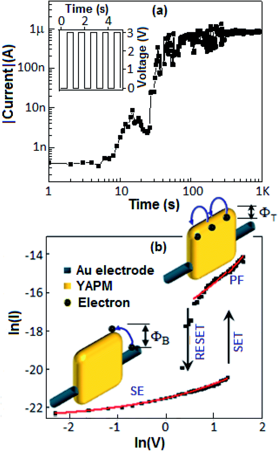 | ||
| Fig. 10 (a) The variation of the low conductance (OFF) state of the Au‖YAPM‖Au device with respect to time under UV irradiation; the inset shows the pulse train used to probe the conductance change in the device. (b) Schematic representation of the electron transport process of the device, modeled according to the Schottky and Poole–Frenkel mechanism for the low- and high-conductance state, respectively. | ||
The transport behavior of the device was followed via the ohmic mechanism for the initial voltage sweep from 0 to +5 V (Fig. S6, ESI†). The low-conductance (OFF) state, from 0 to +3.5 V, was fitted with the Schottky-emission type conduction mechanism, 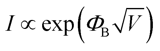 , where ΦB is the barrier height potential (∼0.52 eV) of the device extracted from fitting as shown in Fig. 10(b). The high-conductance (ON) state above 3.5 V was dominated by the Poole–Frenkel mechanism according to the relation
  , where, ΦT is the trap potential well in the high-conducting state of the material.
To determine the stability of the device, the endurance study was performed for several cycles. Prior to the endurance study, the device was subjected to a voltage sweep from 0 to +5 V (from +5 to 0 V) to impose a high-conductance state (low-conductance state) in the device. A pulse train of 103 with the amplitude of 3 V for a 0.1 s time period was employed to the device (Fig. 11, inset), where each pulse was separated by 0.1 s (50% duty cycle). The device exhibited stable ON- and OFF-states with an average ON–OFF current ratio of 2 × 10² for 103 cycles.
 | ||
| Fig. 11 The endurance analysis of the device was performed for 103 cycles. The inset shows the 3 V pulse train with 0.1 s time-period with an interval of 0.1 s (50% duty cycle) employed for the performance. | ||
Conclusion
The temperature and frequency-dependent dielectric relaxation, conductivity and resistive memory performance of ammonium phosphomolybdate (APM) are reported. The tailoring of the electrical properties of the materials when exposed to UV irradiation is correlated to the charge transfer between the Mo(VI) and Mo(V) states. Dielectric relaxation of the material followed the Maxwell–Wagner polarization effect and the dipolar relaxation of the distorted Mo–O structure, which was corroborated by EPR and modulus spectral analyses. Carrier migration in the ac signaled a changeover from quantum mechanical tunneling to the hopping conduction process in the UV-exposed green APM. Resistive switching behaviour was achieved in the fabricated Au‖YAPM‖Au device, which maintained a stable ON–OFF current ratio of 2 × 10². The OFF and ON states of the device were modeled according to the Schottky-type emission (SE) and Poole–Frenkel (PF) carrier conduction with an endurance test for 103 cycles. The color change was due to the Mo(VI) to Mo(V) conversion. This was ascertained from all the physical measurements. Therefore, the modification of the dielectric and memory device performances of YAPM material under UV irradiation has been reported for the first time and shows great potential for tuning capacitors and in memory device applications.Conflicts of interest
The authors declare no conflict of interest.Acknowledgements
This study was supported by the Faculty of Science and the Global Excellence and Stature (GES) program, University of Johannesburg. Also acknowledged Prof. A. Kassiba, Le Mans University (IMMM-CNRS) for measurement of EPR spectra for our samples.References
- M. T. Pope, Heteropoly and Isopoly Oxometalates, Springer-Verlag, 1983 Search PubMed.
- M. Misono, Catal. Rev.: Sci. Eng., 1987, 29, 269 CrossRef CAS.
- J. Hu and R. C. Burns, J. Catal., 2000, 375, 360–375 CrossRef.
- J. Hu and R. C. Burns, J. Mol. Struct., 2007, 152, 141–155 Search PubMed.
- H. N. Miras, J. Yan, D. Long and L. Cronin, Chem. Soc. Rev., 2012, 41, 7403–7430 RSC.
- Y. Song and R. Tsunashima, Chem. Soc. Rev., 2012, 41, 7384–7402 RSC.
- J. J. Berzelius, Ann. Phys., 1826, 82, 369–392 CrossRef.
- J. F. Keggin, Proc. R. Soc., 1934, 144, 5–100 Search PubMed.
- U. B. Mioč and Z. P. Nedić, in Encyclopedia of Membranes, ed. E. Drioli and L. Giorno, Springer Berlin Heidelberg, Berlin, Heidelberg, 2016, pp. 1077–1079 Search PubMed.
- K. N. Rao, C. Srilakshmi, K. M. Reddy, B. H. Babu, N. Lingaiah and P. S. S. Prasad, in Environmentally Benign Catalysts: For Clean Organic Reactions, ed. A. Patel, Springer Netherlands, Dordrecht, 2013, pp. 11–55 Search PubMed.
- S.-S. Wang and G.-Y. Yang, Chem. Rev., 2015, 115, 4893–4962 CrossRef CAS.
- H. Lv, Y. V. Geletii, C. Zhao, J. W. Vickers, G. Zhu, Z. Luo, J. Song, T. Lian, D. G. Musaev and C. L. Hill, Chem. Soc. Rev., 2012, 41, 7572–7589 RSC.
- J. T. Rhule, C. L. Hill, D. A. Judd and R. F. Schinazi, Chem. Rev., 1998, 98, 327–358 CrossRef CAS.
- W. E. G. Müller, H. C. Schröder and X. Wang, Chem. Rev., 2019, 119, 12337–12374 CrossRef.
- W. E. G. Mu, S. Wang, M. Neufurth, M. Kokkinopoulou, Q. Feng and H. C. Schro, J. Cell Sci., 2017, 130, 2747–2756 CrossRef.
- M. Basu, S. Sarkar, S. Pande, S. Jana, A. K. Sinha, S. Sarkar, M. Pradhan, A. Pal and T. Pal, Chem. Commun., 2009, 46, 7191–7193 RSC.
- C.-G. Lin, W. Chen and Y.-F. Song, in Polyoxometalate-Based Assemblies and Functional Materials, ed. Y.-F. Song, Springer International Publishing, Cham, 2018, pp. 49–63 Search PubMed.
- T. Yamase, Chem. Rev., 1998, 98, 307–326 CrossRef CAS.
- A. Troupis and A. Hiskia, Angew. Chem., Int. Ed., 2002, 41, 1911–1914 CrossRef CAS.
- H. Yoshikawa and K. Awaga, J. Am. Chem. Soc., 2012, 134, 4918–4924 CrossRef.
- Y. Ji, L. Huang, J. Hu, C. Streb and Y. Song, Energy Environ. Sci., 2015, 8, 776–789 RSC.
- W. Liu, X.-L. Wang and Y.-Q. Lan, in Polyoxometalate-Based Assemblies and Functional Materials, ed. Y.-F. Song, Springer International Publishing, Cham, 2018, pp. 89–119 Search PubMed.
- B. Botar, A. Ellern, R. Hermann and P. Kögerler, Angew. Chem., Int. Ed., 2009, 48, 9080–9083 CrossRef CAS.
- L. C. W. Baker and D. C. Glick, Chem. Rev., 1998, 98, 3–50 CrossRef CAS.
- P. Le Maguere, S. M. Hubig, S. V. Lindeman, P. Veya and J. K. Kochi, J. Am. Chem. Soc., 2000, 122, 10073–10082 CrossRef.
- C. Tan, Z. Liu and H. Zhang, Chem. Soc. Rev., 2015, 44, 2615–2628 RSC.
- T. W. Kim, Y. Yang, F. Li and W. L. Kwan, NPG Asia Mater., 2012, 4, e18 CrossRef.
- S. Herrmann, C. Richie and C. Streb, Dalton Trans., 2015, 44, 7092–7104 RSC.
- J. Fatheema, T. Shahid, M. Mohammad, A. Islam, F. Malik, D. Akinwande and S. Rizwan, RSC Adv., 2020, 10, 19337–19345 RSC.
- W. Wang, G. Panin, X. Fu, L. Zhang, P. Ilanchezhiyan, V. Pelenovich, D. Fu and T. Kang, Sci. Rep., 2016, 6, 31224 CrossRef CAS.
- J. M. Chem, A. Dolbecq, P. Mialane and L. Nadjo, J. Mater. Chem., 2012, 22, 24509–24521 RSC.
- B. Yang, J. J. Pignatello, D. Qu and B. Xing, J. Phys. Chem. A, 2015, 119, 1055–1065 CrossRef CAS.
- K. Yu, B. Wan, Y. Yu, L. Wang, Z. Su, C. Wang, C. Wang and B.-B. Zhou, Inorg. Chem., 2013, 52, 485–498 CrossRef CAS.
- K. Yu, B.-B. Zhou, Y. Yu, Z.-H. Su, H. Wang, C. Wang and C. Wang, Dalton Trans., 2012, 41, 10014–10020 RSC.
- J. Lehmann, A. Gaita-Ari
![[n with combining macron]](https://www.rsc.org/images/entities/char_006e_0304.gif) o, E. Coronado and D. Loss, Nat. Nanotechnol., 2007, 2, 312–317 CrossRef CAS.
o, E. Coronado and D. Loss, Nat. Nanotechnol., 2007, 2, 312–317 CrossRef CAS. - J. M. Clemente-Juan, E. Coronado and A. Gaita-Ariño, Chem. Soc. Rev., 2012, 41, 7464–7478 RSC.
- I. Nakamura, R. Tsunashima, S. Nishihara, K. Inouebc and T. Akutagawa, Chem. Commun., 2017, 53, 6824 RSC.
- A. K. Sasmal, A. K. Sinha, K. Mallick and T. Pal, Catal. Today, 2020, 348, 230–235 CrossRef CAS.
- L. Zhu, J. Phys. Chem. Lett., 2014, 5, 3677–3687 CrossRef CAS.
- C. Gaoru, X. Wang, J. Lin, W. Yang, D. Li, W. Ding and H. Li, J. Phys. Chem. C, 2017, 121, 15028–15035 CrossRef.
- N. N. Greenwood and A. Earnshaw, Chemistry of the Elements, Elsevier, 2nd edn, 1997, pp. 1–1341 Search PubMed.
- K. J. Rao and G. Parthasarathy, Phys. Chem. Glasses, 1985, 26, 101–104 CAS.
- Y. Ben Taher, A. Oueslati, N. K. Maaloul, K. Khirouni and M. Gargouri, Appl. Phys. A, 2015, 120, 1537–1543 CrossRef CAS.
- S. Nasri, A. L. Ben Hafsia, M. Tabelloutd and M. Megdichea, RSC Adv., 2016, 6, 76659–76665 RSC.
- S. S. Montasser and M. F. Mostafa, Z. Naturforsch. A, 2000, 55, 945–956 Search PubMed.
- K. Tsuji, H. Han, S. Guillemet-Fritsch and C. A. Randall, Phys. Chem. Chem. Phys., 2013, 1, 1–3 Search PubMed.
- S. Hajlaoui, I. Chaabane and K. Guidara, RSC Adv., 2016, 5, 91649–91657 RSC.
- Y. Ben Taher, A. Oueslati and M. Gargouri, Ionics, 2015, 21, 1321–1332 CrossRef CAS.
- E. W. Lim and R. Ismail, Electronics, 2015, 4, 586–613 CrossRef CAS.
Footnote |
| † Electronic supplementary information (ESI) available. See DOI: 10.1039/d0na00481b |
| This journal is © The Royal Society of Chemistry 2020 |