DOI:
10.1039/D0NA00442A
(Paper)
Nanoscale Adv., 2020,
2, 3582-3587
Design and circuit simulation of nanoscale vacuum channel transistors
Received
29th May 2020
, Accepted 27th June 2020
First published on 29th June 2020
Abstract
Nanoscale vacuum channel transistors (NVCTs) are promising candidates in electronics due to their high frequency, fast response and high reliability, and have attracted considerable attention for structural design and optimization. However, conventional modeling for vacuum devices tends to focus on the work function or electric field distribution for an individual structure. Therefore, it is desirable for a new simulation method to explore the function circuits of NVCTs, e.g. high-speed logic circuits. In this study, a complete simulation of the fabrication, structure design and circuit simulation of NVCTs is demonstrated. First, the fabrication process was designed to be compatible with current semiconductor technology. Then, the “fabricated” structure was directly employed to investigate the influence of the structure parameters on the electrical performance. Furthermore, we explore the possibility of implementing an invert circuit with a single optimal NVCT. To the best of our knowledge, this is the first demonstration of a vacuum-state invertor with a circuit-simulation module in which NVCT functions as a conventional triode or FET. These simulation results illustrate the feasibility of integrating NVCTs into functional circuits and provide a theoretical method for future on-chip vacuum transistors applied in logic or radio-frequency (RF) devices.
Introduction
As one of the core components in electronic technology, vacuum electronics have greatly promoted the development of modern society and have an irreplaceable function in a broad range of fields, e.g. aerospace, communications and medical.1–3 However, traditional vacuum devices are limited by the difficulty of high integration, while human demands for electronic devices have inevitably led to miniaturization nowadays. As vacuum devices have an irreplaceable function in some specific areas, there is an urgent need to develop a new generation of nanoscale vacuum electronic devices with high integration and efficiency.4
Recently, an alternative approach that involves combining a nanoscale vacuum channel with current semiconductor processing was proposed to realize novel vacuum nano-devices with high frequency, fast response and high reliability.4–7 Han et al. at NASA first proposed a planar nanoscale vacuum channel transistor (NVCT) with a structure similar to that of the conventional field effect transistor (FET), in which the carrier transport follows the tunneling mechanism rather than the drift-diffusion process.4 In 2017, they further proposed an NVCT with a gate-all-around (GAA) structure, performing at a low voltage (<5 V) with a high drive current (>3 μA). More importantly, the NVCT has proven to be robust against high temperatures (200 °C) and ionizing radiation (1 krad proton and 100 krad γ radiation).6,7 Moreover, the sub-100 nm vacuum channel can effectively reduce collisions or scattering during carrier transport, demonstrating its intrinsic advantages of low power consumption and fast response.5,8 In addition, by optimizing electrode materials such as metal, graphene or other low-dimensional materials, NVCTs indicate the potential for on-chip vacuum devices with high integration.9–13
The reported work4–13 reflect the research enthusiasm for NVCTs and show that vacuum nanoelectronics represent a possible method to obtain solid-state devices beyond the limits predicted by Moore's law. However, the conventional modeling and simulation methods for vacuum devices may not be suitable for new device structures such as NVCTs. For instance, the conventional modeling methods tend to focus on the work function, the trajectories of electrons or electric field distribution for an individual structure.14–17 On the other hand, the critical factors for modeling integrated devices depend on the overall electrical characteristics of function circuits, and few related simulation results have been achieved as yet. This gap could seriously hinder the transition of NVCTs from vacuum nano-structures to practical applications. Therefore, it is desirable to develop a novel simulation method to explore NVCTs in terms of device structures, and more importantly, function circuits such as those with high-speed logic applications.18
In this study, the semiconductor design software Silvaco TCAD was applied for establishing a physical model of NVCTs and studying the influence of the structural parameters on the electrical performance.19,20 We also explore the possibility of implementing logic circuits with a single NVCT. First, the fabrication process for NVCTs is designed in the fabrication-process module to be compatible with current semiconductor technology. In addition, we directly employ the “fabricated” structure in the device-simulation module. By applying bias and gate voltages, the influence of the structural parameters on the electrical performance is explored, such as the vacuum channel length and the thickness of the insulator layer. Moreover, we present the first demonstration of a vacuum-state inverter in the circuit-simulation module, in which the NVCTs function as the conventional triode or FET. The temporal response characteristics are further investigated. The reported results include simulation methods with a focus on the fabrication process, structure design and function circuit, thus providing an important theoretical basis for the future development of on-chip vacuum devices.
Results and discussion
Fabrication process
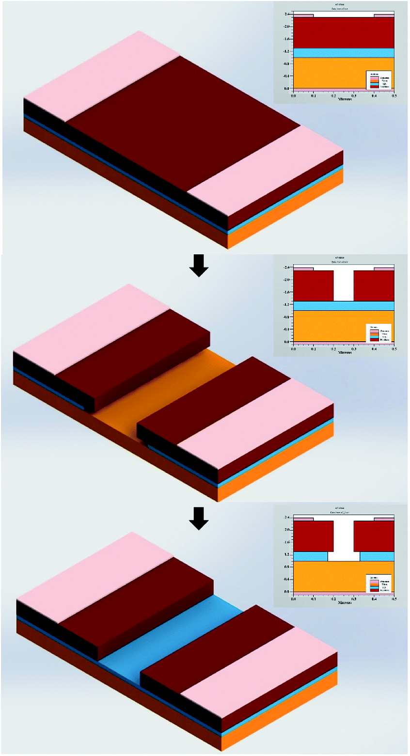
Fig. 1 shows a schematic of the fabrication process for an NVCT in the fabrication-process module, which can be applied directly with current semiconductor processing technology. First, silicon dioxide, polysilicon and aluminum are sequentially deposited on the silicon substrate, acting as the insulator layer, emitter/collector and electrode, respectively. The nanoscale vacuum channel can be achieved via electron beam lithography (EBL) or focus ion beam (FIB). Besides, the insulator layer contact with the carrier transport channel is always removed in conventional FETs, which not only reduces the surface conduction current but also effectively prevents the leakage current. Therefore, a chemical etching process is applied on the silicon dioxide between the vacuum channel and bottom gate. After the device structure is complete, the designed NVCT can be directly employed in the device simulation module, with subsequent electrical performance simulations.
 |
| | Fig. 1 Schematic of the fabrication process for NVCT. | |
Physical model
An appropriate physical model is required prior to the simulation of the device performance. It is well known that solid state devices conform to the drift-diffusion mechanism, while this principle is clearly not applicable for the carrier transport in a vacuum channel. Thus, the Fowler–Nordheim (F–N) tunneling model was utilized in the simulation, according to the theoretical model and experimental data in previous ref. 21 and 22. The F–N tunneling process is strongly dependent on the external electric field, which may cause the tunneling of electrons from the Fermi level of the emitters into the vacuum.23,24 The electric field distribution and emission current can be calculated using the theoretical formulas of the physical model. It is a part of the solutions to the equations and exhibits accurate properties for the NVCTs. The F–N equation is given as:| |  | (1) |
where J is the emission current density (A m−2), F is the electric field of the emitters (V m−1), e is the electron charge (C), h is the Planck's constant (Js), ϕ is the work function of the material (eV), m is the electron mass (kg), y is the parametric function of F with ϕ, and t(y) or v(y) is the approximate constant. Moreover, the F–N equation can be further simplified as| |  | (2) |
where β is the field enhancement factor and A = 1.54 × 10⁻⁶ and B = 6.83 × 10⁷ are constants. Substituting J = I/α and F = V × d into eqn (2), eqn (2) can be deduced as| |  | (3) |
| |  | (4) |
| |  | (5) |
where α is the effective emission area (m2), and d is the width of the vacuum channel (m). Taking the logarithmic transformation of eqn (3), eqn (6) is the commonly used F–N fitting equation that determines whether the tunneling process occurs.| |  | (6) |
As a result, the F–N tunneling model and the corresponding derivation formulas were introduced to enhance the accuracy of the following simulations, e.g. emission current and electric field distribution. On the other hand, the differences of the F–N model and the drift-diffusion mechanism lead to the distinctions between the electrical performances of NVCTs and FETs, and these distinctions directly affect the circuit simulations of NVCTs. Further discussions are included in the following sections.
Structural parameters
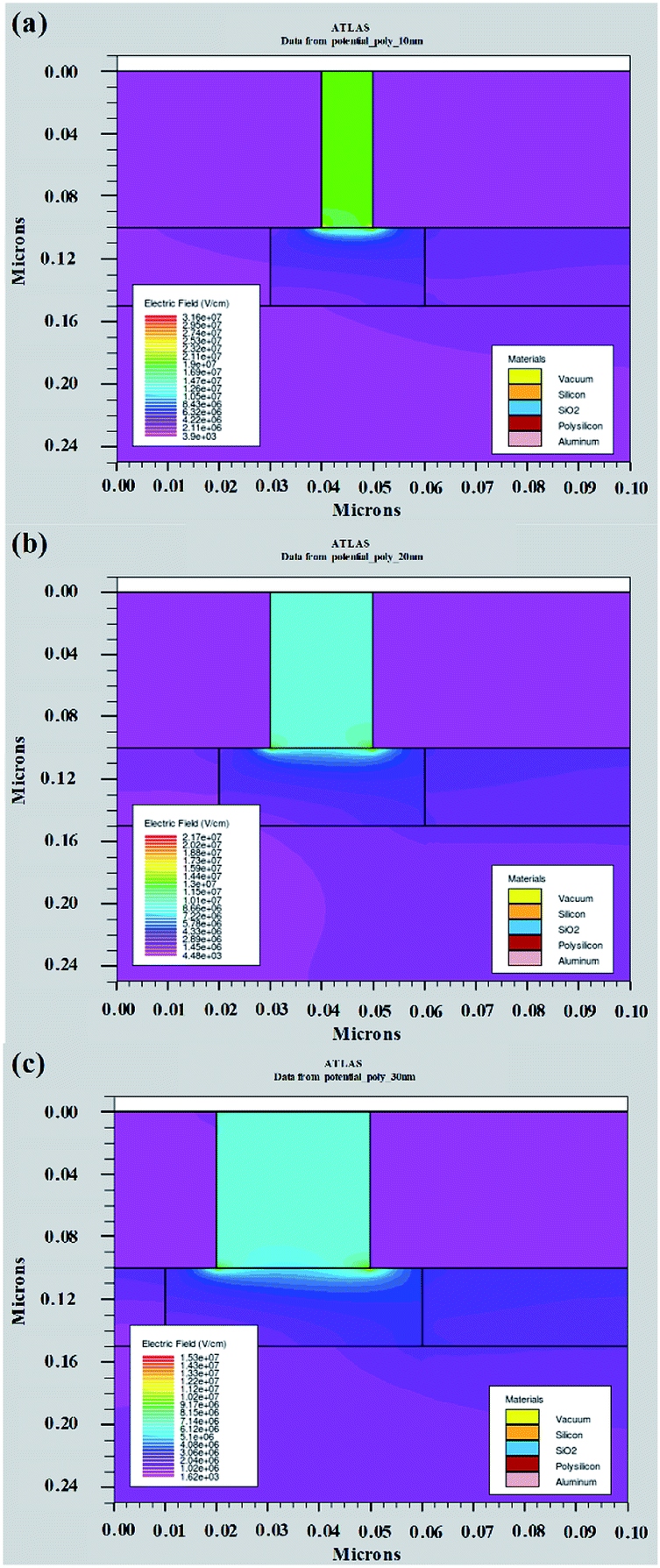
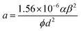
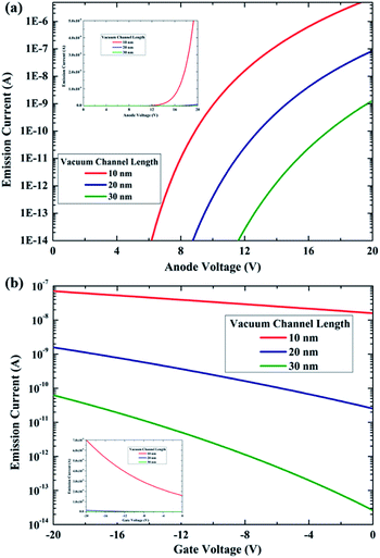
After establishing the physical model, the simulations of the electrical performance can be carried out with various structural and material parameters. In general, it is essential to divide the mesh appropriately in the vacuum channel or interface of different materials to improve the calculation accuracy. Here, we define the minimum grid accuracy as 0.1 nm, which meets the accuracy requirement. As for the numerical methods, the Newton method was chosen for the iterative calculations. To start with, we kept the emitter material (polysilicon) and the thickness of the insulator layer (150 nm) constant while altering the length of the nanoscale vacuum channel. Fig. 2 shows the electrical field intensity distribution in vacuum channels with various lengths. It is observed that the field intensity significantly improves as the channel length decreases from 30 nm to 10 nm, which may accordingly enhance the electrical properties of the NVCTs, e.g. emission current or turn-on voltage.
 |
| | Fig. 2 The electric field intensity distribution of nanoscale vacuum channels with various lengths, (a) 10 nm, (b) 20 nm and (c) 30 nm. | |
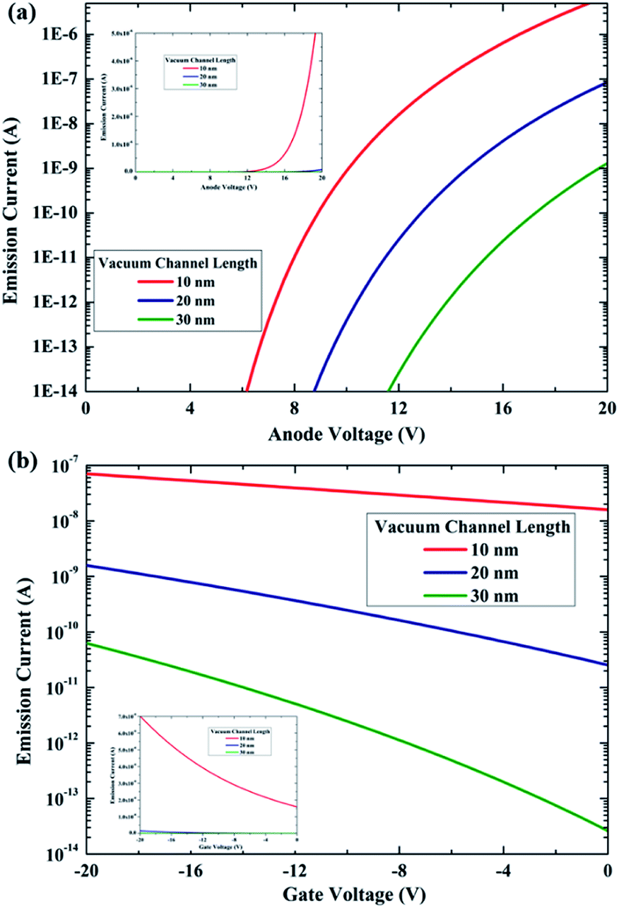
Moreover, all the emitter-to-vacuum and vacuum-to-collector interfaces should be divided into discrete segments based on the mesh, and the emission current is calculated using the F–N equations described above. The total emission current is then the sum of the currents from all the individual segments around the electrode boundary. Fig. 3 shows the output characteristic and transfer characteristic curves of nanoscale vacuum channels with various lengths (from 10 nm to 30 nm). Fig. 3(a) exhibits that the emission current increases exponentially with the increase in the anode voltage (inset), which is consistent with the F–N tunneling model and conventional field emission phenomena. We also note that the turn-on voltage of NVCTs increases with the increase in the channel length, which corresponds to the trend of the field intensity distributions in Fig. 2.
 |
| | Fig. 3 The (a) output characteristic and (b) transfer characteristic curves of nanoscale vacuum channels with various lengths in the logarithmic form. The insets show the I–V curves in the linear form. | |
Furthermore, a bias voltage was set on the bottom gate to modulate the emission current, and the transfer characteristic curves at a fixed anode voltage of 12 V are shown in Fig. 3(b). It is observed that NVCTs exhibit a conventional PMOS-like behavior, in which increasing the gate voltage in the forward direction suppresses the output current. This phenomenon coincides with the experimental results reported by Nirantar et al. that metal-based NVCTs turn off with the increase in gate voltage in a positive-bias operation.9 Besides, devices with a larger gap spacing possess better gate modulation and on/off current ratios, while the total emission current is relatively lower.
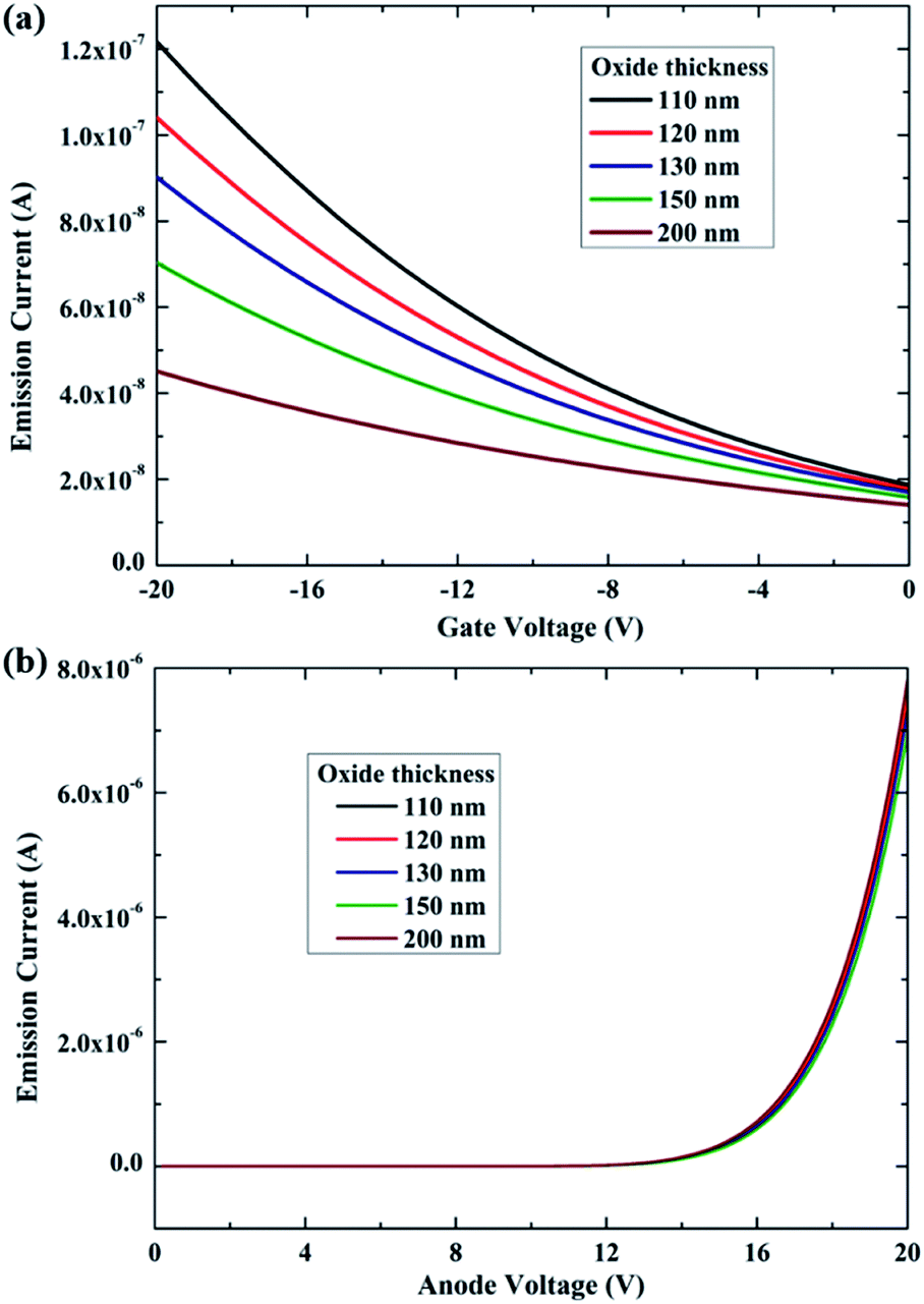
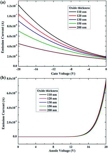
In addition, we further altered the thickness of the insulator layer to determine the capability of gate modulation with a constant nanoscale vacuum channel of 10 nm. It can be seen that the gate-control capability is remarkably enhanced as the thickness of the insulator layer decreases from 200 nm to 110 nm, as is shown in Fig. 4(a). The total emission current of NVCTs is almost constant and independent of the thickness (Fig. 4(b)). Meanwhile, the leakage current increases by two or three orders of magnitude with further reductions in the insulation thickness, showing an inevitable compromise between gate modulation and gate leakage, particularly for planar-type NVCTs with a bottom-gate structure. The electrical performance of NVCTs are limited by this so-called “trade-off” effect. On the one hand, the gate controllability of NVCTs can be effectively improved by compressing the thickness of the insulator layer. Nevertheless, excessively decreasing the insulating layer thickness leads to a large gate leakage current. As a result, for a practical device design, a comprehensive consideration is required to achieve a balance of the structural parameters, thereby obtaining optimal electrical performance.
 |
| | Fig. 4 The (a) transfer characteristic and (b) output characteristic curves of nanoscale vacuum channels with various oxide thicknesses in the linear form. | |
Inverter circuit simulation
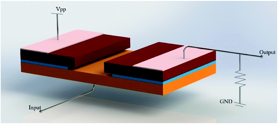
So far, discussions have focused on the fabrication process and structural design and not the simulations of the NVCT-based functional circuit. The latter is still an important part that recent research lacks. Therefore, we further adapted the optimized NVCT in the circuit-simulation module with a 10 nm vacuum channel, 110 nm-thickness insulator layer and poly-Si as an emitter/collector material. Since metal-based NVCTs exhibit a typical PMOS-type behavior, a simplified inverter circuit can be built based on a single transistor, as shown in Fig. 5. According to the output characteristic curves, the supply bias Vpp and external resistance are set as 10 V and 1 GΩ, respectively. On the other hand, the input signal is a square wave signal with a low level of 0 V and a high level of 5 V.
 |
| | Fig. 5 Schematic of the inverter circuit based on the proposed NVCT. | |
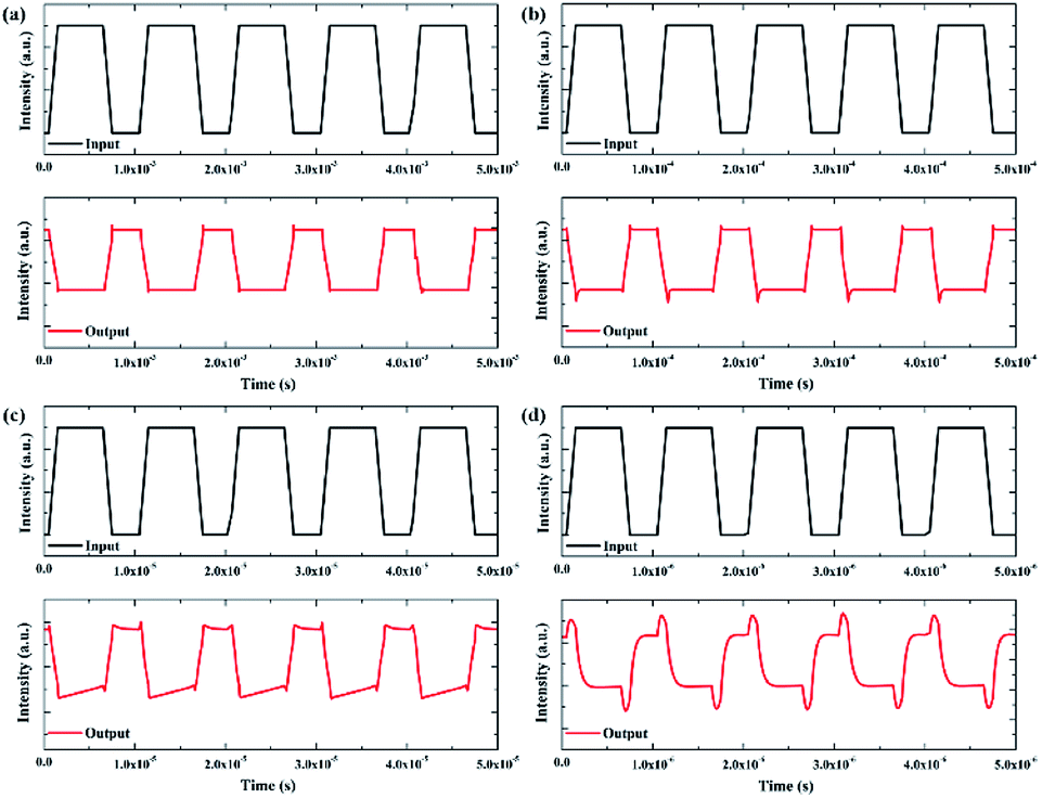
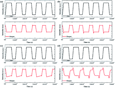
Fig. 6 shows the temporal response characteristics of the NVCT-based inverter with various input square waves of 100 μs, 10 μs, 100 μs and 100 ns. It can be seen that the simulated inverter circuit repeatedly exhibits a good inversion function as the input response time decreases. To our knowledge, these represent the first simulation results for a NVCT-based inverter. With various input signals, the rise/fall times of the inverter are shown in Table 1. Here, the rise/fall time is determined as the time it takes for the output voltage to increase from 10% (90%) to 90% (10%) upon a change in the input voltage. However, it is noted that the output invariably generates a “spike” or transient pulse signal when the direction of the electric field of the input signal reverses. This phenomenon becomes more distinct as the delay time of the input signal is reduced. We suppose that it may result from the capacitance between the bottom gate and the cathode/anode and is understood by the classic flat capacitor model.25 Regarding the NVCT as a plate capacitor, the reversal of the electric field direction would generate an instantaneous charge and discharge, thus leading to a transient pulse signal. When the input response time reaches 100 ns, the charging/discharging time of the capacitor cannot keep up with the reversal of the electric field. Therefore, the NVCT-based inverter functions before the capacitor is completely discharged, which also explains why the results in Fig. 6(d) differ from the others. Further decreasing the input response time would aggravate this phenomenon, affecting the operation of the inverter function.
 |
| | Fig. 6 Temporal response characteristics of an NVCT-based inverter with various square wave input signals of (a) 100 μs, (b) 10 μs, (c) 100 μs and (d) 100 ns. | |
Table 1 The corresponding rise/fall times with various input response times
| Input signal |
100 ns |
1 μs |
10 μs |
100 μs |
| Output rise time |
277.1 ns |
1.4 μs |
11.6 μs |
108.2 μs |
| Output fall time |
266.5 ns |
1.2 μs |
13.3 μs |
119.8 μs |
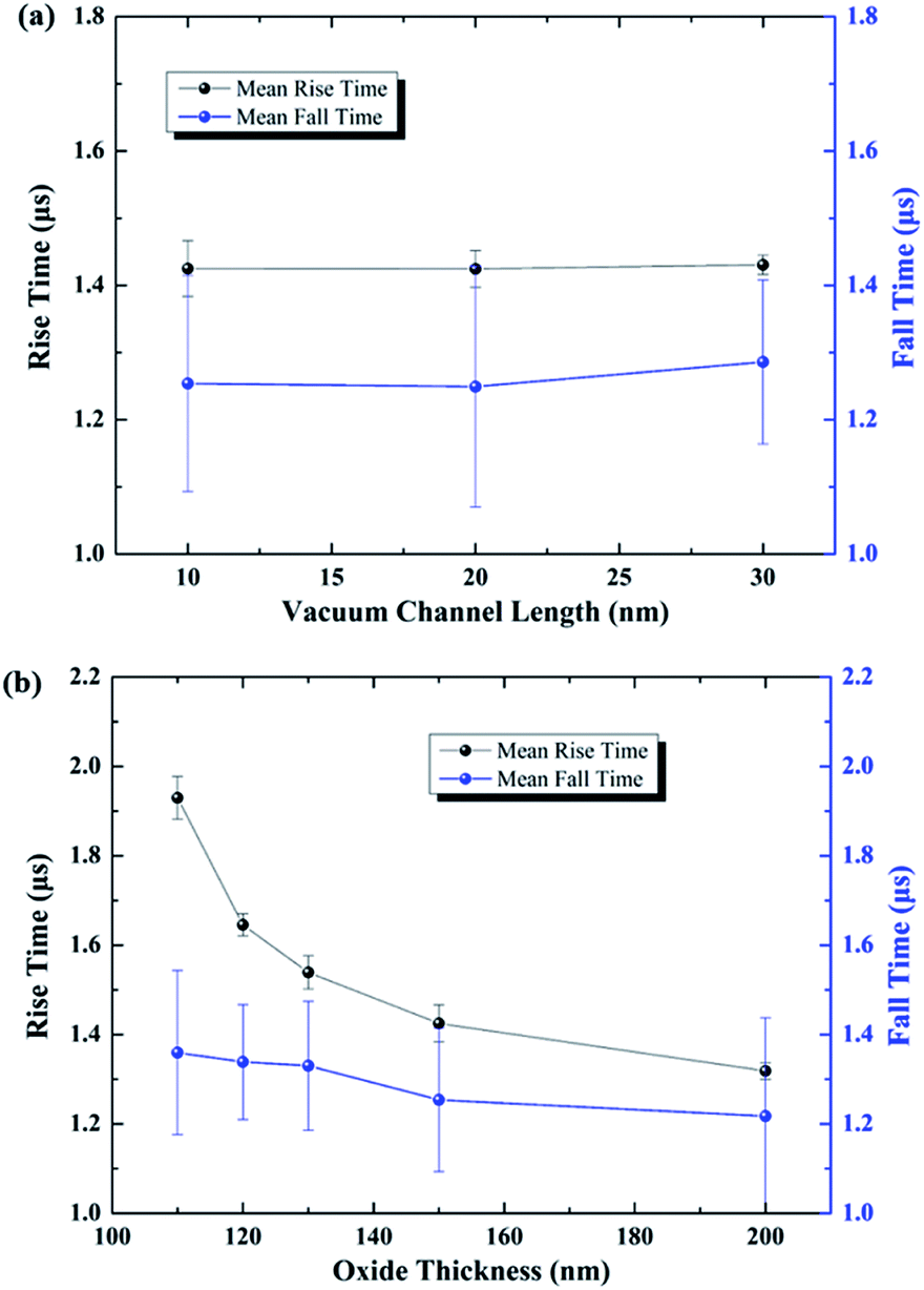
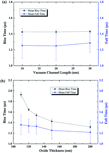
The temporal response characteristics of the proposed NVCT-based inverter with various vacuum channel lengths and oxide thicknesses are further demonstrated, as shown in Fig. 7(a) and (b). It is noted that the rise/fall time remains consistent with the increasing vacuum channel length. On the other hand, the response time characteristics show a distinct reduction as the thickness increases from 110 nm to 200 nm.
 |
| | Fig. 7 Simulation results of the temporal response of an NVCT-based inverter with various (a) vacuum channel lengths and (b) oxide thicknesses. | |
According to the classic flat capacitor model (C ∝ ε0εrS/d), the equivalent capacitance is related to the gap distance d from the bottom gate to the cathode/anode, which is in direct proportion to the insulator thickness. Meanwhile, the relative area S between the bottom gate and top electrodes basically remains unchanged in spite of the varying vacuum channel length (at a magnitude of 10 nm). As a result, the simulation results for the temporal response show agreement with the flat-capacitor model, which makes the above conclusion more convincing.
Besides, we found that the intensity of the output decay significantly compares with the input signal. The intensity is supposed to be related to the electrical characteristics of NVCTs. Conventional solid-state devices realize inverse function by voltage distribution. As the input signal rises from a low level to a high level, the solid-state transistor operates in the saturation region with the entire circuit remaining in a steady state. For NVCTs, on the other hand, the emission current conforms to the F–N tunneling mechanism, which increases exponentially with the anode voltage without a saturation region. One alternative approach is to set the divided voltage of the external resistance low enough that it cannot evidently influence the emission current. Thus, the output can operate in the steady state while leading to a significant reduction in the intensity of output signals. The above discussions illustrate that there still exist practical problems for the NVCT-based inverter, with the expectations of further improvements in the circuit design and optimization. For example, a filter circuit can be introduced to alleviate the charging/discharging phenomenon. Nonetheless, these simulation results explore the feasibility of integrating NVCTs into functional circuits, thus providing a theoretical method for future on-chip vacuum transistors applied in logic or radio-frequency (RF) devices.
Conclusions
In summary, this study comprehensively explores the modeling, structure design and circuit simulations of nanoscale vacuum channel transistors. First, the structural model of NVCT is established in the fabrication-process module. The as-prepared devices can be directly applied in the device-simulation module to carry out the following electrical performance investigation. In addition, we further altered and optimized the structural parameters, such as the length of the vacuum channel and insulator thickness. More importantly, we successfully realized an inverter circuit based on an optimal NVCT. To the best of our knowledge, it is the first demonstration of a vacuum-state inverter in the circuit-simulation module in which the NVCT functions as a conventional triode or field-effect transistor (FET). The simulation results in this paper are more focused on the performance of the transistors and external circuits than the electric field distributions or electron trajectory. Besides, the proposed device structure can be fabricated by standard semiconductor processes and may be viewed as an alternative approach for constructing NVCT-based circuits, thus providing an important theoretical and design basis for integrated on-chip vacuum devices.
Conflicts of interest
There are no conflicts to declare.
Acknowledgements
This work is financially supported by the National Natural Science Foundation of China (61904029, 61571124, 61971133), Key Laboratory Foundation Project (61428030305), the China Postdoctoral Science Foundation (2019M651646).
Notes and references
- R. S. Symons, IEEE Spectrum, 1998, 35, 52–63 Search PubMed.
- R. K. Parker, R. H. Abrams, B. G. Danly and B. Levush, IEEE Trans. Microwave Theory Tech., 2002, 50, 835–845 CrossRef.
- J. H. Booske, R. J. Dobbs, C. D. Joye, C. L. Kory, G. R. Neil, G. S. Park, J. Park and R. J. Temkin, IEEE Trans. Terahertz Sci. Technol., 2011, 1, 54–75 CAS.
- J. W. Han, J. S. Oh and M. Meyyappan, Appl. Phys. Lett., 2012, 100, 4 Search PubMed.
- S. Srisonphan, Y. S. Jung and H. K. Kim, Nat. Nanotechnol., 2012, 7, 504–508 CrossRef CAS PubMed.
- J. W. Han, D. I. Moon and M. Meyyappan, Nano Lett., 2017, 17, 2146–2151 CrossRef CAS PubMed.
- J. W. Han, M. L. Seol, D. I. Moon, G. Hunter and M. Meyyappan, Nat. Electron., 2019, 2, 405–411 CrossRef CAS.
- B. R. Stoner and J. T. Glass, Nat. Nanotechnol., 2012, 7, 485–487 CrossRef CAS PubMed.
- S. Nirantar, T. Ahmed, G. Ren, P. Gutruf, C. Xu, M. Bhaskaran, S. Walia and S. Sriram, Nano Lett., 2018, 18, 7478–7484 CrossRef CAS PubMed.
- J. Xu, Z. Gu, W. Yang, Q. Wang and X. Zhang, Nanoscale Res. Lett., 2018, 13, 311 CrossRef PubMed.
- G. Wu, X. Wei, Z. Zhang, Q. Chen and L. Peng, Adv. Funct. Mater., 2015, 25, 5972–5978 CrossRef CAS.
- H. D. Nguyen, J. S. Kang, M. Li and Y. J. Hu, Nanoscale, 2019, 11, 3129–3137 RSC.
- M. Liu, T. Li and Y. L. Wang, J. Vac. Sci. Technol., B: Nanotechnol. Microelectron.: Mater., Process., Meas., Phenom., 2017, 35, 5 Search PubMed.
- J. Kim, H. Oh, J. Kim, R. H. Baek, J. W. Han, M. Meyyappan and J. S. Lee, J. Vac. Sci. Technol., B: Nanotechnol. Microelectron.: Mater., Process., Meas., Phenom., 2017, 35, 4 Search PubMed.
- J. Xu, Q. L. Wang, Z. Y. Qi, Y. S. Zhai and X. B. Zhang, J. Appl. Phys., 2015, 117, 204504 CrossRef.
- J. Kim, J. Kim, H. Oh, M. Meyyappan, J. W. Han and J. S. Lee, J. Vac. Sci. Technol., B: Nanotechnol. Microelectron.: Mater., Process., Meas., Phenom., 2016, 34, 6 Search PubMed.
-
N. A. Djuzhev, M. A. Makhiboroda, T. A. Gryazneva, E. A. Agarkov, V. Y. Kireev and IEEE, in Proceedings of the 2017 Ieee Russia Section Young Researchers in Electrical and Electronic Engineering Conference, IEEE, New York, 2017, pp. 1381–1384 Search PubMed.
- C. Ravariu, IEEE J. Electron Devices Soc., 2018, 6, 1115–1123 CAS.
- C. Ravariu, IEEE Trans. Nanotechnol., 2017, 16, 1115–1121 CAS.
-
I. D. Evsikov, N. A. Djuzhev, G. D. Demin and M. A. Makhiboroda, in International Conference on Micro- and Nano-Electronics 2018, ed. V. F. Lukichev and K. V. Rudenko, Spie-Int Soc Optical Engineering, Bellingham, 2019, vol. 11022 Search PubMed.
- R. K. Ellis, IEEE Electron Device Lett., 1982, 3, 330–332 CrossRef.
- R. G. Forbes, Ultramicroscopy, 1999, 79, 11–23 CrossRef CAS.
- M. Lenzlinger and E. H. Snow, J. Appl. Phys., 1969, 40, 278 CrossRef CAS.
- A. Fischer, M. S. Mousa and R. G. Forbes, J. Vac. Sci. Technol., B: Nanotechnol. Microelectron.: Mater., Process., Meas., Phenom., 2013, 31, 9 Search PubMed.
- R. S. Scott and D. J. Dumin, IEEE Trans. Electron Devices, 1996, 43, 130–136 CrossRef CAS.
Footnote |
| † Ji Xu and Yaling Qin contribute equally in this paper. |
|
| This journal is © The Royal Society of Chemistry 2020 |
Click here to see how this site uses Cookies. View our privacy policy here. 
 Open Access Article
 This Open Access Article is licensed under a Creative Commons Attribution-Non Commercial 3.0 Unported Licence
 a,
Yaling
Qin†
b,
Yongjiao
Shi
a,
Yutong
Shi
a,
Yang
Yang
*c and
Xiaobing
Zhang
*a
a,
Yaling
Qin†
b,
Yongjiao
Shi
a,
Yutong
Shi
a,
Yang
Yang
*c and
Xiaobing
Zhang
*a