
 Open Access Article
 This Open Access Article is licensed under a Creative Commons Attribution-Non Commercial 3.0 Unported Licence
Multinary copper-based chalcogenide nanocrystal systems from the perspective of device applications
Soubantika
Palchoudhury
 *a,
Karthik
Ramasamy
b and
Arunava
Gupta
*c
*a,
Karthik
Ramasamy
b and
Arunava
Gupta
*c
aCivil and Chemical Engineering Department, University of Tennessee at Chattanooga, TN, USA. E-mail: soubantika-palchoudhury@utc.edu
bUbiQD Inc, Los Alamos, NM, USA
cDepartment of Chemistry and Biochemistry, The University of Alabama, AL, USA. E-mail: agupta@ua.edu
First published on 19th June 2020
Abstract
Multinary chalcogenide semiconductor nanocrystals are a unique class of materials as they offer flexibility in composition, structure, and morphology for controlled band gap and optical properties. They offer a vast selection of materials for energy conversion, storage, and harvesting applications. Among the multinary chalcogenides, Cu-based compounds are the most attractive in terms of sustainability as many of them consist of earth-abundant elements. There has been immense progress in the field of Cu-based chalcogenides for device applications in the recent years. This paper reviews the state of the art synthetic strategies and application of multinary Cu-chalcogenide nanocrystals in photovoltaics, photocatalysis, light emitting diodes, supercapacitors, and luminescent solar concentrators. This includes the synthesis of ternary, quaternary, and quinary Cu-chalcogenide nanocrystals. The review also highlights some emerging experimental and computational characterization approaches for multinary Cu-chalcogenide semiconductor nanocrystals. It discusses the use of different multinary Cu-chalcogenide compounds, achievements in device performance, and the recent progress made with multinary Cu-chalcogenide nanocrystals in various energy conversion and energy storage devices. The review concludes with an outlook on some emerging and future device applications for multinary Cu-chalcogenides, such as scalable luminescent solar concentrators and wearable biomedical electronics.
 Soubantika Palchoudhury | Soubantika Palchoudhury received her B.Tech in Chemical Engineering from the National Institute of Technology, Durgapur, India. She continued her graduate studies in chemical engineering and Inorganic Nanochemistry at The University of Alabama (UA), where she earned her M.S. and Ph.D. in 2012. She received postdoctoral trainings at Yale, the University of South Carolina, and UA. She joined the University of Tennessee in Chattanooga in 2015, where she is now an Assistant Professor in Chemical Engineering. Her group focuses on developing new materials for photonic devices, drug delivery, and environmental applications using methods at the interface of nanochemistry, biomimetics, and material characterization. |
 Karthik Ramasamy | Karthik Ramasamy received his PhD from the University of Manchester, UK and did postdoc positions at the University of Alabama and at the Los Alamos National Laboratory. He is currently a Senior Director of Chemistry at UbiQD, Inc, where he leads research and development and manufacturing of quantum dots. His research interests are quantum dots, metal chalcogenide nanocrystals and thin films for energy generation and storage applications. |
 Arunava Gupta | Arunava Gupta is a Distinguished University Research Professor at the University of Alabama (UA) with joint appointment in the Departments of Chemistry and Chemical Engineering. Gupta received his undergraduate degree from the Indian Institute of Technology, Kanpur, and Ph.D. degree in Chemical Physics from Stanford University. Prior to joining UA's faculty in 2004, he worked as a research staff member and manager at the IBM Thomas J. Watson Research Center in New York. Gupta's expertise is in investigating thin films and nanostructured materials for use in information technology and energy applications. |
Introduction
Multinary semiconductors offer the unique possibility of composition-controlled optoelectronic properties that are widely beneficial for modern electronics, energy storage, and biomedical devices.1–3 For example, accurate band alignment in CuIn1−xGaxSe1−ySy thin film photovoltaics is achievable through variation of the In(Ga) and Se(S) contents.4 Cu2ZnSnS4 nanocrystals have revolutionized solar light harvesting devices over the past decade in terms of sustainability as they comprise earth-abundant elements.5 Cu-doped luminescent semiconductors have played a key role in modern solid-state lighting and display.6 In fact, multicomponent Cu-chalcogenides are the most promising class of emerging semiconductor materials for devices in terms of achieving the desired optoelectronic properties using non-toxic and earth-abundant elements.7 Stroyuk et al. summarized some of the multinary Cu-chalcogenide semiconductors, specifically for solar light harvesting applications.3 Chen et al. showed the use of ternary Cu-chalcogenides for water splitting reactions for hydrogen generation.8 Chang et al. highlighted size, shape, and phase-controlled synthesis strategies for semiconductor Cu-chalcogenides in different organic solvents.9 Coughlan et al. provided a detailed overview of the synthesis, assembly, and applications of binary, ternary, and the Cu-III–VI and Cu-II–IV–VI quaternary systems of Cu-chalcogenides.2 Nevertheless, there have been key advances in quaternary and quinary Cu-based semiconductor nanocrystals as well as their applications in supercapacitor and luminescent solar concentrators in recent years, which are highlighted in this review. This review highlights the scope of multinary Cu-chalcogenide nanocrystals for sustainable energy applications. It summarizes the recent advancements in synthetic approaches to realize ternary, quaternary, and quinary Cu-chalcogenide semiconductor compositions at the nano scale and their application in devices. We have focused on compounds containing S and Se as the chalcogen anions in this review. The review will also introduce some emerging characterization methods to probe the properties of multinary chalcogenide nanocrystals. Finally, special focus will be laid on the various established and new application areas for multicomponent Cu-chalcogenides in the fields of energy harvesting, energy conversion, sustainability, and biomedical electronics.Strategies for synthesis
One of the attractive aspects of Cu-based chalcogenide nanocrystals is their size-controlled band gap and electronic energy levels. The composition and size of these semiconductor nanocrystals can be tailored to achieve desired optoelectronic properties for a wide range of major applications such as the absorber layer for solar cell devices, quantum dot light emitting diodes, and electrode materials for flexible supercapacitors (Fig. 1).10 Therefore, there has been much research in recent years on the controlled synthesis of these multinary systems.2,3,11,12 One of the challenges is to achieve the desired composition and crystal phase of these nanocrystals. Solution-based hot-injection and heat-up methods, single source precursor approaches, and the hydrothermal technique have been predominantly used for their synthesis. This section summarizes a few key synthetic perspectives from recent reports on Cu-based semiconductor nanocrystals (Fig. 2).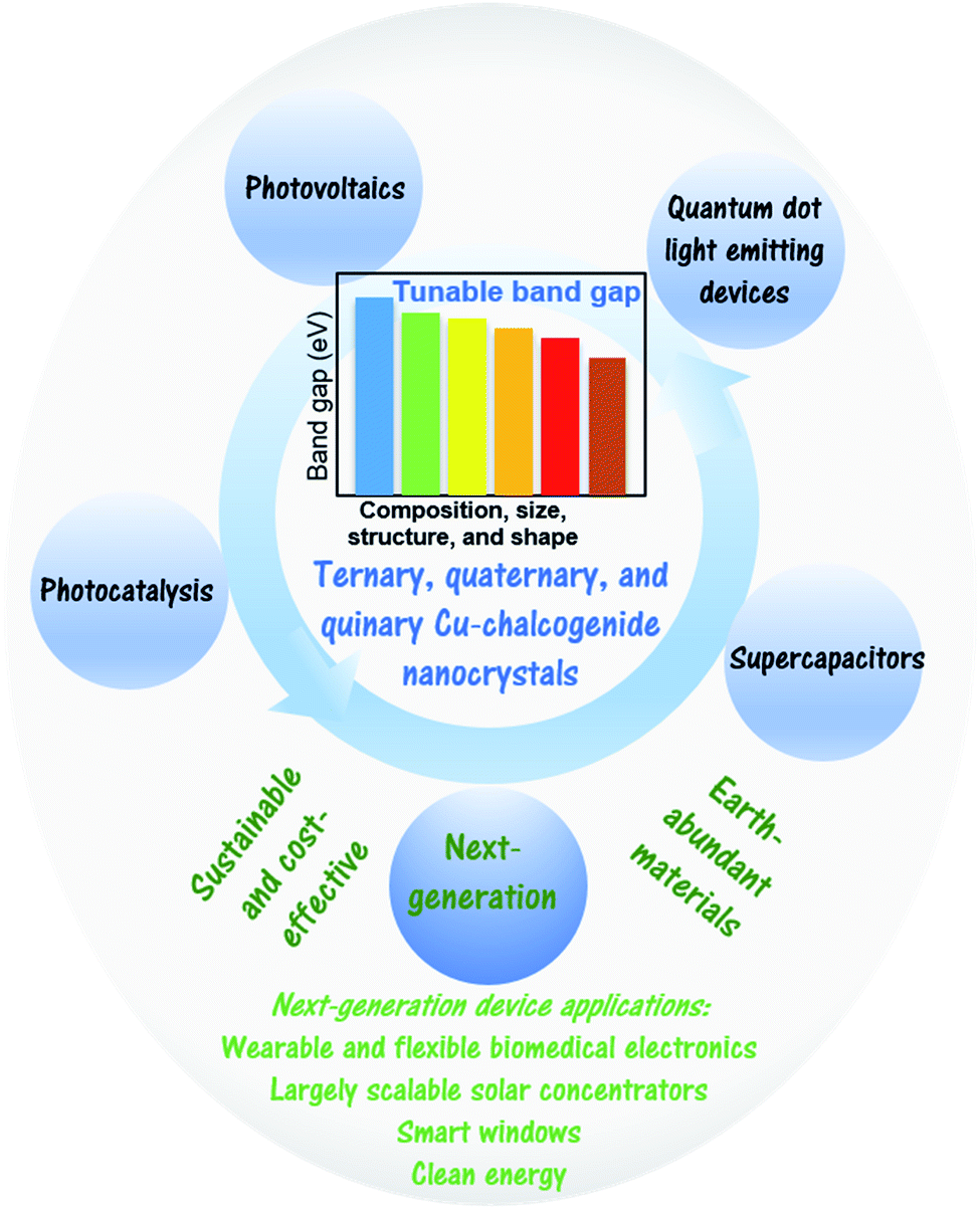 | ||
| Fig. 1 Schematic presenting the advantages and different device applications of multinary Cu-chalcogenide nanocrystals. | ||
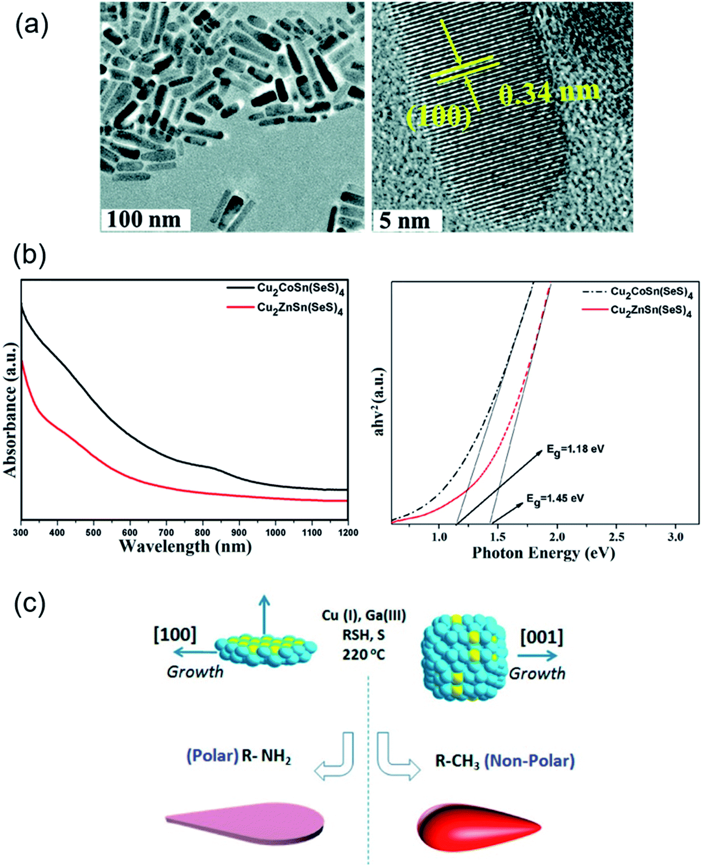 | ||
| Fig. 2 Novel synthesis strategies for multinary Cu-chalcogenide nanocrystal compositions. (a) Transmission electron microscopy (TEM) and high-resolution TEM (HRTEM) images of wurtzite phase Cu2ZnInS4−x (x = 0.5 ± 0.3) nanorods synthesized via a hot-injection technique. Reproduced with permission from ref. 63. Copyright: Chem. Commun., The Royal Society of Chemistry; (b) ultra-violet visible absorption spectra and experimental Tauc plots of Cu2CoSn(SeS)4 and Cu2ZnSn(SeS)4 nanocrystals, Reproduced with permission from ref. 67. Copyright: Sci. Rep., Nature; and (c) schematic showing the formation mechanism of two-dimensional tadpoles and tadpole-like CuGaSe2 nanostructures. Reproduced with permission from ref. 35. Copyright: Chem. Mater., ACS. | ||
(a) Ternary systems
Ternary I–III–VI2 nanocrystals, i.e. CuInE2 (E: S, Se) have been synthesized in the chalcopyrite, wurtzite, and zinc blende phases, but it is difficult to structurally differentiate between the wurtzite and zinc blende products. These semiconductor nanocrystals exhibit direct and narrow band gaps. Balancing the reactivity of Cu and In through complexation of Cu+ with a soft Lewis base like dodecanethiol (DDT) is an important strategy to achieve the chalcopyrite phase of CuInS2.13–15 DDT plays the role of the sulfur source, ligand, and the solvent in these reactions. The optimum reaction temperature lies between 180 and 270 °C for this synthesis to obtain nanocrystal sizes within the quantum confinement regime. Larger CuInS2 chalcopyrite nanocrystals of size 100 nm can be formed with thiourea as a sulfur source and alcohol solvents.16,17 Elemental S and Se are also used as anionic sources for the synthesis of CuInS2 and CuInSe2 chalcopyrite nanocrystals.18,19 This is particularly relevant for CuInSe2 where elemental Se is used with oleylamine as the solvent and ligand to form smaller sized nanocrystals.20,21 The use of ligands like trioctylphosphine, trioctylphosphine oxide or trioctylphosphine with Se powder instead of oleylamine promotes the growth of larger aggregated nanocrystals of CuInSe2.22–24 Alternately, the addition of a weaker binding ligand, dioctylphosphine oxide facilitates formation of anisotropic CuInSe2 structures like nanowires. Other synthesis strategies for CuInSe2 have also been reported with ethylenediamine as a substitute for oleylamine or the use of alkylthiols with Se powder to produce smaller nanocrystals of sizes 3–6 nm.25,26The wurtzite phase of CuInE2 is only stable in the nanocrystal form at room temperature. Alkylamine ligands in combination with DDT as the sulfur source play a major role in stabilizing this crystal phase.27 Oleylamine or ligand mixtures of oleylamine/oleic acid and oleylamine/trioctyphosphine oxide are used with DDT to facilitate wurtzite phase ternary nanocrystals. Metal acetates are common cationic precursors for wurtzite phase CuInS2.28–30 CuInS2 wurtzite nanocrystals have also been synthesized with single source precursors such as (Ph3P)CuIn(SCPh)4 in the presence of trioctylphosphine oxide and DDT using reaction temperatures ranging from 150–250 °C.31 Wurtzite phase CuInSe2 nanocrystals can be obtained with diphenyldiselenide as the anionic precursor in oleylamine and copper oleate and InCl3 as the precursors for the cations.32,33 The formation mechanism of wurtzite phase CuInE2 nanocrystals proceeds through the initial generation of nuclei of the corresponding binary complexes and growth of the ternary wurtzite nanocrystals in the presence of amines.29,30 CuInSe2 nanocrystals have also been reported via a cation exchange approach with anisotropic Cu2−xSe as the template and dodecaneselenol as the phosphine-free Se precursor.34
Das Adhikari et al. have reported the growth of anisotropic, tadpole-like CuGaS2 nanocrystals using elemental S and alkyl thiols as dual sulfur sources with hexadecylamine ligand and metal acetylacetonate precursors and a mixture of octadecene and alkylamine as the solvent.35 Elongated tadpole-like CuGaS2 nanocrystals were also achieved in this synthesis by introducing zinc acetylacetonate in the reaction mixture. CuGaS2 nanostructures were formed from seeds of Cu2S nanodisks in these syntheses.
Our group has reported the first solution-based synthesis strategies for layered ternary CuSbS2 with controlled thickness down to a monolayer.36,37 These materials exhibit a band gap of 1.5 eV in the visible wavelength range and are highly promising for flexible supercapacitor and thin film solar cell applications. A bottom-up approach with elemental sulfur and oleylamine has been used for the formation of CuSbS2 nanoplates with multiple layers. On the other hand, CuSbS2 mesobelts have been synthesized via a hybrid bottom-up-and- top-down approach using 1-DDT and tertiary DDT (tert-DDT) as the sulfur source and an exfoliation strategy to form the controlled layered structure. Copper acetylacetonate and antimony chloride served as the metal precursors for both these syntheses. Ramasamy et al. have also reported a novel synthetic strategy to form all four p-type semiconductor phases of copper antimony sulphide for the first time.38 The synthesis has been achieved with copper acetylacetonate and antimony chloride precursors in oleylamine and elemental S as the anionic precursor.
(b) Quaternary and pseudo-quaternary systems
Quaternary Cu-chalcogenide semiconductor nanocrystals offer a higher level of compositional flexibility to achieve tailored optical band gap and electronic energy levels compared to the ternary and binary complexes. At the same time, these materials are synthetically more challenging to achieve as multiple cations and chalcogen anions are incorporated within the crystal lattice of these systems.Cu(InxGa1−x)Se2 and Cu(InxGa1−x)S2 (CIGS) nanocrystals have also been widely studied for their applications in photovoltaic devices. Alkylamines have been used as the capping agent in combination with Se powder as the anionic precursor for the syntheses of CIGS. The ligands play a major role in determining the final sizes of CIGS nanocrystals. For example, smaller-sized nanocrystals are formed with hexadecyl amine as compared to oleylamine.39 The synthesis with hexadecyl amine proceeds through the formation of metal–ligand complexes, generation of various amorphous binary and ternary nanocrystal compositions and Se nanorods, which finally transform to the CIGS nanocrystals at higher temperatures. The use of single source precursors with ethanedithiol is suitable for the formation of ultra-small CIGS nanocrystals of sizes 2–3 nm.40 DDT and tert-DDT have been used as the S source to achieve tunable tadpole-like and rod-like morphologies of the pure wurtzite phase CIGS nanocrystals.41 Cation exchange has been a key synthetic strategy to overcome the limitation of precursors in direct synthesis for achieving multinary Cu-chalcogenide compositions.42 In cation exchange, the miscibility of the parent compound and the product and the diffusion rate of cations to and from the nanocrystals are controlled through suitable reaction temperatures and concentrations of cations to achieve the desired nanocrystal composition. Recently, conversion of CuInS2 to CuGaInS2 nanocrystals has been achieved via the cation exchange of Cu+ with Ga3+ mediated through GaCl3-L (L: trioctylphosphine, triphenylphosphite, and diphenylphosphine) complexes.42 Cu2ZnSnS4 (CZTS) and Cu2ZnSnSe4 (CZTSe) are the two most widely reported Cu-chalcogenide nanocrystals as they offer a promising and more sustainable platform as absorber layer materials for thin film solar cells.43 The tetragonal kesterite phase is a common structure for these materials in the bulk, in which CuSn and CuZn exist as alternating layers in the direction of the crystal's c-axis. These materials can also exist in the stannite phase where SnZn and Cu form the alternate cation layers of the crystal structure. CZTS can be synthesized via injection of the sulfur source, elemental S, in oleylamine, into a hot solution of metal precursors in oleylamine.44 A second method uses injection of both the elemental S in oleylamine and metal precursors into a hot solution of trioctylphosphine oxide.45 This method facilitated excellent size control and formed CZTS nanocrystals in the size of 12 nm. Small CZTS nanocrystals of sizes between 2 and 7 nm have been synthesized using metal diethyldithiocarbamates with oleylamine.46,47 Another strategy to form CZTS is via heat-up where the metal precursors and S source are mixed in oleylamine at room temperature prior to heating at the reaction temperature, 280 °C.48 The amine ligand and solvent play a key role in the size-controlled synthesis of CZTS nanocrystals. For example, substitution of oleylamine with ethylenediamine forms aggregated particles or wire-like structures.49,50 The use of thiourea as the anionic precursor in an ethylene glycol solvent has also yielded aggregated structures with sizes ranging from 100–500 nm.51,52 The combination of ligand and S source has a strong influence on the phase of the final CZTS nanocrystals. An ethylenediamine ligand in a thiocarbamide sulfur precursor can stabilize the orthorhombic phase of the nanocrystals.53 Alkylthiols as the stabilizing ligand facilitate the formation of wurtzite phase nanocrystals.54,55 Singh et al. introduced the use of both DDT and tert-DDT in the presence of oleylamine to form elongated wurtzite phase nanocrystals of CZTS.56 CZTS has also been synthesized via a novel chemical vapor deposition strategy using diethyldithiocarbamate complexes of copper and zinc and alkyl derivatives of tin as the precursors.57 On the other hand, CZTSSe nanocrystals of smaller sizes (20 nm) are synthesized via hot injection of trioctylphosphine selenide at 295 °C into a solution of metal chloride precursors in octadecene.58 Liu et al. has also established a phosphine-free synthetic strategy for the formation of CZTSSe nanocrystals.59 In this method, CZTSSe nanocrystals of size (3–4 nm) within the quantum confinement regime have been synthesized using hot injection of a solution of Se powder in DDT and oleylamine at 180 °C into a reaction mixture of metal chlorides in oleylamine and DDT. In situ cation exchange has also been applied for effective synthesis of CZTSSe nanoplatelets.60 Recently, greener strategies like aqueous phase synthesis of size-controlled CZTS nanocrystals and CZTSSe have been reported.61,62
Recently, we have reported the synthesis of phase-pure wurtzite Cu2ZnAS4−x and CuZn2AS4 nanorods and nanoworms (A: Al, Ga, In; 0.1 ≤ x ≤ 0.5).63 A one-step hot-injection method using metal-acetylacetonate precursors, a combination of DDT and tert-DDT as anionic precursors, and oleylamine as the ligand and solvent has been applied to form these wurtzite nanocrystals. These nanocrystals can be further transformed to the stannite phase via annealing at high temperatures (400–500 °C). These materials show a composition-controlled direct band gap in the visible regime, which is attractive for photovoltaic applications. Our group has also reported the synthesis of oblate spheroid and triangular plate-shaped Cu2FeSnS4 (CFTS) nanocrystals with band gaps 1.54 and 1.46 eV, respectively using a similar solution-chemistry approach.64 New quaternary CuMSnS4 (M = In, Ga) nanocrystals have been synthesized in the wurtzite phase via a hot-injection method using a combination of n-DDT and t-DDT.65 These nanocrystals exhibit strong visible light absorption, highly attractive for energy conversion applications.
Bera et al. have developed a thermodynamically controlled approach for the synthesis of a family of monodisperse Cu12−xMxSb4S13 (M = ZnII, CdII, MnII, and CuII) tetrahedrite semiconductor nanostructures.66 This has been achieved through prevention of cross-nucleation reactions with minimized reaction time in these syntheses.
(c) Quinary systems
Few reports are available on quinary Cu-chalcogenide systems due to the increased complexity in synthesis as compared to the quaternary and pseudo-quaternary compositions. In situ partial cation exchange has been used as a synthetic strategy for formation of plate-like copper zinc tin selenide-sulfide semiconductor nanocrystals.60 Ozel et al. synthesized Cu2CoSn(SeS)4 and Cu2ZnSn(SeS)4 nanocrystals as catalysts for use as counter electrodes in dye-sensitized solar cells using a hot-injection approach.67 A solution of metal precursors in the oleylamine ligand is heated to 280 °C, before injection of a solution of elemental S in oleylamine into the reaction mixture and heating at 280 °C for 30 min. These nanocrystals are 18–25 nm in size with a kesterite structure and optical band gaps of 1.18 eV and 1.45 eV. Recently, wurtzite phase CuNixZn2−xInS4 (x = 0–2) semiconductor nanocrystals have been reported with a tunable band gap in the visible range between 1.44 and 2.20 eV.68 In this synthetic strategy, metal acetylacetonate precursors are heated to dissolution at 110 °C in oleic acid as the capping agent. DDT serves as the sulfur precursor and is quickly injected into the reaction mixture at 150 °C, followed by heating of the reactants at 210 °C. The formation mechanism of these nanocrystals proceeds through the initial generation of spherical CuZn2InS4 nanocrystals, which transform to the final bullet-shaped CuNixZn2−xInS4 nanocrystal product.Emerging characterization techniques
Material characterization is an important component for bridging the path from synthesis of the new multicomponent Cu-chalcogenides to application. Transmission and scanning electron microscopy have been widely applied to investigate the size, morphology, and elemental composition of these nanocrystals. X-ray diffraction and X-ray photoelectron spectroscopy served as the golden standard to explore the crystal phase and oxidation state of the new nanocrystals. Grazing incidence small angle scattering and neutron scattering are also used to differentiate between two similar crystal phases. The experimental band gap of these nanostructures is typically measured using ultraviolet visible absorption spectroscopy and generation of Tauc plots. Recently, a few other characterization techniques have emerged that can be promising in predicting the unique properties of multicomponent chalcogenide nanocrystals.(a) Hyperspectral infrared nanoimaging
Recently, hyperspectral infrared nanoimaging using nano-Fourier transform infrared spectroscopy (nano-FTIR) has been used in quantitative analysis of semiconductor samples and polymers (Fig. 4).69,70 This technique is rapid and non-invasive and can serve as a platform for mapping the chemical distribution of cations and anions with a spatial resolution in multinary Cu-chalcogenide nanocrystals. The method is based on atomic force microscopy (AFM) principles, where the AFM tip concentrates the incident monochromatic or broadband infrared radiation field to a nanoscale spotsize at its apex. The scattered infrared field from the AFM tip is detected via an interferometer to generate two-dimensional infrared amplitude and phase images of the sample. The possibility of mapping chemical distribution and interactions within the nanocrystals is much sought after from the perspective of multinary chalcogenide structures, and one that may be achieved through hyperspectral infrared nanoimaging.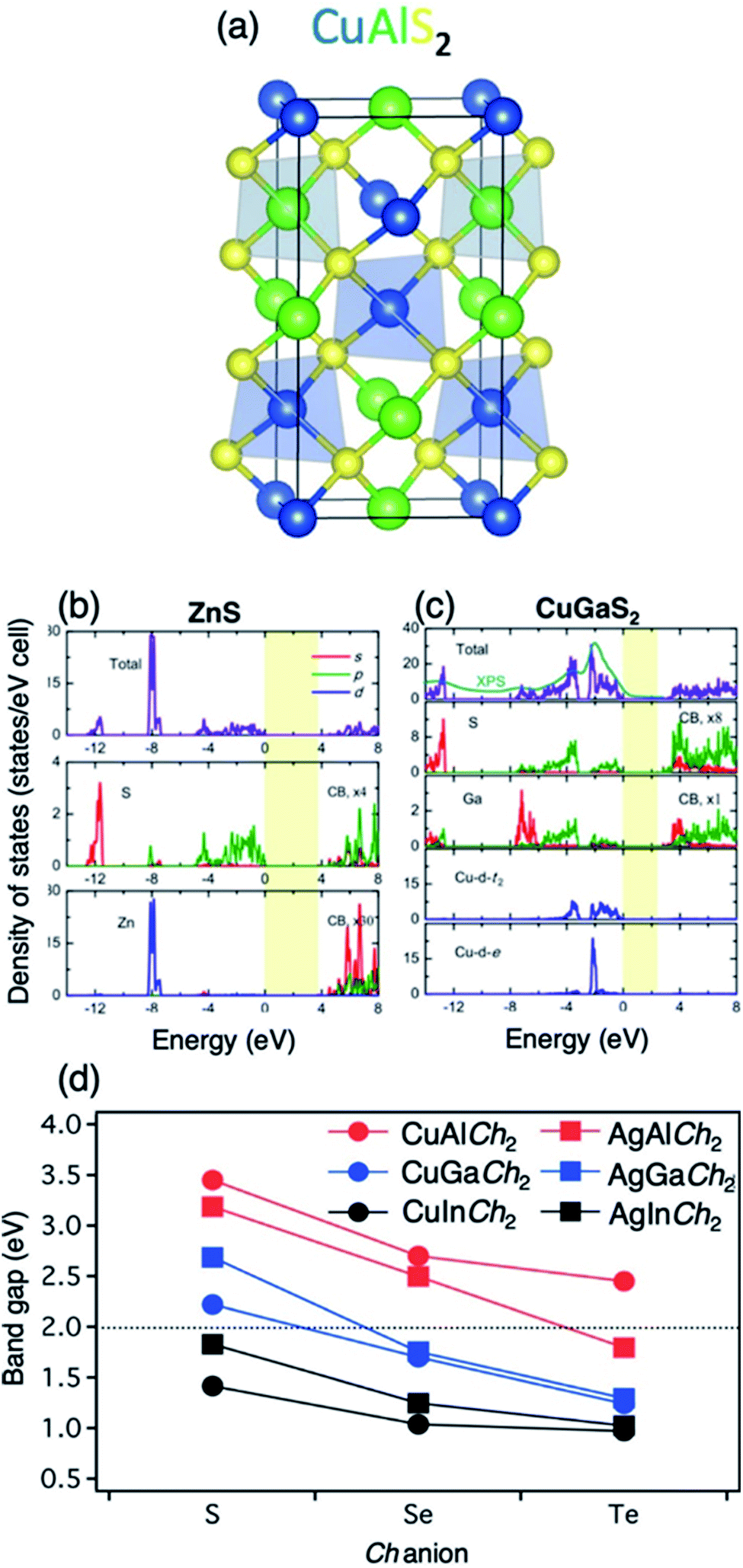 | ||
| Fig. 3 Illustration of (a) the chalcopyrite structure, represented by CuAlS2, and the DFT+U+G0W0 density of states from Zhang et al.76 of (b) zinc blende ZnS compared to (c) chalcopyrite CuGaS2, indicating p–d hybridization at the VBM in the chalcopyrite structure. Reproduced with permission from ref. 76 Copyright: Comput. Mater. Sci., Elsevier, and (d) experimentally measured band gaps of I–III-Ch2 semiconductors. Reproduced with permission from ref. 73. Copyright: Chem. Rev., ACS. | ||
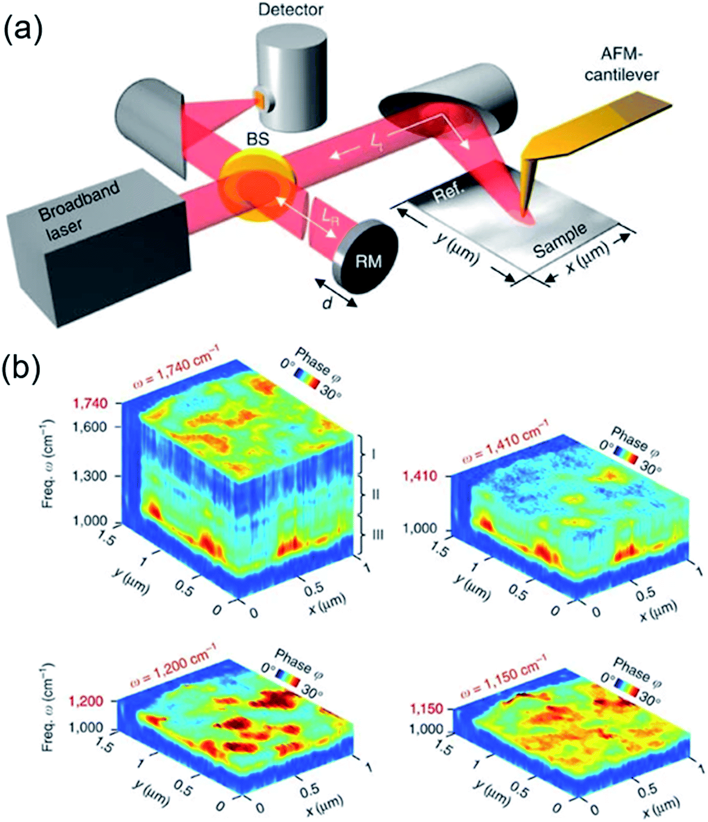 | ||
| Fig. 4 Hyperspectral infrared nanoimaging. (a) Set-up of the instrument employing a mid-infrared laser continuum source for tip illumination and (b) hyperspectral infrared data cubes of a spectral resolution of 35 cm−1, cut at different frequencies ω. They show the normalized phase ϕ of the tip-scattered light as a function of position (x, y) and frequency ω. Reproduced with permission from ref. 69. Copyright: Nat. Commun., Nature. | ||
(b) Thermogravimetric analysis
Thermogravimetric analysis (TGA) offers key information about the weight fraction and composition of the surface stabilizers on nanocrystals. Riedinger et al. used in situ TGA analysis during a solvent-free synthesis of CdSe nanocrystals to identify reactive organo-chalcogenide intermediate complexes.71 These complexes have facilitated the molecular design of new precursor materials for CdSe nanocrystals. A similar TGA-based approach may be suitable in identification and molecular design of new precursor complexes for the multinary Cu-chalcogenide nanocrystals.(c) Computational band gap predictions
Computational methods can be used to predict the band gap and absorption band edge of chalcogenide semiconductors. Several studies have applied density functional theory (DFT) calculations to determine the band gap (Eg) of new materials.63,72 DFT is a fast and effective strategy for calculating the minimum energy gap between the valence band maxima and conduction band minima, but the method compromises the accuracy of band gap calculations for better computational efficiency. In some cases, these calculations may lead to underestimation of band gaps unless the parameters are empirically adjusted. Therefore, more computationally expensive methods like HSE06, many body perturbation theory (GW), and GW with the Beth–Salpeter equation (GW-BSE) are being investigated for band gap estimation of chalcogenide semiconductors on a case-by-case basis (Fig. 3).73–76Applications
(a) Photovoltaics
The global energy demand is expected to reach 28 TW by 2050 with the increasing global population. This poses a burden on the finite fossil fuel energy sources. There is a growing demand for sustainable and cleaner energy and in 2017 solar photovoltaics (PV) have constituted 1.8% of the world's electricity with nearly 98 GW of new installations.77,78 Silicon is the dominant material for PV devices with the highest recorded energy conversion efficiency of 26.7% using the heterojunction technology.79 However, Si has an indirect band gap and the contacts in Si-based devices are made of Ag, which is found in limited quantities in the earth.80 CdTe, CIGS, and CIGSe are the other most dominant absorber layer materials for thin-film solar cells, with CIGSe showing nearly 22.6% efficiency.4,80–86 However, the limited availability and toxicity of these materials as well as the increased thickness of the device are some areas of improvement.87 To this end, there have been several investigations in the past decade on quaternary CZTS solar cells. They are composed of cost-effective and easily available elements, but the highest efficiency of the kesterite phase CZTS and CZTSSe devices reached 9.2% and 12.6%, respectively.5,88–92 There is further room for improvement because the thin film PV devices using viable materials and new earth-abundant multinary Cu-chalcogenides (e.g., Cu2FeSnS4 (CFTS), Cu2MnSnS4 (CMTS), Cu2BaSnS4 and Cu2BaSn(S,Se)4 (CBTS and CBTSSe), Cu2NiSnS4 (CNTS), and Cu2CoSnS4) are currently being investigated for PV applications.83,93 All these multinary Cu-chalcogenides show a suitable absorption coefficient (>104 cm−1) and a band gap within the visible light range.81 A key research thrust for these viable PV materials is to achieve better conversion efficiencies.The p-type CFTS, being cheap and having a suitable band gap,64 has been prepared as an absorber layer for thin film solar cells using cost-effective non-vacuum approaches. The best efficiency (e.g., 2.95%) for CFTS has been reported with CFTS/Bi2S3 heterojunctions prepared via the SILAR method.94 The SILAR technique for CFTS thin films was first reported by Guan et al.95 Meng et al. fabricated CFTS solar cells with 0.11% efficiency via a sputtering approach.96 CFTS thin films have been reported through several synthesis techniques such as electrostatic field assisted spray pyrolysis, aerosol assisted chemical vapor deposition, doctor blade deposition, and electrochemical deposition.97–100 CMTS is another cost-effective p-type semiconductor that has been investigated in recent years as an absorber layer for thin film solar cells. CMTS thin films have been deposited on glass substrates via chemical routes.101,102 These are most commonly found in the stannite phase. Direct liquid coating and annealing under a N2 atmosphere has also been employed for preparation of CMTS thin films. These films showed an efficiency of 0.49%.103 One of the highest efficiencies for CMTS PV devices (i.e., 0.73%) has been achieved using Na doping between the CMTS layers via a spray technique to enhance grain growth.104 In addition, the annealing conditions have a major influence in further enhancing the efficiency (e.g., 0.83%) of CMTS solar cells.105,106 There are currently a few literature reports on CNTS thin film solar cells and most of the studies have employed non-vacuum techniques like electrodeposition, spraying, and direct liquid coating.107–110 Some of the limiting factors in increasing the efficiency of CZTS solar cells are the Cu-on-Zn and Zn-on-Cu antisite disorders.111 CBTS does not exhibit these cation–cation antisite disorders and is a promising candidate for achieving higher efficiencies in thin film solar cells.112 The CBTS and CBTSSe thin films have been prepared via vacuum deposition techniques in the few recent reports available on this material.113 An efficiency of 5.2% has been obtained with a CBTSSe-based PV device.114 Se substitution, band gap engineering, and post annealing in air have been used as strategies to enhance the performance of CBTS/CBTSSe thin film solar cells. Our group and others have investigated CCdTS/CCdTSSe nanocrystals and thin films for PV devices as Cd minimizes the detrimental ZnCu antisite defects.115–117 A maximum efficiency of 3.1% has been achieved with these materials.118 New multicomponent Cu-chalcogenides continue to be explored for higher efficiencies, cost-effectiveness, and viable alternatives for PV applications.
(b) Photocatalysis
Photocatalysis is an important scheme for clean energy production and environmental remediation.119,120 The two major applications of photocatalysis are in hydrogen fuel generation through water-splitting reaction using sunlight and in the degradation of pollutant dyes for wastewater remediation.121–123 TiO2 nanoparticles have been traditionally used as photocatalysts for these reactions, but the wide band gap of the metal oxide based materials allows absorption of a small fraction of the solar spectrum within the ultraviolet region. Multinary chalcogenide nanocrystals are some of the most promising semiconductor photocatalysts with a suitable band gap for absorption in the visible light range.To this end, ternary CuInS2/ZnS nanorods have shown significant efficiency in H2 generation from an aqueous solution containing S2− and SO32− as sacrificial reducing agents.124 The H2 production rate has been further increased in this reaction through addition of stable cocatalysts like Pt and Pd4S nanocrystals on the surface of CuInS2/ZnS nanorods. Another report established the high photocatalytic activity of alloyed Zn1.6Cu0.2In0.2S2 (ZCIS) microspheres for H2 generation with a 15.45% quantum yield at 420 nm under Ru-loading.125 This study also proved that smaller crystallite size of the semiconductor photocatalysts plays a key role in enhancing H2 production. Qian et al. have shown the effect of semiconductor nanocrystal composition on photocatalytic H2 generation rates using different compositions of ZCIS nanocrystals of 10 nm in size.126 The Zn1.6Cu0.2In0.2S2 nanocrystal, showing a H2 production rate of 984 μmol g−1 h−1 without any cocatalysts is the most favorable composition in this case too. This exceptional photocatalytic behavior of Zn1.6Cu0.2In0.2S2 semiconductor nanocrystals is attributed to the combined effect of a suitable band structure and excellent charge separation ability of these nanocrystals. Similar investigations of the effect of alloy compositions on photocatalytic H2 yield have been conducted with the quaternary Cu(InxGa1−x)S2 chalcogenide nanorods.127 It has been observed that there is an optimum level for substitution of In with Ga in these nanocrystal systems to achieve the maximum H2 yield. The highest H2 evolution has been obtained with the CuIn0.3Ga0.7S2 compositions. Substitution of In with Ga raises the conduction band of the CIGS semiconductor nanocrystals and facilitates increased density of photogenerated electrons for enhanced reduction of H2O to H2. However, increasing the Ga concentration beyond the optimal limit induces wider band gaps that are unfavorable for photon absorption and photogenerated charge carrier density. The quaternary composition, CZTS has shown promising results for H2 evolution in the presence of cocatalysts (e.g., Au and Pt) that can induce enhanced separation of the charge carriers.128–130 The crystal phase of the CZTS nanocrystals plays a strong role in the photocatalytic activity.130 For example, the kesterite phase of CZTS is known to show a higher H2 evolution rate than the wurtzite phase. The kesterite phase, formed through thermal annealing of the wurtzite nanocrystals, has a higher crystallinity and fewer defects than the wurtzite phase. This can likely account for enhanced photocatalytic behavior of the kesterite phase as defects act as recombination sites for the charge carriers and reduce the overall photocatalytic activity.
Visible light-driven photocatalysis is an effective and environment-friendly approach to render the non-biodegradable industrial dyes (e.g., rhodamine B (RhB) and methylene blue) less toxic via degradation prior to release. RhB, a commonly used dye has been shown to degrade significantly by 91% within 2 h in the presence of ZCIS nanorods.124 The degradation can be easily measured through time-dependent absorption spectra of the dye showing its marked decrease in concentration. In case of the ZnS-coated ZCIS nanorods, the RhB chromophore degraded completely via the formation of N-deethylated intermediates.131 Other ternary and quaternary Cu-chalcogenide nanocrystals (e.g., CZTS, CuGaS2, and Cu2ZnGeS4) have also been effective in the degradation of dyes, but at a slower rate compared to the ZCIS nanorods.132–134 CZTS nanocrystals coupled with Au or Pt metals show a higher photocatalytic activity for dye degradation compared to the unmodified CZTS nanocrystals.128 The ternary CuInSe2 and CuInS2 chalcogenide nanocrystals have been known to serve as sensitizing agents for TiO2 and ZnO platforms for photocatalytic degradation of dyes.135,136
(c) Quantum dot light emitting diodes
The advantage of quantum dot light emitting devices (QLEDs) over devices based on organic, polymeric, and inorganic materials is a combination of transformative color purity and brightness, lower turn-on voltage (<2 V), and an ultrathin active layer that facilitates device flexibility in the QLEDs.25,137,138 A typical QLED consists of an anode, an electron transport material (ETM), a nanocrystal active layer, a hole transport material (HTM), and a cathode. Charge carriers from the respective charge transport layers (CTL) undergo radiative recombination in the nanocrystal active layer to generate the characteristic electroluminescence of the device. Currently, the visible light devices rely on Cd-chalcogenides and the Pb-chalcogenides predominate the near-infrared applications. In comparison, the Cu-based chalcogenides are composed of earth-abundant materials and provide a more sustainable platform for QLED applications. The multinary transition metal Cu-chalcogenide nanocrystals can be most attractive active layer materials for QLEDs due to their composition, size, and defect-dependent spectral emission.2,6,139,140 The high energy states of the Cu 3d orbitals allow hybridization with the de-localized chalcogen-p orbitals.6 This strong p-d hybridization and the comparable size and electronegativity between the transition metal cations and the chalcogens facilitate a large adjustable range of optoelectronic properties in these compounds. The defect concentrations and the possibility of non-stoichiometric and antisite defects in the Cu-chalcogenides can be used to further tailor the spectral and electroluminescence properties of these compounds.141–143 The multinary Cu-chalcogenides exhibit size-dependent donor–acceptor pair recombination related photoluminescence properties. Several ZnS-shelled ternary and quaternary Cu-chalcogenide nanocrystal platforms like Mn doped CuInZnS,144 CuInS2/ZnS,145–148 CuInSe2/ZnS,25 CuInZnS/ZnS,149 CuInGaS/ZnS,150 and mixed systems of CuInS2/ZnS and ZnCdSe/ZnS143 have been promising for this type of QLED devices.141 The current goals from a device performance perspective are to achieve miniaturization and structural flexibility, prevent loss of charge carriers and non-radiative recombination, and facilitate effective recombination of charge carriers within the emissive layer. To this end, a dominant trend in these Cu-chalcogenide nanocrystal systems is to increase quantum efficiency and resistance to photobleaching through synthetic control. For example, the molar ratio of Cu![[thin space (1/6-em)]](https://www.rsc.org/images/entities/char_2009.gif) :In is adjusted in the CuInS-based systems to achieve better electroluminescence properties.
:In is adjusted in the CuInS-based systems to achieve better electroluminescence properties.
Another emerging and less explored application of semiconductor nanocrystals is in quantum dot white light emitting diodes (WLEDs). The WLEDs are currently aimed at achieving emissions comparable to a blackbody and are therefore highly useful as a large area lighting source, sunlight simulator, and as backlight sources for displays. WLEDs are more environment-friendly and consume less energy compared to the conventional light sources. The nanocrystal-based WLED devices started with a blue or UV light source being coupled with a small band gap down-conversion active material layer.151–153 However, they have suffered from low external quantum efficiency (EQE) due to reabsorption of high-energy photons by the NCs, photobleaching, and non-uniform distribution of charge carriers. Broader emission spectra of the conventional light sources is also a disadvantage for these WLEDs. Therefore, the next class of devices, pioneered by Bawendi and Bulovic has been designed with a mixture of different light emitting nanocrystals to form electroluminescence-based WLEDs with higher color rendering index (CRI) and color purity.154–156 The emission spectrum in these WLEDs can be precisely optimized with the appropriate ratio of red, green, and blue (RGB) emitting nanocrystals.154,157,158 However, the wide gap in bandwidth between the various emitters is a limitation and adversely affects the color purity of the device. It has been later discovered that increasing the number of different types of emitter NCs (e.g., blue, cyan, yellow, and red) can significantly improve the CRI. Recent technological advances in WLED have also shown a huge impact of ETM and HTM on the device performance (Fig. 5).147,159,160 So far, ZnO nanocrystals have shown excellent charge mobility as the ETM and hybrid polymeric layers have been widely used as the HTM in WLED fabrication. The Cd-based materials (e.g., CdSe–CdS core–shell nanocrystals) dominate the WLED applications, but more viable alternatives are currently being sought.6,161,162 Materials that can increase the device lifetime are being investigated to further enhance and transform the WLED technology. Cu-based chalcogenides are a suitable candidate for WLEDs due to their inherent broad emission range.163 The emission spectra can be further broadened through addition of dopants like Mn, Sn, and Ga in the Cu-chalcogenide nanocrystal structures.144,145,164,165 To this end, multiple Cu-chalcogenide compositions have been successfully applied in WLEDs. For example, multinary Cu–Sn–In–S, CuInS2, and Mn-doped Cu–In–Zn–S nanocrystals have been promising for electroluminescence type WLEDs.143–145,166 Cu-chalcogenides have also been applied in WLEDs using down-conversion technology where the blue or UV-light is partially or fully converted to visible light.165,167–173 The CIS/ZnS semiconductor nanocrystals and ZCIS alloy nanocrystals are most commonly used in down-conversion WLEDs.174 Recently, Liu et al. have reported a new WLED composed of highly luminescent Cu–In–Zn–S nanocrystals showing a nearly 90% photoluminescence quantum yield.175
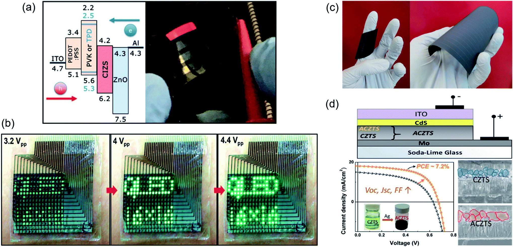 | ||
| Fig. 5 Energy conversion and energy harvesting applications of multi-component Cu-chalcogenide nanocrystals. (a) Red-emitting QLEDs fabricated using CuInS2–ZnS nanocrystals and two different HTMs (polyvinylcarbazole and poly(4-butylphenyldiphenylamine)). Reproduced with permission from ref. 147. Copyright: ACS Appl. Mater. and Interfaces, ACS; (b) ultra-thin QLED display in a wearable device showing sequential images at different operating voltages. Figure reproduced with permission from ref. 138. Copyright: Adv. Mater., Wiley; (c) photo of highly flexible CIGS modules on two different substrates, (left) polyimide substrate showing strong curling behavior and (right) a steel substrate with lower curling behavior. Reproduced with permission from ref. 86. Copyright: Engineering, Elsevier; and (d) incorporation of Ag reduces the antisite defects and improves the grain size of kesterite-phase CZTS, facilitating an enhancement in open-circuit voltage and efficiency of the thin film solar cell. Reproduced with permission from ref. 5. Copyright: ACS Energy Lett., ACS. | ||
(d) Supercapacitors
Supercapacitors are an important class of sustainable energy storage devices due to their inherently high power density, longevity, and rapid charge/discharge capacity. Ternary and quaternary Cu-chalcogenide nanocrystals have served as attractive electrode materials for pseudocapacitive and electric double layer supercapacitors in recent studies.176,177 For example, hydrothermally synthesized CFTS nanocrystals have exhibited excellent electrical double layer capacitor characteristics and unique photo-enhanced supercapacitive behavior.178 The charge–discharge time and hence capacitance of these materials increase upon light irradiation. Our group has reported the promising specific supercapacitance and high cycling stability of layered copper antimony chalcogenide mesocrystals.37,179 These electrodes have shown no loss of capacitance in cyclic voltammetry (CV) measurements even after 1000 cycles using different alkali metal ion electrolytes (e.g., LiOH, NaOH, and KOH). In fact, the materials exhibit an improvement in charge-storage capacity after 200 cycles. Recently, ternary Cu3SbS4 and Cu3MoS4 grown on Ni foam have served as excellent binder-free electrodes for asymmetric supercapacitors.180 These materials achieved the desirable combination of a high specific device capacitance of 213.6 F g−1, excellent energy (58.15 W h kg−1) density, better life-cycle, and maximum power density (6363.63 W kg−1) for supercapacitor device applications.(e) Luminescent solar concentrators
Luminescent solar concentrators are unique antenna-like structures to harvest and concentrate solar energy through a combination of photon absorption, luminescence, and waveguiding. The resulting high irradiance and narrowband output light is highly beneficial for solar energy conversion devices. In a simplest luminescent solar concentrator, a substrate of polymer or glass acts as a waveguide platform with the luminophores either embedded or coated on top. These devices are characterized through a combination of geometrical concentration factors and optical efficiency as performance indicators. Luminophore reabsorption losses remain the major limiting factors and possible areas of improvement for future large-scale luminescent solar concentrator technologies. To this end, semiconductor chalcogenide nanocrystals can be excellent candidates as spectral conversion phosphors for large scale luminescent solar concentrators.181 Tunable properties and solution based processing approaches of the nanocrystals enable new engineered materials and cheaper fabrication methods for the luminescent solar concentrators. Doped nanocrystals such as Cd1−xCuxSe have been promising in minimizing reabsorption losses.182 Meinardi et al., used CuInSexS2−x nanocrystals embedded in photo-polymerized poly(lauryl methacrylate) to realize materials that exhibit no distortion to perceived colors.183 These materials are attractive for the photovoltaic window technology. These nanocrystals minimize the reabsorption mechanisms and can therefore, realize a high optical power efficiency of 3.2%. It has been shown that clustering of nanocrystals in the polymer matrix is a possible cause of limiting optical efficiency in large geometries due to light scattering losses.184 Optimizing the nanocrystal concentrations can be the key to overcome light scattering losses. Sumner et al. realized optical power efficiencies up to 5.7% using an optimized concentration of CuInS2/CdS nanocrystal phosphors. Recently, Liu et al. have reported heavy metal free luminophores for liquid solar concentrators using Cu-doped ZnInSe nanocrystals.185 The materials have exhibited an optical efficiency of more than 3.5%, which is two times higher than polymer-based liquid solar concentrators. The highest recorded optical efficiency to date has been reported using high quantum yield (>90%), near-infrared emitting CuInS2/ZnS nanocrystals in a polymer interlayer between glass substrates.186 These laminated glass luminescent solar concentrators have shown an optical efficiency of 8.1% with nearly 44% transmission of visible light, which is highly attractive for windows. While luminescent solar concentrators have traditionally been used to harvest sunlight for photovoltaic devices recent progress has shown the application of CuInSexS2−x/ZnS chalcogenide nanocrystals in novel optical fibre technology, broadband light sources for medical diagnostics, spectral conversion and light-guided agricultural devices, and large-area broadband detectors for telecommunications.187Future perspective
In this review, we have summarized the recent advances made in the synthetic strategies, characterization techniques, and device applications for multinary Cu-chalcogenide semiconductor nanocrystals. The Cu-chalcogenide nanocrystals are less toxic compared to their Cd and Pb-based counterparts and are composed of more sustainable and earth-abundant elements. Recent progress in the synthesis of multinary chalcogenide compositions offer a wider spectrum of structural and compositional flexibility to achieve more tailored properties with the nanocrystals. This opens a wide scope of possibilities for next-generation devices. The multinary Cu-chalcogenides can catalyze new innovations in the field of wearable and flexible biomedical electronics.188 For example, flexible QLEDs using multinary nanocrystals can be interfaced with sensors, resistive random access memory devices, and Bluetooth units to realize touch-sensitive displays, wearable biosensors for measuring heart-rate or motion detection, portable touch sensors for self-monitoring vital signs, and smart glasses to enhance perception of real-time images. The multinary Cu-chalcogenides can also be used as largely scalable luminescent solar concentrator materials for energy-harvesting smart windows.184 At the same time, these novel compositions can pave the way to high-throughput photovoltaic devices and higher efficiency photocatalytic reactions towards a more sustainable and cleaner conversion and harvesting of energy.Conflicts of interest
There are no conflicts to declare.Acknowledgements
SP thanks the National Science Foundation (NSF) for the funding and support provided through the NSF REU Award #1852042. AG thanks the NSF for the funding and support provided through Grant No. CHE-1508259.References
- O. Yarema, M. Yarema and V. Wood, Chem. Mater., 2018, 30, 1446 CrossRef CAS.
- C. Coughlan, M. Ibanez, O. Dobrozhan, A. Singh, A. Cabot and K. M. Ryan, Chem. Rev., 2017, 117, 5865 CrossRef CAS PubMed.
- O. Stroyuk, A. Raevskaya and N. Gaponik, Chem. Soc. Rev., 2018, 47, 5354 RSC.
- T. Feurer, P. Reinhard, E. Avancini, B. Bissig, J. Lockinger, P. Fuchs, R. Carron, T. P. Weiss, J. Perrenoud, S. Stutterheim, S. Buecheler and A. Tiwari, Prog. Photovoltaics, 2017, 25, 645 Search PubMed.
- A. Guchhait, Z. Su, Y. Tay, S. Shukla, W. Li, S. Leow, J. Tan, S. Lie, O. Gunawan and L. Wong, ACS Energy Lett., 2016, 1, 1256 CrossRef CAS.
- K. Knowles, K. Hartstein, T. Kilburn, A. Marchioro, H. Nelson, P. Whitham and D. Gamelin, Chem. Rev., 2016, 116, 10820 CrossRef CAS PubMed.
- S. Chen, X. Gong, A. Walsh and S. Wei, Phys. Rev. B: Condens. Matter Mater. Phys., 2009, 79, 165211 CrossRef.
- Y. Chen, X. Feng, M. Liu, J. Su and S. Shen, Nanophotonics, 2016, 5, 524 Search PubMed.
- J. Chang and E. R. Waclawik, RSC Adv., 2014, 4, 23505 RSC.
- P. Matthews, P. McNaughter, D. Lewis and P. O'Brien, Chem. Sci., 2017, 8, 4177 RSC.
- D. Aldakov, A. Lefrancois and P. Reiss, J. Mater. Chem. C, 2013, 1, 3756 RSC.
- D. Moodelly, P. Kowalik, P. Bujak, A. Pron and P. Reiss, J. Mater. Chem. C, 2019, 7, 11665 RSC.
- X. Tang, W. Cheng, E. Choo and J. Xue, Chem. Commun., 2011, 47, 5217 RSC.
- M. Gromova, A. Lefrancois, L. Vaure, F. Agnese, D. Aldakov, A. Maurice, D. Djurado, C. Lebrun, A. de Geyer, T. Schulli, S. Pouget and P. Reiss, J. Am. Chem. Soc., 2017, 139, 15748 CrossRef CAS PubMed.
- L. Li, A. Pandey, D. Werder, B. Khanal, J. Pietryga and V. Klimov, J. Am. Chem. Soc., 2011, 133, 1176 CrossRef CAS PubMed.
- C. Yu, J. Yu, H. Wen and C. Zhang, Mater. Lett., 2009, 63, 1984 CrossRef CAS.
- K. Das, S. Panda, S. Gorai, P. Mishra and S. Chaudhuri, Mater. Res. Bull., 2008, 43, 2742 CrossRef CAS.
- A. Pein, M. Baghbanzadeh, T. Rath, W. Haas, E. Maier, H. Amenitsch, F. Hofer, C. Kappe and G. Trimmel, Inorg. Chem., 2011, 50, 193 CrossRef CAS PubMed.
- M. Chiang, S. Chang, C. Chen, F. Yuan and H. Tuan, J. Phys. Chem. C, 2011, 115, 1592 CrossRef CAS.
- B. Koo, R. Patel and B. Korgel, J. Am. Chem. Soc., 2009, 131, 3134 CrossRef CAS PubMed.
- A. de Kergommeaux, A. Fiore, N. Bruyant, F. Chandezon, P. Reiss, A. Pron, R. de Bettignies and J. Faure-Vincent, Sol. Energy Mater. Sol. Cells, 2011, 95, S39 CrossRef CAS.
- J. He, W. Zhou, M. Li, Z. Hou, Y. Du and S. Wu, Mater. Lett., 2012, 66, 96 CrossRef CAS.
- S. Wark, C. Hsia, Z. Luo and D. Son, J. Mater. Chem., 2011, 21, 11618 RSC.
- A. Wooten, D. Werder, D. Williams, J. Casson and J. Hollingsworth, J. Am. Chem. Soc., 2009, 131, 16177 CrossRef CAS PubMed.
- H. Zhong, Z. Wang, E. Bovero, Z. Lu, F. van Veggel and G. Scholes, J. Phys. Chem. C, 2011, 115, 12396 CrossRef CAS.
- H. Zhong, Y. Li, M. Ye, Z. Zhu, Y. Zhou, C. Yang and Y. Li, Nanotechnology, 2007, 18, 025602 CrossRef.
- D. Pan, L. An, Z. Sun, W. Hou, Y. Yang, Z. Yang and Y. Lu, J. Am. Chem. Soc., 2008, 130, 5620 CrossRef CAS PubMed.
- M. Kruszynska, H. Borchert, J. Parisi and J. Kolny-Olesiak, J. Am. Chem. Soc., 2010, 132, 15976 CrossRef CAS PubMed.
- S. Connor, C. Hsu, B. Weil, S. Aloni and Y. Cui, J. Am. Chem. Soc., 2009, 131, 4962 CrossRef CAS PubMed.
- X. Lu, Z. Zhuang, Q. Peng and Y. Li, Crystengcomm, 2011, 13, 4039 RSC.
- S. Batabyal, L. Tian, N. Venkatram, W. Ji and J. Vittal, J. Phys. Chem. C, 2009, 113, 15037 CrossRef CAS.
- B. Tappan, G. Barim, J. Kwok and R. Brutchey, Chem. Mater., 2018, 30, 5704 CrossRef CAS.
- D. Houck and B. Korgel, Chem. Mater., 2018, 30, 8359 CrossRef CAS.
- A. Berends, W. van der Stam, Q. Akkerman, J. Meeldijk, J. van der Lit and C. Donega, Chem. Mater., 2018, 30, 3836 CrossRef CAS PubMed.
- S. Das Adhikari, A. Dutta, G. Prusty, P. Sahu and N. Pradhan, Chem. Mater., 2017, 29, 5384 CrossRef.
- K. Ramasamy, H. Sims, W. Butler and A. Gupta, J. Am. Chem. Soc., 2014, 136, 1587 CrossRef CAS PubMed.
- K. Ramasamy, R. K. Gupta, S. Palchoudhury, S. Ivanov and A. Gupta, Chem. Mater., 2014, 27, 379 CrossRef.
- K. Ramasamy, H. Sims, W. Butler and A. Gupta, Chem. Mater., 2014, 26, 2891 CrossRef CAS.
- M. Ahmadi, S. Pramana, L. Xi, C. Boothroyd, Y. Lam and S. Mhaisalkar, J. Phys. Chem. C, 2012, 116, 8202 CrossRef CAS.
- C. Sun, J. Gardner, G. Long, C. Bhattacharya, A. Thurber, A. Punnoose, R. Rodriguez and J. Pak, Chem. Mater., 2010, 22, 2699 CrossRef CAS.
- A. Wang, X. Zhang, N. Bao, B. Lin and A. Gupta, J. Am. Chem. Soc., 2011, 133, 11072 CrossRef PubMed.
- S. Hinterding, A. Berends, M. Kurttepeli, M. Moret, J. Meeldijk, S. Bals, W. van der Stam and C. Donega, ACS Nano, 2019, 13, 12880 CrossRef CAS PubMed.
- K. Ramasamy, M. A. Malik and P. O'Brien, Chem. Commun., 2012, 48, 5703 RSC.
- Q. Guo, H. Hillhouse and R. Agrawal, J. Am. Chem. Soc., 2009, 131, 11672 CrossRef CAS PubMed.
- S. Riha, B. Parkinson and A. Prieto, J. Am. Chem. Soc., 2009, 131, 12054 CrossRef CAS PubMed.
- A. Khare, A. W. Wills, L. Ammerman, D. Norris and E. Aydil, Chem. Commun., 2011, 47, 11721 RSC.
- Y. Jung, J. Kim and J. Lee, J. Am. Chem. Soc., 2010, 132, 178 CrossRef CAS PubMed.
- C. Steinhagen, M. Panthani, V. Akhavan, B. Goodfellow, B. Koo and B. Korgel, J. Am. Chem. Soc., 2009, 131, 12554 CrossRef CAS PubMed.
- M. Cao and Y. Shen, J. Cryst. Growth, 2011, 318, 1117 CrossRef CAS.
- L. Shi, C. Pei, Y. Xu and Q. Li, J. Am. Chem. Soc., 2011, 133, 10328 CrossRef CAS PubMed.
- O. Zaberca, F. Oftinger, J. Chane-Ching, L. Datas, A. Lafond, P. Puech, A. Balocchi, D. Lagarde and X. Marie, Nanotechnology, 2012, 23, 185402 CrossRef CAS PubMed.
- Y. Zhou, W. Zhou, M. Li, Y. Du and S. Wu, J. Phys. Chem. C, 2011, 115, 19632 CrossRef CAS.
- H. Jiang, P. Dai, Z. Feng, W. Fan and J. Zhan, J. Mater. Chem., 2012, 22, 7502 RSC.
- M. Regulacio, C. Ye, S. Lim, M. Bosman, E. Ye, S. Chen, Q. Xu and M. Han, Chem.–Eur. J., 2012, 18, 3127 CrossRef CAS PubMed.
- X. Lu, Z. Zhuang, Q. Peng and Y. Li, Chem. Commun., 2011, 47, 3141 RSC.
- A. Singh, H. Geaney, F. Laffir and K. Ryan, J. Am. Chem. Soc., 2012, 134, 2910 CrossRef CAS PubMed.
- K. Ramasamy, M. A. Malik and P. O'Brien, Chem. Sci., 2011, 2, 1170 RSC.
- A. Shavel, J. Arbiol and A. Cabot, J. Am. Chem. Soc., 2010, 132, 4514 CrossRef CAS PubMed.
- Y. Liu, D. Yao, L. Shen, H. Zhang, X. Zhang and B. Yang, J. Am. Chem. Soc., 2012, 134, 7207 CrossRef CAS PubMed.
- V. Lesnyak, C. George, A. Genovese, M. Prato, A. Casu, S. Ayyappan, A. Scarpellini and L. Manna, ACS Nano, 2014, 8, 8407 CrossRef CAS PubMed.
- O. Stroyuk, A. Raevskaya, O. Selyshchev, V. Dzhagan, N. Gaponik, D. Zahn and A. Eychmuller, Sci. Rep., 2018, 8, 13677 CrossRef PubMed.
- C. Ritchie, A. Chesman, J. Jasieniak and P. Mulvaney, Chem. Mater., 2019, 31, 2138 CrossRef CAS.
- A. Ghosh, S. Palchoudhury, T. Rajalingam, Z. Zhou, N. Naghibolashrafi, K. Ramasamy and A. Gupta, Chem. Commun., 2016, 52, 264 RSC.
- X. Zhang, N. Bao, K. Ramasamy, A. Wang, Y. Wang, B. Lin and A. Gupta, Chem. Commun., 2012, 48, 4956 RSC.
- K. Ramasamy, P. Shinde, N. Naghibolashrafi, S. Pan and A. Gupta, Chem. Commun., 2018, 54, 11757 RSC.
- S. Bera, A. Dutta, S. Mutyala, D. Ghosh and N. Pradhan, J. Phys. Chem. Lett., 2018, 9, 1907 CrossRef CAS PubMed.
- F. Ozel, A. Sarilmaz, B. Istanbullu, A. Aljabour, M. Kus and S. Sonmezoglu, Sci. Rep., 2016, 6, 29207 CrossRef CAS PubMed.
- Y. Xu, Q. Fu, S. Lei, L. Lai, J. Xiong, Q. Bian, Y. Xiao and B. Cheng, J. Alloys Compd., 2020, 820, 153436 CrossRef CAS.
- I. Amenabar, S. Poly, M. Goikoetxea, W. Nuansing, P. Lasch and R. Hillenbrand, Nat. Commun., 2017, 8, 14402 CrossRef CAS PubMed.
- N. Aghamiri, F. Huth, A. Huber, A. Fali, R. Hillenbrand and Y. Abate, Opt. Express, 2019, 27, 24231 CrossRef CAS PubMed.
- A. Riedinger, A. Mule, P. Knusel, F. Ott, A. Rossinelli and D. Norris, Chem. Commun., 2018, 54, 11789 RSC.
- A. Jain, S. Ong, G. Hautier, W. Chen, W. Richards, S. Dacek, S. Cholia, D. Gunter, D. Skinner, G. Ceder and K. Persson, APL Mater., 2013, 1, 011002 CrossRef.
- R. Woods-Robinson, Y. Han, H. Zhang, T. Ablekim, I. Khan, K. Persson and A. Zakutayev, Chem. Rev., 2020, 120, 4007 CrossRef CAS PubMed.
- J. Zhou, B. Sumpter, P. Kent and J. Huang, ACS Appl. Mater. Interfaces, 2015, 7, 1458 CrossRef CAS PubMed.
- W. Li, C. Walther, A. Kuc and T. Heine, J. Chem. Theory Comput., 2013, 9, 2950 CrossRef CAS PubMed.
- Y. Zhang, L. Xi, Y. Wang, J. Zhang, P. Zhang and W. Zhang, Comput. Mater. Sci., 2015, 108, 239 CrossRef CAS.
- M. Hoffert, K. Caldeira, A. Jain, E. Haites, L. Harvey, S. Potter, M. Schlesinger, S. Schneider, R. Watts, T. Wigley and D. Wuebbles, Nature, 1998, 395, 881 CrossRef CAS.
- REN21, Renewables Global Status Report, Paris, 2018 Search PubMed.
- L. Andreani, A. Bozzola, P. Kowalczewski, M. Liscidini and L. Redorici, Adv. Phys.: X, 2019, 4, 1548305 CAS.
- C. Tao, J. Jiang and M. Tao, Sol. Energy Mater. Sol. Cells, 2011, 95, 3176 CrossRef CAS.
- R. Manivannan and S. Victoria, Sol. Energy, 2018, 173, 1144 CrossRef CAS.
- E. Peccerillo and K. Durose, MRS Energy Sustain., 2018, 5, E13 CrossRef.
- A. Le Donne, V. Trifiletti and S. Binetti, Front. Chem., 2019, 7, 297 CrossRef CAS PubMed.
- P. Nayak, S. Mahesh, H. Snaith and D. Cahen, Nat. Rev. Mater., 2019, 4, 269 CrossRef CAS.
- P. Jackson, R. Wuerz, D. Hariskos, E. Lotter, W. Witte and M. Powalla, Phys. Status Solidi RRL, 2016, 10, 583 CrossRef CAS.
- M. Powalla, S. Paetel, D. Hariskos, R. Wuerz, F. Kessler, P. Lechner, W. Wischmann and T. Friedlmeier, Engineering, 2017, 3, 445 CrossRef CAS.
- H. Choi and S. Jeong, International Journal of Precision Engineering and Manufacturing-Green Technology, 2018, 5, 349 CrossRef.
- K. Sun, C. Yan, F. Liu, J. Huang, F. Zhou, J. Stride, M. Green and X. Hao, Adv. Energy Mater., 2016, 6, 1600046 CrossRef.
- W. Wang, M. Winkler, O. Gunawan, T. Gokmen, T. Todorov, Y. Zhu and D. Mitzi, Adv. Energy Mater., 2014, 4, 1301465 CrossRef.
- X. Liu, Y. Feng, H. Cui, F. Liu, X. Hao, G. Conibeer, D. Mitzi and D. M. Green, Prog. Photovoltaics, 2016, 24, 879 Search PubMed.
- F. Jiang, C. Ozaki, Gunawan, T. Harada, Z. Tang, T. Minemoto, Y. Nose and S. Ikeda, Chem. Mater., 2016, 28, 3283 CrossRef CAS.
- D. Mitzi, O. Gunawan, T. Todorov, K. Wang and S. Guha, Sol. Energy Mater. Sol. Cells, 2011, 95, 1421 CrossRef CAS.
- E. Wu, J. Jin, S. Liu, D. Li, S. Gao, F. Deng, X. Yan, Y. Xiong and H. Tang, Sci. Rep., 2019, 9, 12337 CrossRef PubMed.
- S. Chatterjee and A. Pal, Sol. Energy Mater. Sol. Cells, 2017, 160, 233 CrossRef CAS.
- H. Guan, H. Shen, B. Jiao and X. Wang, Mater. Sci. Semicond. Process., 2014, 25, 159 CrossRef CAS.
- X. Meng, H. Deng, J. He, L. Sun, P. Yang and J. Chu, Mater. Lett., 2015, 151, 61 CrossRef CAS.
- D. Khadka and J. Kim, J. Alloys Compd., 2015, 638, 103 CrossRef CAS.
- P. Kevin, M. A. Malik and P. O'Brien, New J. Chem., 2015, 39, 7046 RSC.
- G. Chen, J. Li, S. Chen, Z. Huang, M. Wu, J. Zhao, W. Wang, H. Lin and C. Zhu, Mater. Chem. Phys., 2017, 188, 95 CrossRef CAS.
- X. Miao, R. Chen and W. Cheng, Mater. Lett., 2017, 193, 183 CrossRef CAS.
- J. Yu, H. Deng, J. Tao, L. Chen, H. Cao, L. Sun, P. Yang and J. Chu, Mater. Lett., 2017, 191, 186 CrossRef CAS.
- S. Marchionna, A. Le Donne, M. Merlini, S. Binetti, M. Acciarri and F. Cernuschi, J. Alloys Compd., 2017, 693, 95 CrossRef CAS.
- L. Chen, H. Deng, J. Tao, H. Cao, L. Huang, L. Sun, P. Yang and J. Chu, RSC Adv., 2015, 5, 84295 RSC.
- R. Prabhakar, Z. Su, Z. Xin, T. Baikie, L. Woei, S. Shukla, S. Batabyal, O. Gunawan and L. Wong, Sol. Energy Mater. Sol. Cells, 2016, 157, 867 CrossRef CAS.
- A. Le Donne, S. Marchionna, M. Acciarri, F. Cernuschi and S. Binetti, Sol. Energy, 2017, 149, 125 CrossRef CAS.
- M. Neuschitzer, Y. Sanchez, T. Olar, T. Thersleff, S. Lopez-Marino, F. Oliva, M. Espindola-Rodriguez, H. Xie, M. Placidi, V. Izquierdo-Roca, I. Lauermann, K. Leifer, A. Perez-Rodriguez and E. Saucedo, Chem. Mater., 2015, 27, 5279 CrossRef CAS.
- N. Bitri, S. Dridi, F. Chaabouni and M. Abaab, Mater. Lett., 2018, 213, 31 CrossRef CAS.
- K. Mokurala, S. Mallick, P. Bhargava, S. Siol, T. Klein and M. van Hest, J. Alloys Compd., 2017, 725, 510 CrossRef CAS.
- S. Dridi, N. Bitri and M. Abaab, Mater. Lett., 2017, 204, 61 CrossRef CAS.
- C. Yang, Y. Chen, M. Lin, S. Wu, L. Li, W. Liu, X. Wu and F. Zhang, Mater. Lett., 2016, 166, 101 CrossRef CAS.
- T. Gokmen, O. Gunawan, T. Todorov and D. Mitzi, Appl. Phys. Lett., 2013, 103, 103506 CrossRef.
- Z. Xiao, W. Meng, J. Li and Y. Yan, ACS Energy Lett., 2017, 2, 29 CrossRef CAS.
- J. Ge, Y. Yu and Y. Yan, ACS Energy Lett., 2016, 1, 583 CrossRef CAS.
- D. Shin, T. Zhu, X. Huang, O. Gunawan, V. Blum and D. Mitzi, Adv. Mater., 2017, 29, 1606945 CrossRef PubMed.
- K. Ramasamy, X. Zhang, R. Bennett and A. Gupta, RSC Adv., 2013, 3, 1186 RSC.
- S. Hussain, G. Murtaza, S. Khan, A. Khan, M. Ali, M. Faizan, A. Mahmood and R. Khenata, Mater. Res. Bull., 2016, 79, 73 CrossRef CAS.
- M. Rouchdi, E. Salmani, N. Hassanain and A. Mzerd, Opt. Quantum Electron., 2017, 49, 165 CrossRef.
- W. Zhao, G. Wang, Q. Tian, L. Huang, S. Gao and D. Pan, Sol. Energy Mater. Sol. Cells, 2015, 133, 15 CrossRef CAS.
- P. Moroz, A. Boddy and M. Zamkov, Front. Chem., 2018, 6, 353 CrossRef PubMed.
- J. Corredor, M. Rivero, C. Rangel, F. Gloaguen and I. Ortiz, J. Chem. Technol. Biotechnol., 2019, 94, 3049 CrossRef CAS.
- C. Xu, P. Anusuyadevi, C. Aymonier, R. Luque and S. Marre, Chem. Soc. Rev., 2019, 48, 3868 RSC.
- J. Luo, S. Zhang, M. Sun, L. Yang, S. Luo and J. Crittenden, ACS Nano, 2019, 13, 9811 CrossRef CAS PubMed.
- F. Haque, T. Daeneke, K. Kalantar-zadeh and J. Ou, Nano-Micro Lett., 2018, 10, 23 CrossRef PubMed.
- C. Ye, M. Regulacio, S. Lim, S. Li, Q. Xu and M. Han, Chem.–Eur. J., 2015, 21, 9514 CrossRef CAS PubMed.
- X. Zhang, Y. Du, Z. Zhou and L. Guo, Int. J. Hydrogen Energy, 2010, 35, 3313 CrossRef CAS.
- M. Xu, J. Zai, Y. Yuan and X. Qian, J. Mater. Chem., 2012, 22, 23929 RSC.
- X. Yu, X. An, A. Shavel, M. Ibanez and A. Cabot, J. Mater. Chem. A, 2014, 2, 12317 RSC.
- X. Yu, A. Shavel, X. An, Z. Luo, M. Ibanez and A. Cabot, J. Am. Chem. Soc., 2014, 136, 9236 CrossRef CAS PubMed.
- E. Ha, L. Lee, J. Wang, F. Li, K. Wong and S. Tsang, Adv. Mater., 2014, 26, 3496 CrossRef CAS PubMed.
- Z. Chang, W. Zhou, D. Kou, Z. Zhoua and S. Wu, Chem. Commun., 2014, 50, 12726 RSC.
- W. Zhang and X. Zhong, Inorg. Chem., 2011, 50, 4065 CrossRef CAS PubMed.
- Q. Ren, W. Wang, H. Shi and Y. Liang, Micro Nano Lett., 2014, 9, 505 CrossRef CAS.
- M. Regulacio, C. Ye, S. Lim, Y. Zheng, Q. Xu and M. Han, Crystengcomm, 2013, 15, 5214 RSC.
- C. Fan, M. Regulacio, C. Ye, S. Lim, S. Lua, Q. Xu, Z. Dong, A. Xu and M. Han, Nanoscale, 2015, 7, 3247 RSC.
- Y. Liao, H. Zhang, Z. Zhong, L. Jia, F. Bai, J. Li, P. Zhong, H. Chen and J. Zhang, ACS Appl. Mater. Interfaces, 2013, 5, 11022 CrossRef CAS PubMed.
- F. Shen, W. Que, Y. He, Y. Yuan, X. Yin and G. Wang, ACS Appl. Mater. Interfaces, 2012, 4, 4087 CrossRef CAS PubMed.
- Y. Shirasaki, G. Supran, M. Bawendi and V. Bulovic, Nat. Photonics, 2013, 7, 13 CrossRef CAS.
- J. Kim, H. Shim, J. Yang, M. Choi, D. Kim, T. Hyeon and D. Kim, Adv. Mater., 2017, 29, 1700217 CrossRef PubMed.
- J. Yang, M. Choi, D. Kim and T. Hyeon, Adv. Mater., 2016, 28, 1176 CrossRef CAS PubMed.
- G. Supran, Y. Shirasaki, K. Song, J. Caruge, P. Kazlas, S. Coe-Sullivan, T. Andrew, M. Bawendi and V. Bulovic, MRS Bull., 2013, 38, 703 CrossRef.
- X. Bai, F. Purcell-Milton and Y. Gun'ko, Nanomaterials, 2019, 9, E85 CrossRef PubMed.
- Q. Rice, S. Raut, R. Chib, Z. Gryczynski, I. Gryczynski, W. Zhang, X. Zhong, M. Abdel-Fattah, B. Tabibi and J. Seo, J. Nanomater., 2014, 2014, 979875 Search PubMed.
- S. Wepfer, J. Frohleiks, A. Hong, H. Jang, G. Bacher and E. Nannen, ACS Appl. Mater. Interfaces, 2017, 9, 11224 CrossRef CAS PubMed.
- W. Zhang, C. Pan, F. Cao and X. Yang, J. Mater. Chem. C, 2017, 5, 10533 RSC.
- J. Chen, Y. Li, L. Wang, T. Zhou and R. Xie, Nanoscale, 2018, 10, 9788 RSC.
- B. Chen, H. Zhong, W. Zhang, Z. Tan, Y. Li, C. Yu, T. Zhai, Y. Bando, S. Yang and B. Zou, Adv. Funct. Mater., 2012, 22, 2081 CrossRef CAS.
- G. Zaiats, S. Ikeda, S. Kinge and P. Kamat, ACS Appl. Mater. Interfaces, 2017, 9, 30741 CrossRef CAS PubMed.
- J. Kim and H. Yang, Opt. Lett., 2014, 39, 5002 CrossRef PubMed.
- X. Yuan, J. Hua, R. Zeng, D. Zhu, W. Ji, P. Jing, X. Meng, J. Zhao and H. Li, Nanotechnology, 2014, 25, 435202 CrossRef PubMed.
- J. Kim, K. Lee, D. Jo, Y. Lee, J. Hwang and H. Yang, Appl. Phys. Lett., 2014, 105, 133104 CrossRef.
- C. Ruan, Y. Zhang, M. Lu, C. Ji, C. Sun, X. Chen, H. Chen, V. Colvin and W. Yu, Nanomaterials, 2016, 6, 13 CrossRef PubMed.
- K. Gugula, L. Stegemann, P. Cywinski, C. Strassert and M. Bredol, RSC Adv., 2016, 6, 10086 RSC.
- E. Jang, S. Jun, H. Jang, J. Llim, B. Kim and Y. Kim, Adv. Mater., 2010, 22, 3076 CrossRef CAS PubMed.
- P. Anikeeva, J. Halpert, M. Bawendi and V. Bulovic, Nano Lett., 2007, 7, 2196 CrossRef CAS PubMed.
- J. Caruge, J. Halpert, V. Wood, V. Bulovic and M. Bawendi, Nat. Photonics, 2008, 2, 247 CrossRef CAS.
- K. Lee, C. Han, H. Kang, H. Ko, C. Lee, J. Lee, N. Myoung, S. Yim and H. Yang, ACS Nano, 2015, 9, 10941 CrossRef CAS PubMed.
- T. Kim, D. Chung, J. Ku, I. Song, S. Sul, D. Kim, K. Cho, B. Choi, J. Kim, S. Hwang and K. Kim, Nat. Commun., 2013, 4, 2637 CrossRef PubMed.
- K. Cho, E. Lee, W. Joo, E. Jang, T. Kim, S. Lee, S. Kwon, J. Han, B. Kim, B. Choi and J. Kim, Nat. Photonics, 2009, 3, 341 CrossRef CAS.
- W. Cao, C. Xiang, Y. Yang, Q. Chen, L. Chen, X. Yan and L. Qian, Nat. Commun., 2018, 9, 2608 CrossRef PubMed.
- J. Kwak, W. Bae, D. Lee, I. Park, J. Lim, M. Park, H. Cho, H. Woo, D. Yoon, K. Char, S. Lee and C. Lee, Nano Lett., 2012, 12, 2362 CrossRef CAS PubMed.
- B. Chen, N. Pradhan and H. Zhong, J. Phys. Chem. Lett., 2018, 9, 435 CrossRef CAS PubMed.
- Y. Jiang, S. Cho and M. Shim, J. Mater. Chem. C, 2018, 6, 2618 RSC.
- P. Whitham, K. Knowles, P. Reid and D. Gamelin, Nano Lett., 2015, 15, 4045 CrossRef CAS PubMed.
- L. Peng, D. Li, Z. Zhang, K. Huang, Y. Zhang, Z. Shi, R. Xie and W. Yang, Nano Res., 2015, 8, 3316 CrossRef CAS.
- D. Jo and H. Yang, Chem. Commun., 2016, 52, 709 RSC.
- J. Kim, K. Lee, H. Kang, B. Park, J. Hwang, H. Jang, Y. Do and H. Yang, Nanoscale, 2015, 7, 5363 RSC.
- W. Song and H. Yang, Chem. Mater., 2012, 24, 1961 CrossRef CAS.
- P. Chuang, C. Lin and R. Liu, ACS Appl. Mater. Interfaces, 2014, 6, 15379 CrossRef CAS PubMed.
- S. Park, A. Hong, J. Kim, H. Yang, K. Lee and H. Jang, ACS Appl. Mater. Interfaces, 2015, 7, 6764 CrossRef CAS PubMed.
- H. Yoon, J. Oh, M. Ko, H. Yoo and Y. Do, ACS Appl. Mater. Interfaces, 2015, 7, 7342 CrossRef CAS PubMed.
- C. Yoon, T. Kim, M. Shin, Y. Song, K. Shin, Y. Kim and K. Lee, J. Mater. Chem. C, 2015, 3, 6908 RSC.
- J. Kim, B. Kim, E. Jang, C. Han, J. Jo, Y. Do and H. Yang, J. Mater. Chem. C, 2017, 5, 6755 RSC.
- R. Boonsin, A. Barros, F. Donat, D. Boyer, G. Chadeyron, R. Schneider, P. Boutinaud and R. Mahiou, ACS Photonics, 2018, 5, 462 CrossRef CAS.
- T. Jiang, M. Shen, P. Dai, M. Wu, X. Yu, G. Li, X. Xu and H. Zeng, Nanotechnology, 2017, 28, 435702 CrossRef PubMed.
- Z. Liu, Z. Guan, X. Li, A. Tang and F. Teng, Adv. Opt. Mater., 2020, 8, 1901555 CrossRef CAS.
- S. Palchoudhury, K. Ramasamy, R. Gupta and A. Gupta, Front. Mater., 2019, 5, 83 CrossRef.
- P. Kulkarni, S. Nataraj, R. Balakrishna, D. Nagaraju and M. Reddy, J. Mater. Chem. A, 2017, 5, 22040 RSC.
- S. Madhusudanan, M. Kumar, K. Yasoda, D. Santhanagopalan and S. Batabyal, J. Mater. Sci.: Mater. Electron., 2020, 31, 752 CrossRef CAS.
- K. Ramasamy, R. K. Gupta, H. Sims, S. Palchoudhury, S. Ivanov and A. Gupta, J. Mater. Chem. A, 2015, 3, 13263 RSC.
- V. Mariappan, K. Krishnamoorthy, P. Pazhamalai, S. Sahoo, S. Nardekar and S. Kim, Nano Energy, 2019, 57, 307 CrossRef CAS.
- P. Moraitis, R. Schropp and W. van Sark, Opt. Mater., 2018, 84, 636 CrossRef CAS.
- L. Bradshaw, K. Knowles, S. McDowall and D. Gamelin, Nano Lett., 2015, 15, 1315 CrossRef CAS PubMed.
- F. Meinardi, H. McDaniel, F. Carulli, A. Colombo, K. Velizhanin, N. Makarov, R. Simonutti, V. Klimov and S. Brovelli, Nat. Nanotechnol., 2015, 10, 878 CrossRef CAS PubMed.
- R. Sumner, S. Eiselt, T. Kilburn, C. Erickson, B. Carlson, D. Gamelin, S. McDowall and D. Patrick, J. Phys. Chem. C, 2017, 121, 3252 CrossRef CAS.
- X. Liu, B. Luo, J. Liu, D. Jing, D. Benetti and F. Rosei, J. Mater. Chem. A, 2020, 8, 1787 RSC.
- M. Bergren, N. Makarov, K. Ramasamy, A. Jackson, R. Gughelmetti and H. McDaniel, ACS Energy Lett., 2018, 3, 520 CrossRef CAS.
- N. Makarov, K. Ramasamy, A. Jackson, A. Velarde, C. Castaneda, N. Archuleta, D. Hebert, M. Bergren and H. McDaniel, ACS Nano, 2019, 13, 9112 CrossRef CAS PubMed.
- M. Choi, J. Yang, T. Hyeon and D. Kim, npj Flexible Electron., 2018, 2, 10 CrossRef.
| This journal is © The Royal Society of Chemistry 2020 |