
 Open Access Article
 This Open Access Article is licensed under a Creative Commons Attribution-Non Commercial 3.0 Unported Licence
Nanoscale laser-induced breakdown spectroscopy imaging reveals chemical distribution with subcellular resolution
Yifan
Meng
a,
Chaohong
Gao
a,
Zheng
Lin
a,
Wei
Hang
 *ab and
Benli
Huang
a
*ab and
Benli
Huang
a
aMinistry of Education (MOE) Key Laboratory of Spectrochemical Analysis and Instrumentation, College of Chemistry and Chemical Engineering, Xiamen University, Xiamen, 361005, China. E-mail: weihang@xmu.edu.cn
bState Key Laboratory of Marine Environmental Science, Xiamen University, Xiamen 361005, China
First published on 29th June 2020
Abstract
Understanding chemical compositions is one of the most important parts in exploring the microscopic world. As a simple method for elemental detection, laser-induced breakdown spectroscopy (LIBS) is widely used in materials, geological and life science fields. However, due to the long-existing limitation in spatial resolution, it is difficult for LIBS to play an analytical role in the field of micro-world. Herein, we first report a reliable nanoscale resolution LIBS imaging technique by introducing a sampling laser with a micro-lensed fiber. Through the emission enhancement using the double-pulse laser, we obtained the spectral signal from a sampling crater of less than 500 nanometers in diameter, and visualized the chemical distribution of the self-made grid sample, SIM chip and nano-particles in single cells. The relative limits of detection (RLODs) of In and absolute limits of detection (ALODs) of Al can reach 0.6% and 18.3 fg, respectively.
1. Introduction
With the development of analytical techniques, researchers are more interested in imaging the chemical compositions of different regions of samples, rather than the compositions of averaging large areas.1–7 Due to advantages of high sensitivity and fast analysis speed, laser-induced breakdown spectroscopy (LIBS) plays an important role in elemental analysis.8–14 Furthermore, it has become one of the most attractive technologies in the field of elemental imaging.15–18 However, due to the difficulty in reducing the sampling spot limited by the diffraction limit and lens aberration, it has been difficult to apply LIBS in the micro–nano scale analysis for a long time.19–23 This is one of the reasons that hinder the development of LIBS imaging in various microanalysis fields, such as nanomaterials, microstructure and single-cell analysis.Recent decades have witnessed great efforts made by many researchers in improving the lateral resolution of LIBS to low micron or nanometer scales. Several groups have used microscope objectives to generate a tightly focused laser beam, namely in the micro-LIBS (μLIBS), resulting in lateral resolutions down to a few microns.24–26 Ultrafast lasers offer a number of advantages in materials processing such as high-energy flux and limited thermal effects.27,28 Therefore, the use of femtosecond lasers in LIBS has shown an increasing trend in recent years.29,30 In addition, a crater size smaller than the focused-beam spot size can be obtained through adjusting the laser energy threshold for ablation, by taking advantage of the Gaussian spatial distribution of laser beams,31,32 which makes it possible to obtain submicron craters.21 Additionally, using a near-field technique to avoid the diffraction limit is also an effective strategy to improve the resolution of LIBS. Near-field techniques can achieve locally confined nanometric illumination of aperture probes for scanning near-field optical microscopy (SNOM).33–36 Several papers concerning aperture SNOM LIBS were published, indicating that SNOM has the potential to improve the lateral resolution of laser sampling,20,37–39 but unfortunately the elemental emission signal of nanoscale craters has not been obtained. Another near field technique is to use apertureless metal tips to enhance the local electromagnetic field for ablation at the apex when the tip is illuminated with a suitable laser and the apex is close enough to the sample surface.40,41 Study has shown that this technique can be used for submicron resolution imaging analysis of conductor samples.42
Nevertheless, the increase of spatial resolution results in the decrease of the ablated amount. For crater sizes smaller than ∼0.5 μm, measurement of spectral emission becomes difficult using classical emission monitoring in the optical far-field, creating a dilemma for the nanoscale LIBS imaging technique.21 Therefore, for detecting weak signals, it is necessary to enhance and amplify the LIBS spectral emission. At present, re-excitation of plasma using a double-pulse laser is one of the main means for LIBS signal enhancement.43 The concept of double-pulse LIBS was first developed by Cremers et al. in ablation of liquids in 1984,44 while Niemax et al. applied this technique in solid sample analysis for the first time in 1991.45 Double-pulse LIBS devices have two main configurations, the collinear geometry and the orthogonal geometry.43 The collinear geometry is not suitable for high spatial resolution LIBS imaging because it will re-destroy the sample surface, while the orthogonal geometry is ideal for enhancing spectral emission without compromising the spatial resolution achieved with the first laser. The combination of femtosecond and ultraviolet nanosecond lasers is able to enhance the spectral emission of Si by several orders of magnitude with the ablated crater smaller than 2 μm.46
Herein, we first demonstrate a nano laser probe (NLP)-based double-pulse LIBS imaging method by introducing the first sampling laser with a single-mode micro-lensed fiber and enhancing the spectral emission using a second laser on the premise of obtaining nanoscale ablated craters. With this new nanoscale resolution LIBS imaging approach, we achieved the visual observation of the serial number (Al line) on a chip and the distribution of nanoparticles (InP) in a single cell. In addition, we also examined the limit of detection (LOD) of this method whose relative limits of detection (RLODs) and absolute limits of detection (ALODs) for indium can reach 0.6% and 18.3 fg, respectively.
2. Experimental
2.1 Preparation of the grid sample and SIM chip
The Al grid sample was prepared as follows. A 1000 lines per inch and 600 lines per inch copper grid (G1000HS and AG600HSS, Gilder Grids, England) was used to cover a smooth silica substrate, respectively. A 200 nm thick Al cladding was coated on a smooth silicon wafer with a magnetron sputtering system (Explorer 14, Denton Vacuum, NJ, USA). The grid was removed after the Al cladding was coated in holes. The SIM chip sample was prepared as follows. The SIM card was soaked in acetone for 4 hours to remove the coating resin. The chip was removed with tweezers and ultrasonically cleaned with ethanol.2.2 Cell culture
Cells were cultured and treated as follows. Cells were grown in Dulbecco's Modified Eagle's Medium (DMEM, HyClone) supplemented with 10% (v/v) FBS, 1% penicillin, and 1% streptomycin (3 mg ml−1 NaHCO3 was needed for RAW 264.7). Cells were seeded into 150 mm Falcon culture dishes and maintained by the addition of new media every 2–3 days. Quartz wafers sized 1 × 1 cm2 were rinsed in HPLC-grade water and ethanol, and then sterilized for the cell cultures. Subsequently, the quartz wafers were placed in a 6-well plate, and cells were seeded into the wells at a cell density of 1 × 10³–1 × 10⁴ cells per well, and allowed to grow for 24 hours under constant conditions of 37 °C and 5% CO2. Nanoparticles were added into each well with a concentration of 100 μmol L−1 and then cultured for 24 hours. Finally, the cells were dyed with Lyso-Tracker Red DND-99 for 1 h.2.3 Data analysis
The emission spectrum from each laser pulse was recorded using the LightField program (Princeton Instruments, USA) and then processed using a self-compiled program written in LabVIEW (National Instruments, USA). LIBS images were constructed using Surfer 9 software (Golden Software, Inc., USA). All the images were generated without the use of other image processing steps, such as smoothing or interpolation.2.4 NLP-based double-pulse LIBS imaging system
The NLP-based double-pulse LIBS imaging system includes a sequential control device, a femtosecond laser (515 nm for sampling, S-Pulse, Amplitude Systems, France) and a nanosecond laser (266 nm for emission enhancement, Minilite-II, Continuum Inc., USA), a micro-lensed fiber and laser coupling system, a sample stage, a vacuum chamber and a spectrometer (Model SP 2300i, Princeton Instruments, USA). The spectrometer has a scan range of 0–1400 nm and a wavelength accuracy of ±0.2 nm, which is suitable for the experiment of nanoscale spatial resolution LIBS imaging. The workflow is shown in Fig. 1A. The whole imaging process is achieved using self-written software with LabVIEW (National Instruments, USA). The delay generator (DG-645, Stanford Research Systems, USA) triggers the two laser beams and the spectrometer through three output channels, respectively. The interpulse delay of the two lasers and the detection delay of emICCD (PI-MAX 4, Princeton Instruments, USA) of the spectrometer can be adjusted precisely. To investigate the effect of different air pressure on spectral emission intensity, the sample stage is placed in a vacuum chamber where the air pressure could be controlled. The micro-lensed fiber for sampling and the optical fiber for signal collection are connected to the vacuum chamber through two vacuum feed-through flanges, respectively. The nanosecond laser is focused through the quartz window on the side of the vacuum chamber. Fig. 1B shows a schematic diagram of the sampling area of the NLP-based double-pulse LIBS imaging device. To obtain a high-quality Gaussian beam and focus spots as small as possible, the NLP is made using a pure silica single-mode fiber (Nufern S460 HP, mode field diameter = 2.5 μm) and the radius of curvature of the micro lens is designed to be 4.5 μm (Fig. 1C). Fixed on a one-dimensional micro positioner, the NLP focuses the femtosecond laser on the sample surface with an optimal tip-surface distance of 9 μm. The plasma produced by the femtosecond laser will be re-heated by the focused ultraviolet nanosecond laser beam. To get the optimal spectral emission lines, the re-heating laser beam needs to be as close to the sample surface as possible. In this experiment, in consideration of the fiber tip position, the distance between the nanosecond laser and sample surface is set as 1 mm. The LIBS spectral emission is collected using an optical fiber (400 μm wide fiber core, WYOPTICS, Shanghai, China) with a coupling lens (74UV with SMA 905 connector, WYOPTICS, Shanghai, China) and is transmitted to the spectrometer with a 2400 groove per mm grating. The distance between the collection optics and sample surface is set at 10 mm. With a CCD camera, we can observe the distance between the fiber tip and the sample surface, and the region of interest (ROI) of the sample. With the closed-loop XY micro positioner acting as the sample stage (SLC-1720, SmarAct GmbH, Germany), imaging acquisition of the ROI can be conducted automatically by the LabVIEW program. | ||
| Fig. 1 The NLP-based double-pulse LIBS imaging platform. (A) Workflow of the LIBS imaging system. (B) Detailed schematic diagram of the sampling area outlined by the dash-square in (A) with the optical photograph of NLP shown in the top right corner. (C) The focusing principle of the NLP. | ||
3. Results and discussion
3.1 Optimization of the gas environment and delay time
Studies have shown that the spectral resolution of LIBS obtained under vacuum conditions is better than that under atmospheric pressure.42 When the pressure decreases, due to the weakening of the plasma shielding effect and self-absorption effect, the signal intensity of the LIBS spectrum is increased.47,48 The low-pressure environment also results in higher spectral resolution, increased ablation and more uniformly ablated craters.49 For high spatial resolution imaging applications, the influence of ambient air pressure on the weak spectral signal is more significant. In addition, following its creation by the laser pulse, the plasma expands and cools accompanied by a decrease in the electron density because of recombination.50 Because of its transient nature, the populations of the various species present in the plasma rapidly evolve with time and position. This results in variations in the absorption of the second laser pulse and subsequent spectral emission which depends strongly on the interpulse delay.In order to obtain the strongest spectral emission signal, we optimize the pressure, interpulse delay time and emICCD detection delay time with a smooth Al film sample. To ensure the reliability and stability of the signal, the sample stage moves continuously to make sure that each laser pulse is applied to a fresh sample surface. The energy of the two lasers remains unchanged during the whole parameter optimization process with the energy of the femtosecond laser at 80 nJ and the nanosecond laser at 3 mJ. As Fig. 2A and D show, the spectral emission of Al(I) at 394.4 nm and 396.1 nm cannot be detected under atmospheric pressure with any interpulse and detection delay. However, with the decrease of pressure, the emission intensity of Al gradually increases due to the weakening of the plasma shielding effect and self-absorption effect. Remarkably, the signal-to-noise ratio (SNR) of Al reaches a plateau from 100 Pa to lower pressure, which indicates that the shielding effect and self-absorption effect have been eliminated by the reduction of pressure. The SNR is the background corrected integrated emission intensity over the standard deviation of the background. Therefore, our subsequent experiments are all conducted under the condition of 100 Pa. Fig. 2B depicts the temporal evolution of the LIBS spectral emission in the double-pulse configuration. The SNR of Al spectral emission intensity reaches a maximum at an interpulse delay time of 200 ns (Fig. 2E). The temporal evolution of spectral emission as a function of detection delay is shown in Fig. 2C. As Fig. 2F shows, the best detection delay time is around 130 ns. As shown in Fig. 3A and B, with the same femtosecond laser energy, the spectral emission of the double-pulse LIBS is enhanced 15 times compared to that using only a single laser (single-pulse LIBS). Moreover, the spectral emission intensity increases continuously as the energy of the nanosecond laser increases (Fig. 3C) and the maximum enhancement factor for the signal is 70 times. This proves that double-pulse LIBS technology is an effective analytical strategy in the case of a very small sampling amount.
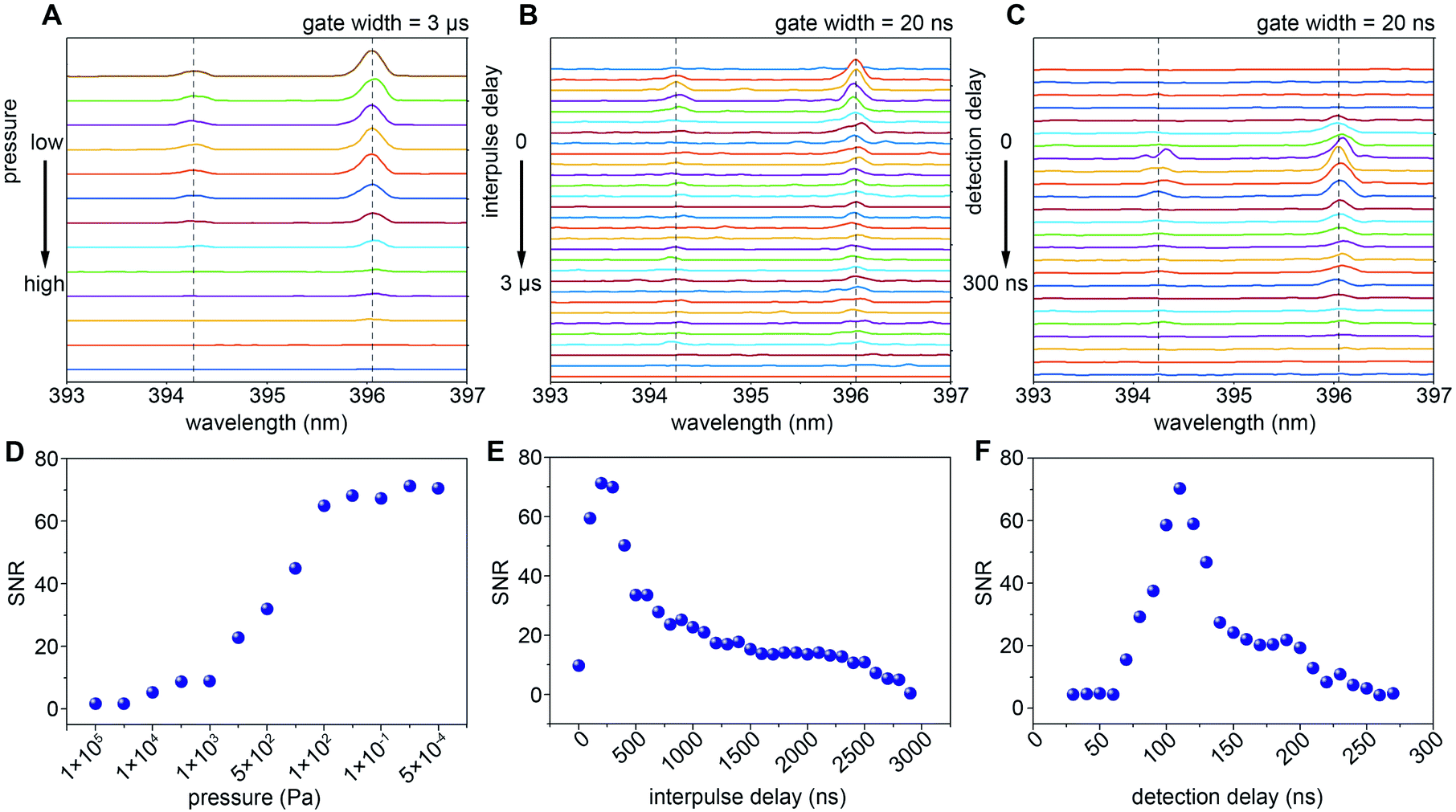 | ||
| Fig. 2 Optimization of gas pressure, interpulse delay and detection delay. The emission spectra of Al(I) at 394.4 nm and 396.1 nm at different pressure (A, from 1 × 10⁵ Pa to 5 × 10⁻⁴ Pa), different interpulse delay (B, from 0 ns to 2900 ns) and different detection delay (C, from 30 ns to 270 ns). The relationships of the signal-to-noise ratio (SNR) of spectral emission of Al(I) at 396.1 nm at different pressure (D), interpulse delay (E) and detection delay (F). | ||
 | ||
| Fig. 3 Spectral emission of Al(I) at 394.4 nm and 396.1 nm from a single laser pulse with single pulse LIBS (A), single laser pulse with double-pulse LIBS (B), and intensity changes with the change of the nanosecond laser energy (C). | ||
3.2 The 500 nm resolution LIBS imaging
Under the above experimental conditions, we carried out the imaging detection on self-made Al mesh samples and a series of digital codes on a SIM chip. To avoid overlap-sampling, the frequency of the laser was set at 10 Hz and the speed of sample movement was set at 5 μm s−1, which means that the distance between the two adjacent sampling spots is 500 nm (pixel size). The nanoscale LIBS imaging results of the two grid samples of different shapes are shown in Fig. 4B and F with imaging areas of 75 × 60 μm2 and 200 × 150 μm2, respectively. Obviously, the Al(I) images at 396.1 nm are highly consistent with the areas of the white aluminum coating pattern captured with a microscope. As Fig. 4C shows, through mathematical statistics of the data in the yellow area of Fig. 4B, LIBS spectral emission signals show high uniformity and stability at different positions on the aluminum coating. The error bars represent the relative standard deviations (RSDs) of the data in vertical directions. By definition, the lateral resolution is considered as the distance between 16% and 84% amplitude change of a line profile representing a sharp edge. By choosing a sharp edge in the red part of Fig. 4C, the imaging resolution is revealed to be approximately 480 nm, which is the level that cannot be achieved by the ordinary LIBS imaging technique. In addition, we have demonstrated the capability of this nanoscale resolution LIBS imaging technology for a SIM chip. As shown in Fig. 4G, the ROI is a series of 3-micron-wide serial numbers on the chip. Its Al image (Fig. 4H) is quite consistent with its optical image.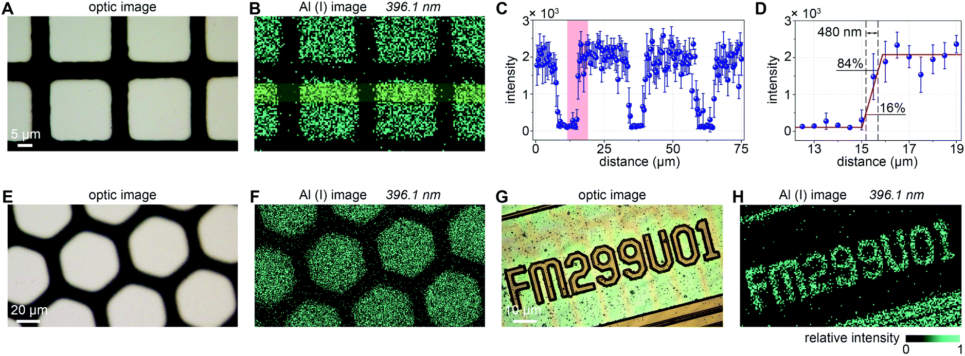 | ||
| Fig. 4 Nanoscale imaging results of Al mesh samples and a series of numbers on the SIM chip. (A and E) Optical image of the imaging area of two different shapes of Al meshes on a silica wafer. (B and F) LIBS imaging of Al(I) at 396.1 nm. (C) Average line-scan profile of the region outlined in (B). (D) Magnified line-scan profile of the marked edge margin in (C). (G) Optical image of the ROI on the chip. (H) Nanoscale LIBS imaging of Al(I) at 396.1 nm. | ||
3.3 Evaluation of limits of detection (LODs)
In the application of nanoscale resolution LIBS imaging, the small sampling amount brings great challenges to the LOD of the technology. We first consider the ALOD and RLOD level of this NLP-based nanoscale LIBS imaging method before more complicated imaging applications. The ALOD experiment is carried out on a smooth indium film. As shown in Fig. 5A, with different laser energy applied to the In film, different sizes of craters can be obtained on the surface of the film, ranging from 400 nm to 1.4 μm in diameter. Fig. 5B displays the spectral emissions of In(I) at 410.2 nm for different sizes of craters, which reveals that a positive correlation between signal intensity and the crater size (ablated amount) can be established. The spectra in Fig. 5B represent the average result of three sets of experiments. It is worth emphasizing that when the femtosecond laser energy is 47 nJ, the sample crater with a diameter of 400 nm can be clearly observed on the surface of the In film, but its steady emission signal cannot be obtained. Through linear fitting, we obtain the relationship between the signal intensity and different ablated amounts (Fig. 5C). The error bars represent the RSDs of the three sets of experiments and indicate the good stability of the NLP-based double-pulse LIBS technique. The 3-fold standard deviation (3σ) value for the spectral emission intensity in the blank spectrum is 79.3; therefore, the ALOD of NLP-based LIBS for In can be calculated from 3σ and the slopes of the calibration curves. Provided that the density of In is about 7.31 g cm−3, the resultant ALOD can be calculated to be 18.3 fg. Fig. 5D shows the profile of the crater obtained under the condition of a femtosecond laser energy of 61 nJ. It can be seen that the diameter of the crater is about 450 nm and the depth is about 100 nm. On the premise of such a small amount of ablation, we made a linear fit through the detection of the In–Sn alloy with different ratios, and obtained the RLOD of In as 0.6% (Fig. 5E and F). It is worth noting that the trend of the relationship between LIBS spectral emission intensity and In concentration might show a slight self-absorption phenomenon in Fig. 5F, which may be caused by the increase of the number of ground states and excited state particles produced by laser interaction with the sample. However, since the vacuum environment can greatly reduce the self-absorption effect, it is not taken into account in the process of linear fitting. | ||
| Fig. 5 Evaluation of the ALOD and RLOD. (A) AFM images of ablated craters on a smooth In film with different femtosecond laser energies. (B) Spectral emission of In(I) at 410.2 nm of the ablated craters of different sizes in (A). (C) Linear fitting of the spectral emission intensity and ablated volume of In. (D) Profile map of the crater on the In film at a laser energy of 61 nJ. (E) Spectral emission of In(I) at 410.2 nm of different proportions of In–Sn alloys. (F) Linear fitting of In spectral emission intensity and different In concentrations from 1% to 50% in the In–Sn alloy. | ||
3.4 Nanoscale LIBS imaging of single cells
Single cell imaging is an important research direction in the field of life science.51,52 At present, fluorescence imaging is the most commonly used single cell imaging method.23 The application of LIBS in tissue imaging has been reported with no fluorescent probe needed,15 but due to the limitations of sensitivity and lateral resolution, the application in single cell imaging is still at a blank stage. Due to biocompatibility, being non-toxic and other advantages, nanoparticles are widely used in life science experiments, such as nanoparticle drug loading, nanoparticle photothermal therapy and so on.53–55 Here, we used the NLP-based double-pulse LIBS imaging technology for the first time to visually detect the subcellular distribution of nanoparticles within a single cell. Mouse mononuclear macrophages leukemia cells and InP nanoparticles are selected for this research objective. The optical images of the cells and fluorescence images of the lysosomes were obtained by using a confocal laser scanning microscope (CLSM). The cells were then freeze-dried and placed on the XY micro-positioner in the sampling area. Fig. 6 shows two groups of the comparative results of LIBS images of In(I) at 410.2 nm and their optical images, with the imaging range of 120 × 90 μm2, respectively. As in the previous experiment, the distance between each sampling point was set to 500 nm. In the CLSM images, the red channel represents the position of the lysosomes. As shown in Fig. 6B and D, nanoscale LIBS imaging results show that the signal of In could be detected in cells, and the In distribution is basically consistent with the location of the lysosomes. Based on the result, we can verify the model of cell–nanoparticle interaction: nanoparticles in aqueous solution enter the cells through endocytosis and reside in the intracellular lysosomes. | ||
| Fig. 6 Nanoscale LIBS imaging of InP nanoparticles within singe cells. (A and C) Optical image of cells stained with LysoTracker Red DND-99. (B and D) LIBS imaging of In(I) at 410.2 nm. | ||
4. Conclusions
In conclusion, an NLP-based double-pulse LIBS imaging technology has been proposed with great operability and reliability. With the enhancement of spectral emission using a double-pulse laser and a novel NLP high-resolution sampling approach, we obtained a signal with a SNR 70× greater than that of single-pulse LIBS when the ablated crater size was less than 500 nm in diameter on an Al film. The relative limits of detection and absolute limits of detection can reach 0.6% and 18.3 fg, respectively, which can be hardly achieved by existing LIBS techniques. Using this method, we visualized the mesh samples and serial numbers on a chip with an imaging resolution of 500 nm. Even more exciting, the location of InP nanoparticles in organelles within single cells can also be clearly and quickly obtained, which is helpful in understanding the interaction between nanomaterials and cells. This strategy presents a nano-scale and sensitive imaging platform for elemental detection, which has great potential in the analysis of nano materials, microstructures, biological tissues and even tiny biological units such as single cells.Conflicts of interest
There are no conflicts to declare.Acknowledgements
The authors gratefully acknowledge the financial support from the Natural Science Foundation of China (21974116, 21521004).References
- D. R. Ifa, N. E. Manicke, A. L. Dill and R. G. Cooks, Science, 2008, 321, 805 CrossRef CAS PubMed.
- L. A. McDonnell and R. M. A. Heeren, Mass Spectrom. Rev., 2007, 26, 606–643 CrossRef CAS PubMed.
- X. Hua, H.-W. Li and Y.-T. Long, Anal. Chem., 2018, 90, 1072–1076 CrossRef CAS PubMed.
- J. Han, X. Huang, H. Liu, J. Wang, C. Xiong and Z. Nie, Chem. Sci., 2019, 10, 10958–10962 RSC.
- L. Jolivet, M. Leprince, S. Moncayo, L. Sorbier, C. P. Lienemann and V. Motto-Ros, Spectrochim. Acta, Part B, 2019, 151, 41–53 CrossRef CAS.
- Q. Lu, Y. Hu, J. Chen and S. Jin, Anal. Chem., 2017, 89, 8238–8243 CrossRef CAS PubMed.
- C. Giesen, H. A. O. Wang, D. Schapiro, N. Zivanovic, A. Jacobs, B. Hattendorf, P. J. Schüffler, D. Grolimund, J. M. Buhmann, S. Brandt, Z. Varga, P. J. Wild, D. Günther and B. Bodenmiller, Nat. Methods, 2014, 11, 417 CrossRef CAS PubMed.
- X. Li, H. Yin, Z. Wang, Y. Fu, Z. Li and W. Ni, Spectrochim. Acta, Part B, 2015, 111, 102–107 CrossRef CAS.
- X. Bai, F. Cao, V. Motto-Ros, Q. Ma, Y. Chen and J. Yu, Spectrochim. Acta, Part B, 2015, 113, 158–166 CrossRef CAS.
- X. Wang, L. Shi, Q. Lin, X. Zhu and Y. Duan, J. Anal. At. Spectrom., 2014, 29, 1098–1104 RSC.
- P. Zheng, H. Liu, J. Wang, B. Yu, B. Zhang, R. Yang and X. Wang, Anal. Methods, 2014, 6, 2163–2169 RSC.
- J. Xiu, S. Zhong, H. Hou, Y. Lu and R. Zheng, Appl. Spectrosc., 2014, 68, 1039–1045 CrossRef CAS PubMed.
- W. Liao, Q. Lin, Y. Xu, E. Yang and Y. Duan, Nanoscale, 2019, 11, 5346–5354 RSC.
- D. Dong, L. Jiao, X. Du and C. Zhao, Chem. Commun., 2017, 53, 4546–4549 RSC.
- Y. Gimenez, B. Busser, F. Trichard, A. Kulesza, J. M. Laurent, V. Zaun, F. Lux, J. M. Benoit, G. Panczer, P. Dugourd, O. Tillement, F. Pelascini, L. Sancey and V. Motto-Ros, Sci. Rep., 2016, 6, 29936 CrossRef CAS PubMed.
- M. Abdelhamid, F. J. Fortes, M. A. Harith and J. J. Laserna, J. Anal. At. Spectrom., 2011, 26, 1445–1450 RSC.
- M. Bonta, J. J. Gonzalez, C. D. Quarles, R. E. Russo, B. Hegedus and A. Limbeck, J. Anal. At. Spectrom., 2016, 31, 252–258 RSC.
- X. Le Guével, M. Henry, V. Motto-Ros, E. Longo, M. I. Montañez, F. Pelascini, O. de La Rochefoucauld, P. Zeitoun, J.-L. Coll, V. Josserand and L. Sancey, Nanoscale, 2018, 10, 18657–18664 RSC.
- R. Stöckle, P. Setz, V. Deckert, T. Lippert, A. Wokaun and R. Zenobi, Anal. Chem., 2001, 73, 1399–1402 CrossRef PubMed.
- D. Kossakovski and J. L. Beauchamp, Anal. Chem., 2000, 72, 4731–4737 CrossRef CAS PubMed.
- V. Zorba, X. Mao and R. E. Russo, Anal. Bioanal. Chem., 2010, 396, 173–180 CrossRef CAS PubMed.
- Z. Liang, S. Zhang, X. Li, T. Wang, Y. Huang, W. Hang, Z. Yang, J. Li and Z. Tian, Sci. Adv., 2017, 3, eaaq1059 CrossRef PubMed.
- Z. Yin, X. Cheng, R. Liu, X. Li, L. Hang, W. Hang, J. Xu, X. Yan, J. Li and Z. Tian, Angew. Chem., Int. Ed., 2019, 58, 4541–4546 CrossRef CAS PubMed.
- D. Menut, P. Fichet, J.-L. Lacour, A. Rivoallan and P. Mauchien, Appl. Opt., 2003, 42, 6063–6071 CrossRef CAS PubMed.
- X. Wang, V. Motto-Ros, G. Panczer, D. De Ligny, J. Yu, J. M. Benoit, J. L. Dussossoy and S. Peuget, Spectrochim. Acta, Part B, 2013, 87, 139–146 CrossRef CAS.
- M. S. Afgan, Z. Hou and Z. Wang, J. Anal. At. Spectrom., 2017, 32, 1905–1915 RSC.
- D. Bäuerle, Laser Processing and Chemistry, Springer Science & Business Media, 2013 Search PubMed.
- P. P. Pronko, S. K. Dutta, D. Du and R. K. Singh, J. Appl. Phys., 1995, 78, 6233–6240 CrossRef CAS.
- H. Hou, L. Cheng, T. Richardson, G. Chen, M. Doeff, R. Zheng, R. Russo and V. Zorba, J. Anal. At. Spectrom., 2015, 30, 2295–2302 RSC.
- M. Wang, L. Jiang, S. Wang, Q. Guo, F. Tian, Z. Chu, J. Zhang, X. Li and Y. Lu, Anal. Chem., 2019, 91, 9952–9961 CrossRef CAS PubMed.
- P. P. Pronko, S. K. Dutta, J. Squier, J. V. Rudd, D. Du and G. Mourou, Opt. Commun., 1995, 114, 106–110 CrossRef CAS.
- Y. Cui, I. V. Veryovkin, M. W. Majeski, D. R. Cavazos and L. Hanley, Anal. Chem., 2015, 87, 367–371 CrossRef CAS PubMed.
- L. Novotny and S. J. Stranick, Annu. Rev. Phys. Chem., 2006, 57, 303–331 CrossRef CAS PubMed.
- Z. Liang, Z. Yin, H. Yang, Y. Xiao, W. Hang and J. Li, TrAC, Trends Anal. Chem., 2016, 75, 24–34 CrossRef CAS.
- N. Abeyasinghe, S. Kumar, K. Sun, J. F. Mansfield, R. Jin and T. Goodson, J. Am. Chem. Soc., 2016, 138, 16299–16307 CrossRef CAS PubMed.
- D. Cleveland and R. G. Michel, Appl. Spectrosc. Rev., 2008, 43, 93–110 CrossRef CAS.
- O. Samek, A. Kurowski, S. Kittel, S. Kukhlevsky and R. Hergenröder, Spectrochim. Acta, Part B, 2005, 60, 1225–1229 CrossRef.
- D. J. Hwang, C. P. Grigoropoulos, J. Yoo and R. E. Russo, Appl. Phys. Lett., 2006, 89, 254101 CrossRef.
- D. J. Hwang, H. Jeon, C. P. Grigoropoulos, J. Yoo and R. E. Russo, J. Appl. Phys., 2008, 104, 013110 CrossRef.
- M. V. Zoriy, M. Kayser and J. S. Becker, Int. J. Mass Spectrom., 2008, 273, 151–155 CrossRef CAS.
- J. S. Becker, A. Gorbunoff, M. Zoriy, A. Izmer and M. Kayser, J. Anal. At. Spectrom., 2006, 21, 19–25 RSC.
- X. Wang, Z. Liang, Y. Meng, T. Wang, W. Hang and B. Huang, Spectrochim. Acta, Part B, 2018, 141, 1–6 CrossRef CAS.
- J. Scaffidi, S. M. Angel and D. A. Cremers, Anal. Chem., 2006, 78, 24–32 CrossRef PubMed.
- D. A. Cremers, L. J. Radziemski and T. R. Loree, Appl. Spectrosc., 1984, 38, 721–729 CrossRef CAS.
- J. Uebbing, J. Brust, W. Sdorra, F. Leis and K. Niemax, Appl. Spectrosc., 1991, 45, 1419–1423 CrossRef CAS.
- Y. Lu, V. Zorba, X. Mao, R. Zheng and R. E. Russo, J. Anal. At. Spectrom., 2013, 28, 743–748 RSC.
- G. Cristoforetti, Spectrochim. Acta, Part B, 2009, 64, 26–34 CrossRef.
- G. Cristoforetti, S. Legnaioli, V. Palleschi, A. Salvetti and E. Tognoni, Spectrochim. Acta, Part B, 2004, 59, 1907–1917 CrossRef.
- A. J. Effenberger Jr and J. R. Scott, Sensors, 2010, 10, 4907–4925 CrossRef PubMed.
- K. Rifai, S. Laville, F. Vidal, M. Sabsabi and M. Chaker, J. Anal. At. Spectrom., 2012, 27, 276–283 RSC.
- R. Zenobi, Science, 2013, 342, 1243259 CrossRef CAS PubMed.
- J. Pisonero, D. Bouzas-Ramos, H. Traub, B. Cappella, C. Álvarez-Llamas, S. Richter, J. C. Mayo, J. M. Costa-Fernandez, N. Bordel and N. Jakubowski, J. Anal. At. Spectrom., 2019, 34, 655–663 RSC.
- E. Hinde, K. Thammasiraphop, H. T. T. Duong, J. Yeow, B. Karagoz, C. Boyer, J. J. Gooding and K. Gaus, Nat. Nanotechnol., 2016, 12, 81 CrossRef PubMed.
- X. Ma, Y. Wu, S. Jin, Y. Tian, X. Zhang, Y. Zhao, L. Yu and X.-J. Liang, ACS Nano, 2011, 5, 8629–8639 CrossRef CAS PubMed.
- Z. Zhao, D. Huang, Z. Yin, X. Chi, X. Wang and J. Gao, J. Mater. Chem., 2012, 22, 15717–15725 RSC.
| This journal is © The Royal Society of Chemistry 2020 |