
 Open Access Article
 This Open Access Article is licensed under a Creative Commons Attribution-Non Commercial 3.0 Unported Licence
Fabrication and evaluation of flexible electrowetting display with support pillars†
Hui
Li
 *a,
Ruihuan
Li
b,
Hongwei
Jiang
b,
Xiaoting
Fang
b,
Xiaozhe
Yin
c and
Rui
Zhou
b
*a,
Ruihuan
Li
b,
Hongwei
Jiang
b,
Xiaoting
Fang
b,
Xiaozhe
Yin
c and
Rui
Zhou
b
aGuangdong Provincial Key Laboratory of Micro/Nano Optomechatronics Engineering, College of Mechatronics and Control Engineering, Shenzhen University, Nanhai Ave 3688, Shenzhen 518060, P. R. China. E-mail: huili@szu.edu.cn
bInstitute of Electronic Paper Displays, South China Academy of Advanced Optoelectronics, South China Normal University, Guangzhou 510006, P. R. China
cInstitute for Advanced Materials, Guangdong Provincial Key Laboratory of Quantum Engineering and Quantum Materials, South China Normal University, Guangzhou 510006, P. R. China
First published on 21st July 2020
Abstract
With the development of portable and wearable devices, flexible displays have attracted extensive interest and have become increasingly important in our daily life. In this study, a flexible electrowetting display (FEWD) was proposed and fabricated. To prevent a short circuit between the top and bottom electrodes, various types of support pillars were fabricated on the top substrates through a photolithography technique. The FEWD was measured under positive and negative bending conditions, with the applied voltage increasing from 0 to 24 V. The aperture ratio and response time were investigated to better evaluate and understand the performance of the FEWD. The mechanical properties of the support pillars and the FEWD were evaluated by means of compression force and cyclic bending tests, respectively. The results showed that the FEWD operated properly at 24 V under a bending curvature of 0.25 cm−1, achieving the largest aperture ratio of 54.96%. Moreover, the oil movement could be influenced by the support pillars in the pixel. With the advantages of both optical performance and flexibility, an FEWD with support pillars is a novel item for future development of reflective transparent displays and provides a promising strategy for developing flexible, wearable, and visible devices.
1. Introduction
With the accelerating development of electronic and wearable displays, reflective and transparent displays, such as reflective liquid crystal displays and electrophoretic displays, are desired as promising and attractive components, and widely employed in daily life.1–3 The electrowetting display (EWD) was first fabricated in 2003 by Hayes and Feenstra at Philips Research Labs,4 and since then, there has been great progress in developing it among other alternatives. Based on the theory of electrowetting on dielectric, the EWD consists of electrodes, conductive liquid, colored oil, hydrophobic layer, and hydrophilic pixel wall, and facilely driven by a suitable applied voltage between the conductive liquid and the electrode underneath. Zhou et al. have described in detail the working principle for the EWD.5 The EWD has potentially presented many significant advantages, including energy savings, steady fabrication process, satisfactory optical performance, fast response for video media, and colorful design,6–8 and thus, it is a highly prospective solution for future displays.It has been expected that the flexible display will play an increasing role in many applications, such as a newspaper-like display, wearable display, and others.9 Despite the major advantages of the EWD described above, there still remain technical challenges with its flexibility in terms of design and fabrication. In general, when voltage is not applied between the top and bottom electrodes, oil spreads over the confined electrowetting pixel. When voltage is applied, the oil contracts to the corner of the pixel. Thus, in order to prevent the oil phase from overflowing from pixels, the present state-of-the-art work mainly employs an EWD fabrication process based on a glass substrate. Wu et al.10 simultaneously coated and patterned fluoropolymer films on indium tin oxide (ITO) glass for an EWD device. Chen et al.11 also successfully fabricated a poly(imide siloxane) hydrophobic insulator layer on ITO glass based on screen-printing technology, and the resulting large-area EWD exhibited good switch performance and relatively high yield. Furthermore, the technological barrier of a glass substrate, instead of a flexible substrate such as polyethylene terephthalate or paper, lies in the difficulty of the temperature limitation during the fabrication process of EWDs because the curing temperature of traditional hydrophobic material is higher than 200 °C.10
Kim and Steckl12 built electrowetting structures, including a metal ground electrode, dielectric layer, and fluoropolymer layer, on Sappi paper. They found that the resulting electrowetting device on paper could attain a contact angle change in ambient oil, with a fast switching time of 20 ms. However, this type of paper substrate merely remained in the stage of electrowetting on dielectric, and has not been used in EWD applications. In order to manufacture a flexible electrowetting display, Hsieh et al.13 inserted a SiNx layer and rough surface into the electrowetting insulator and built a flexible electrowetting display based on a polyethylene terephthalate (PET) substrate. They found that lower saturation voltage could be achieved by changing the surface structure and inserting a dielectric layer, but the bending characteristics of a flexible display were not presented. Above all, challenges still remain for the fabrication and investigation of flexible electrowetting displays.
Based upon the analysis above, in order to enhance the flexibility of an EWD, we disclose the strategy of utilizing support pillars for flexible electrowetting display (FEWD) devices in this study. Polyethylene naphthalate (PEN) with an ITO layer was selected as the substrate, and the support pillars (SUN-1901 photoresist), featured with various pitch distances, were built on the top substrate through the photolithography technique. The related properties of the support pillars, including the surface topography and wettability, were characterized by 3D microscope, atomic force microscopy (AFM), and contact angle analysis. To increase our understanding of the influence of support pillars inside a FEWD and achieve the most optimal optical performance and mechanical properties, it is also necessary to perform investigations to obtain comprehensive information for design optimization. The current study may lead to an increased understanding of support pillars and be important for design and fabrication of novel FEWD devices.
2. Experimental section
2.1 Materials
Polyethylene naphthalate (PEN, purchased from South China Xiangcheng Science and Technology Co.) with an indium tin oxide (ITO) layer, featuring a resistance of 6 Ω □−1, was used as the substrate in this study. Hyflon AD 40HS (purchased from Solvay Co.) was adopted as the hydrophobic insulator. HN-018N and SUN-1901 photoresist were obtained from Suntific Co. for the pixel walls and support pillars, respectively. Potassium hydroxide (KOH) and tetramethyl hydroxide (TMAH) were purchased from Aladdin. Deionized water was obtained from an in-house water purification system (Ultrapure UV, Shanghai Hitech Instruments Co., Ltd., China).2.2 Manufacturing method
Fig. 1(a) shows that a hydrophobic layer and pixel wall were built on the bottom substrate, and colored oil was filled into the pixel. There were support pillars on the surface of the top substrate to prevent short circuits between the two electrodes while the FEWD is being bent. Fig. 1(b) shows the characteristic parameters of a FEWD while being bent, including curvature K and curvature radius R. Moreover, there are two states while the FEWD undergoes bending, positive bending and negative bending. Detailed descriptions are shown in the following section.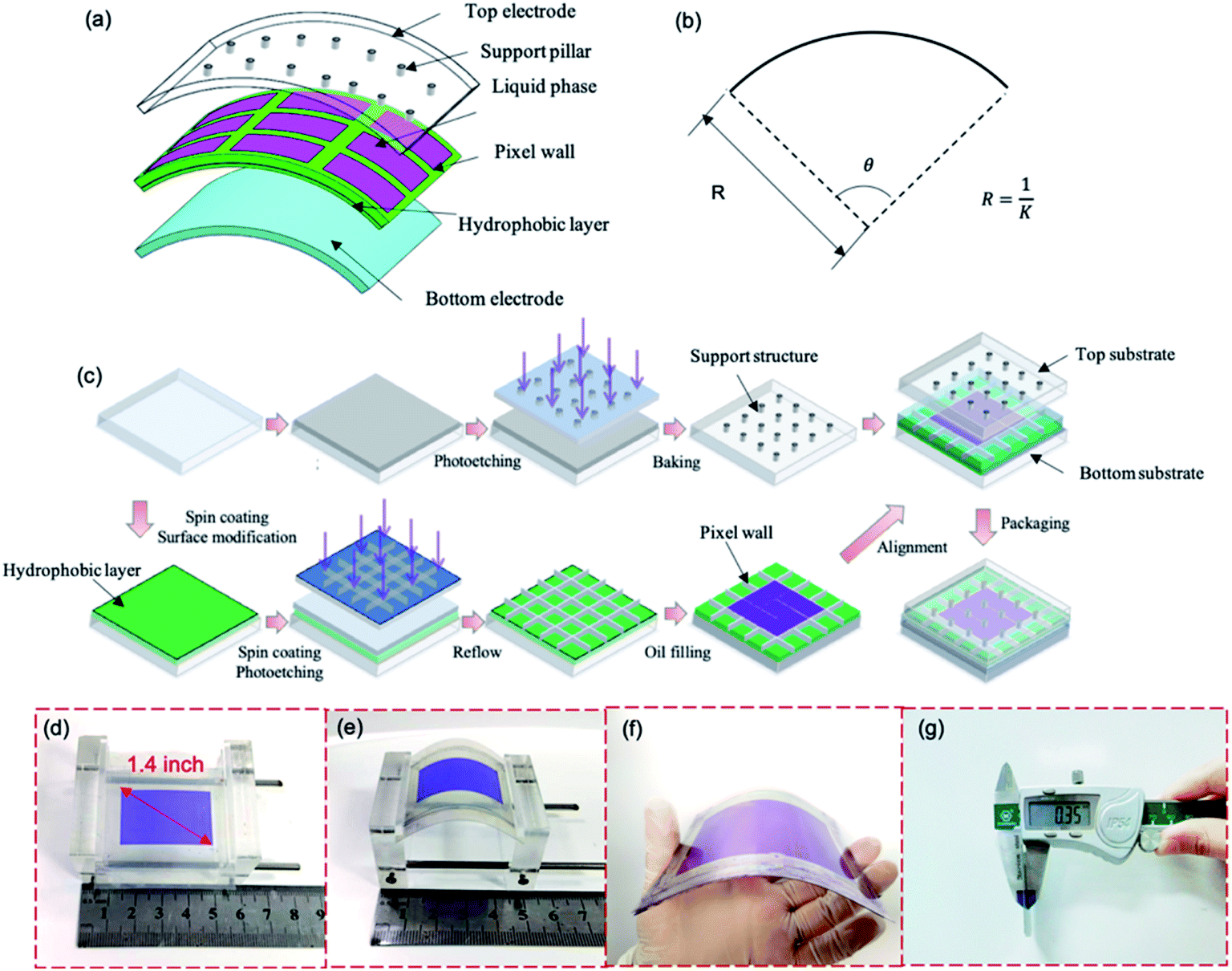 | ||
| Fig. 1 (a) Schematic diagram of the FEWD; (b) characteristic parameters; (c) schematic diagram of the fabrication process; (d) photograph of the FEWD sample with a diagonal of 1.4 inch; (e) flexibility of the FEWD; (f) photograph of the FEWD being bent, with a diagonal length of 4 inch; and (g) thickness of the FEWD. | ||
Fig. 1(c) shows a schematic diagram of the manufacturing process for the FEWD. The entire process mainly consists of three steps: bottom substrate preparation, top substrate preparation, and plate sealing. In detail, the bottom substrate was treated as follows. Initially, the PEN film with an ITO layer was cleaned by ultrasound in ethanol solution for 10 minutes. UV irradiation was used to treat the ITO surface, with a water contact angle less than 10°, as can be seen in Fig. S1(a).† Then, the PEN film was fixed on rigid glass to ensure a level surface. Subsequently, the Hyflon material was spin-coated on the ITO surface, while the thickness was controlled at approximately 800 nm. After precuring on a hot plate (EH20B Lab Tech, China) at 85 °C, the entire bottom plate was cured in a furnace with a higher temperature, so that the fluorocarbon solvent could be evaporated accordingly. Due to the low surface energy of the Hyflon material, it was difficult to coat photoresist on the surface. Thus, plasma was used to modify the wettability of Hyflon so that it was hydrophilic in advance, by means of reactive ion etching equipment (ME-6A, Chinese Academy of Science, China). Next, an HN-018N pixel wall was fabricated on the surface by photolithography. Then, the substrate was heated so that the Hyflon surface would recover the hydrophobic state. The wettability of the Hyflon surface is shown in Fig. S1(b).† In the next step, colored oil was uniformly filled into the pixel through raster filling at low speed (1 mm s−1).
For the top substrate preparation, the PEN substrate was also removed by rinsing. Then, a SUN-1901 photoresist was spin-coated on the surface. Support pillars were fabricated by means of photoetching. To enhance the strength of the support pillars, a curing process was used to completely remove the solvent. Before assembling the two substrates, the top substrate was treated with ozone for 5 min to provide hydrophilic support pillars, as shown in Fig. S1(c).† Finally, these two electrodes were sealed with pressure-sensitive adhesive by an automatic alignment machine.
Fig. 1(d) illustrates the dimensions of the FEWD tested in this study, with a diagonal of 1.4 inch. Fig. 1(e) shows the flexibility of the FEWD, which is compressed by the fixture. The response performance of a 1.4-inch FEWD can be found in Movie S1,† and the color of the FEWD was able to quickly switch in response to being controlled by the applied voltage. The patterned words were clearly seen while the FEWD was bent. Fig. 1(f) shows a photograph of the 4-inch FEWD, which was produced according to the above fabrication process. The dynamic bending process of the 4-inch FEWD is shown in Movie S2.† The thickness of the FEWD is 350 μm, as shown in Fig. 1(g).
2.3 Experimental setup
To evaluate the optical properties and response time of the FEWD, the experimental system consisted of two parts, a test section and a data acquisition system, respectively. For the test section, a moving stage was used to fix the two FEWD edges. During testing, the distance between the two edges was controlled by the moving stage, so that the curvature of the FEWD could be accordingly adjusted. Additionally, a controller was used to accurately maneuver the positions of the moving stage. A wave generator (Agilent 33500B Series, Loveland, CO, USA) was used to provide the applied voltage between the top and bottom electrodes, while the frequency was maintained at approximately 5 Hz. It is noted that the applied voltage was increased from 0 to 24 V, with an interval of 1 V, in this study.For the data acquisition system, two different instruments were used to test the aperture ratio of the pixel and the response time. In general, in order to measure the aperture ratio of the pixel during testing, a high-speed camera (Phantom MiRO M110, Vision Research, USA) together with a microscope (CKX41, Olympus, Japan) was adopted to observe the switching process of pixels and capture the visual images through a computer. The automatic process was driven by LABVIEW software. A lamp was used in this experiment to provide sufficient light for viewing the FEWD under a microscope. A box was used to cover the outside of the test section, and the box was covered with a black cloth as well to reduce the disturbance of external light. The aperture ratio was evaluated by measuring the average white area fraction percentage (ε) in each pixel during a certain applied voltage, which can be expressed as follows,
 | (1) |
In order to measure the response time, an optical colorimeter (Arges 45, Admesy, Ittervoort, The Netherlands) was firmly attached to the upper surface of the FEWD. The optical response curve of the FEWD is shown in Fig. S2.† The luminance sharply increased while voltage was initially applied, and then subsequently steadied, indicating that the pixel was in the switching-on phase. Here, the response time was defined as the time from luminance zero to the time with a luminance of 90%. In Fig. S2,† the response time was 24.77 ms. It should be noted that the experiments were performed in the dark.
2.4 Characterization
The surface structures of the support pillars were measured using a super deep scene microscope (VHX-2000, Keyence). The thickness of the support pillar was measured with a step profiler (Dektak XT, BRUKER, Germany). The 3D morphology of the support pillars was characterized by a 3D profiler (DCM 3D, Leica, and Germany) and a field emission scanning electron microscope (ZEISS Gemini 500, Carl Zeiss). The surface roughness of the top of the support pillar was measured by an atomic force microscope (Asylum Research MPF-3D). The wettability of the materials used in this study was measured by a contact angle measurement instrument in an ambient environment.3. Results and discussion
3.1 Optical performance of the FEWD
Fig. 2 shows the basic optical performance of the FEWD with a pitch distance of 510 μm. As can be seen in Fig. 2(a), the aperture ratios of the pixels were measured at various voltages under different radii of curvature. As the curvature changed from −0.25 to 0.25 cm−1, and the aperture ratio of the pixels exhibited a gradual upward trend. In particular, the FEWD with the curvature of 0.25 cm−1 had the largest aperture ratio of 54.96% when the applied voltage was 24 V. This result is consistent with the findings of Dou et al.,5 who also found that the aperture ratio of an EWD could reach approximately 50%. Additionally, it was found that an FEWD in a positive bending state exhibited a higher aperture ratio than that in a negative bending state. This phenomenon may be attributed to the difference in the thickness of the oil film. For the positive bending state, there was additional distance at the top of the pixel wall, resulting in the thinning of the oil film, as can be seen in Fig. 2(e). Thus, as the voltage applied on the oil phase increased, the voltage on the water and Hyflon layer correspondingly decreased based on the principle of voltage distribution. Then, the Hyflon surface became hydrophilic according to the Young–Lippmann equation, which can be expressed as, | (2) |
 | ||
| Fig. 2 Optical performance of a FEWD with a pitch distance of 510 μm. (a) Aperture ratios under various curvature radii; (b) aperture ratios under various applied voltages; (c) response time for devices with various curvature radii; (d) response time under various applied voltages; (e) schematic diagrams showing the positive and negative bending states; (f) magnified pixels under the operation voltages of 14–20 V. The device started to illustrate the “on” state at 16 V. | ||
The aperture ratio is also influenced by the applied voltage, as can be seen in Fig. 2(b). When the applied voltage ranged from 16–24 V, there was a good linear relationship between the voltage and the aperture ratio. The higher the applied voltage, the larger the aperture ratio that can be attained. This result is reasonable and can also be explained according to eqn (2). Under a certain curvature, when the applied voltage between the electrodes is increased, the voltage on the Hyflon layer subsequently increases. Hence, the contact angle between the Hyflon surface and water becomes larger, which leads to the increase in the aperture ratio.
The bending characteristics of the FEWD device also present great importance for the switching-on response time of the pixel. Fig. 2(c) shows the relationship between the curvature of the FEWD device and response time. Generally, the measured response time shows a slightly downward trend with increasing curvature. For instance, when the curvature is −0.25 cm−1, the response time of the pixel is 63.45 ms at 16 V voltage, followed by the times of 62.63, 61.56, 60.44, 59.39, and 58.66 ms. Similarly, it is worth noting that the response time is significantly dominated by applied voltage. For the larger curvature, the voltage is relatively higher on the hydrophobic Hyflon layer, in accordance with the explanation given in the above section, resulting in a higher moving velocity for the interface of the phase contact line.14 It is faster for FEWD devices with a larger curvature to achieve a steady state as compared to those with a smaller curvature. As can be seen in Fig. 2(d), it is also expected that the response time will quickly decrease with increasing voltage. In comparison, Dou et al.5 also tested the starting performance for an EWD, but the response time was approximately 33.7 ms, which is approximately equal to the results in our study (t = 36.65 ms for curvature 0). Two reasons may contribute to the above phenomenon in the measurement. First, the hydrophobic material used in their study was AF 1600X, which possesses slightly different dielectric properties as compared to the Hyflon material. Second, the thermal reflow temperature used in our study was approximately 165 °C, which is lower than the conventional temperature. Therefore, the hydrophilic performance is relatively degraded for the movement of a liquid phase, and the response time is longer.
Fig. 2(f) shows magnified optical microscope images of FEWD devices. The voltage varies from 14 to 24 V. When the voltage is 14 V, the pixel is fully occupied by the oil phase. However, the oil film is pushed aside as the voltage rises to 16 V. Then, the aperture ratio continuously increases with the growth of the applied voltage of 16–24 V.
3.2 Characterization of the support pillars
As one of the most important components in a FEWD, the support pillars exert a significant influence on the flexibility. To reveal the microscopic mechanism, the 3D features and surface topography of the support pillars were analyzed. Microscope photographs are shown in Fig. 3(a), (b) and (c), indicating pitch distances of 170, 340 and 510 μm, respectively. The larger the distance, the less the intensity of the support pillars. Fig. 3 also illustrates the 3D structures of the support pillars. The heights of the support pillars were nearly the same for all samples, at approximately 35 μm, as shown in Fig. 3(d). The corresponding surface roughness of the top of a support pillar is shown in Fig. 3(e), which can achieve approximately 23 nm. A scanning electron microscopy (SEM) image of the fabricated support pillars is shown in Fig. S3,† with a pitch distance of 170 μm and diameter of approximately 30 μm.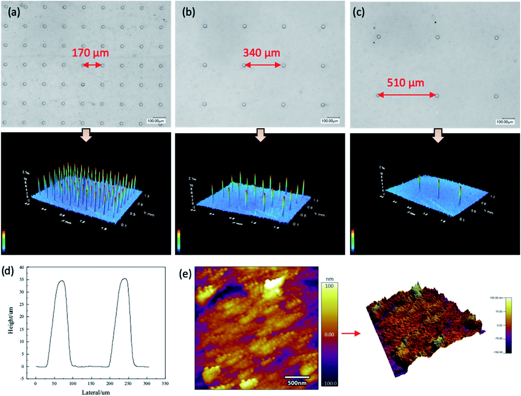 | ||
| Fig. 3 Characterization of the fabricated support pillars with various pitch distances. Microscope photographs and 3D surface profiles for support pillars with (a) p = 170 μm, (b) p = 340 μm, and (c) p = 510 μm (“p” is the distance between two adjacent pillars). (d) Height of the support pillar. (e) AFM images of the top surface of the support pillars. | ||
Two types of support pillar locations are shown to evaluate the effect of the support pillars on oil motion. One type is the support pillars inside the pixel area, and the other type is the support pillars on the pixel wall, as can be seen in Fig. 4. It should be noted that the size of the pixel area is 170 × 170 μm2. Fig. 4(a) illustrates the switching-on state for support pillars located inside the pixel area, and shows that a water phase occupies the area beside the support pillars, once the applied voltage is large enough to drive the liquid. This can be attributed to the fact that the wettability of the support pillar is hydrophilic after the ozone treatment. Then, water would flow along the wall of the support pillar, while the oil moves to the opposite direction. It was also found that if there were no support pillars in the pixel area, the oil motion exhibited random phenomena. However, when the support pillars are on the pixel wall, the phenomenon for oil motion is totally different, as can be seen in Fig. 4(e). When the FEWD is bent at this moment, the support pillars make direct contact with the pixel wall, and merely prevent contact between the two electrodes. The oil motion cannot be influenced, and the directions of the pixel openings are random as well, as can be seen in Fig. 4(f)–(h). Therefore, the support pillars are beneficial for the regular movement of the oil phase in the pixel.
 | ||
| Fig. 4 (a) Schematic diagrams of relative locations of support pillars in the pixel. Effect of support pillars for oil movement, with (b) p = 170 μm, (c) p = 340 μm, and (d) p = 510 μm. (e) Schematic diagrams of relative locations of support pillars on the pixel wall, with (f) p = 170 μm, (g) p = 340 μm, and (h) p = 510 μm. | ||
3.3 Mechanical properties of the FEWD
The mechanical properties of the support pillars were tested, and Fig. 5(a) shows that the strength was evaluated by applying compression force on the support pillars. The radius of the loading head was 0.25 mm, while the loading force was controlled within 60 N. Fig. 5(b) shows microscope photographs of support pillars before and after the force loading. Two types of failure modes for support pillars occurred, consisting of falling off and flattening. When the pitch distance of the support pillars was larger (510 μm), the pillars were more likely to be destroyed. | ||
| Fig. 5 (a) Schematic diagram of the experimental setup to measure the strength of the support pillars. (b) Microscope photographs of the support pillars before and after the application of 40 N loading force. (c) The response time of the FEWD devices that underwent repetitive bending for different numbers of repetitions. Capacitance of FEWD devices that were repetitively bent with differing repetitions: (d) n = 0, (e) n = 100, (f) n = 300. (“n” denotes the number of times that the FEWD was bent). Capacitance of FEWD devices with different curvatures after being bent 100 times, (g) K = 0.17 cm−1, (h) K = 0.2 cm−1, (i) K = 0.25 cm−1. | ||
As a flexible device, the ability to withstand repetitive bending is of importance for the mechanical properties of the FEWD. To evaluate the influence of bending behavior, the response time and capacitance of the FEWD after a cyclic bending test were measured and compared. Fig. 5(c) shows that while the number of bending repetitions ranged from 100 to 400, it is expected that the response time of the FEWD will also increase between 59 ms and 65 ms.
Fig. 5(d) shows the capacitance of the FEWD before bending. When the applied voltage was varied from 0 to 20 V, the capacitance curves for all three different pitch distances were nearly maintained at the same value (4000 pF). With 100 bending repetitions, the capacitance curves were almost at a constant level. However, with 300 repetitions, there was a clear difference in the various support pillars. The capacitance curves for FEWD with pitch distances of 510 μm and 340 μm clearly increase.
Two reasons may contribute to the above tendency. First, because the base PET substrate is a flexible material, small deformations may occur in the area between two support pillars. In other words, the distance between the top and bottom electrode is decreased, which causes increased capacitance. Second, it may be inferred that the bending behavior causes damage to the dielectric layer. In comparison, support pillars with smaller pitch distance can effectively prevent deformation of the FEWD device during bending, thus reducing the risk of physical damage to the dielectric layer.
Fig. 5(g)–(i) show the capacitance of FEWDs with different curvatures, that were repetitively bent 100 times. When the curvature gradually increased from 0 to 0.25 cm−1, there was little change in the capacitance of the FEWD with a pitch distance of 170 μm. However, there were obvious fluctuations for the other two types of FEWDs. This is reasonable because the dielectric layer is forced to be deformed during the bending process, which may influence the distance between the two electrodes. In addition, it is interesting that in Fig. 5(h) and (i), the capacitance curve for the FEWD with a 510 μm pitch distance gradually increases during testing. The possible reason for this may be that there are small cracks on the dielectric film during the cyclic bending test that would affect the stability.
4. Conclusions
In this study, we present the methodology for fabricating a flexible, transparent electrowetting display. It was vital to create support pillars so that the FEWD could bend. These support pillars were built on top of a substrate through photoetching technology, and measured with AFM, SEM, and a 3D profiler. Three different pitches of the pillars were conducted, and the effect on the oil motion was examined. The electro-optical response performance of the FEWD in the bent state was evaluated based on experiments. The mechanical properties of the support pillars were measured and analyzed as well. The main conclusions can be summarized as follows. The aperture ratio increased with increased bending curvature, and it reached the largest aperture ratio of 54.96% with the applied voltage of 24 V at a curvature of 0.25 cm−1. The response time of the FEWD evidently decreased with increasing voltage. The time also showed a downward trend when the bending curvature increased. This phenomenon was attributed to the change in the thickness of the oil film. The resulting voltage change on the insulator surface led to the variation of the contact angle between the insulator surface and the water phase during the electrowetting process. The oil motion direction in the pixel could be effectively and accurately driven according to the support structures. However, when the support pillars made contact with the pixel walls during the bending process, the oil would be randomly pushed away. This is greatly due to the fact that the surface of the support pillar was adequately hydrophilic after the ozone treatment. The mechanical properties of the support pillars were evaluated as well. Falling off and flattening were the two common pillar failure modes after the compression test. After the cyclic bending test, the response speed of the FEWD slowed, and the capacitance would be correspondingly affected.Further studies should be conducted to optimize the performance of the FEWD with support pillars. Further research is still necessary to investigate the effect of the support pillars (e.g., geometry, pitch) and manufacturing parameters (e.g., ozone treatment, curing temperature) for future industrial applications.
Conflicts of interest
We declare that we have no financial and personal relationships with other people or organizations that can inappropriately influence our work. There is no professional or personal interest of any nature or kind in any product, service, and/or company.Acknowledgements
The authors gratefully acknowledge the project support provided by the Natural Science Foundation of Shenzhen University (No. 2110277), China Postdoctoral Science Foundation (No. 2018M640797), and the Natural Science Foundation of Guangdong Province (No. 2019A1515110936).References
- X. Meng, T. Wen, L. Qiang, J. Ren and F. Tang, ACS Appl. Mater. Interfaces, 2013, 5, 3638–3642 CrossRef CAS PubMed.
- L. He, J. Ye, M. Shuai, Z. Zhu, X. Zhou, Y. Wang, Y. Li, Z. Su, H. Zhang and Y. Chen, Nanoscale, 2015, 7, 1616–1622 RSC.
- Y. Zhang, B. Zhen, S. A. S. Al-Shuja'a, G. Zhou, X. Li and Y. Feng, Dyes Pigm., 2018, 148, 270–275 CrossRef CAS.
- R. A. Hayes and B. J. Feenstra, Nature, 2003, 425, 383–385 CrossRef CAS PubMed.
- Y. Dou, B. Tang, J. Groenewold, F. Li, Q. Yue, R. Zhou, H. Li, L. Shui, A. Henzen and G. Zhou, Sensors, 2018, 18, 1114 CrossRef PubMed.
- P. T. C. Lee, C.-W. Chiu, T.-M. Lee, T.-Y. Chang, M.-T. Wu, W.-Y. Cheng, S.-W. Kuo and J.-J. Lin, ACS Appl. Mater. Interfaces, 2013, 5, 5914–5920 CrossRef CAS PubMed.
- T. He, M. Jin, J. C. Eijkel, G. Zhou and L. Shui, Biomicrofluidics, 2016, 10, 011908 CrossRef PubMed.
- J. Heikenfeld, K. Zhou, E. Kreit, B. Raj, S. Yang, B. Sun, A. Milarcik, L. Clapp and R. Schwartz, Nat. Photonics, 2009, 3, 292 CrossRef CAS.
- H.-J. Kwon, H. Shim, S. Kim, W. Choi, Y. Chun, I. Kee and S. Lee, Appl. Phys. Lett., 2011, 98, 151904 CrossRef.
- H. Wu, B. Tang, R. Hayes, Y. Dou, Y. Guo, H. Jiang and G. Zhou, Materials, 2016, 9, 707 CrossRef PubMed.
- X. Chen, T. He, H. Jiang, B. Wei, G. Chen, X. Fang, M. Jin, R. A. Hayes, G. Zhou and L. Shui, Displays, 2015, 37, 79–85 CrossRef CAS.
- D. Y. Kim and A. J. Steckl, ACS Appl. Mater. Interfaces, 2010, 2, 3318–3323 CrossRef CAS PubMed.
- I. Hsieh, L. Chen, H. Chen, K. Lu, J. Cheng and J. Cyue, Low Driving Voltage of Electrowetting Display on Flexible Substrate, 2008 Flexible Electronics and Displays Conference and Exhibition, Phoenix, AZ, 2008, pp. 1–5, DOI:10.1109/FEDC.2008.4483877.
- B. Tang, J. Groenewold, M. Zhou, R. A. Hayes and G. G. Zhou, Sci. Rep., 2016, 6, 26593 CrossRef CAS PubMed.
Footnote |
| † Electronic supplementary information (ESI) available. See DOI: 10.1039/d0na00355g |
| This journal is © The Royal Society of Chemistry 2020 |