DOI:
10.1039/D0NA00318B
(Paper)
Nanoscale Adv., 2020,
2, 4785-4797
Boosting the performance of NO2 gas sensors based on n–n type mesoporous ZnO@In2O3 heterojunction nanowires: in situ conducting probe atomic force microscopic elucidation of room temperature local electron transport†
Received
23rd April 2020
, Accepted 10th August 2020
First published on 12th August 2020
Abstract
Herein, n–n type one dimensional ZnO@In2O3 heterojunction nanowires have been developed and their local electron transport properties during trace-level NO2 gas sensing process have been probed at room-temperature using conducting probe atomic microscopy. Solvothermally synthesized 1D ZnO@In2O3 heterojunction nanowires have been characterized by various spectroscopic and microscopic techniques, which revealed the mesoporous structure indicating their enhanced sensing properties. The dangling bonds and fraction of metal ions to oxygen ions existing on the exposed crystal facets of the heterojunction nanowires have been visualized by employing crystallographic simulations with TEM analysis, which aided in forecasting the nature of surface adsorption of NO2 gas species. In situ electrical characteristics and Scanning Spreading Resistance Microscopic (SSRM) imaging of single ZnO@In2O3 heterojunction nanowires revealed the local charge transport properties in n–n type ZnO@In2O3 heterojunction nanowires. Moreover, the ZnO@In2O3 heterojunction nanowires based sensor exhibited excellent sensitivity (S = 274%), a fast response (4–6 s) and high selectivity towards trace-level concentration (500 ppb) of NO2 gas under ambient conditions with low power consumption. Spatially resolved surface potential (SP) variations in ZnO@In2O3 heterojunction nanowires have been visualized using in situ Scanning Kelvin Probe Force Microscopy (SKPM) under NO2 gas environment at room temperature, which was further correlated with its energy band structure. The work functions of the material evaluated by SKPM reveal considerable changes in the energy band structure owing to the local electron transport between ZnO and In2O3 at the heterojunctions upon exposure to NO2 gas indicating the charge carrier recombination. A plausible mechanism has been proposed based on the experimental evidences. The results suggest that new insights into complex sensing mechanisms deduced from the present investigation on n–n type MOS based heterojunction nanowires under ambient conditions can pave the way for the novel design and development of affordable and superior real-time gas sensors.
Introduction
Among various environmental pollutants released from industrial and automobile emissions, NO2 is considered as the most dangerous air pollutant, as it leads to serious health hazards, and plays a major role in depletion of ozone (O3) and acid rains.1 Hence, it is highly essential to detect trace level NO2 gas for environmental monitoring, human health and safety.2 To address these serious concerns, incredible attempts have been focused on advancement of NO2 gas sensors based on metal-oxide semiconductors (MOSs). ZnO,3 Co3O4,4 SnO2,5 WO3,6 NiO,7 In2O3,8etc. have attracted tremendous interest in the gas sensor sector owing to their inexpensiveness, simple fabrication and superior sensing performance. Among various MOS materials, ZnO and In2O3 possess wider band gaps and have been realized for variety of applications, including gas sensors, solar cells,9 transparent conducting oxides10etc. ZnO having a hexagonal crystal plane arrangement with a wurtzite structure along with a huge exciton binding energy of 60 meV is considered to be an ideal semiconductor for NO2 gas sensors.11–13 However, though ZnO is being used in conventional MOS gas sensors, the issues associated with poor selectivity, high operating temperature and reliability hinder its practical applications. Similarly, n-type In2O3 (rhombohedral structure) has also gained significant attention towards NO2 detection owing to its unique characteristics such as an extensive energy gap (2.5–3.75 eV), high electrical conductivity etc.14 However, pristine ZnO and In2O3 based sensors have found limited practical applicability due to their adverse effects in selectivity, higher operating temperature and poor response at trace level gas concentrations. Numerous studies have attempted to improve their sensing properties by modification with noble metals, surface alteration and shaping with p–n or n–n heterojunctions with alternate MOSs. Mostly, binary oxide heterojunctions formed at the interfaces found to play an important role in augmenting sensing properties. The formation of n–n heterojunctions induces synergistic effects due to coupling of binary oxides with a minimal difference in work functions. Until now, n–n type binary oxide MOS nanohybrids, such as ZnO/SnO2,15 WO3/ZnO,16 WO3/In2O3,17 TiO2/ZnO,18etc. have shown the significance of hetero-interfaces towards detection of noxious NO2. In this scenario, hierarchical hetero-nanostructures with a unique combination of ZnO and In2O3 could be expected to exhibit excellent NO2 gas sensing properties with easy fabrication, long-term stability and enhanced sensitivity.3,19 However, the design of such heterojunction MOS based gas sensors demands precise understanding of the complex sensing mechanism for suitably deploying them for real time applications. Although there are a number of existing reports describing the sensing mechanism of pristine MOSs, there is a serious lack of systematic investigations on heterojunction metal oxide materials owing to their interfacial structural complexity. Based on the literature, it can be ascertained that the development of high aspect ratio, one-dimensional MOS heterojunction nanostructures can greatly influence the sensing properties such as the gas response, sensitivity and selectivity.20,21 Advancements of n–n type MOS heterojunctions could be an appropriate strategy to extend the execution of gas sensors, but, comprehensive investigations pertaining to the complex sensing mechanisms are still under the infancy stage. Also, the crystallographic dependency of dissimilar heterojunction MOS materials on their gas sensor performance has not yet been thoroughly discussed.
Operando and in situ techniques, based on DRIFT,7,19 Raman spectroscopy,22 photoluminescence spectroscopy,23 XPS,24,25 UV-DRS,26 EPR,27etc. have been utilized to elucidate the sensing mechanism of pristine MOSs towards different gases. Recently, Patsha et. al., reported local electron transfer process and surface band bending during methane sensing by pristine GaN nanowires using in situ SKPM analysis.28 Kaur et. al., attempted to explore the charge transfer mechanism of a polypyrrole–tin oxide nanocomposite (PPy–SnO2) nanowire based NH3 sensor using in situ SKPM studies.29 But, so far, no reports are available on exploration of complex sensing mechanism of MOS based heterojunction materials using in situ/operando studies.
Our previous report demonstrated the enhanced NO2 sensing and electron transport properties of n–p type ultra-long ZnO@Bi2O3 heterojunction nanorods.32 Though the ultra-long ZnO based n–p type ZnO@Bi2O3 heterojunction nanorods showed superior NO2 sensing performances, the high operating temperature limited their possible practical applications. With this investigation, we have developed n–n type ZnO@In2O3 heterojunction nanowires, which can operate at reduced operating temperature with sustainable sensitivity. The surface activity of ZnO could be enhanced by coalescence of In2O3 nanoislands on the surface that can act as a lever of charge transfer during exposure of NO2 gas and aided in the augmentation of sensing characteristics. So far, very few reports have attempted SKPM to demonstrate the sensing behaviour of nanomaterials.28–31 To the best of our knowledge, this is the first report on room-temperature local charge transport properties for unravelling the complex mechanism pertaining to NO2 sensing properties of mesoporous n–n type ZnO@In2O3 heterojunction nanowires based on SKPM and SSRM. The NO2 sensing properties of pristine ZnO nanowires and ZnO@In2O3 heterojunction nanowires were investigated towards trace level NO2 gas, and ZnO@In2O3 heterojunction nanowires exhibited excellent sensitivity, improved selectivity and rapid response and recovery time at room temperature, indicating their potential usage in real time applications.
Experimental section
Materials used
Zinc chloride dihydrate (ZnCl2·2H2O, 99.8%, Merck), indium acetate (In(CH3CO2)3, 99.99%, Sigma Aldrich), sodium dodecylbenzene sulfonate (SDS, 99.97%, Merck), sodium carbonate (Na2CO3, 99.9%, Merck), ethylene glycol (EG, 99.8%, Merck), and ethanol (C2H5OH, 99%, Merck) were used without any further purification.
Synthesis of porous ZnO@In2O3 heterojunction nanowires
Porous ZnO nanowires were chemically synthesized by simple hydrothermal method as per our previous reports.32,33 In this investigation, n–n type ZnO@In2O3 heterojunction nanowires were synthesized by solvothermal process. Briefly, 0.5 mM of In(CH3COO)3·xH2O was dissolved in a binary solvent consisting of 1![[thin space (1/6-em)]](https://www.rsc.org/images/entities/char_2009.gif) :3 fraction of ethylene glycol and ethanol followed by 40 min of vigorous stirring. Meanwhile, the surface treatment of 200 mg of ZnO nanowires was carried out using UV-irradiation (254 nm) for 2 min. The above solution was ultrasonicated for 30 min in order to form a homogenous solution. Further, the solution was subjected to heat treatment at 160 °C for 4 h after shifting to a Teflon-sealed SS autoclave of 100 mL capacity. The resultant product was collected; washed and centrifuged several times with 80% ethanol and deionized water to remove the unwanted In2O3 impurities. The product was dried overnight in a hot air oven at 90 °C. The ensuing amorphous precipitate was heat treated for 3 h at 550 °C in air at a ramp rate of 5 °C min−1. After the annealing process, the color of the product turned to light yellow, indicating the crystallization of In2O3 nanoislands on the ZnO nanowires.
:3 fraction of ethylene glycol and ethanol followed by 40 min of vigorous stirring. Meanwhile, the surface treatment of 200 mg of ZnO nanowires was carried out using UV-irradiation (254 nm) for 2 min. The above solution was ultrasonicated for 30 min in order to form a homogenous solution. Further, the solution was subjected to heat treatment at 160 °C for 4 h after shifting to a Teflon-sealed SS autoclave of 100 mL capacity. The resultant product was collected; washed and centrifuged several times with 80% ethanol and deionized water to remove the unwanted In2O3 impurities. The product was dried overnight in a hot air oven at 90 °C. The ensuing amorphous precipitate was heat treated for 3 h at 550 °C in air at a ramp rate of 5 °C min−1. After the annealing process, the color of the product turned to light yellow, indicating the crystallization of In2O3 nanoislands on the ZnO nanowires.
Results and discussion
Mesoporous ZnO nanowires were chemically synthesized via a simple hydrothermal technique.34Scheme 1 illustrates the formation mechanism of In2O3 nanoislands on ZnO nanowires formed in situ using In(CH3COO)3 as the precursor. The chemical reactions during the formation of heterojunction ZnO@In2O3 nanowires can be represented as per eqn (1–3). The purified UV-irradiated ZnO nanowires possess more surface active sites and in the binary solvent of ethanol and ethylene glycol, In3+ gets effectively adsorbed over the surface of ZnO nanowires through hydrogen bonding. During the solvothermal hydrolysis process, the In2O3 nanoislands were firmly anchored over the surface of ZnO nanowires by initially forming a relatively stable complex (indium ethylene glycolate) due to the strong coordination between indium ions and surface active functional groups of ZnO nanowires. The solvothermal process with the aid of pressure and temperature inevitably induces Ostwald ripening that causes the self-organization of In2O3 nanoislands on the surface of ZnO nanowires.35 The resultant mesoporous ZnO@In2O3 heterojunction nanowires were found to be amorphous in nature. The material was further subjected to a high temperature (550 °C) annealing process under oxygen atmosphere in order to improve the crystallinity, and the white powder turned pale yellow.| | | 2In(CH3COO)3 + 3HOCH2CH2OH + 6C2H5OH → In2(OCH2CH2O)3 + (CH3COCH2CH2)3 + H2O | (1) |
| | | ZnO NWs(UV treated) + In2(OCH2CH2O)3 + H2O → ZnO NWs(UV treated) + In2O3 + 3HOCH2CH2OH | (2) |
| |  | (3) |
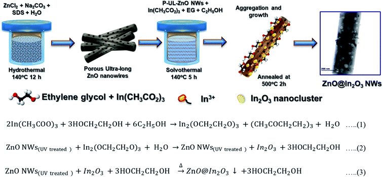 |
| | Scheme 1 Schematic diagram of the synthesis method adopted for n–n type ZnO@In2O3 heterojunction nanowires. | |
Structural and morphological characterization of mesoporous ZnO@In2O3 heterojunction nanowires
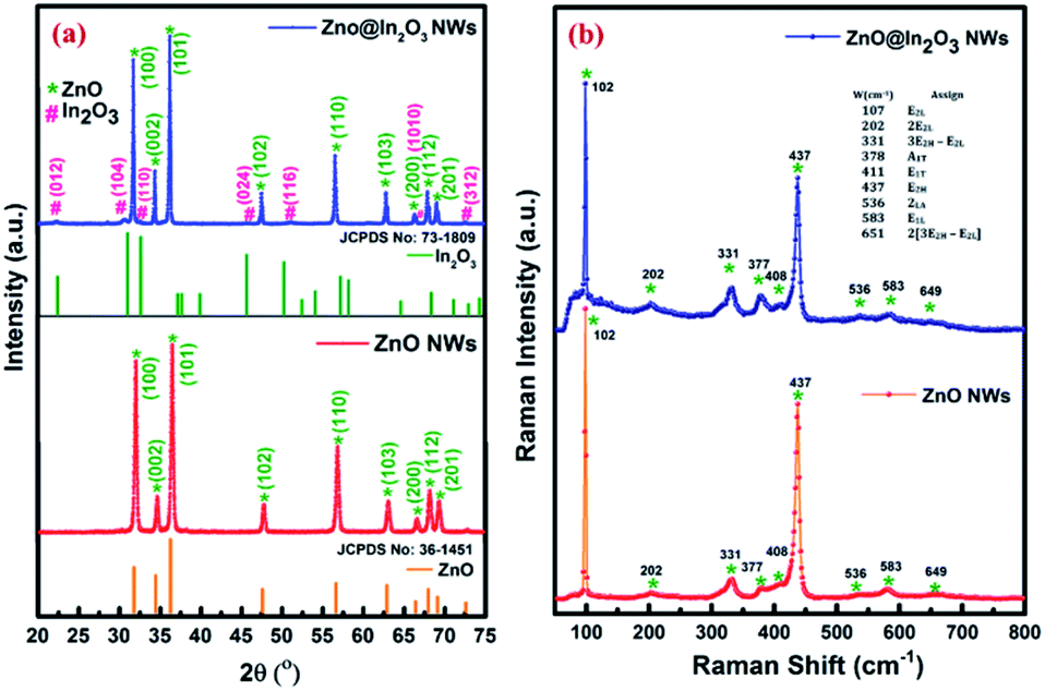
Fig. 1(a) shows the XRD patterns of thermal treated ZnO nanowires and ZnO@In2O3 heterojunction nanowires. The highly intense peaks observed at various diffraction angles (2θ) of 32.03°, 34.79°, 36.43°, 47.69°, 56.74°, 63.15°, 68.07° and 69.20° correspond to the crystal planes (100), (002), (101), (110), (103), (200), (112) and (201) of ZnO. The respective peaks matching the hexagonal wurtzite crystal structure of ZnO were indexed (JCPDS card no. 36-1451), with lattice parameters of a = 3.249 Å and c = 5.206 Å. The absence of additional peaks clearly confirms the purity of ZnO nanowires. The calculated fraction of intensity among the (101) and (100) planes (I100/I101) of the ZnO nanowires was found to be higher than that of pristine ZnO which evidentially reflected in the preferential growth of ZnO nanowires along the 〈100〉 direction. In addition to the ZnO peaks (hexagonal wurtzite structure), the ZnO@In2O3 nanowires also showed peaks at 22.33°, 30.97°, 32.59°, 45.57°, 52.41°, and 72.84° which are attributed to the lattice planes of (012), (104), (110), (024), (116) and (312) of the rhombohedral In2O3 crystal structure (JCPDS no. #73-1809), suggesting the formation of heterojunctions.36
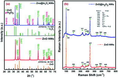 |
| | Fig. 1 (a) XRD patterns and (b) Raman spectra of ZnO nanowires and ZnO@In2O3 heterojunction nanowires. | |
Fig. 1(b) presents the room-temperature Raman peak shifts observed for ZnO nanowires and ZnO@In2O3 heterojunction nanowires using the excitation wavelength of a 532 nm laser source in the backscattering mode. The Raman spectral analysis of ZnO nanowires showed an intense peak at 438 cm−1 confirming the hexagonal wurtzite structure, which corresponds to the E2 high mode of ZnO. Furthermore, the peaks that appeared at the lower frequency range of 329 cm−1 and 378 cm−1 are related to the zone edging phonon vibrations, E2 high − E2 low and A1(TO), respectively.37 A wide peak observed at 583 cm−1 assigned to E1(LO) confirms the presence of more oxygen vacancies (Vo) and zinc interstitials (Zni). The considerable shifts noticed for the ZnO@In2O3 heterojunction nanowires could be due to the charge transfer at the interfaces of In2O3 nanoislands grown on the ZnO nanowires. The overall peak intensity was found to be suppressed due to the growth pattern of In2O3 nanoislands formed over the ZnO nanowires. The peak related to the E1 (LO) mode of ZnO was suppressed due to the presence of interstitial defects, which acted as favorable sites for the growth of In2O3 nanoislands. The peak related to the E2 (high) mode was found to be wide and weak, same as that observed in the amorphous phase, which might be due to the formation of heterojunctions between Zn–O and In–O bonds. The fading of the A1(LO) mode at 583 cm−1 is because of the existence of zinc interstitials, oxygen vacancy states, etc.38
The HRTEM images of pristine porous ZnO nanowires and porous ZnO@In2O3 heterojunction nanowires are shown in Fig. 2 and S2.† The In2O3 nanoislands were found to be evenly anchored over the ZnO nanowires with a mean particle size of 12 ± 0.25 nm which confirmed the formation of ZnO–In2O3 interfaces (Fig. 2(a)). HRTEM analysis of the hybrid nanowires revealed a well-resolved inter-planar spacing related to ZnO with d(002) = 2.67 Å and In2O3 with d(110) = 2.73 Å. Though HRTEM of ZnO and In2O3 indicated the exposed planes, such as (002) and (110) respectively, it should be noted that the interplanar distance between the (002) plane of ZnO and the (110) plane of In2O3 was observed to be matching as depicted in Fig. 2(e–f). Accommodating the lattice strain at the heterojunctions, In2O3 nanoislands exhibited an interplanar spacing of 2.91 Å corresponding to the (104) plane anchored on the surface of ZnO nanowires, as observed from Fig. 2(g). From the HRTEM analysis, it is evident that the (002) crystal plane of ZnO and the (110) plane of In2O3 are highly exposed to the NO2 molecules. Further, these facets were simulated via CaRIne crystallography 3.1 to visualize the dangling bonds existing in the respective planes and to estimate the proportions of Zn2+ to O2− at the ZnO lattice and In3+ to O2− at the In2O3 lattice. The SAED pattern of ZnO@In2O3 nanowires is shown in Fig. 2(d). The planes (100), (110), (203) and (002) represent the ZnO crystal lattice and the planes (211), (104), (208) and (104) correspond to the In2O3 crystal lattice as deduced from the JCPDS card no. 36-1451 for ZnO with the hexagonal wurtzite structure and JCPDS card no. 73-1809 for In2O3 with the rhombohedral structure.
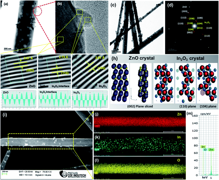 |
| | Fig. 2 (a and c) TEM images of ZnO@In2O3 heterojunction nanowires, (b) HRTEM image of ZnO@In2O3 nanowires, (d) SAED pattern of ZnO@In2O3 nanowires, (e–g) the inverse FFT images and estimation of lattice spacing of ZnO, In2O3 interface and In2O3 nanoisland planes, (h) simulated crystal planes of ZnO and In2O3, (i) FE-SEM image of ZnO@In2O3 heterojunction nanowires, (j–l) corresponding EDS Elemental maps of ZnO@In2O3 heterojunction nanowires and (m) the EDX spectrum shows the presence of Zn, In and O elements. | |
These virtual crystal planes were simulated for visualizing the exposed facets along with the dangling bonds and correlated with HRTEM analysis. For the (002) lattice plane terminated with Zn2+, the chemisorption capability could be preferred since the Zn2+ ions existing on the (002) plane are able to seize more oxygen from the atmosphere which further responds towards NO2 molecules through unsaturated oxygen coordination aided by physisorption processes.39Fig. 2(h) presents the simulated crystal plane after slicing the (002) facet of ZnO, the (104) facet of In2O3 and the (110) interface facet of the In2O3 crystal structure. From the crystallographic simulation studies, it was evident that the (002) plane possesses only Zn2+ on the exposed lattice which can facilitate the adsorption of NO2 molecules and further entrap the electrons and get reduced. Likewise, the (104) and (110) planes of In2O3 terminated with In3+ ions on the exposed polar planes are also able to grasp the oxygen from the atmosphere and further aid in physical or chemical adsorption of NO2 molecules.40 The ZnO (002) plane terminated with Zn2+ ions and surface anchored In2O3 nanoislands forms the heterojunction structure. The In3+ terminated planes with the exposed facets of (104) and (110) of In2O3 boost the adsorption kinetics of NO2 molecules at the heterojunctions. Thus, the crystallographic analysis could predict that the superior adsorption of NO2 could be mainly caused due to the existence of ZnO/In2O3 polar surfaces by strong dual interactions between Zn2+ and In3+ ions on the heterojunctions, which act as a major driving force for the surface reactions during the sensing process.41 Moreover, the FE-SEM analysis with EDX elemental mapping clearly signified the distribution of Zn, In and O elements on the surface of ZnO as depicted in Fig. 2(i–m), confirming the formation of the ZnO@In2O3 heterojunction nanowires.
TEM analysis (Fig. 2(c) and S3†) also revealed the presence of mesoporous structures of the ZnO nanowires which was further correlated and confirmed from N2 adsorption and desorption studies using BET analysis as depicted in Fig. S3.† Both porous and non-porous materials exhibited a characteristic type-IV reversible curve associated with the hysteresis loops at partial pressure ranging from 0.0 to 0.9, representing the presence of a mesoporous structure. The specific surface area, pore volume and pore size of bare ZnO, mesoporous ZnO and mesoporous ZnO@In2O3 heterojunction nanowires were estimated as tabulated in Table S1.† The high surface area illustrates the presence of excess active sites on the surface that could aid in easy charge transfer, which can be reflected in superior gas sensing characteristics of the mesoporous ZnO@In2O3 heterojunction nanowires.20
XPS analysis of ZnO@In2O3 heterojunction nanowires
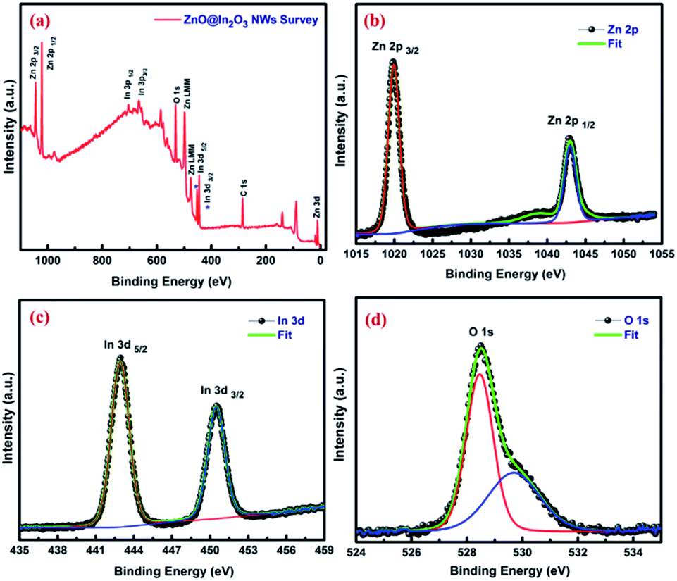
The surface characteristics of ZnO@In2O3 heterojunction nanowires were further examined by XPS analysis. The survey scan spectrum of the ZnO@In2O3 nanowires is depicted in Fig. 3(a). The peaks related to C 1s could originate from the ligands settled during the chemical synthesis and also due to carbon contamination typically found in the survey spectrum. The well-resolved peaks at binding energy values of 1019.8 and 1042.8 eV could be assigned to Zn 2p3/2 and Zn 2p1/2 respectively, as shown in Fig. 3(b) whereas, Fig. 3(c) presents the high-resolution In 3d state of ZnO@In2O3 heterojunction nanowires. For In2O3, a couple of peaks located at 442.9 and 450.5 eV is attributed to the binding energies of In 3d5/2 and In 3d3/2, respectively. Fig. 3(d) shows broad and asymmetric O 1s profiles deconvoluted into symmetrical peaks sited at 528.5 and 529.64 eV, respectively indicating a pair of oxygen species ionosorbed on the material. The peak at a binding energy of 528.5 eV is supposed to have originated from the lattice oxide, O2− in the ZnO, whereas the adjacent peak residing at the binding energy 529.64 eV is ascribed to ionosorbed O− on the surface of ZnO nanowires.42
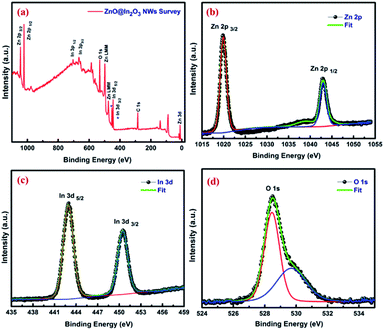 |
| | Fig. 3 (a) XPS wide range survey scan spectrum and high resolution spectra corresponding to (b) Zn 2p (c) In 3d and (d) O 1s of ZnO@In2O3 heterojunction nanowires. | |
Room-temperature local current–voltage characteristics of ZnO@In2O3 heterojunction nanowires
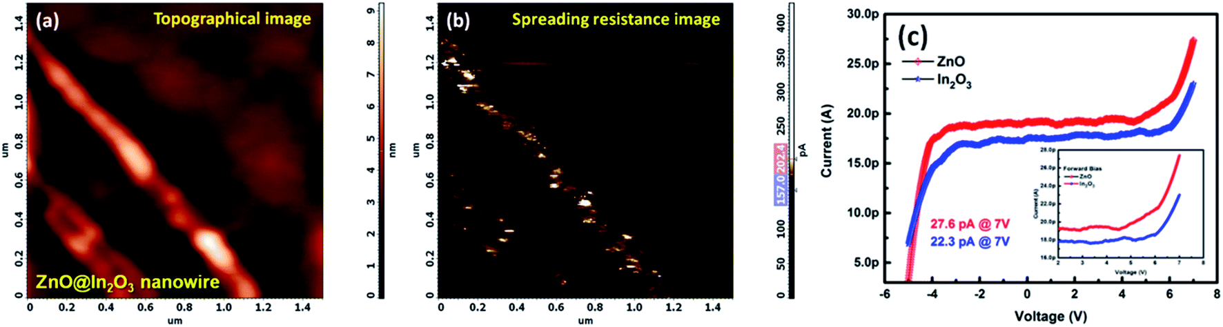
Scanning Spreading Resistance Microscopy (SSRM) imaging was employed to map the local charge transport properties of ZnO@In2O3 heterojunction nanowires at room temperature. Fig. 4(a) shows the topography image of n–n type ZnO@In2O3 heterojunction nanowires using contact mode AFM imaging. During contact mode SSRM imaging, a bias voltage of ±5 V was applied between the conductive tip and the material, as depicted in Fig. 4(b), wherein the resulting current was passed through the tip and sample and was measured in order to visualize the local spreading resistance. The local electrical conductivity map (Fig. 4(b)) of the n–n type ZnO@In2O3 heterojunction nanowires coated on a conductive silicon substrate clearly reveals local electron conduction characteristics across the ZnO@In2O3 heterojunction nanowires. The corresponding current–voltage (I–V) curves were obtained from various locations on the surface of heterojunction nanowires. The intention of this particular study was to analyze the local electron transport characteristics of the ZnO@In2O3 nanowires, in which the conduction in ZnO nanowires (27.6 pA) was found to be comparatively higher compared to that in In2O3 nanoislands (22.3 pA) as evident from Fig. 4(c). It can also be emphasized that the material demonstrated good electrical conductivity at room temperature exclusive of any additional heating to move the electrons within the energy bands. Based on the observation from the SSRM imaging and local current–voltage characteristics of ZnO@In2O3 heterojunction nanowires, it can be ascertained that charge accumulation and depletion can occur at the interface of heterojunctions (Scheme 3(b)) as clearly evident from the color contrast across the nanowires.43 This can be directly correlated with individual band structures of the semiconducting heterojunctions. While forming the heterojunction, electrons transfer from a lower work function to higher work function material. Hence, the charge transfer occur from In2O3 to ZnO by which a charge depletion region can be significantly formed at the In2O3 junctions implying the electronic upward bending caused by charge recombination at the interface.44 In contrast, ZnO (n-type semiconductor) shows higher electron accumulation near to the heterojunction interface, which leads to downward band bending. Therefore, the charge density of ZnO nanowires was found to be higher than that of In2O3 nanoislands, which can lead to remarkably superior NO2 gas sensing properties owing to the distinctive n–n heterojunction hot spots on the surface of ZnO.
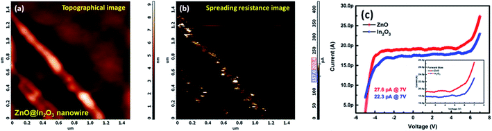 |
| | Fig. 4 (a) AFM topography and (b) corresponding SSRM images of ZnO@In2O3 heterojunction nanowires, (c) localized I–V characteristics of ZnO and In2O3 nanoparticles (inset shows the forward bias I–V curve). | |
Evaluation of the NO2 sensing performance of ZnO@In2O3 heterojunction nanowires
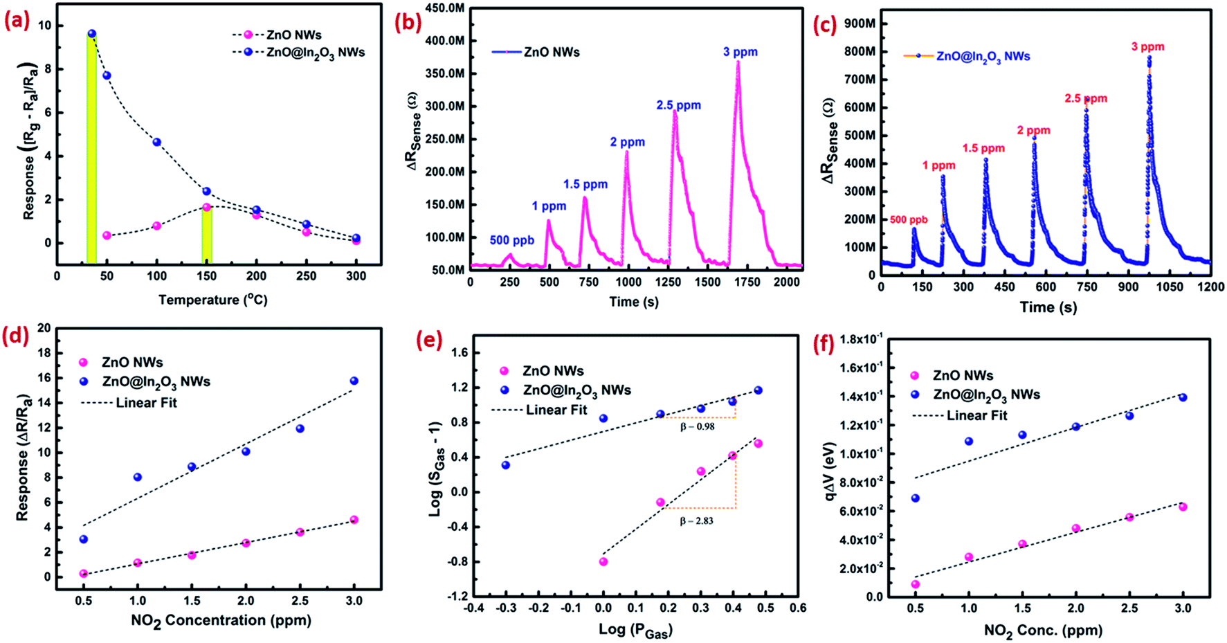
The NO2 sensing properties of mesoporous ZnO@In2O3 heterojunction nanowires were evaluated using an in-house gas sensor test station.32 In order to estimate the operating temperature, the sensor response (S), [(Rg − Ra)/Ra] upon introduction of 1 ppm of NO2 gas at different temperatures (RT – 300 °C) was assessed as shown in Fig. 5(a) for porous ZnO nanowires and porous ZnO@In2O3 heterojunction nanowires. The enhanced response toward NO2 was estimated to be at 150 °C and 34 °C for porous ZnO nanowires and porous ZnO@In2O3 heterojunction nanowires respectively, which were identified as the working temperatures of these sensing materials. The heterojunction nanowires exhibited a significantly reduced working temperature compared to pristine ZnO nanowires. The observed higher response of ZnO@In2O3 heterojunction nanowires under ambient conditions is due to the charge transfer between ZnO and In2O3 due to the difference in work functions. Phenomenally, this process leads to charge accumulation and also the depletion region formed at the interfaces of the heterojunction. Hence, the energy desired to reach the highest response will be minimal for heterojunction ZnO@In2O3 compared to pristine ZnO nanowires which is responsible for its lower operating temperature.
 |
| | Fig. 5 (a) Response towards exposure to 1 ppm of NO2 as a function of temperature, (b and c) dynamic NO2 sensing characteristics, (d) NO2 response graph, (e) log(SGas − 1) against logPg plot of curves and (f) variations in the band bending energy graph of ZnO nanowires and ZnO@In2O3 heterojunction nanowire based sensors. | |
The dynamic NO2 response characteristics of ZnO nanowires and ZnO@In2O3 heterojunction nanowires towards exposure to various concentrations of NO2 gas at their optimal operating temperature are depicted in Fig. 5(b and c). The increase in resistance was observed when the material was exposed to NO2, which is the typical n-type behavior of a semiconductor and also ascertained with the porous structure of the nanowires. As the gas concentration was increased, the change in resistance was also found to be simultaneously increased. During the sensing property evaluation, the NO2 gas was introduced along with (N2) carrier flow after attaining the stable baseline resistance without any fluctuation. The adsorption of NO2 gas continued till the saturation was achieved and desorption occurred when NO2 flow was stopped. The relative response against different concentrations of NO2 in the range of 500 ppb to 3 ppm was estimated as shown in Fig. 5(d). The NO2 sensor parameters of ZnO nanowires and ZnO@In2O3 heterojunction nanowires are summarized in Table S2.† The selectivity of the gas sensor is an important parameter for considering them for real time applications. The responses of interfering gases, such as H2S, NH3, SO2, acetone and ethanol were tested at a constant concentration of 2 ppm under ambient conditions. The ZnO@In2O3 heterojunction nanowires exhibited good selectivity towards NO2 gas at room temperature as evident from Fig. S6† compared to other gases. Hence, NO2 was chosen as the analyte gas for further studies.
Upon exposure of the heterojunction nanowires towards the NO2 environment, the NO2 molecules initially react with negatively charged O2−, and O− ions and seize more electrons from the conduction band rather than interacting directly with the surface. This process reduces the electron accumulation region width (LD) and increases the resistance. Therefore, in order to explore the NO2 detection mechanism of n–n type ZnO@In2O3 heterojunction nanowires, the state of ionosorbed oxygen molecules has to be initially examined. The sensor response of the material and quantity of the analyte could be correlated with,45
| |  | (4) |
| | | log(Sg−1) = βlog(Pg) + logα | (5) |
where,
α is the prefactor and
β is the typical exponent for partial pressure dependence and
Pg is the analyte concentration. The
β value decides the nature of surface oxide species and also elementary reactions that occur on the material surface. If
β is equal to 0.5, the surface oxide ions could be O
2− also if
β is ∼1, the surface oxide ions could be O
−. This could be deduced using the relation log(
Sg − 1) against log(
Pg) as shown in
Fig. 5(e). As estimated from the slope of the straight line in
Fig. 5(e), the
β value was calculated to be 2.89 for ZnO nanowires and 1.33 for ZnO@In
2O
3 heterojunction nanowires at room temperature, signifying that the primary surface oxide species present on ZnO@In
2O
3 nanowires are O
2− rather than O
− ions.
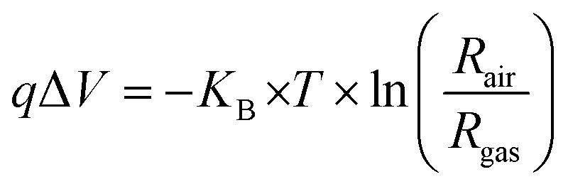
Moreover, band bending at the heterojunction surface was further estimated based on the sensor response values of ZnO nanowires and ZnO@In2O3 heterojunction nanowires. According to the Boltzmann distribution law, the density of free electrons (ns) and band energy (qΔV) corresponding to the materials can be related as given below;46,47
| |  | (6) |
where,
KB is the Boltzmann constant and
T is the operating temperature.
Rgas is the resistance in a NO
2 atmosphere and
Rair is the resistance in the ambient atmosphere. The band bending can be determined from the sensor response values corresponding to different concentrations of analyte NO
2. The quantification of
qΔ
V affirmed that ZnO@In
2O
3 heterojunction nanowires possessed high
qΔ
V energy values compared to pristine ZnO nanowires due to the broader depletion region in the presence of NO
2 as deduced from
Fig. 5(f). From this analysis it can be inferred that the existence of ZnO/In
2O
3 heterojunction interfaces could be responsible for the preferential electron transport and superior NO
2 adsorption process.
To understand the NO2 adsorption kinetics, the Elovich equation was used and variation of (Ctg − C0) versus ln(t) was plotted with the help of the response/recovery profiles corresponding to exposure to different concentrations of NO2 as depicted in Fig. S5(a and b).† As per eqn (S1),† the plot between (Ctg − C0) versus ln(t) is supposed to be linear.48,49 Fig. S5(a and b)† illustrate the adsorption isotherms of ZnO nanowires and ZnO@In2O3 heterojunction nanowires, which showed an almost linear trend upon exposure to NO2 gas. The rate of adsorption can be estimated for different ppm levels of NO2 which followed a linear trend upon increasing concentration of NO2 (Fig. S5(c)).† The initial adsorption rate was calculated to be 0.93 Ω−1 s−1 at 150 °C for ZnO nanowires and 10.76 Ω−1 s−1 at room temperature for ZnO@In2O3 heterojunction nanowires towards 1 ppm of NO2 exposure. Further, reduction in the adsorption rate was noticed upon an increase in the NO2 concentration owing to continuous cycling of NO2. The effect of concentration on NO2 adsorption kinetics was analyzed, which showed an increase in the potential barrier with respect to the NO2 concentration. At elevated concentrations, accessibility of NO2 molecules was higher on the surface of heterojunction nanowires and therefore, the potential barrier increased as depicted in the Fig. S5(d).† The interference of humidity in the NO2 sensing performance of ZnO@In2O3 heterojunction nanowires was studied as shown in Fig. S7(a and b).† The response was found to be relatively constant in the RH (relative humidity) range of 10% to 55%. However, the sensitivity reduced rapidly when the humidity exceeded 60% due to higher RH% interference as moisture adhered on the sensing material restricting the electron transfer between the gas/material interface. The results reveal that ZnO@In2O3 heterojunction nanowires have excellent stability at a lower humidity range at room temperature.
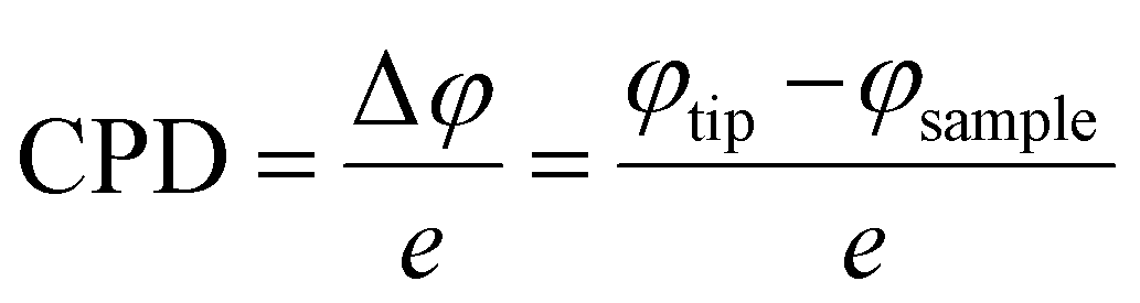
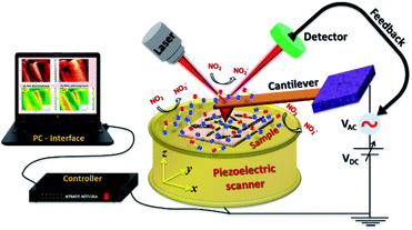
Exploration of a plausible NO2 sensing mechanism by in situ SKPM analysis
Scanning Kelvin probe microscopy was further implemented to explore the surface potential (SP) variations of the ZnO nanowires and n–n type ZnO@In2O3 heterojunction nanowires during exposure to the NO2 gas environment. By moving the conducting probe towards the material, a biased potential difference is generated owing to the variation in the Fermi energies between the probe and the material.50 The local charge transport mechanism during NO2 gas sensing was further probed by monitoring the surface potential or contact potential difference (CPD) mapping of the n–n type heterojunction nanowires using SKPM during exposure to the NO2 gas environment as shown in Scheme 2. The work function, (φ) of a MOS is defined as the quantity of energy needed to move an electron present in the surface of the semiconductor material to the vacuum level.51 A high surface charge density on the material surface therefore promotes higher φ, allowing the visualization of charge accumulation/depletion on the surface of the material. During SKPM analysis, a tungsten carbide coated silicon nitride probe was allowed to interact electronically with the material surface. The contact potential difference (CPD) was measured from the difference between the Fermi levels of the conducting probe and the material surface.52 The work function of the material (φ) was determined from the CPD value with the work function of the SKPM cantilever tip, φ(tip). Before proceeding with SKPM measurements on the heterojunction nanowires, the tungsten carbide coated silicon nitride probe was calibrated on a pure Au thin film under similar conditions (Fig. S4†). The contact potential difference of the Au film was measured to be ∼32 mV. The work function of the conducting probe (φtip) was initially calibrated as 4.9 eV estimated using the known work function (φ(Au) = 5.1 eV) of the Au sputtered thin film in order to change the calculated CPD into the work function of the material. Moreover, the contact potential difference is extremely material-dependent and directly associated with the work function of the material and surface dipole moments. In the case of semi-conductors, there can be contributions from charge distribution on the material and surface dipoles and from electronic rearrangements at the material/substrate interface. The difference in the work function of the SKPM probe and the material was calculated using the following equations;| | 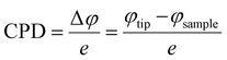 | (7) |
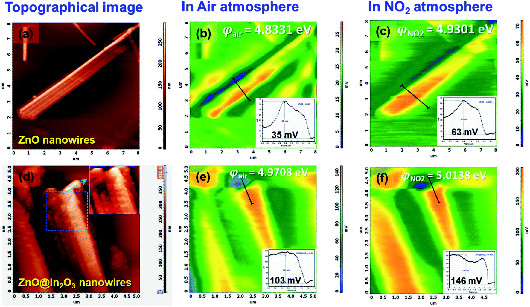
where e is the charge, φtip is the work function of the conducting probe and φsample is the work function of the semiconductor material.53 The topographic AFM images and the corresponding SKPM images of ZnO nanowires and ZnO@In2O3 heterojunction nanowires before and during NO2 exposure are shown in Fig. 6. The CPD before NO2 exposure was found to be ∼35 mV and a two fold increase in CPD upto ∼63 mV was calculated when NO2 was introduced on ZnO nanowires. The work function (φ) of ZnO nanowires was estimated to be 4.83 eV before NO2 exposure and the work function increased upto 4.93 eV in the NO2 environment. Upon exposure to NO2 gas, electron transfer occurs between adsorbed NO2 and the surface of nanowires which is mainly due to the active oxygen defects and ionosorbed oxide species. The electron depletion leads to increase in CPD which is evident from the SKPM images depicted in Fig. 6(a–c). The morphology and surface potential distribution mapping using SKPM on ZnO@In2O3 heterojunction nanowires before and after exposure to the NO2 environment are depicted in Fig. 6(d–f). The CPD value of ZnO@In2O3 heterojunction nanowires was found to be increased to 103 mV compared to pristine ZnO nanowires (35 mV) in the absence of the NO2 environment. This enhancement in the CPD value is due to the charge transport between the heterojunction materials (In2O3 and ZnO). The electrons in both ZnO nanowires and In2O3 nanoislands acquire different work functions and binding energies when they are electrically connected. Typically, the electrons can move from the material with higher Fermi energy to the material with lower Fermi energy since the work function absolutely depends on the Fermi level. Hence, there could be accumulation of charge and also formation of a depletion region at the heterojunction interfaces. The work function of ZnO@In2O3 heterojunction nanowires was calculated to be 4.97 eV, which is higher than that of bare ZnO nanowires (φair = 4.83 eV). The increase in the work function indirectly indicates the difference in the Fermi level and surface band bending. The CPD further increased up to 146 mV upon exposure to the NO2 environment and the corresponding work function was calculated to be 5.02 eV. This enhancement in the CPD value is proportional to the variation in the work function of heterojunction interfaces which can be visualized in the SKPM images as depicted in Fig. 6(d–f). The inset shows the SKPM line scan, denoted by a dark line in Fig. 6(a–c) and (e–f), to measure the CPD before and during NO2 exposure.
 |
| | Scheme 2 Schematic representation of in situ SKPM imaging performed for ZnO@In2O3 heterojunction nanowires in the NO2 gas environment. | |
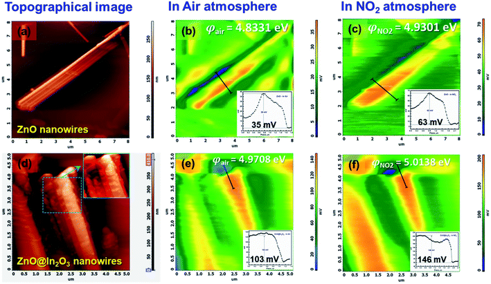 |
| | Fig. 6 Representative AFM topographical images of (a) ZnO nanowires and (d) ZnO@In2O3 heterojunction nanowires (inset shows the magnified image of heterojunction nanowires), (b and c) SKPM images of ZnO nanowires in air and the NO2 environment and (e and f) SKPM images of ZnO@In2O3 heterojunction nanowires in air and NO2 environments (inset shows the CPD in air and the NO2 environment). | |
The contact potential difference (eVCPD) between the conducting scanning probe and the material surface corresponds to the variation in their work functions (φtip – φs).54 The work function of the semiconductor materials can be estimated using the relations;
| | | φs = −χs + ΦB + (EC − EF) | (9) |
| | | eVCPD = φtip − χs + ΦB + (EC − EF) | (10) |
where,
e is the elementary charge,
χs is the electron affinity of the sample,
ΦB is the surface band bending, (
EC −
EF) is the difference in the Fermi energy (
EF) also conduction band (
EC) of the material. It is known that the surface potential of the semiconductor materials relies on the surface band bending (
ΦB), the electron affinity (
χs) and the carrier concentration. The surface band bending (
Φ) was calculated for ZnO nanowires and ZnO@In
2O
3 heterojunction nanowires before and after NO
2 gas exposure using the following equation,
| | | ΦB = φM − qVCPD + φoff − χ + (EC − EF) | (11) |
where,
χ is the electron affinity of the ZnO (3.2 eV),
φoff is the offset in the estimated work function of the conducting probe found during calibration (∼32 meV) on the Au film (
φM = 5.1 eV) and
EF is the Fermi level related to the conduction band minimum.
28 Using
eqn (11), the estimated surface band bending (SBB) of ZnO nanowires before NO
2 exposure was 1.92 eV which was increased upto 1.96 eV during NO
2 exposure. Interestingly, the surface band bending for ZnO@In
2O
3 heterojunction nanowires was increased up to 2.04 eV compared to pristine ZnO nanowires. During NO
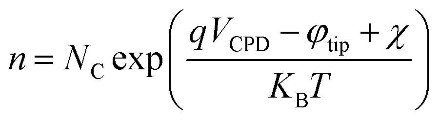
2 exposure, the SBB value increased further up to 2.1 eV which implied the formation of a vast depletion region in the heterojunction nanowires. Based on Boltzmann approximation, the electron density of the ZnO nanowires and ZnO@In
2O
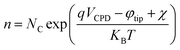
3 heterojunction nanowires could be estimated, in which the concentration of electrons in n-type semiconductors can be expressed as,
| | 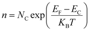 | (12) |
| |  | (13) |
where,
EC and
EF are the conduction band and the Fermi energy level,
Nc is the effective density of states,
T is the temperature and
KB is the Boltzmann constant.
54 Here, the work function of Au was ascertained to be 5.1 eV,
Nc of ZnO is 3.7 × 10
18, electron affinity of ZnO (
χ) is 4.5 eV, the Boltzmann constant,
KB is 8.6 × 10
15 eV K
−1 and temperature,
T is 300 K. The carrier density of ZnO nanowires and ZnO@In
2O
3 heterojunction nanowires before and during NO
2 exposure was calculated from SKPM analysis using
eqn (13). The carrier density of ZnO@In
2O
3 heterojunction nanowires decreased drastically from 1.18 × 10
19 cm
−2 to 0.87 × 10
19 cm
−2 during NO
2 exposure. The reduction in charge density clearly states that the charge recombination occurs when the NO
2 molecules are adsorbed on ZnO@In
2O
3 heterojunction nanowires and entrap the electrons present in the conduction band. The space charge region formed due to the SBB at the heterojunction can be described by the depletion width (
W) and can be expressed as,
28| | 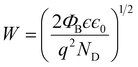 | (14) |
The depletion width (W) formed due to surface band bending and charge carrier density was further calculated from SKPM analysis of ZnO nanowires and ZnO@In2O3 heterojunction nanowires using eqn (14) which is summarized in Table S4.† The depletion width (W) was found to be increased up to 3.19 nm for heterojunction nanowires compared to pristine ZnO nanowires. During NO2 exposure, the estimated depletion width was estimated for ZnO nanowires and ZnO@In2O3 heterojunction nanowires to be 3.34 nm and 3.81 nm respectively. The estimated changes in the work function (φs), depletion width (W), surface band bending (ΦB) and carrier density (ns) values resulting from in situ SKPM analysis were further used to deduce the NO2 sensing mechanism of the ZnO@In2O3 heterojunction nanowires. Based on the above experimental evidence, it can be concluded that the variations in the surface potential of the heterojunction nanowires was increased with decreasing electron density upon NO2 exposure. The electron–hole pair recombination increases due to the increase in carrier density which favors the charge transport between In2O3 to ZnO at the heterojunctions.
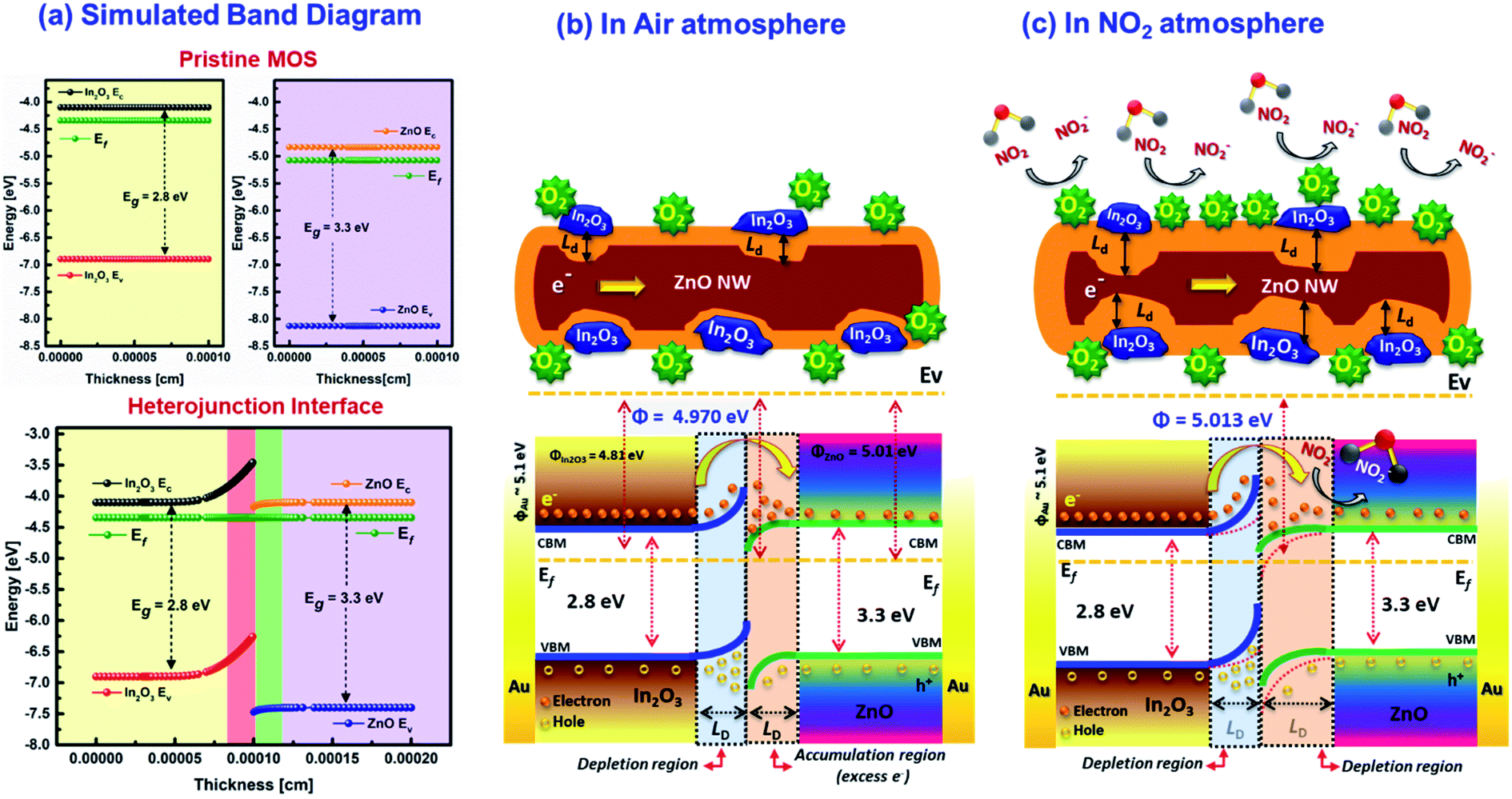
Based on the evidences from SKPM analysis, the electronic band structure was further theoretically constructed using AFORS-HET v2.5 as shown in Scheme 3(a). The simulated energy band diagram clearly revealed the upward bending state at In2O3 and the downward bending state at ZnO interfaces owing to the electron transfer at the heterojunctions due to the difference in their Fermi level energies. The carrier density reaches equilibrium when the Fermi level of the ZnO and In2O3 becomes aligned, while forming heterojunctions. The trapping of electrons at the surface states drastically reduced the surface potential properties. While considering the core-ZnO nanowires, the surface could be occupied by more free electrons than pristine ZnO due to the formation of heterojunctions with In2O3. This induces a downward bending state and electrons tend to accumulate near the surface of the semiconductor. When electron rich heterojunction nanowires were exposed to NO2 gas, a majority of carriers tend to be trapped by NO2 through adsorbed surface oxygen ions (O2−) and the potential barrier of 1D nanowires increased as the carrier density decreases resulting in increase in both the SBB and depletion width.
 |
| | Scheme 3 (a) Simulated energy band diagram before and after contact and schematic diagram showing the NO2 sensing mechanism (b) in air atmosphere and (c) in the NO2 gas atmosphere, deduced for ZnO@In2O3 heterojunction nanowires. | |
Usually when metal oxide materials are exposed to an oxygen atmosphere, various oxide ions molecules like O2−, O− and O2− are adsorbed on the material surface as a function of temperature leading to electron depleted regions on the surface of semiconductor materials.55 At lower working temperatures, more O2− ions can be adsorbed over the surface of ZnO nanowires. The response of the sensor and rate of adsorption of NO2 molecules may also depend on the surface adsorbed O2− ions. Based on the β value obtained from the NO2 gas sensing profile, the dominant oxygen species adsorbed over the surface of ZnO@In2O3 nanowires were found to be O2− rather than O− ions. When the ZnO@In2O3 nanowires are exposed to NO2 gas molecules, the molecules electrically react with negatively adsorbed oxygen molecules and further entrap more electrons at the interfaces of the heterojunction as represented by the given equation:
| | | NO2(gas) + e− → NO2(ads)− | (15) |
| | | NO2(gas) + O2(ads)− + 2e− → NO2(ads)− + 2O(ads)− | (16) |
Based on the experimental evidence and theoretical prediction, the energy diagram of n-ZnO/n-In2O3 heterojunction nanowires is proposed as illustrated in Scheme 3(b and c). The n–n heterojunctions created between n-type ZnO nanowires and n-type In2O3 nanoislands could play a crucial role in tuning the gas sensing performance of the ZnO@In2O3 nanowire based sensor. When In2O3 and ZnO are hybridized to form the n–n type heterojunction, an interfacial electric field could be formed at the interface between ZnO and In2O3. The energy band-gaps of ZnO and In2O3 were calculated from UV-DRS experiments as 3.31 and 2.75 eV, respectively. Based on these estimated parameters, the simulated band structure designed for n-ZnO and n-In2O3 is shown in Scheme 3(a). The energy band bending state through charge transport, the positions of the conduction and valance bands of n-ZnO/n-In2O3 heterojunctions were clearly understood by simulating the energy band structure using the evidence obtained from the SKPM analysis.
Prior to electrical contact, the Fermi energy of ZnO is lower than that of In2O3 owing to its lower work function illustrated in Scheme S1.† Once these two dissimilar metal oxides with varied work functions are brought into electrical contact, the electrons move out of from higher Fermi energy (In2O3) to lower Fermi energy (ZnO) until the energy levels achieve equilibrium.56,57 In the meantime, an interfacial electric charge aligning from core-ZnO to In2O3 is formed at the interfaces. Under air atmosphere (Scheme 3(b)), both In2O3 nanoislands and ZnO nanowires adsorb negatively charged oxygen ions owing to the oxygen adsorption over the sensor material. As a result of the built-in interfacial electric field, the electrons in the conduction band of In2O3 can move to the excited ZnO, and at the same time, holes reside in the valence band of n-In2O3. Hence, adsorbed oxygen draw electrons from the semiconductor material, making the n-type In2O3 more depleted. This lowered the e− concentration leads to an upward bending state. Likewise, n-type ZnO become more conductive i.e., an increased e− concentration causing a downward bending state. Similarly, when the n–n heterointerface is in contact, the electrons build up near the ZnO/In2O3 junctions forming a depletion region across the In2O3 junctions.58 During NO2 exposure which is a strong oxidizing gas, the NO2 molecules trap e− by interaction with O2− ions adsorbed on ZnO and In2O3 interfaces by means of electron transport between the heterojunction interfaces of ZnO@In2O3 nanowires and NO2 gas molecules as demonstrated in Scheme 3(c). While NO2 is a potential oxidizing gas with an excessive electron affinity of 2.28 eV in contrast to 0.43 eV of oxygen. The NO2 gas reacts with the semiconductor heterojunction material via ionosorbed O2− species and the potential barrier increases at heterojunction as manifested from in situ SSRI and SKPM studies. Furthermore, it was elucidated from the band diagram (Scheme 3(c)) of n–n ZnO@In2O3 heterojunction nanowires that a denser depletion region is formed over the surface of ZnO owing to the electron–hole recombination at the heterojunctions than over In2O3 upon NO2 exposure as revealed from the experimental evidence stated in the in situ SKPM analysis (Fig. 6(f)). Moreover, the crystallographic defects and enhanced surface area owing to the mesoporous structure of the ZnO@In2O3 nanowires provided favourable adsorption facets for a fast response to gaseous NO2, which could amplify the gas sensing properties. The gas sensing characteristics of the mesoporous ZnO@In2O3 heterojunction nanowire sensor under ambient conditions are therefore considered to be improved by its distinctive morphological and electrical properties.
Conclusions
To conclude, 1-D mesoporous n–n type ZnO@In2O3 heterojunction nanowires were effectively synthesized via a simple two step hydrothermal method and their local electrical characteristics and NO2 sensing properties at a reduced operating temperature were thoroughly investigated. Surface-modified In2O3 nanoislands on the ZnO nanowires were characterized by various characterization techniques. XRD and HRTEM analyses illustrated the structure of ZnO@In2O3 heterojunction nanowires as In2O3 nanoislands decorated uniformly over the surface of mesoporous ZnO nanowires. The simulated lattice structure supported by HRTEM analysis was used to presume the NO2 adsorption on the heterojunction nanowires. The crystallographic analysis was adopted to ascertain the dangling bonds and also estimate the proportion of metals ions to oxygen ions existing at the exposed heterojunction crystal facets. The localized charge transfer process was visualized using spreading resistance imaging, where the maximum electrical conduction occurred at the ZnO sites rather than In2O3 due to the electron transfer between the heterojunctions. The enhanced NO2 sensing performance of the ZnO@In2O3 sensor is ascribed to the formation of effective n-In2O3/n-ZnO heterojunctions, resulting in a rapid response time (4–6 s) and 10 times superior sensitivity to ZnO nanowires with a detection limit of 500 ppb of NO2. Room temperature in situ SKPM analysis under NO2 exposure showed increment in the work function, band bending and depletion width while forming heterojunctions and revealed the local charge transfer processes in heterojunction nanowires pertaining to the NO2 sensing process. The boosting of the performance of the sensor was essentially due to Schottky n–n heterojunctions formed at the interfaces of ZnO–In2O3 and also due to the increased carrier concentration and rate of oxygen adsorption. This induced the electron depletion layer leading to enhanced NO2 gas sensitivity and good selectivity at room temperature. New insights into the sensing mechanism pertaining to n–n type ZnO@In2O3 based heterojunction nanowires revealed during this study can be useful for designing novel n–n type MOS heterojunction materials for the development of high performance NO2 sensors at a reduced operating temperature for real-time applications.
Conflicts of interest
There are no conflicts to declare.
Acknowledgements
The authors would like to acknowledge DST-SERB (SB/S3/CE/038/2015) for financial support. The authors also wish to acknowledge the facilities and support provided by the management, PSG Sons and Charities, Coimbatore.
Notes and references
- S. Bai, J. Guo, J. Sun, P. Tang, A. Chen, R. Luo and D. Li, Ind. Eng. Chem. Res., 2016, 55, 5788–5794 CrossRef CAS.
- L. Huang, Z. Wang, J. Zhang, J. Pu, Y. Lin, S. Xu, L. Shen, Q. Chen and W. Shi, ACS Appl. Mater. Interfaces, 2014, 6, 7426–7433 CrossRef CAS.
- J. H. Kim, A. Mirzaei, H. W. Kim and S. S. Kim, ACS Appl. Mater. Interfaces, 2019, 11, 24172–24183 CrossRef CAS.
- X. Chen, S. Wang, C. Su, Y. Han, C. Zou, M. Zeng, N. Hu, Y. Su, Z. Zhou and Z. Yang, Sens. Actuators, B, 2020, 305, 127393 CrossRef.
- Y. Zhong, W. Li, X. Zhao, X. Jiang, S. Lin, Z. Zhen, W. Chen, D. Xie and H. Zhu, ACS Appl. Mater. Interfaces, 2019, 11, 13441–13449 CrossRef CAS.
- Y. Zhang, X. Cheng, X. Zhang, Z. Major, Y. Xu, S. Gao, H. Zhao and L. Huo, Appl. Surf. Sci., 2020, 505, 144533 CrossRef.
- J. Zhang, D. Zeng, Q. Zhu, J. Wu, Q. Huang and C. Xie, J. Phys. Chem. C, 2016, 120, 3936–3945 CrossRef CAS.
- Z. Wang, G. Men, R. Zhang, F. Gu and D. Han, Sens. Actuators, B, 2018, 263, 218–228 CrossRef CAS.
- F. Eisner, A. Seitkhan, Y. Han, D. Khim, E. Yengel, A. R. Kirmani, J. Xu, F. P. García de Arquer, E. H. Sargent, A. Amassian, Z. Fei, M. Heeney and T. D. Anthopoulos, Sol. RRL, 2018, 2, 1800076 CrossRef.
- B. H. Kim, C. M. Staller, S. H. Cho, S. Heo, C. E. Garrison, J. Kim and D. J. Milliron, ACS Nano, 2018, 12, 3200–3208 CrossRef CAS.
- D. Zhang, J. Wu, P. Li, Y. Cao and Z. Yang, ACS Appl. Mater. Interfaces, 2019, 11, 31245–31256 CrossRef CAS.
- D. Zhang, Z. Yang, Z. Wu and G. Dong, Sens. Actuators, B, 2019, 283, 42–51 CrossRef CAS.
- D. Zhang, Z. Yang, P. Li and X. Zhou, Sens. Actuators, B, 2019, 301, 127081 CrossRef CAS.
- W. Yang, P. Wan, X. Zhou, J. Hu, Y. Guan and L. Feng, ACS Appl. Mater. Interfaces, 2014, 6, 21093–21100 CrossRef CAS.
- S. Bai, H. Fu, Y. Zhao, K. Tian, R. Luo, D. Li and A. Chen, Sens. Actuators, B, 2018, 266, 692–702 CrossRef CAS.
- J. Sun, L. Sun, N. Han, J. Pan, W. Liu, S. Bai, Y. Feng, R. Luo, D. Li and A. Chen, Sens. Actuators, B, 2019, 285, 68–75 CrossRef CAS.
- Y. S. Haiduk, A. A. Khort, N. M. Lapchuk and A. A. Savitsky, J. SolidState Chem., 2019, 273, 25–31 CrossRef CAS.
- N. Ramgir, R. Bhusari, N. S. Rawat, S. J. Patil, A. K. Debnath, S. C. Gadkari and K. P. Muthe, Mater. Sci. Semicond. Process., 2020, 106, 104770 CrossRef CAS.
- S. Roso, D. Degler, E. Llobet, N. Barsan and A. Urakawa, ACS Sens., 2017, 2, 1272–1277 CrossRef CAS.
- K. Zhang, S. Qin, P. Tang, Y. Feng and D. Li, J. Hazard. Mater., 2020, 391, 122191 CrossRef CAS.
- L. Ma, H. Fan, H. Tian, J. Fang and X. Qian, Sens. Actuators, B, 2016, 222, 508–516 CrossRef CAS.
- K. Xu, S. Tian, J. Zhu, Y. Yang, J. Shi, T. Yu and C. Yuan, Nanoscale, 2018, 10, 20761–20771 RSC.
- K. Li, Y. Luo, B. Liu, L. Gao and G. Duan, J. Mater. Chem. A, 2019, 7, 5539–5551 RSC.
- P. Hozák, M. Vorokhta, I. Khalakhan, K. Jarkovská, J. Cibulková, P. Fitl, J. Vlček, J. Fara, D. Tomeček, M. Novotný, M. Vorokhta, J. Lančok, I. Matolínová and M. Vrňata, J. Phys. Chem. C, 2019, 123, 29739–29749 CrossRef.
- X. Xiao, L. Liu, J. Ma, Y. Ren, X. Cheng, Y. Zhu, D. Zhao, A. A. Elzatahry, A. Alghamdi and Y. Deng, ACS Appl. Mater. Interfaces, 2018, 10, 1871–1880 CrossRef CAS.
- D. Degler, N. Barz, U. Dettinger, H. Peisert, T. Chassé, U. Weimar and N. Barsan, Sens. Actuators, B, 2016, 224, 256–259 CrossRef CAS.
- C. Drouilly, J. M. Krafft, F. Averseng, S. Casale, D. Bazer-Bachi, C. Chizallet, V. Lecocq, H. Vezin, H. Lauron-Pernot and G. Costentin, J. Phys. Chem. C, 2012, 116, 21297–21307 CrossRef CAS.
- A. Patsha, P. Sahoo, S. Amirthapandian, A. K. Prasad, A. Das, A. K. Tyagi, M. A. Cotta and S. Dhara, J. Phys. Chem. C, 2015, 119, 21251–21260 CrossRef CAS.
- A. Kaur and R. Kumar, Sens. Actuators, A, 2016, 245, 113–118 CrossRef CAS.
- Y. Feng, K. Zhang, H. Li, F. Wang, B. Zhou, M. Fang, W. Wang, J. Wei and H. S. P. Wong, Nanotechnology, 2017, 28, 295705 CrossRef.
- C. E. Kehayias, S. MacNaughton, S. Sonkusale and C. Staii, Nanotechnology, 2013, 24, 245502 CrossRef.
- V. Ramakrishnan, K. G. Nair, J. Dhakshinamoorthy, K. R. Ravi and B. Pullithadathil, Phys. Chem. Chem. Phys., 2020, 22, 7524–7536 RSC.
- V. P. Dinesh, A. Sukhananazerin and P. Biji, J. Alloys Compd., 2017, 712, 811–821 CrossRef CAS.
- H. Hu, X. Huang, C. Deng, X. Chen and Y. Qian, Mater. Chem. Phys., 2007, 106, 58–62 CrossRef CAS.
- Y. Wang, S. Li, X. Xing, F. Huang, Y. Shen, A. Xie, X. Wang and J. Zhang, Chem.–Eur. J., 2011, 17, 4802–4808 CrossRef CAS.
- F. Liu, G. Huang, X. Wang, X. Xie, G. Xu, G. Lu, X. He, J. Tian and H. Cui, Sens. Actuators, B, 2018, 277, 144–151 CrossRef CAS.
- R. Zhang, P. G. Yin, N. Wang and L. Guo, Solid State Sci., 2009, 11, 865–869 CrossRef CAS.
- S. Sahoo, A. P. S. Gaur, A. K. Arora and R. S. Katiyar, Chem. Phys. Lett., 2011, 510, 242–245 CrossRef CAS.
- Y. V. Kaneti, Z. Zhang, J. Yue, Q. M. D. Zakaria, C. Chen, X. Jiang and A. Yu, Phys. Chem. Chem. Phys., 2014, 16, 11471–11480 RSC.
- S. Bai, L. Quan, P. Tang, Y. Zhao, R. Luo, A. Chen, D. Li and N. Han, IEEE Sens. J., 2016, 16, 866–872 CAS.
- Z. Xue, Z. Cheng, J. Xu, Q. Xiang, X. Wang and J. Xu, ACS Appl. Mater. Interfaces, 2017, 9, 41559–41567 CrossRef CAS.
- H. Liu, H. Zhai, C. Hu, J. Yang and Z. Liu, Nanoscale Res. Lett., 2017, 12, 2–11 CrossRef.
- M. Kitta and C. Fukada, Langmuir, 2019, 35, 8726–8731 CrossRef CAS.
- J. Y. Ma, J. Ding, H. J. Yan, D. Wang and J. S. Hu, ACS Appl. Mater. Interfaces, 2019, 11, 21627–21633 CrossRef CAS.
- J. Dhakshinamoorthy and B. Pullithadathil, J. Phys. Chem. C, 2016, 120, 4087–4096 CrossRef CAS.
- M. E. Mazhar, G. Faglia, E. Comini, D. Zappa, C. Baratto and G. Sberveglieri, Sens. Actuators, B, 2016, 222, 1257–1263 CrossRef CAS.
- M. Hübner, C. E. Simion, A. Tomescu-Stănoiu, S. Pokhrel, N. Bârsan and U. Weimar, Sens. Actuators, B, 2011, 153, 347–353 CrossRef.
- A. V. Raghu, K. K. Karuppanan and B. Pullithadathil, ACS Sens., 2018, 3, 1811–1821 CrossRef CAS.
- A. Das, V. Bonu, A. K. Prasad, D. Panda, S. Dhara and A. K. Tyagi, J. Mater. Chem. C, 2014, 2, 164–171 RSC.
- S. R. McKibbin, J. Colvin, A. Troian, J. V. Knutsson, J. L. Webb, G. Otnes, K. Dirscherl, H. Sezen, M. Amati, L. Gregoratti, M. T. Borgström, A. Mikkelsen and R. Timm, Nano Lett., 2020, 20(2), 887–895 CrossRef CAS.
- K. Tang, L. Huang, J. Lim, T. Zaveri, J. D. Azoulay and S. Guo, ACS Appl. Polym. Mater., 2019, 11(1), 2943–2950 CrossRef.
- R. Pearce, J. Eriksson, T. Iakimov, L. Hultman, A. Lloyd Spetz and R. Yakimova, ACS Nano, 2013, 7, 4647–4656 CrossRef CAS.
- M. Ali Deeb, J. Ledig, J. Wei, X. Wang, H. H. Wehmann and A. Waag, J. Appl. Phys., 2017, 122, 085307 CrossRef.
- Z. Wang, Y. Gu, J. Qi, S. Lu, P. Li, P. Lin and Y. Zhang, RSC Adv., 2015, 5, 42075–42080 RSC.
- E. Lee, Y. S. Yoon and D. J. Kim, ACS Sens., 2018, 3, 2045–2060 CrossRef CAS.
- D. Zhang, Y. Cao, J. Wu and X. Zhang, Appl. Surf. Sci., 2020, 503, 144063 CrossRef CAS.
- Z. Yang, D. Zhang and H. Chen, Sens. Actuators, B, 2019, 300, 127037 CrossRef CAS.
- G. J. Sun, J. K. Lee, S. Choi, W. I. Lee, H. W. Kim and C. Lee, ACS Appl. Mater. Interfaces, 2017, 9, 9975–9985 CrossRef CAS.
Footnote |
| † Electronic supplementary information (ESI) available. See DOI: 10.1039/d0na00318b |
|
| This journal is © The Royal Society of Chemistry 2020 |
Click here to see how this site uses Cookies. View our privacy policy here. 
 Open Access Article
 This Open Access Article is licensed under a Creative Commons Attribution-Non Commercial 3.0 Unported Licence
 *
*