
 Open Access Article
 This Open Access Article is licensed under a Creative Commons Attribution-Non Commercial 3.0 Unported Licence
B5N5 monolayer: a room-temperature light element antiferromagnetic insulator†
Dong
Zhang
 *ab,
Qihua
Xiong
cd and
Kai
Chang
*ab
*ab,
Qihua
Xiong
cd and
Kai
Chang
*ab
aSKLSM, Institute of Semiconductors, Chinese Academy of Sciences, P.O. Box 912, Beijing 100083, China. E-mail: zhangdong@semi.ac.cn; kchang@semi.ac.cn
bCenter for Excellent in Topological Quantum Computation, University of Chinese Academy of Sciences, Beijing 100190, China
cDivision of Physics and Applied Physics, School of Physical and Mathematical Sciences, Nanyang Technological University, Singapore, Singapore
dState Key Laboratory of Low-Dimensional Quantum Physics, Department of Physics, Tsinghua University, Beijing 100084, China
First published on 21st May 2020
Abstract
We demonstrate theoretically that an intrinsic antiferromagnetic phase exists in monolayer materials consisting of non-magnetic light atoms, and propose that B5N5 with a decorated bounce lattice is a thermodynamically stable two-dimensional antiferromagnetic insulator by performing state-of-the-art density functional theory calculations. The antiferromagnetic phase originates from spontaneous symmetry breaking at the nearly flat bands in the vicinity of the Fermi energy. The flat bands are formed by purely s–pz orbitals and are spin degenerate. A perpendicular electric field can remove the spin degeneracy and a prototype controllable dual spin filter with 100% spin polarization is proposed. Our proposal offers a possible two-dimensional atomically thick antiferromagnetic insulator.
1 Introduction
Magnetism, the ordered arrangement of neighbouring spins over macroscopic length scales, tends to be destroyed by thermal fluctuations above certain critical temperature, and the Curie temperatures depend critically on the dimensionality of the systems. In one dimensional (1D) systems, the long-range magnetic order only exists at T = 0,1 while in three dimensional (3D) systems, the magnetic phase transition occurs at a finite temperature. In two dimensional (2D) systems, the situation becomes more complicated. In continuous and isotropic 2D systems, according to the Mermin–Wagner theorem,2 a macroscopic magnetic order can be destroyed by long-range fluctuations at a finite temperature, because the gapless spin waves have a finite density of states and can be easily excited at any non-zero temperature. However, the exact Onsager solution to the 2D Ising model3 indicates that a magnetic phase transition occurs at a critical temperature Tc > 0. The controversial theoretical predictions make the search for 2D magnets extremely attractive in terms of both basic physics and potential applications.The family of atomically thick magnetic 2D materials has expanded rapidly in recent years, and pioneering efforts have been taken through exfoliation of monolayer and few-layer magnetic layered bulk materials, such as NiPS3,4 FePS3,5–7 and CrSiTe3.8 However, macroscopic magnetic orders are only observed in thin films. The atomically-thick CrI3 (ref. 9) and Cr2Ge2Te6 (ref. 10) down to the monolayer and bilayer limit have been successfully fabricated and the corresponding experiments finally demonstrated the existence of intrinsic ferromagnetism (FM). Afterwards, a number of 2D ferromagnets such as Fe3GeTe2,11–13 1T-VSe2,14 MnSex,15etc., mushroomed. All the monolayer 2D FM materials display significant magnetic anisotropy which opens a magnon excitation gap and lifts the Wagner–Mermin criteria to a finite Tc by suppressing thermal fluctuations. Discoveries of monolayer ferromagnets not only enriched the 2D family, but also provided us new platforms to investigate emergent interlayer exchange interactions in van der Waals (vdW) heterostructures.16,17 Compared to the rapid progress of 2D ferromagnets, low-dimensional antiferromagnets only appear as interlayer couplings in vdW ferromagnetic multilayers,9,18 and are rarely reported in the monolayer limit. This scenario requires precise control of the number of multilayers, since an even number of layers leads to ferromagnetism and only an odd number of layers causes antiferromagnetism.9
Apart from the magneto-crystalline anisotropy preserved magnetic order in 2D materials, s–p electron magnetism provides an alternative way to realize low-dimensional magnets and shows particular advantages of long spin relaxation times and lengths due to weak intrinsic spin orbit coupling. It has been initially demonstrated that structural defects and topological defects in 2D materials can host unpaired spins and even observable magnetic orders,19–22 but the robustness of the macroscopic magnetic order is still debatable. In addition to the randomly distributed defects, the localized edge states of zigzag graphene nanoribbons have been theoretically proposed to be a robust antiferromagnet,23–25 and such an antiferromagnetic feature has been experimentally confirmed at room temperatures.26,27 Although the magnetic orderings sensitively depend on the widths and edge configurations of graphene nanoribbons, these novel 2D magnets originate from the spontaneous symmetry breaking, which occurs at the flat bands with high density of states (DOS) in the vicinity of the Fermi levels, making 2D materials consisting of light elements and hosting flat bands promising candidates to realize 2D magnets.
2 Results
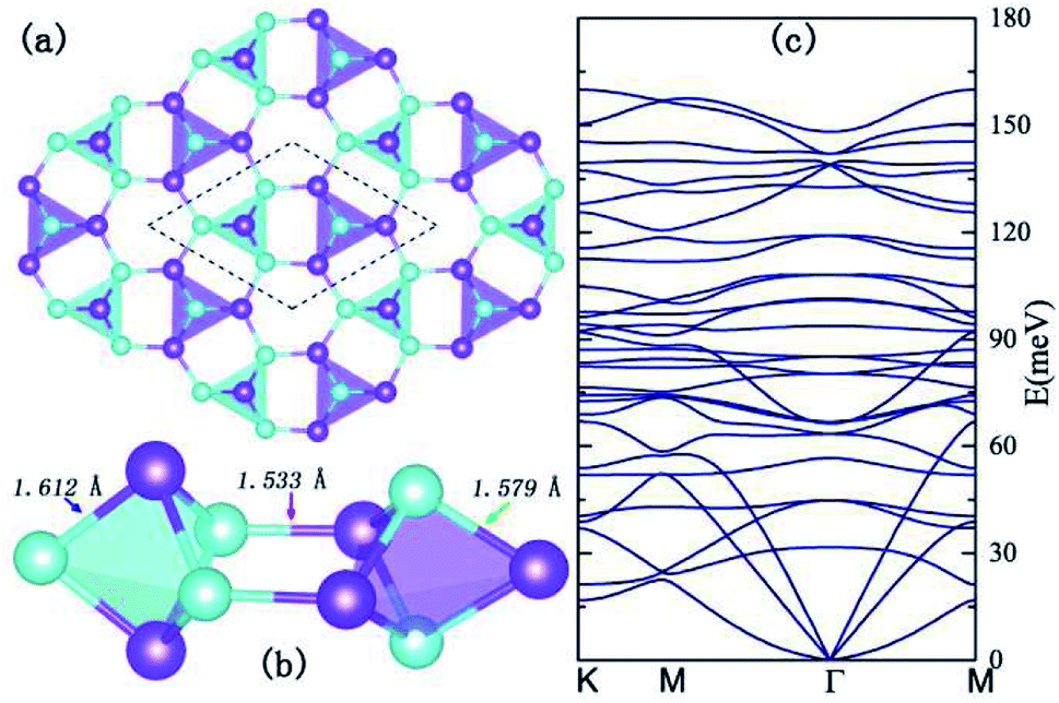
Inspired by the flat band induced s–p magnetism in graphene nanoribbons and artificially designed two-dimensional materials,28–30 we searched for 2D materials that possess flat bands which are protected by the crystal symmetries. To further enhance the magnetocrystalline anisotropy, in this work, we propose a new type of allotrope for h-BN with a decorated bounce lattice as shown in Fig. 1, since the 2-nd row elements boron and nitride behave like glue atoms and form versatile allotropes.31 The crystalline structure of the 2D B5N5 hosts the D3h symmetry with the space group P![[6 with combining macron]](https://www.rsc.org/images/entities/char_0036_0304.gif) m2 (no. 187), and possesses a trilayer configuration. In the middle of the trilayer, there lies a bounce lattice connecting adjacent boron and nitrogen equilateral triangles with a pair of B–N bonds, and the upper and lower layers possess a honeycomb lattice with boron and nitrogen atoms taking positions above and beneath the centers of the nitrogen and boron triangles alternatively, as illustrated in Fig. 1(a).
m2 (no. 187), and possesses a trilayer configuration. In the middle of the trilayer, there lies a bounce lattice connecting adjacent boron and nitrogen equilateral triangles with a pair of B–N bonds, and the upper and lower layers possess a honeycomb lattice with boron and nitrogen atoms taking positions above and beneath the centers of the nitrogen and boron triangles alternatively, as illustrated in Fig. 1(a).
 | ||
| Fig. 1 Crystal structure and stability. (a) Top-view of the B5N5 allotrope, the unitcell is indicate in the dashed area and the boron atoms and nitride atoms are indicated with purple and azure spheres, respectively. (b) The side view of the relaxed structure within a unitcell. (c) The phonon dispersions of the B5N5 monolayer in the Brillouin zone. | ||
The unitcell of this type of allotrope is indicated in Fig. 1(b) with dashed lines, and in each unitcell, there are two dual triangular bipyramids consisting of B3N2 and B2N3 clusters, respectively. Considering the unbalanced chemical compositions of the two bipyramids, structural distortions are expected and verified by structure relaxation. From Fig. 1(b), one can find out that the B2N3 and the B3N2 clusters are not symmetric, but shrink along horizontal and perpendicular directions, respectively. The fully relaxed lattice constant of the unitcell is a = b = 4.875 Å, and the lengths of the B–N bonds within the B2N3 and B3N2 clusters, and those bridging the two clusters are 1.612 Å, 1.579 Å, and 1.533 Å, respectively. To investigate the stability of the optimized crystal, we calculated the phonon dispersions by employing the frozen phonon method,32 and the phonon dispersions are shown in Fig. 1(c). No imaginary frequencies can be found throughout the whole Brillouin Zone (BZ) in phonon dispersions, indicating thermodynamic structural stability of the 2D structure. Therefore, we adopted the relaxed lattice parameters for all the subsequent calculations.
To calculate the electronic structures of this new type of monolayer allotrope, we set up a vacuum slab as thick as 20 Å, to ensure separation between adjacent monolayers to eliminate interlayer interactions, and perform the electronic structure calculations. The band structures of monolayer B5N5 in the vicinity of the Fermi level in the first BZ are shown in Fig. 2. From Fig. 2, one can see that the band gap is about 1.68 eV, and the highest valence band is nearly absolutely flat, with a bandwidth of about 20 meV. We analyse the orbital components of the flat band along a typical reciprocal path K–Γ–M, and denote each orbital with different coloured curves as displayed in Fig. 2(b), and the weight of each orbital is represented by the size of the corresponding circle. From Fig. 2(b), one can see that the s and pz orbitals are dominant in the flat band (the highest valence band), the lowest two conduction bands are almost pure pz and the second and third valence bands are comprised of almost equal px and py orbitals. The corresponding densities of states of orbitals are shown in Fig. 2(c), and are denoted by solid lines with the same colours as in Fig. 2(b).
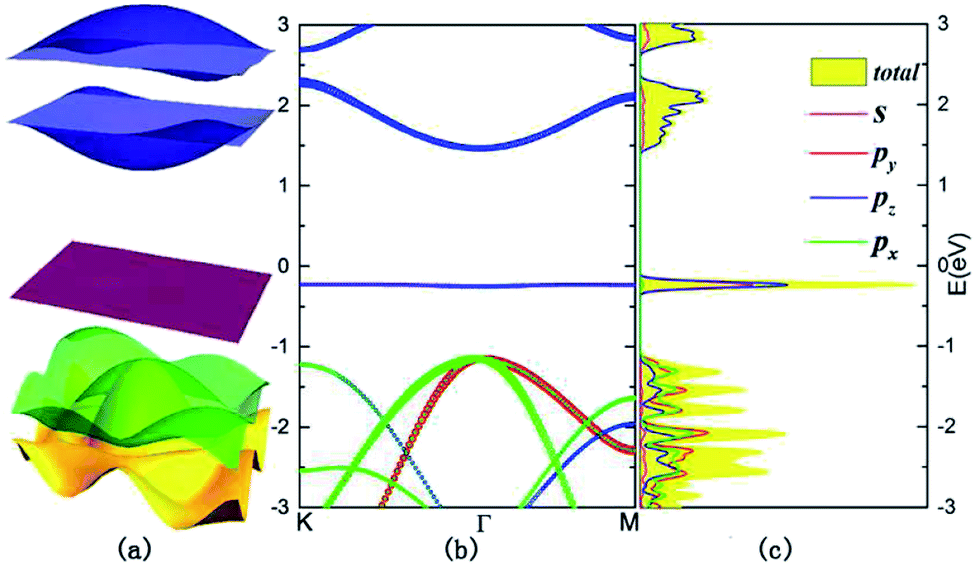 | ||
| Fig. 2 Electronic structures. (a) 3-D band structures of B5N5 within the first BZ. (b) The band structures of B5N5, the Fermi surface is set to be 0 and the orbital components are indicated by separate color circles, magenta for s, red for py, blue for pz, and green for px orbitals, respectively. (c) The densities of states (DOS) on the same energy scale as (b), the projected DOS are indicated by solid lines with the corresponding color codings. | ||
To clarify the origin of the flat band, we calculated its spatial charge distributions as illustrated in Fig. 3(b). From Fig. 3(b), it can be found that the wave functions of the flat band locate at the top and bottom boron atoms, and possess typical hybridized s–pz orbital characteristics. In such a nearly absolute flat band, the kinetic potentials of the carriers are almost quenched, and the electron correlations become more important. Spin polarized band structure calculations, as shown in Fig. 3(a), reveal that all the energy bands are doubly degenerate with anti-parallel spin states. However, the spatial distributions of opposite spins are separated. In Fig. 3(c), the upward and downward spins display intralayer ferromagnetic and interlayer antiferromagnetic orderings, making the monolayer B5N5 a 2D antiferromagnetic insulator.
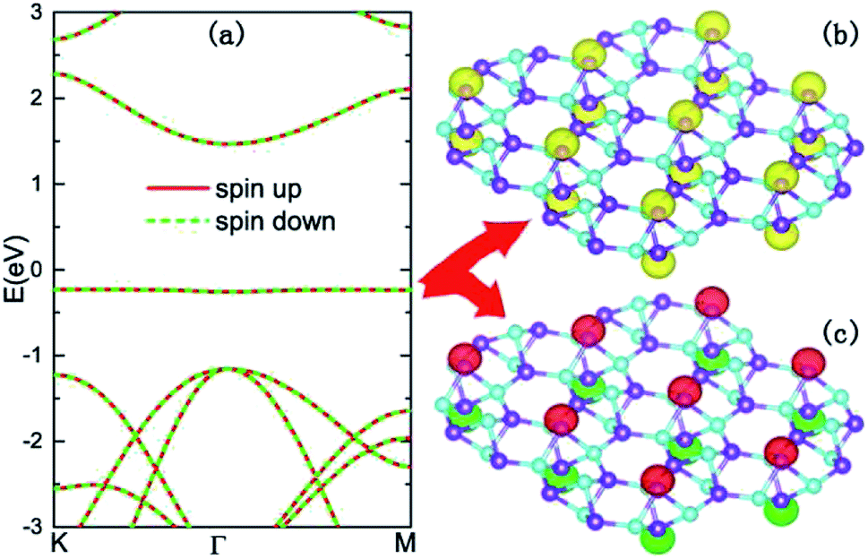 | ||
| Fig. 3 Antiferromagnetic insulator. (a) Spin polarized band structures of B5N5, the spin-up and spin-down dispersions are denoted with red solid lines and green dashed lines, respectively. (b) Spatial charge density distributions (yellow isosurfaces) of the flat-bands in the vicinity of the Fermi level. (c) Spatial spin density distributions of the spin-degenerate flat-bands, the spin-up and spin-down components are denoted with red and green isosurfaces, respectively. | ||
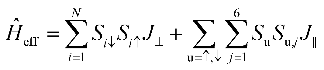
To demonstrate that the antiferromagnetic insulating phase is the ground state of B5N5, various calculations, such as the rotationally invariant DFT+U approach with a series of Hubbard U corrections up to 5 eV, and tunable exchange interactions within the HSE06 scheme are performed. The antiferromagnetic insulator feature remains unchanged (see ESI Part I†). The ground state possesses an A-type antiferromagnet and aligns perpendicular to the 2D material, and it can be conveniently described using an effective Hamiltonian as follows,
 | (1) |
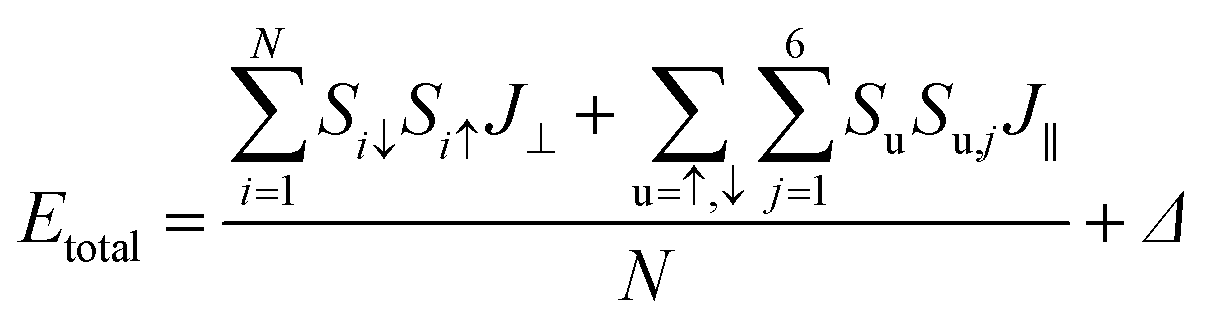
In order to determine quantitatively the magnetic exchange coupling parameters J⊥ and J∥, various magnetic orderings were studied based on constrained local spin density approximations (CLSDA),33 and Fig. 4 exhibits the relative total energy differences between the antiferromagnetic structure, ferromagnetic structure and two intermediate magnetic structures. To compare the total energy differences, the collinear magnetic structures are calculated and displayed with a 3 × 3 supercell. The antiferromagnetic structure has the minimal total energy with a 0 net magnetic moment, because the doubly degenerate flat band is occupied by two electrons with opposite spins as indicated by the density of states in the lower panel of Fig. 4. The ferromagnetic counterpart has the maximal total energy with a net magnetic moment of 2 μB. Since the spin densities of the two configurations are identical in magnitude, the net magnetic moment at the boron sites S is 1 μB, and shows intrinsic s–p electron magnetism. By constructing magnetic orderings with total energy differences, the magnetic exchange coupling parameters can be numerically derived by applying the following formula with the output of constrained DFT. The total energy of the studied magnetic orderings can be expressed as the formula as follows:
 | (2) |
 | ||
| Fig. 4 Antiferromagnetic insulator as the ground state. Total energy differences per atom between various magnetic structures. In the upper panel and from the left to right, the magnetic structures of antiferromagnetic, intermediate and ferromagnetic structures are displayed. The middle arrow indicates the increase of the energy differences. And the corresponding spin densities of states are illustrated in the lower panel. The spin-up and spin-down states are denoted with red and green color coding, respectively. | ||
The magnetic exchange coupling parameters J⊥ and J∥ are mapped and J⊥ = 76.7 meV and J∥ = −88.9 meV. The positive J⊥ and negative J∥ indicate the interlayer antiferromagnetic and intralayer ferromagnetic orderings of monolayer B5N5. With these parameters, the Néel temperature TN can be approximately estimated as 629.22 K by fitting the modified random phase approximation (RPA) like relation,34TN = −2πρs/[b − ln(−2J⊥/J∥)], where ρs = 0.183J∥, and b = 2.43 is an empirical constant. Although the mean-field approximation usually overestimates TN, the 2D antiferromagnet could be observed at room temperatures.
Antiferromagnetism surviving at room temperatures makes monolayer B5N5 a possible building block to construct flexible 2D spintronic devices. To mimic realistic interfacial conditions such as charge transfer induced electric fields and lattice-mismatch induced stress in van der Waals heterostructures, the electronic structures of B5N5 under external stress and electric fields were investigated. The responses of B5N5 to external biaxial stress are relatively complicated, where tensile biaxial stress enhances the interlayer coupling strength but weakens the intralayer coupling strength. In the reciprocal space, the second valence band is pushed away from the isolated flat band, and the magnetic structure remains an A-type antiferromagnetic insulator (intralayer ferromagnetic and interlayer antiferromagnetic). In contrast, compressive biaxial stress enhances the intralayer coupling but weakens the interlayer coupling, and mixed the px–py dominant valence band with the s–pz flat band. The band gap reduces significantly and the magnetic structure of the system changes to a G-type antiferromagnetic semiconductor (both intralayer and interlayer antiferromagnetic). The A-type to G-type phase transition at a critical compressive biaxial strain of about −3% and the evolution of band structures and spin orderings under compressive biaxial stress are exhibited (see ESI Part III†). Nevertheless the antiferromagnetic feature remains under both tensile and compressive stress.
Meanwhile perpendicular electric fields are effective to remove the degeneracy of the flat band (the dependency of band splitting on perpendicular electric fields is shown in ESI Part IV†), and separate the spin-up and spin-down channels without overlapping, and therefore a dual spin filter with high spin selectivity can be expected. The underlying physics comes from the feature of the flat bands, which are degenerate in the energy space while separated in the real space. In the presence of the vertical distance between the upper and lower boron sub-layers, a perpendicular electric field will induce an electrostatic potential between the states of opposite spins. As a consequence, perpendicular electric fields are effective to lift the two-fold degenerate flat bands, and drive the system into a half metallic phase.
A prototype dual spin filter device is shown in Fig. 5. In Fig. 5(a), two top gates are applied perpendicularly on the monolayer B5N5; the first gate V1 is responsible for separating spin-up and spin-down carriers, and the second gate V2 works as a spin valve to switch on or off the spin channels. When the directions of V1 and V2 are parallel/anti-parallel, the spin channels are switched on/off, and the dual spin filter works in the ON/OFF state, as illustrated in Fig. 5(b) and (c). In Fig. 5(b) and (c), red and green solid lines are energy dispersions all over the BZ of spin-up and spin-down carriers in the vicinity of the Fermi surface, and both the gate voltages are |V1| = |V2| = 3 V, and the energetic relative locations of spin-up and spin-down states can be switched by the direction of V1, which makes spin states tunable. Since the upper states possess a narrow band width, a perpendicular gate voltage exceeding 0.58 V can eliminate energy overlapping between opposite spin states, and the spin polarization of the current can be as high as nearly 100%.
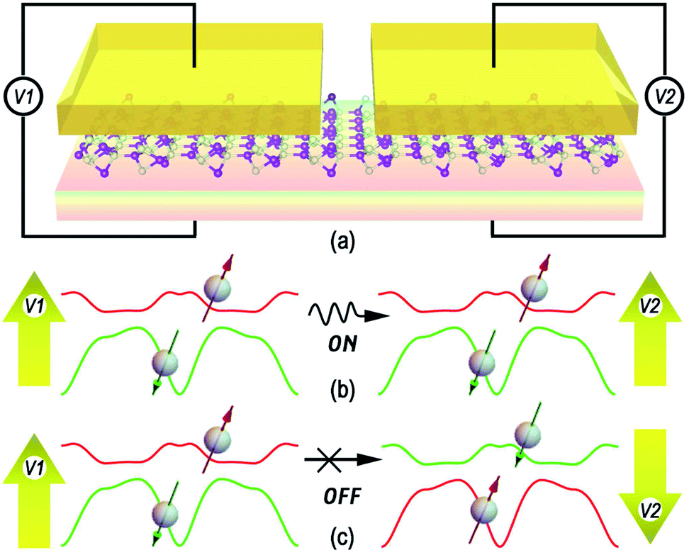 | ||
| Fig. 5 Dual spin filter. (a) Schematic of the dual spin filter based on monolayer B5N5, (b) on state and (c) off state of pure spin current obtained by applying parallel and anti-parallel voltages. Spin-up and spin-down states are denoted with red and green colour codings, respectively. | ||
3 Discussion
In recent years, antiferromagnets have been recognized as promising future spintronic materials rather than merely passive components in exchange bias applications. The renaissance of antiferromagnets is due to their advantageous properties such as insensitivity to external magnetic fields and high intrinsic frequency dynamics.35–37 Owing to the rapid progress of 2D spintronics, electrically tunable and robust monolayer antiferromagnets are of particular interest.In this work, we demonstrate that the intrinsic magnetic ordering survives even at room temperature in monolayer B5N5 with a decorated bounce lattice, which is a thermodynamically stable A-type 2D antiferromagnetic insulator. The antiferromagnetism in such a 2D material arises from the nearly flat bands in the vicinity of the Fermi energy, and is robust under external biaxial stress. A perpendicular electric field can remove the flat band degeneracy and a prototype dual spin filter is proposed. Our proposal not only offers a promising antiferromagnet candidate in the atomically-thin limit, but also provides an alternative way to explore antiferromagnetic insulators consisting of super-light and non-magnetic atoms.
4 Methods
Phonon dispersions are calculated with the PHONOPY code.38 Electronic structure calculations of B5N5 are performed by using the Vienna ab initio simulation package (VASP)39 within the screened-nonlocal exchange Heyd–Scuseria–Ernzerhof (HSE06)40 hybrid functional of the generalized Kohn–Sham scheme. The projector augmented-wave (PAW) pseudopotentials41 are adopted, and the kinetic energy cut-off is set to be 560 eV for wave-function expansions, and a Γ-centred k-point grid is densely sampled by summing over 13 × 13 × 1.42 Since both boron and nitride are super-light species with literally negligible intrinsic spin–orbit couplings (SOC), only the spin polarized band structure calculations are performed.Conflicts of interest
There are no conflicts to declare.Acknowledgements
This work was supported by the National Key R&D Programmes of China, Grant No. 2017YFA0303400, 2016YFE0110000, National Natural Science Foundation of China, Grant No. 11574303, 11504366, Youth Innovation Promotion Association of Chinese Academy of Sciences, Grant No. 2018148, and the Strategic Priority Research Program of Chinese Academy of Sciences, Grant No. XDB28000000. D. Zhang is thankful for the discussion with Prof. Xiong and inspiration from his beloved daughter, Miss 4D. Zhang.Notes and references
- R. Peierls, Math. Proc. Cambridge Philos. Soc., 1936, 477–481 CrossRef.
- N. D. Mermin and H. Wagner, Phys. Rev. Lett., 1966, 17, 1133 CrossRef CAS.
- L. Onsager, Phys. Rev., 1944, 65, 117 CrossRef CAS.
- C. T. Kuo, M. Neumann, K. Balamurugan, H. J. Park, S. Kang, H. W. Shiu, J. H. Kang, B. H. Hong, M. Han, T. W. Noh and J. G. Park, Sci. Rep., 2016, 6, 20904 CrossRef CAS PubMed.
- K. Z. Du, X. Z. Wang, Y. Liu, P. Hu, M. I. B. Utama, C. K. Gan, Q. Xiong and C. Kloc, ACS Nano, 2016, 10, 1738–1743 CrossRef CAS PubMed.
- J.-U. Lee, S. Lee, J. H. Ryoo, S. Kang, T. Y. Kim, P. Kim, C.-H. Park, J.-G. Park and H. Cheong, Nano Lett., 2016, 16, 7433–7438 CrossRef CAS PubMed.
- X. Wang, K. Du, Y. Y. F. Liu, P. Hu, J. Zhang, Q. Zhang, M. H. S. Owen, X. Lu, C. K. Gan, P. Sengupta, C. Kloc and Q. Xiong, 2D Mater., 2016, 3, 1–9 CAS.
- M. W. Lin, H. L. Zhuang, J. Yan, T. Z. Ward, A. A. Puretzky, C. M. Rouleau, Z. Gai, L. Liang, V. Meunier, B. G. Sumpter, P. Ganesh, P. R. Kent, D. B. Geohegan, D. G. Mandrus and K. Xiao, J. Mater. Chem. C, 2016, 4, 315–322 RSC.
- B. Huang, G. Clark, E. Navarro-Moratalla, D. R. Klein, R. Cheng, K. L. Seyler, D. Zhong, E. Schmidgall, M. A. McGuire, D. H. Cobden, W. Yao, D. Xiao, P. Jarillo-Herrero and X. Xu, Nature, 2017, 546, 270–273 CrossRef CAS PubMed.
- C. Gong, L. Li, Z. Li, H. Ji, A. Stern, Y. Xia, T. Cao, W. Bao, C. Wang, Y. Wang, Z. Q. Qiu, R. J. Cava, S. G. Louie, J. Xia and X. Zhang, Nature, 2017, 546, 265–269 CrossRef CAS PubMed.
- B. Chen, J. H. Yang, H. D. Wang, M. Imai, H. Ohta, C. Michioka, K. Yoshimura and M. H. Fang, J. Phys. Soc. Jpn., 2013, 82, 124711 CrossRef.
- Z. Fei, B. Huang, P. Malinowski, W. Wang, T. Song, J. Sanchez, W. Yao, D. Xiao, X. Zhu, A. F. May, W. Wu, D. H. Cobden, J. H. Chu and X. Xu, Nat. Mater., 2018, 17, 778–782 CrossRef CAS PubMed.
- Y. Deng, Y. Yu, Y. Song, J. Zhang, N. Z. Wang, Z. Sun, Y. Yi, Y. Z. Wu, S. Wu, J. Zhu, J. Wang, X. H. Chen and Y. Zhang, Nature, 2018, 563, 94–99 CrossRef CAS PubMed.
- M. Bonilla, S. Kolekar, Y. Ma, H. C. Diaz, V. Kalappattil, R. Das, T. Eggers, H. R. Gutierrez, M. H. Phan and M. Batzill, Nat. Nanotechnol., 2018, 13, 289–293 CrossRef CAS PubMed.
- D. J. O'Hara, T. Zhu, A. H. Trout, A. S. Ahmed, Y. K. Luo, C. H. Lee, M. R. Brenner, S. Rajan, J. A. Gupta, D. W. McComb and R. K. Kawakami, Nano Lett., 2018, 18, 3125–3131 CrossRef PubMed.
- M. Gibertini, M. Koperski, A. F. Morpurgo and K. S. Novoselov, Nat. Nanotechnol., 2019, 14, 408–419 CrossRef CAS PubMed.
- C. Gong and X. Zhang, Science, 2019, 363, eaav4450 CrossRef CAS PubMed.
- S.-J. Gong, C. Gong, Y.-Y. Sun, W.-Y. Tong, C.-G. Duan, J.-H. Chu and X. Zhang, Proc. Natl. Acad. Sci. U. S. A., 2018, 115, 8511–8516 CrossRef CAS PubMed.
- M. M. Ugeda, I. Brihuega, F. Guinea and J. M. Gómez-Rodríguez, Phys. Rev. Lett., 2010, 104, 096804 CrossRef CAS PubMed.
- J. Červenka, M. I. Katsnelson and C. F. Flipse, Nat. Phys., 2009, 5, 840–844 Search PubMed.
- B. Uchoa, V. N. Kotov, N. M. R. Peres and A. H. C. Neto, Phys. Rev. Lett., 2008, 101, 26805 CrossRef PubMed.
- R. R. Nair, M. Sepioni, I. L. Tsai, O. Lehtinen, J. Keinonen, A. V. Krasheninnikov, T. Thomson, A. K. Geim and I. V. Grigorieva, Nat. Phys., 2012, 8, 199–202 Search PubMed.
- Y. W. Son, M. L. Cohen and S. G. Louie, Nature, 2006, 444, 347–349 CrossRef CAS PubMed.
- J. Jung, T. Pereg-Barnea and A. H. Macdonald, Phys. Rev. Lett., 2009, 102, 227205 CrossRef CAS PubMed.
- D. Zhang, D.-B. Zhang, F. Yang, H.-Q. Lin, H. Xu and K. Chang, 2D Mater., 2015, 2, 041001 CrossRef.
- G. Z. Magda, X. Jin, I. Hagymási, P. Vancsó, Z. Osváth, P. Nemes-Incze, C. Hwang, L. P. Biró and L. Tapasztó, Nature, 2014, 514, 608–611 CrossRef CAS PubMed.
- M. Slota, A. Keerthi, W. K. Myers, E. Tretyakov, M. Baumgarten, A. Ardavan, H. Sadeghi, C. J. Lambert, A. Narita, K. Müllen and L. Bogani, Nature, 2018, 557, 691–695 CrossRef CAS PubMed.
- Z. Liu, Z.-F. Wang, J.-W. Mei, Y.-S. Wu and F. Liu, Phys. Rev. Lett., 2013, 110, 106804 CrossRef PubMed.
- M. Zhou, Z. Liu, W. Ming, Z. Wang and F. Liu, Phys. Rev. Lett., 2014, 113, 236802 CrossRef PubMed.
- P. Le, B. Hoi and M. Yarmohammadi, AIP Adv., 2018, 8, 125317 CrossRef.
- M. Shahrokhi, B. Mortazavi and G. R. Berdiyorov, Solid State Commun., 2017, 253, 51–56 CrossRef CAS.
- K. Parlinski, Z. Q. Li and Y. Kawazoe, Phys. Rev. Lett., 1997, 78, 4063–4066 CrossRef CAS.
- B. Kaduk, T. Kowalczyk and T. Van Voorhis, Chem. Rev., 2012, 112, 321–370 CrossRef CAS PubMed.
- C. Yasuda, K. Hukushima, F. Alet, M. Keller, M. Troyer and H. Takayama, Phys. Rev. Lett., 2005, 94, 217201 CrossRef CAS PubMed.
- V. Baltz, A. Manchon, M. Tsoi, T. Moriyama, T. Ono and Y. Tserkovnyak, Rev. Mod. Phys., 2018, 90, 015005 CrossRef CAS.
- M. B. Jungfleisch, W. Zhang and A. Hoffmann, Phys. Lett. A, 2018, 382, 865–871 CrossRef CAS.
- T. Jungwirth, J. Sinova, A. Manchon, X. Marti, J. Wunderlich and C. Felser, Nat. Phys., 2018, 14, 200–203 Search PubMed.
- A. Togo, F. Oba and I. Tanaka, Phys. Rev. B: Condens. Matter Mater. Phys., 2008, 78, 134106 CrossRef.
- G. Kresse and J. Furthmüller, Phys. Rev. B: Condens. Matter Mater. Phys., 1996, 54, 11169–11186 CrossRef CAS PubMed.
- J. Heyd, G. E. Scuseria and M. Ernzerhof, J. Chem. Phys., 2006, 124, 219906 CrossRef.
- P. E. Blöchl, Phys. Rev. B: Condens. Matter Mater. Phys., 1994, 50, 17953–17979 CrossRef PubMed.
- H. J. Monkhorst and J. D. Pack, Phys. Rev. B: Solid State, 1976, 13, 5188–5192 CrossRef.
Footnote |
| † Electronic supplementary information (ESI) available. See DOI: 10.1039/d0na00270d |
| This journal is © The Royal Society of Chemistry 2020 |