
 Open Access Article
 This Open Access Article is licensed under a Creative Commons Attribution-Non Commercial 3.0 Unported Licence
Small mode volume plasmonic film-coupled nanostar resonators
Negar
Charchi
a,
Ying
Li
b,
Margaret
Huber
a,
Elyahb Allie
Kwizera
c,
Xiaohua
Huang
 c,
Christos
Argyropoulos
*b and
Thang
Hoang
*a
c,
Christos
Argyropoulos
*b and
Thang
Hoang
*a
aDepartment of Physics and Materials Science, The University of Memphis, Memphis, TN 38152, USA. E-mail: tbhoang@memphis.edu
bDepartment of Electrical and Computer Engineering, University of Nebraska-Lincoln, Lincoln, NE 68588, USA. E-mail: christos.argyropoulos@unl.edu
cDepartment of Chemistry, The University of Memphis, Memphis, TN 38152, USA
First published on 4th May 2020
Abstract
Confining and controlling light in extreme subwavelength scales are tantalizing tasks. In this work, we report a study of individual plasmonic film-coupled nanostar resonators where polarized plasmonic optical modes are trapped in ultrasmall volumes. Individual gold nanostars, separated from a flat gold film by a thin dielectric spacer layer, exhibit a strong light confinement between the sub-10 nm volume of the nanostar's tips and the film. Through dark field scattering measurements of many individual nanostars, a statistical observation of the scattered spectra is obtained and compared with extensive simulation data to reveal the origins of the resonant peaks. We observe that an individual nanostar on a flat gold film can result in a resonant spectrum with single, double or multiple peaks. Further, these resonant peaks are strongly polarized under white light illumination. Our simulation data revealed that the resonant spectrum of an individual film-coupled nanostar resonator is related to the symmetry of the nanostar, as well as the orientation of the nanostar relative to its placement on the gold substrate. Our results demonstrate a simple new method to create an ultrasmall mode volume and polarization sensitive plasmonic platform which could be useful for applications in sensing or enhanced light–matter interactions.
1. Introduction
Attempts to create ultrasmall hot spots to confine light at the nanoscale have led to various nanophotonic system designs realized via both lithographic and colloidal approaches.1–9 Among these, plasmonic nanoparticles have proven to be an excellent platform to strongly confine light at length scales much smaller than the diffraction limit.4,10–13 As a general rule of thumb, the mode volume (or the hot spot) of a plasmonic nanoparticle is scaled with the size of the particle. Further, the resonant wavelength is also proportional to the size of the particle itself.4,10,11,14 This is generally correct for both nanoparticles, such as gold (Au) nanospheres or silver (Ag) nanocubes, in air and film-coupled. For instance, the resonant wavelengths of spherical Au nanoparticles occur between 550–800 nm for particle sizes ranging from 30–100 nm. Similarly, for Ag nanocubes with sizes varying from 50–150 nm, their gap mode resonant wavelengths change from around 600 nm to 1200 nm.4,10,14 However, smaller particle sizes (<30 nm) will limit the capability to perform dark-field spectroscopy of single particles due to the limited amount of scattered light and residual stray light. Therefore, the possibility of single particle identification is limited under a conventional dark-field illumination and the plasmonic hot spot volumes are usually in the order of a few tens of nanometers due to the relatively large particle sizes. Indeed, in order to study the optical response of very small (10–15 nm) plasmonic particles other techniques such as enhanced fluorescence or wide-field illumination and detection have been employed.15,16 Furthermore, structures such as nanospheres on mirror,1,11,12 could potentially provide small mode volumes but do not offer polarized optical modes, thus limiting the possibility of polarization control, which can be important for sensing and anisotropic emission applications. Elongated Au nanorod (with relatively large diameter of 45 nm) on mirror nanoantenna structure has been shown to offer anisotropic optical responses with potential applications in nanophotonics.17 Other lithographic techniques also attempted to create very small mode volume structures2,7 but the results are still limited to around 30 nm due to several limitations of conventional electron beam lithography systems. Recently, many works have devoted considerable attention to the optical properties of plasmonic nanostars,18–22 which have several advantageous characteristics. Unlike many other previously studied metallic nanoparticles with given symmetries, such as nanospheres23,24 or nanocubes,10,14 nanopopcorns25,26 and nanostars9,18–22,27–31 exhibit to a certain degree non-uniform distribution of localized plasmonic fields along their spikes or tips. Indeed, nanostars have recently attracted intensive attention in nanophotonics,21,22 biology,28,32–35 and materials science,5,36–39 thanks to their ability to localize electromagnetic fields in nanoscale hot spots at their highly engineered nanoscale tips. Several works related to the optical properties of Au nanostars have studied ensembles of particles5,27,28,40,41 which offered limited details regarding the mode resonances. Recently, several other works have also looked into the plasmon resonances of individual nanostars providing more details relating the optical properties with the nanoscale tips.9,18,29,30,42,43 Shao et al. have also reported optical properties of single nanostars on an indium tin oxide substrate.20Here, we demonstrate an alternative approach to confine plasmonic optical modes in ultrasmall volumes by using film-coupled nanostar resonators. Specifically, a Au nanostar is placed on top of a Au film, separated by a thin (5 nm) dielectric polymer layer. We show that the plasmon resonances of the nanostar's tips are significantly enhanced due to the resulted extreme sub-wavelength mode volume. Our results clearly indicate that the highly intense electromagnetic field enhancement in the small gaps formed between the nanostar's tips and the Au film can strongly confine light at a sub-10 nm volume. Moreover, the nanostars are relatively large (∼75 nm) therefore they are clearly visible under a typical dark field microscope, despite the ultrasmall mode volumes near their tips, allowing easy identification and measurement of single nanoparticles. Indeed, when illuminated by a white light source, the nanostars that are coupled to a Au film appear to be much brighter than the same particles that are deposited on a glass substrate. Furthermore, in contrast to previous works,1,10–12,14,44 the resonant modes of the film-coupled nanostar resonators are strongly polarized which offer an additional degree of freedom to control light at the nanoscale. The strong light–matter interactions achieved by the proposed plasmonic film-coupled nanostar platform can be used for sensing13 and to boost fluorescence anisotropy,45 or nonlinear46,47 and quantum5,48 optical applications.
2. Film-coupled nanostar resonators
The sample structure of this present study consists of colloidal synthesized iron oxide-gold core–shell nanostars with an approximate size of 75 nm placed over a Au film (50 nm thick, fabricated by electron beam evaporation method). The magnetic iron oxide core was about 35 nm and the Au shell layer was 40 nm. The iron oxide-gold core–shell nanostar's original purpose was to make use of its dual-functionality, namely magnetic and plasmonic properties, for biomedical applications.27 However, for this particular work the iron core's role was to serve as a catalyst for the nanostar growth and the core does not affect the plasmon resonant wavelengths of the Au nanostar. Kwizera and co-workers27,40 have previous shown that for the magnetic–plasmonic core–shell nanoparticles (including nanostars), when the Au shell thickness is larger than 15 nm, the change in the plasmonic resonant wavelength is negligible. Further, the tips of the nanostar (<10 nm) are pure Au so the plasmon resonances from the tips are not affected by the magnetic core. The core–shell Au nanostar and the Au film were separated by a 5 nm polymer spacer layer sandwiched in between (Fig. 1(a)).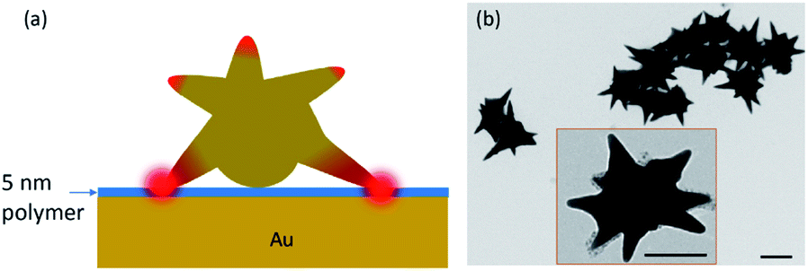 | ||
| Fig. 1 (a) Schematic of the proposed ultrasmall mode volume plasmonic film-coupled nanostar resonator: a nanostar with sub-10 nm tips situated on top of a Au film, separated by a very thin 5 nm polymer dielectric layer. (b) TEM image of typical nanostars. Inset: a close view of a single nanostar. Scale bars are 50 nm. | ||
The polymer spacer layer was formed by alternative dip coating with polyelectrolytes (PE).3 Specifically, five alternating positive PAH (poly(allylamine) hydrochloride) and negative PSS (polystyrenesulfonate) layers (1 nm each) were used. The thickness of the spacer layer may affect the resonant wavelength and the amplitude of the scattered light intensity of the coupled nanostar-film resonator, depending on the incident angle of the illuminated light.49 The spikes (or tips) of the Au nanostars were estimated, via Transmission Electron Microscopy (TEM) image (Fig. 1(b)), to be less than 10 nm. Indeed, the small tips of the nanostar permit the formation of nanoscale hot spots. The deposition technique of nanostars on a Au film was described elsewhere3 and the surface coverage of nanostars was less than 5% (Fig. 2).
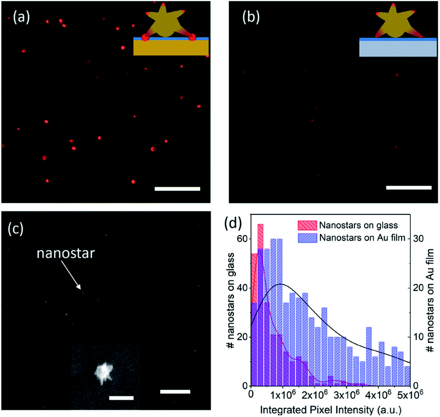 | ||
| Fig. 2 Dark-field scattering and SEM studies. (a) Dark-field image of nanostars on a Au film and (b) on glass substrate. Both (a and b) were plotted by using the same brightness scale. (c) SEM image of the nanostars on a Au film substrate. Inset: a close view of a single nanostar on the Au film (scale bars in (a–c) are 1 μm, 100 nm for the inset). (d) Integrated pixels' intensity of the CCD images for nanostars on a Au film (blue) and on a glass substrate (red). Solid curves represent the intensity distributions. | ||
In the experimental procedure, individual nanostars were identified and isolated by a set of lenses and pinholes to allow single particle measurements. Specifically, individual nanostars were illuminated by a white light source through a 100× Nikon objective lens (numerical aperture NA = 0.9, 1 mm working distance) operating in the dark field mode. The scattered light from particles was collected by the same objective, filtered by a pinhole aperture, refocused onto the entrance slit of a spectrometer (Horiba Jobin-Yvon iHR550) and analysed by a CCD (Charged-Coupled Device) camera (Horiba Jobin-Yvon Synapse). For the TE (transverse electric) and TM (transverse magnetic) polarized light, our customized optical setup allowed for a rotatable linear polarizer to be placed in a microscope slider or on the optical path in free space so a polarized incident light can be achieved. The final scattering spectrum of a particular particle was normalized as  where INS, ISS, IWL and Idark are the light intensities measured from the nanostar, substrate, white light standard reflection piece, and the CCD dark counts, respectively. For better visualization (Fig. 2(a) and(b)) and for scattering intensity analysis (Fig. 2(c)), the nanostar scattering images were captured by a colour camera (Thorlabs DCC1645C) and by a high dynamic range black and white camera (Photometrics CoolSnap DYNO).
3. Experimental results
Fig. 2(a) and (b) show the dark field scattering colour images of Au nanostars for two different cases: on a flat Au film and on a glass substrate, respectively. Individual Au nanostars are visible as bright, red dots. For both cases, an identical 5 nm thin polymer layer was coated on the Au film or glass substrate prior to the nanostar deposition. Due to the random distribution of the nanostars on a given substrate (Au or glass), it is not simple to compare the resonant characteristics of individual nanostars with different polymer layer gap thicknesses. A previous computational study by Solís et al.49 has shown that depending on the incident angle of the illumination the thickness of the gap may have an effect on the spectral characteristics as well as the amplitude of the resonant peaks. In our optical measurements, because the nanostars' orientations were random, the incident angle of the illumination could vary from one to another. Therefore, throughout this work we used a fixed polymer gap thickness of 5 nm to limit the number of involved parameters. It can be clearly seen that the nanostars on a Au film in Fig. 2(a) are much brighter compared to similar stars on a glass substrate (Fig. 2(b)). This indicates that the nanostars have coupled with the underneath Au film and resulted in a strong plasmonic resonance response. Furthermore, in order to confirm the individual bright scattering dots shown in Fig. 2(a) and (b) are from individual nanostars, Fig. 2(c) shows a scanning electron microscope (SEM) image of nanostars on a Au film. Even though the SEM image cannot reveal detail of individual nanostar's tip (inset of Fig. 2(c)), it is clear that the nanoparticles were well separated and did not form clusters. Further, we believe that the distribution of the nanostars on a glass sample is the same as on a Au film sample, because in both cases the surface of the samples were coated with an identical 5 nm PE spacer layer. The images presented in Fig. 2(a) and (b) were captured by a colour camera that has a 255-pixel depth for each colour (red, green, and blue) and is only sensitive in the visible frequency range. In order to get the true image intensity from near UV to near IR (400–1050), we used another black and white CCD camera to take images of the nanostars for both cases. Fig. 2(d) shows the histogram of the integrated scattering intensity of individual nanostars for both samples. Each intensity value of an individual nanostar was integrated over an area of 20 × 20 pixels of the camera image. It is clear that the intensity from the film-coupled nanostar resonators is much brighter compared with the nanostars on a glass substrate.Fig. 3 shows the scattering spectra for individual nanostars on a Au film (Fig. 3(a) and (b)) and on a glass substrate (Fig. 3(c) and (d)). Due to the fact that the deposited nanostars on a surface were randomly distributed, the localized surface plasmon resonances will strongly depend on how an individual nanostar is oriented on the surface.18,20,42 As shown in Fig. 3, our measurements indicate that the resonant spectra of individual nanostars can be categorized into two main groups, those with single (Fig. 3(a) and (c)) and double (Fig. 3(b) and (d)) resonant peaks. For each sample, i.e. on glass or on Au film substrate, we have measured more than one hundred individual particles to draw this conclusion. During several occasions, we also observed resonant spectra with multiple (more than two) plasmon resonances. Previous studies9,18,41,42 have also observed similar resonant features for the case of nanostars in air. For instance, de Puig et al.41 have demonstrated the multimodal plasmon resonances of Au nanostars with various tip lengths. A recent work by Tsoulos et al.30 had a closer look at the optical properties of Au nanostars by combining experimental and 3D computational studies and relates the heat loss, plasmon resonances with the nanostar's orientation. However, in contrast to these previous works, our case has the existence of the Au film in close proximity to the tips of the nanostars, which helps to drastically enhance the mode confinement at the bottom tips.
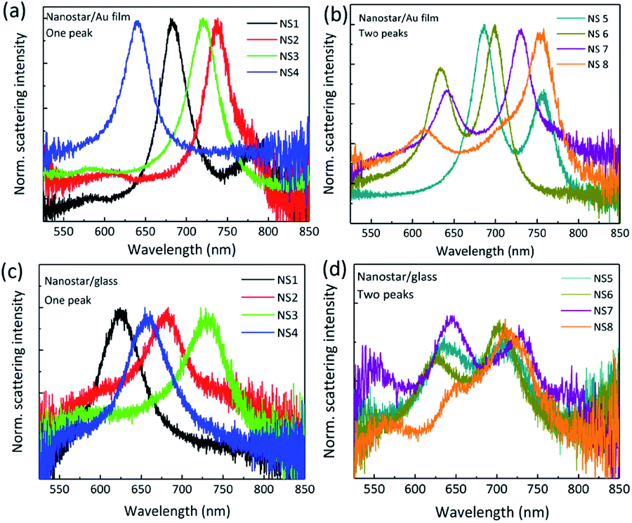 | ||
| Fig. 3 (a and b) Measured scattering spectra from individual nanostars on a Au film. Each panel represents a different group of spectral characteristics. (c and d) Similar measurements but for nanostars on a glass substrate. | ||
It is also noticed that for the nanostars on a Au film the spectral full width at half maximum (FWHM) of the plasmon resonances was narrower compared with the FWHM for the nanostars on a glass substrate. Specifically, for the nanostars on a Au film with a single resonant peak the average of measured FWHMs was 35.7 nm while for the nanostars on a glass substrate the averaged FWHMs was 55 nm. For the nanostars on a Au film that exhibited double resonant peaks the average of measured FWHMs were 32.5 nm and 32.0 nm for the lower and longer wavelength resonant peaks, respectively. On a glass substrate, these values were 48 nm and 47 nm for the lower and longer wavelength resonant peaks, respectively. As we have mentioned above the spectral characteristics of an individual nanostar resonator may vary depending on the orientation of the nanoparticle and the illumination condition. Nevertheless, our statistical data indicates a strong light confinement by the nanostars on the Au film. Furthermore, the spectral characteristics of the film-coupled Au nanostars presented in our current work are different compared to other film-coupled nanoparticle resonators, such as nanospheres1,11,12 and nanocubes,4,10 where only a single peak was observed. As we will be discussing below, the appearance of a single peak or double peaks in the resonant spectrum is closely related to the geometry of the nanostar and how the nanostar contacts with the substrate.
The results presented in Fig. 3(a) and (c) may indicate that the measured spectra were from nanostars with poorly formed tips.42 However, in such a situation one would expect an unpolarized resonant spectrum for a given particle due to its less asymmetrical shape. This is not always the case in our observations. In Fig. 4 we show the polarization excitation dependent measurements of individual nanostars on Au film for two different cases: single and double peaks. In the case of the single peak, the TE and TM polarized components resulted in a degree of polarization of P = 28.7%. Here, TE and TM polarized waves were chosen to be perpendicular to each other and the polarization degree was defined as  , where ITE and ITM are the scattering intensities for TE and TM signal, respectively. For the two-peak resonance case, the degrees of polarization were P = 61% and P = 86% for the 687 nm and 758 nm resonant peak, respectively. Previous studies by Hrelescu,9 Hao,18 and Nehl42 have also observed a similar polarization behaviour in the individual nanostar's scattering spectrum, which was related to the different tip geometries in these nanoparticles. Thus, these measurements allow us to conclude that the collected signal was from star-shaped nanoparticles.
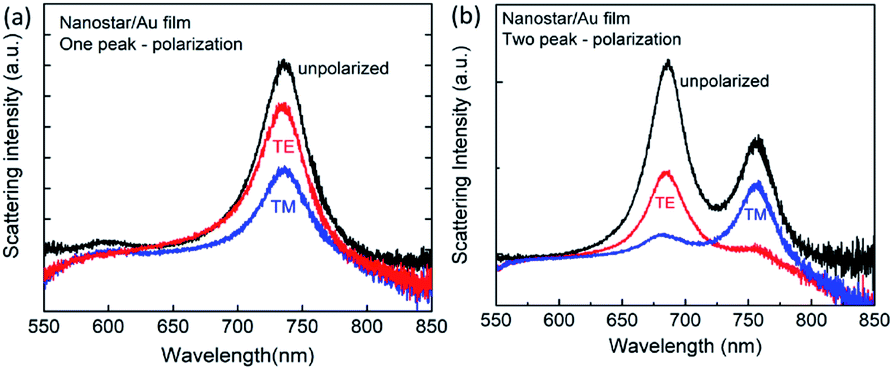 | ||
| Fig. 4 Scattering spectra detected for TE and TM polarization components for (a) single peak and (b) two peaks cases. | ||
4. Computational results
The deposited nanostars on a Au substrate can take random positions. In an ideal situation, one can label the position of a nanostar, measure its scattering spectrum and then proceed with a SEM measurement of the same particle.44Via this way, one can correlate the geometry of the film coupled nanostar resonator with the optical property of the same particle. However, our current SEM capability does not offer a high enough resolution to observe a single nanostar and its tip orientations and therefore does not allow us to follow this measurement approach. Therefore, we must turn our attention to computer simulations. We use the commercial finite-element simulation software Comsol Multiphysics to model several geometries that would represent possible experimental scenarios, including asymmetric properties, number of tips that touch the bottom film, and the polarizations of the scattered light from individual nanostars. Fig. 5 shows the simulated extinction spectra for nanostars at several different configurations and geometries placed on a Au film. The model is composed of four domains: metallic nano-star at the origin, free space surrounding the particle, polymer spacing layer (5 nm thickness) under the particle, and underlying Au substrate. In order to calculate the extinction cross section (ECS) of the film-coupled nanostars, we employ the scattered-field formulation that directly computes the scattered fields by subtracting the analytical solution of an incident plane wave in the absence of the nanostars, which is considered to be the background field.47 Perfectly matched layer (PML) boundary conditions are used outside the simulated spherical area to completely truncate the computation domain and absorb the scattered energy. The dimensions and geometries of the nanostars were extracted from the actual shapes of the particles taken from the TEM images, as shown in Fig. 1(b). For simplicity, we first consider a nanostar that has 12 relatively short and equal-length sharp tips branching out from a central spherical core. However, as observed from the experimental results of the TEM measurements, the nanostars' tips were not necessarily uniformly distributed around the bulk of the particle. In our first initial calculations, we assumed that the 12 tips are uniformly distributed around the central core resulting in a star-like dodecahedral gold nanocrystal and such nanostar has only one tip touching the bottom surface. The core diameter is around 75 nm and the tip length is about 30 nm. Each tip has corn shape with small apex (∼3 nm) and 34–52° corn angle. Fig. 5(a) shows the polarized (TE and TM) and unpolarized extinction spectra for this specific situation. The dielectric function of Au used in the simulations was taken from experimental data.50 A thin 5 nm polymer layer was placed in the nanogap with refractive index n = 1.4, which is identical to the thin polymer layer used in the experiment. The discretization of the simulation space is performed using the built-in free meshing Comsol algorithm, which uses a division into tetrahedral finite elements in the areas of the nanoparticle and surrounding medium. The PML thickness is selected in order to fully absorb each wavelength of the incident wave. The area of PML is divided into 5 spherical layers by using the sweep mesh function in Comsol with spherical symmetry. The maximum element size inside the nanoparticle is chosen to be 30 nm, related to the skin depth of the materials used. In terms of the surrounding medium, the maximum element size does not need to be so small, and is chosen as λ/6 in order to properly account for the changes in electric field. The ECS is calculated as the sum of the scattering and absorption spectra. The result of this particular simulation matches well with the measurement scattering spectra presented in Fig. 3(a) and 4(a). The TE and TM polarized waves in the simulation were perpendicular to each other. After checking the field enhancement distribution for each polarization illumination, we find that a strong plasmonic gap mode can be excited only under TM polarization illumination and no gap enhancement exists with TE polarization incidence. In addition, the incidence angle for this case is 45°, because the symmetric nanostar under normal illumination will not exhibit a plasmonic gap mode inside the thin (5 nm) polymer dielectric layer. This has also been demonstrated by Solís et al.49 However, after we introduce some asymmetry in the nanostructure, such as elongating either one or two of the asymmetric tips, a strong gap field enhancement can be achieved for both TE and TM polarization even under normal incidence illumination. We also study the cases when the nanostar has one and two asymmetric tips touching the surface under a normal incident illumination. For these scenarios, we observed two distinct peaks in the resonant spectra, which are indeed polarized differently for TE and TM illuminations. These later configurations result in an excellent agreement with the measured data presented in Fig. 3(b) and 4(b).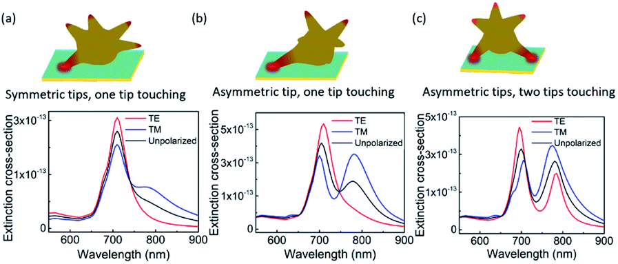 | ||
| Fig. 5 Simulated extinction spectra for three different geometries as schematically shown in the top row: (a) a single equal-length tip touches the substrate, (b) one asymmetric tip touches the substrate, and (c) two asymmetric tips touch the substrate. | ||
The associated field enhancement distributions of the resonant spectra in Fig. 5 are computed and shown in Fig. 6. We find that the symmetric nanostar under TE polarization illumination will not exhibit a plasmonic gap mode inside the thin polymer dielectric layer. In order to produce strong gap plasmonic mode enhancement, additional asymmetric nanostar configurations such as one elongating tip or two tips of the nanostars touching the polymer layer surface were introduced. Such asymmetries will resemble the experimentally observed TEM image of these nanostars (Fig. 1(b)). Fig. 6(a1) and (a2) show the normalized electric field distribution in the case of symmetric tips in the one tip touching geometry under different polarization illuminations (TE or TM) by using 45° incidence angle. It is clear that a strong plasmonic gap mode can be excited only under TM polarization illumination. Fig. 6(b1)–(b4) show four different field enhancement distributions in the case of one asymmetric tip, two tips touching nanostar, with geometry shown in Fig. 5(c). Specifically, Fig. 6(b1) and (b2) correspond to two ECS peaks when the nanostar is illuminated by TE polarization, Fig. 6(b3) and (b4) correspond to the other two resonance peaks under TM polarization. We find that the value of the field enhancement nearly doubles for the case of asymmetric tips geometry even under normal incidence illumination (Fig. 6(b)), compared to the field enhancement using only symmetric nanostar (Fig. 6(a)). Furthermore, we note that at the second resonant wavelength (∼780 nm), a strong plasmonic gap mode always exists under both TE (Fig. 6(b2)) and TM (Fig. 6(b4)) polarization incidence, which is different from the symmetric nanostar's response.
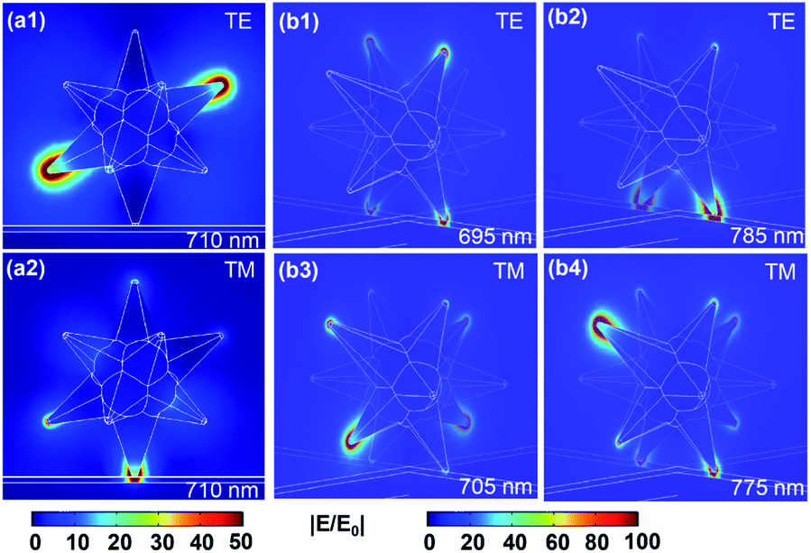 | ||
| Fig. 6 Normalized field distribution for two different geometries with different resonant wavelengths. (a1 and a2) Correspond to the geometry of symmetric tips, i.e., one tip touching nanostar, and (b1–b4) correspond to the case of asymmetric tip, i.e., two tips touching nanostar. | ||
We also note that there is a small wavelength offset between the computational data (Fig. 5) and the experimental data shown in Fig. 3 and 4. Indeed, in the experimental data there was quite a broad range of resonant wavelengths observed because the nanostars were randomly distributed as well as they were different in size. Therefore, the simulation data shown in Fig. 5 demonstrates the polarization properties of these film-coupled nanostars, which are in relative agreement with the experimental data. Additional simulation data to further explain this wavelength offset is shown in Fig. 7. In Fig. 7, we present some simulation results of a parametric study by changing the dimensions or shape (one tip or two tips touching or symmetric/asymmetric designs) of the nanostar. The simulated extinction spectra for different nanostar sizes match well with the measured scattering spectra presented in Fig. 3 above, where some nanostars have single (Fig. 7(a)) and others have double (Fig. 7(b)) resonant peaks. It is challenging to directly compare the results presented in Fig. 7 with the measured spectra in Fig. 3 because we do not know the exact orientations of the nanostars that were experimentally measured by our dark field scattering study. However, the results presented in Fig. 7 help us to understand that the resonant wavelength and spectral characteristics of each nanostar vary by using different geometries and shapes of the nanostar located on a Au film. These theoretical results are consistent with the variety of the measured scattering spectra presented in Fig. 3.
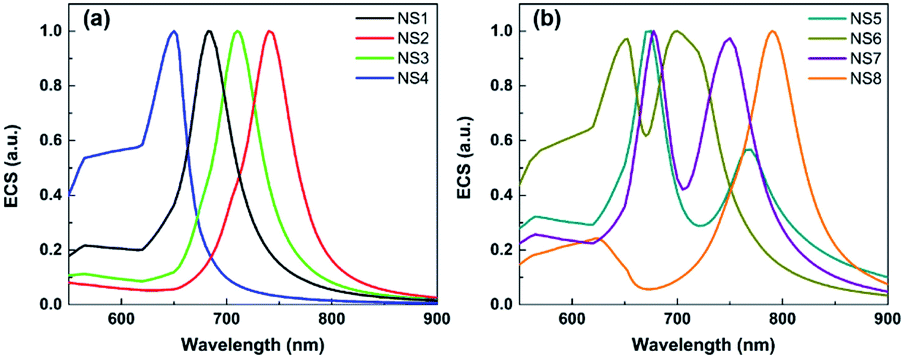 | ||
| Fig. 7 Simulated extinction spectra for several different geometries and shapes of nanostars located on a Au film. (a) Single resonant peak and (b) two resonant peaks cases. | ||
We also compute and present in Table 1 the estimated mode volume Veff of the plasmonic resonance modes in the three different geometries shown in Fig. 5(a)–(c). The mode volume is defined as 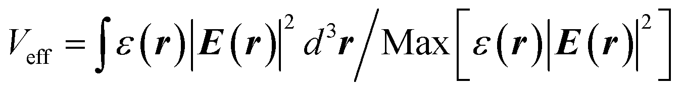 , where ε(r) is the material permittivity and the integration is performed over and around the mode's bright spot.51 From the above equation, the mode volume is characterized as the ratio of total electric energy to the maximum value of the electric energy density, where the maximum electric energy densities in our system are located around the nanoscale gaps formed between the nanostar's tips and Au film. The results in Table 1 show that a sub-10 nm mode volume can be achieved for both TE and TM polarization illuminations, especially in the case of the nanostar geometry with two asymmetric tips touching the bottom substrate (Table 1(c) and Fig. 6(b2) and (b4)). Compared to the configurations of one tip touching, the maximum electric filed enhancement is increased in the case of two tips touching. Several previous works have also demonstrated very small mode volumes for plasmonic platforms. For instance, Huang et al.1 have reported a computational work to demonstrate a nanoparticle – on – mirror structure that offers a mode volume below 10−7λ3. Other experimental works have also demonstrated 10−5λ3 plasmonic mode volume.2,6 Our method provides a quick and straightforward approach to create ultrasmall mode volume (considering the case of Fig. 5(c)) plasmonic nanocavities without the need for complicated electron lithography procedures. More importantly, the presented film-coupled nanostar resonator platform provides a pathway to control the light polarization at the nanoscale.
| V eff (nm3) | (a) | (b) | (c) |
|---|---|---|---|
| TE | 2.30 × 10⁻⁵λ3 | 1.62 × 10⁻⁵λ3 | 1.05 × 10⁻⁷λ3 |
| TM | 2.46 × 10⁻⁶λ3 | 1.81 × 10⁻⁵λ3 | 9.75 × 10⁻⁷λ3 |
5. Conclusions
In conclusion, we have investigated a film-coupled nanostar resonator system that offers extreme sub-wavelength mode volumes. It is demonstrated that by placing a Au nanostar on a flat Au film, ultrasmall mode volumes are formed and strong polarized light confinement is achieved in between the nanostar's tip and the film region. We have performed simulations to correlate the plasmonic resonant features with the geometry of the resonators by considering the asymmetric shape of the nanostar and how it may orient with respect to the underneath film. The film-coupled nanostar resonators provide a new approach to achieve strongly polarized light confinement within sub-10 nm mode volumes, which makes them an ideal platform for applications requiring enhanced light–matter interactions at low dimensions.Conflicts of interest
There are no conflicts to declare.Acknowledgements
This work was supported by the National Science Foundation (NSF) (Grant # DMR-1709612). TH acknowledges the Ralph E. Powe Junior Faculty Enhancement Award from Oak Ridge Associated Universities and FedEx Institute of Technology at the University of Memphis. XH acknowledges the support from the National Institutes of Health (Grant No. 1R15 CA 195509-01) and the Fedex Institute of Technology at the University of Memphis.References
- S. Huang, T. Ming, Y. Lin, X. Ling, Q. Ruan, T. Palacios, J. Wang, M. Dresselhaus and J. Kong, Small, 2016, 12, 5190–5199 CrossRef CAS PubMed.
- M. Kuttge, F. J. García de Abajo and A. Polman, Nano Lett., 2010, 10, 1537–1541 CrossRef CAS PubMed.
- T. B. Hoang, J. Huang and M. H. Mikkelsen, J. Visualized Exp., 2016, 111, e53876 Search PubMed.
- T. B. Hoang, G. M. Akselrod, C. Argyropoulos, J. Huang, D. R. Smith and M. H. Mikkelsen, Nat. Commun., 2015, 6, 7788 CrossRef CAS PubMed.
- H. Asgar, L. Jacob and T. B. Hoang, J. Appl. Phys., 2018, 124, 103105 CrossRef.
- H. Choi, M. Heuck and D. Englund, Phys. Rev. Lett., 2017, 118, 223605 CrossRef PubMed.
- A. Kinkhabwala, Z. Yu, S. Fan, Y. Avlasevich, K. Müllen and W. E. Moerner, Nat. Photonics, 2009, 3, 654 CrossRef CAS.
- E. B. Ureña, M. P. Kreuzer, S. Itzhakov, H. Rigneault, R. Quidant, D. Oron and J. Wenger, Adv. Mater., 2012, 24, OP314–OP320 CrossRef PubMed.
- C. Hrelescu, T. K. Sau, A. L. Rogach, F. Jäckel and J. Feldmann, Appl. Phys. Lett., 2009, 94, 153113 CrossRef.
- J. B. Lassiter, F. McGuire, J. J. Mock, C. Ciracì, R. T. Hill, B. J. Wiley, A. Chilkoti and D. R. Smith, Nano Lett., 2013, 13, 5866–5872 CrossRef CAS PubMed.
- C. Ciracì, R. T. Hill, J. J. Mock, Y. Urzhumov, A. I. Fernández-Domínguez, S. A. Maier, J. B. Pendry, A. Chilkoti and D. R. Smith, Science, 2012, 337, 1072 CrossRef PubMed.
- J. J. Mock, R. T. Hill, A. Degiron, S. Zauscher, A. Chilkoti and D. R. Smith, Nano Lett., 2008, 8, 2245–2252 CrossRef CAS PubMed.
- J. J. Baumberg, J. Aizpurua, M. H. Mikkelsen and D. R. Smith, Nat. Mater., 2019, 18, 668–678 CrossRef CAS PubMed.
- A. Moreau, C. Ciracì, J. J. Mock, R. T. Hill, Q. Wang, B. J. Wiley, A. Chilkoti and D. R. Smith, Nature, 2012, 492, 86 CrossRef CAS PubMed.
- A. Weigel, A. Sebesta and P. Kukura, ACS Photonics, 2014, 1, 848–856 CrossRef CAS.
- D. Melnikau, R. Esteban, D. Savateeva, A. Sánchez-Iglesias, M. Grzelczak, M. K. Schmidt, L. M. Liz-Marzán, J. Aizpurua and Y. P. Rakovich, J. Phys. Chem. Lett., 2016, 7, 354–362 CrossRef CAS PubMed.
- H. Sugimoto, S. Yashima and M. Fujii, ACS Photonics, 2018, 5, 3421–3427 CrossRef.
- F. Hao, C. L. Nehl, J. H. Hafner and P. Nordlander, Nano Lett., 2007, 7, 729–732 CrossRef CAS PubMed.
- K. Pandian Senthil, P.-S. Isabel, R.-G. Benito, F. J. G. d. Abajo and M. L.-M. Luis, Nanotechnolog, 2008, 19, 015606 CrossRef PubMed.
- L. Shao, A. S. Susha, L. S. Cheung, T. K. Sau, A. L. Rogach and J. Wang, Langmuir, 2012, 28, 8979–8984 CrossRef CAS PubMed.
- J. Ziegler, C. Wörister, C. Vidal, C. Hrelescu and T. A. Klar, ACS Photonics, 2016, 3, 919–923 CrossRef CAS PubMed.
- A. Kedia and P. S. Kumar, AIP Conf. Proc., 2013, 1512, 232–233 CrossRef CAS.
- F. Tam, G. P. Goodrich, B. R. Johnson and N. J. Halas, Nano Lett., 2007, 7, 496–501 CrossRef CAS PubMed.
- M. Hu, J. Chen, Z.-Y. Li, L. Au, G. V. Hartland, X. Li, M. Marquez and Y. Xia, Chem. Soc. Rev., 2006, 35, 1084–1094 RSC.
- Z. Fan, D. Senapati, A. Khan Sadia, K. Singh Anant, A. Hamme, B. Yust, D. Sardar and C. Ray Paresh, Chem.–Eur. J., 2013, 19, 2839–2847 CrossRef CAS PubMed.
- W. Lu, A. K. Singh, S. A. Khan, D. Senapati, H. Yu and P. C. Ray, J. Am. Chem. Soc., 2010, 132, 18103–18114 CrossRef CAS PubMed.
- E. A. Kwizera, E. Chaffin, X. Shen, J. Chen, Q. Zou, Z. Wu, Z. Gai, S. Bhana, R. O'Connor, L. Wang, H. Adhikari, S. R. Mishra, Y. Wang and X. Huang, J. Phys. Chem. C, 2016, 120, 10530–10546 CrossRef CAS PubMed.
- Y. Liu, H. Yuan, R. F. Kersey, K. J. Register, C. M. Parrott and T. Vo-Dinh, Sensors, 2015, 15, 3706–3720 CrossRef CAS PubMed.
- D. A. Wheeler, T. D. Green, H. Wang, C. Fernández-López, L. Liz-Marzán, S. Zou, K. L. Knappenberger and J. Z. Zhang, Chem. Phys. Lett., 2012, 543, 127–132 CrossRef CAS.
- T. V. Tsoulos, L. Han, J. Weir, H. L. Xin and L. Fabris, Nanoscale, 2017, 9, 3766–3773 RSC.
- A. S. De Silva Indrasekara, S. F. Johnson, R. A. Odion and T. Vo-Dinh, ACS Omega, 2018, 3, 2202–2210 CrossRef CAS PubMed.
- V. Raghavan, C. O'Flatharta, R. Dwyer, A. Breathnach, H. Zafar, P. Dockery, A. Wheatley, I. Keogh, M. Leahy and M. Olivo, Nanomedicine, 2017, 12, 457–471 CrossRef CAS PubMed.
- I. G. Theodorou, Q. Jiang, L. Malms, X. Xie, R. C. Coombes, E. O. Aboagye, A. E. Porter, M. P. Ryan and F. Xie, Nanoscale, 2018, 10, 15854–15864 RSC.
- S. K. Dondapati, T. K. Sau, C. Hrelescu, T. A. Klar, F. D. Stefani and J. Feldmann, ACS Nano, 2010, 4, 6318–6322 CrossRef CAS PubMed.
- S. M. Mousavi, M. Zarei, S. A. Hashemi, S. Ramakrishna, W.-H. Chiang, C. W. Lai and A. Gholami, Drug Metab. Rev., 2020, 1–20, DOI:10.1080/03602532.2020.1734021.
- X.-L. Liu, J.-H. Wang, S. Liang, D.-J. Yang, F. Nan, S.-J. Ding, L. Zhou, Z.-H. Hao and Q.-Q. Wang, J. Phys. Chem. C, 2014, 118, 9659–9664 CrossRef CAS.
- B. Munkhbat, J. Ziegler, H. Pöhl, C. Wörister, D. Sivun, M. C. Scharber, T. A. Klar and C. Hrelescu, J. Phys. Chem. C, 2016, 120, 23707–23715 CrossRef CAS PubMed.
- E. S. Kooij, W. Ahmed, C. Hellenthal, H. J. W. Zandvliet and B. Poelsema, Colloids Surf., A, 2012, 413, 231–238 CrossRef CAS.
- E. Nalbant Esenturk and A. R. Hight Walker, J. Raman Spectrosc., 2009, 40, 86–91 CrossRef.
- E. A. Kwizera, E. Chaffin, Y. Wang and X. Huang, RSC Adv., 2017, 7, 17137–17153 RSC.
- H. de Puig, J. O. Tam, C.-W. Yen, L. Gehrke and K. Hamad-Schifferli, J. Phys. Chem. C, 2015, 119, 17408–17415 CrossRef CAS PubMed.
- C. L. Nehl, H. Liao and J. H. Hafner, Nano Lett., 2006, 6, 683–688 CrossRef CAS PubMed.
- S. Zhu, M. Cortie and I. Blakey, Nanomater. Nanotechnol., 2015, 5, 22 CrossRef.
- A. Rose, T. B. Hoang, F. McGuire, J. J. Mock, C. Ciracì, D. R. Smith and M. H. Mikkelsen, Nano Lett., 2014, 14, 4797–4802 CrossRef CAS PubMed.
- T. Ming, H. Chen, R. Jiang, Q. Li and J. Wang, J. Phys. Chem. Lett., 2012, 3, 191–202 CrossRef CAS.
- Z. Huang, A. Baron, S. Larouche, C. Argyropoulos and D. R. Smith, Opt. Lett., 2015, 40, 5638–5641 CrossRef CAS PubMed.
- C. Argyropoulos, C. Ciracì and D. R. Smith, Appl. Phys. Lett., 2014, 104, 063108 CrossRef.
- T. B. Hoang, G. M. Akselrod and M. H. Mikkelsen, Nano Lett., 2016, 16, 270–275 CrossRef CAS PubMed.
- D. M. Solís, J. M. Taboada, F. Obelleiro, L. M. Liz-Marzán and F. J. García de Abajo, ACS Nano, 2014, 8, 7559–7570 CrossRef PubMed.
- E. D. Palik, Handbook of optical constants of solidsAcademic, 1985 Search PubMed.
- B. Bahari, R. Tellez-Limon and B. Kante, J. Appl. Phys., 2016, 120, 093106 CrossRef.
| This journal is © The Royal Society of Chemistry 2020 |