
 Open Access Article
 This Open Access Article is licensed under a Creative Commons Attribution-Non Commercial 3.0 Unported Licence
Optimal geometry for plasmonic sensing with non-interacting Au nanodisk arrays
Niccolò
Michieli
 ,
Ionut Gabriel
Balasa
,
Boris
Kalinic
,
Tiziana
Cesca
* and
Giovanni
Mattei
,
Ionut Gabriel
Balasa
,
Boris
Kalinic
,
Tiziana
Cesca
* and
Giovanni
Mattei
Department of Physics and Astronomy, NanoStructures Group, University of Padova, Via Marzolo 8, I-35131 Padova, Italy. E-mail: tiziana.cesca@unipd.it
First published on 3rd June 2020
Abstract
Combining finite elements method electrodynamic simulations and cost-effective and scalable nanofabrication techniques, we carried out a systematic investigation and optimization of the sensing properties of non-interacting gold nanodisk arrays. Such plasmonic nanoarchitectures offer a very effective platform for fast and simple, label-free, optical bio- and chemical-sensing. We varied their main geometrical parameters (diameter and height) to monitor the plasmonic resonance position and to find the configurations that maximize the sensitivity to small layers of an analyte (local sensitivity) or to the variation of the refractive index of an embedding medium (bulk sensitivity). The spectral position of the plasmonic resonance can be tuned over a wide range from the visible to the near-IR region (500–1300 nm) and state-of-the-art performances can be obtained using the optimized nanodisks; we obtained local and bulk sensitivities of S0 = 11.9 RIU−1 and Sbulk = 662 nm RIU−1, respectively. Moreover, the results of the simulations are compared with the performances of experimentally synthesized non-interacting Au nanodisk arrays fabricated by combining sparse colloidal lithography and hollow mask lithography, with the parameters obtained by the sensitivity numerical optimization. An excellent agreement between the experimental and the simulated results is demonstrated, confirming that the optimization performed with the simulations is directly applicable to nanosensors realized with cost-effective methods, due to the quite large stability basin around the maximum sensitivities.
1 Introduction
Plasmonic nanostructures are very effective in confining light at the nano scale.1 Ranging from nonlinear optics2–4 to photovoltaics5,6 and light emission control,7–9 a lot of nanosytems have been proposed which exploit plasmonic effects to get nanodevices with improved performances.10 On the other hand, the field in which nanoarchitectures gave remarkable and widely investigated results is sensing. Several plasmonic sensing approaches have been demonstrated to realize biosensors,11–15 gas sensors16,17 or SERS-based nanosystems.18–20Herein, we focus on sensors based on the spectral shift of the localized surface plasmon resonance (LSPR) of nanostructures due to the change of the refractive index around the nanostructures,21–23 probed by spectrophotometric transmittance measurements.11,15,24 This approach has several practical advantages, due to the ease of the measurements which do not need complex optics nor careful alignments. A sensor that operates with this scheme is usually made of an array of nanoparticles arranged on a substrate. Particular interest has been attracted by sensors fabricated with colloidal methods, due to the cost-effectiveness of these fabrication methods and due to their ability to produce large nanopatterned areas. Nanosphere lithography (NSL)25–27 and sparse colloidal lithography (SCL)28,29 are two popular colloidal techniques that yield patterning at the nano scale using polystyrene nanospheres. Many ordered geometries can be obtained, ranging from nanoprism arrays16,20,30 to nanohole arrays,31–33 semi-nanoshell arrays15 and nanodisk arrays.34 In these systems order plays an important role, both due to the activation of lattice modes and due to the interparticle interaction.35–37 Hole mask lithography (HML),38 a technique used to replicate patterns, combined with SCL allows to fabricate large-area random arrays of nanodisks.39 HML enables to get a narrow size distribution population of nanodisks, and to control the electromagnetic interaction by tuning the minimum interparticle distance.
Given the high level of control of the fabrication process which can be obtained with these techniques, one can exploit the fact that the geometry of the nanostructures and their spatial distribution affect the LSPR spectral position and the sensitivity of the sensors. In particular, shape,40–46 size42,47–49 and mutual interaction among the nanostructures35–37,50 can be tuned to modify the LSPR maximum wavelength according to experimental requirements and maximize the sensitivity. The same parameters control the nanostructure sensitivity, and optimizing the geometry by varying its parameters is thus of paramount importance to get the best performing sensors.24,44 In the present work, we optimized the particle geometry of a random array of gold nanodisks with an interparticle distance larger than the plasmonic field decay length, so that we can ignore both particle–particle and lattice mode interactions. In this framework, the LSPR position and the sensitivity are controlled by the shape and size of a single nanodisk. To find the best performing ones, we considered nanodisks with different combinations of diameter D and height h. For each configuration, we evaluated the LSPR spectral position, the local sensitivity (i.e., the sensitivity to a small amount of analyte on the surface of the sensor) and the bulk sensitivity (i.e., sensitivity to the change of refractive index in the whole medium around the sensor). The optimal values for D and h are found by maximizing local or bulk sensitivities. We also performed an optimization of the figures of merit that accounts also for the LSPR wavelength and width of the analyte-free sensor. Moreover, we compared the sensitivities of the best performing nanodisk arrays to other popular plasmonic sensing schemes like spherical nanoparticles and nanoprism arrays, and we discuss the advantages of the nanodisk configuration. To perform our study, we used finite elements method (FEM) simulations. To interpret the dependence of the bulk sensitivity on D and h and to make a comparison with simpler systems, we also carried out calculations based on Mie's analytical methods for isolated plasmonic nanospheres.51 We also compared the results of our simulations with the performances of experimental samples of disordered nanodisk arrays (d-NDAs) fabricated following the results of the numerical sensitivity optimizations, finding a very good agreement. The results show that the optimized nanodisks are competitive with the other explored plasmonic architectures working with the same sensing mechanisms.
2 Materials and methods
2.1 FEM simulations
Finite elements method (FEM) electrodynamic simulations were made using the commercial software COMSOL Multiphysics.8,24,52 The geometry of the simulated model is shown in Fig. 1. In the plane, it consists of a nanodisk placed in the center of a square cell (Fig. 1a); the cell size is of the order of three times the nanodisk diameter, thus large enough for the plasmonic fields to be decayed at its boundaries. In the ẑ direction, the model is divided into two parts at z = 0, to separate the substrate from the medium surrounding the nanodisk (see Fig. 1b). The nanodisk is a cylinder with rounded top edges (Fig. 1c). The cylinder has a radius R (and diameter D = 2R) and a height h. Between the nanodisk and the substrate, another cylinder is placed to model the presence of an adhesion layer. In all the investigated configurations, the radius of the adhesion layer is kept the same as the one of the nanodisk and its thickness is constant at tadh = 2 nm. When the local sensitivity is simulated, a conformal layer of an analyte is placed around the nanodisk, as shown in Fig. 1d. The thickness of the analyte layer, ta, can be varied parametrically. All around the modeled domains, perfectly matched layers (PMLs) are placed to absorb the radiation that exits from the boundaries of the model, to assure that no unphysical back reflections of the light take place (no periodic boundary conditions are imposed). We solved the Helmholtz equations in the frequency domain using the PARDISO direct solver implemented in COMSOL Multiphysics, based on LU decomposition.24 Regarding the meshing, we verified that convergence of the solution was reached. In particular, around the nanodisk surface, a very fine meshing is adopted in order to better calculate the field hot-spots. This point is particularly relevant when calculating the local sensitivity for which we added very thin (few nanometers thick) dielectric conformal layers around the nanodisks.
 | ||
Fig. 1 Geometry of the FEM model. (a) Top view ( plane) and (b) side view ( plane) and (b) side view ( plane) of the simulation cell. The lower part of the model (aqua) has the silica refractive index nsub = 1.45, while the upper part (light purple) has the refractive index of air (nmed = 1) or of the simulated bulk environment. (c and d) Side views of a nanodisk in which it is highlighted the presence of an adhesion layer (tadh = 2 nm) of Cr below the nanodisk (c), and a ta-thick layer of analyte (green) all around the nanodisk (d). plane) of the simulation cell. The lower part of the model (aqua) has the silica refractive index nsub = 1.45, while the upper part (light purple) has the refractive index of air (nmed = 1) or of the simulated bulk environment. (c and d) Side views of a nanodisk in which it is highlighted the presence of an adhesion layer (tadh = 2 nm) of Cr below the nanodisk (c), and a ta-thick layer of analyte (green) all around the nanodisk (d). | ||
The lower part of the model reproduces the substrate with the refractive index of silica glass, nsub = 1.45. The wavelength-dependent complex refractive indexes of the nanodisk ndsk(λ) = nAu(λ) and of the adhesion layer nadh(λ) = nCr(λ) are those of gold and chromium, respectively. They have been experimentally determined by spectroscopic ellipsometry measurements on magnetron sputtered thin films of the two metals.8 The refractive index of the upper part of the model is set to nmed = 1 (air) to estimate the LSPR of the systems without the analyte and also to calculate the local sensitivities; it is set to nmed = 1.47 for bulk sensitivity calculations. The refractive index of the analyte layer, used for local sensitivity calculations only, is set to na = 1.5.
2.2 Cross-section calculations
Simulations were carried out for a set of wavelengths to extract extinction cross-section spectra as follows. The absorption cross-section σabs is calculated using the formula: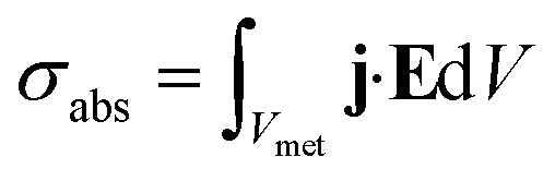 | (1) |
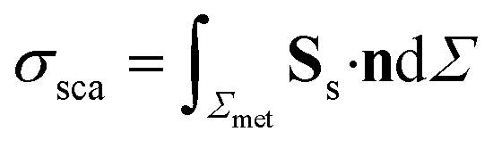 | (2) |
The extinction cross-section σext of one nanodisk is given by the sum of σabs and σsca:
| σext = σabs + σsca | (3) |
The absorbance A at the normal incidence of a sample with a surface density cs of identical, non-interacting nanodisks, each with extinction cross-section σext, is given by Lambert–Beer's law:
| A = csσext | (4) |
2.3 Sensitivity calculations
For wavelength-interrogated sensors, as for the systems under investigation, the response of the sensor is given by the spectral shift of the maximum of absorbance, λmax, due to the addition of an analyte: Δλ ≡ λ(ana)max − λ(0)max, where λ(0)max is the spectral position of the sensor maximum absorbance without the analyte and nmed = n(0)med = 1. The bulk sensitivity is then obtained by normalizing the spectral shift by the difference in the refractive index nmed of the medium around the sensor (i.e., the nanodisk), with or without the analyte, Δn = n(ana)med − n(0)med: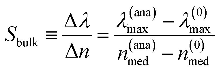 | (5) |
To define the local sensitivity, we consider the response of the sensors to a layer of analyte of thickness ta and refractive index na, according to the equation:11,24
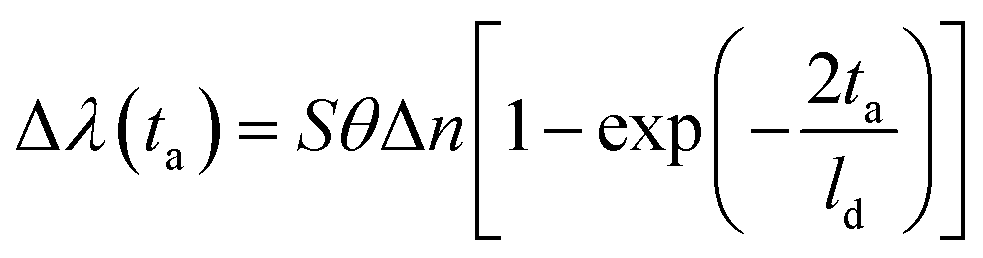 | (6) |
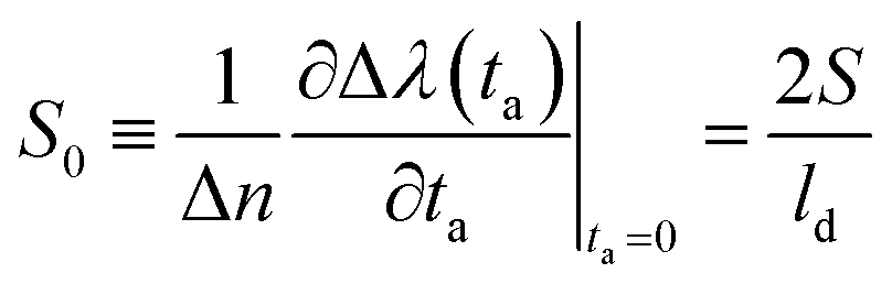 | (7) |
2.4 Experimental synthesis of disordered nanodisk arrays
Disordered nanodisk arrays (d-NDA) were fabricated by combining sparse colloidal lithography (SCL)28 and hole-mask lithography (HML).38 First, silica glass substrates were cleaned using an acid piranha solution (H2SO4![[thin space (1/6-em)]](https://www.rsc.org/images/entities/char_2009.gif) :H2O2, 3:1) at 90 °C for 1 h, followed by a basic piranha solution (NH3:H2O2, 3:1) at 80 °C for 15 minutes to enhance substrate hydrophilicity. Then, a 100 nm thick sacrificial layer of polymethylmethacrylate (PMMA, MW = 350000, from Sigma-Aldrich, in a 2.5% solution in toluene) was deposited by spin-coating on the SLG substrates, and cured on a hot plate at 80 °C for 10 minutes. A brief UV/ozone treatment was done to enhance PMMA hydrophilicity and then it was exposed to a 2% w/w poly(diallyldimethylammonium chloride) solution to obtain a positively charged surface. After this treatment, the substrates were exposed to a 0.2% w/w solution of COOH-terminated (negatively charged) polystyrene (PS) nanospheres with a nominal diameter of 300 nm (supplied by ThermoFisher) in order to obtain a sparse layer of nanoparticles adsorbed on the substrate surface. The PS nanospheres that were not adsorbed were washed away with Milli-Q water and the substrate was dried in nitrogen flux. A thin layer of Cr, about 20 nm thick, was deposited by magnetron sputtering and subsequently the PS nanoparticles were peeled off using adhesive tape, to obtain a nanohole mask. The PMMA layer was then selectively etched by reactive ion etching (RIE) in an Ar/O2 plasma down to the silica substrate. Finally, Au disordered nanodisk arrays were obtained by thermal evaporation of a 2 nm-thick layer of Cr as an adhesion layer followed by the evaporation of the Au layer, and the lift-off of the PMMA sacrificial layer by sonication in toluene. Scanning electron microscopy (SEM) images of the synthesized d-NDA were collected using a Zeiss Sigma HD field-emission SEM (FE-SEM), operated at 1 kV to reduce charging effects, using the InLens secondary electron detector. Atomic force microscopy (AFM) measurements were carried out using a NT-MDT Solver-Pro AFM in semi-contact mode.
:H2O2, 3:1) at 90 °C for 1 h, followed by a basic piranha solution (NH3:H2O2, 3:1) at 80 °C for 15 minutes to enhance substrate hydrophilicity. Then, a 100 nm thick sacrificial layer of polymethylmethacrylate (PMMA, MW = 350000, from Sigma-Aldrich, in a 2.5% solution in toluene) was deposited by spin-coating on the SLG substrates, and cured on a hot plate at 80 °C for 10 minutes. A brief UV/ozone treatment was done to enhance PMMA hydrophilicity and then it was exposed to a 2% w/w poly(diallyldimethylammonium chloride) solution to obtain a positively charged surface. After this treatment, the substrates were exposed to a 0.2% w/w solution of COOH-terminated (negatively charged) polystyrene (PS) nanospheres with a nominal diameter of 300 nm (supplied by ThermoFisher) in order to obtain a sparse layer of nanoparticles adsorbed on the substrate surface. The PS nanospheres that were not adsorbed were washed away with Milli-Q water and the substrate was dried in nitrogen flux. A thin layer of Cr, about 20 nm thick, was deposited by magnetron sputtering and subsequently the PS nanoparticles were peeled off using adhesive tape, to obtain a nanohole mask. The PMMA layer was then selectively etched by reactive ion etching (RIE) in an Ar/O2 plasma down to the silica substrate. Finally, Au disordered nanodisk arrays were obtained by thermal evaporation of a 2 nm-thick layer of Cr as an adhesion layer followed by the evaporation of the Au layer, and the lift-off of the PMMA sacrificial layer by sonication in toluene. Scanning electron microscopy (SEM) images of the synthesized d-NDA were collected using a Zeiss Sigma HD field-emission SEM (FE-SEM), operated at 1 kV to reduce charging effects, using the InLens secondary electron detector. Atomic force microscopy (AFM) measurements were carried out using a NT-MDT Solver-Pro AFM in semi-contact mode.
2.5 Sensitivity measurements
To determine the bulk sensitivity of the synthesized d-NDAs, the absorbance spectra of the samples were acquired in different media: air (nmed = 1), deionized water (nmed = 1.33) and ethanol (nmed = 1.36). The spectra were collected in the range 200–1100 nm using an OceanOptics HR4000 spectrophotometer with a OceanOptics DH2000 source. For the local sensitivity measurement, thin layers of SiO2 of increasing thickness (ta = (5.0 ± 0.2), (9.0 ± 0.2), (13.0 ± 0.2), and (21.0 ± 0.3) nm), measured by AFM were deposited by magnetron sputtering on the d-NDAs, and the absorbance spectra were acquired at each step. The refractive index of the silica layers was measured by spectroscopic ellipsometry with a J. Woolham V-VASE spectroscopic ellipsometer and it resulted in na = 1.40; the measured value is slightly lower than the tabulated one for silica, probably due to an imperfect stoichiometry/densification of the thin films obtained by magnetron sputtering.3 Results and discussion
To carry out the parametric optimization of the bulk and local sensitivities of the designed sensors, we varied the diameter D of the nanodisks in the range 100–400 nm and the height h in the range 50–110 nm. Random arrays of nanodisks characterized by any combination of these parameters can be fabricated by hole mask lithography.The first obtained result is the spectral position of the LSPR resonance of the nanodisk array, without the analyte (i.e., nmed = 1 and ta = 0), for each (D, h) combination considered. Fig. 2a shows the simulated extinction cross-section of six nanodisk arrays, with h = 70 nm and a different diameter D. In all the cases, the spectra have a well-defined resonance, and the spectral position of its maximum, λ(0)max, results strongly dependent on the nanodisk dimensions. To better visualize the dependence of λ(0)max on D and h, a contour plot is reported in Fig. 2b. As highlighted by the color scale, the variation of λ(0)max is quite large, ranging from about 520 nm to about 1280 nm. We note that this range is larger than the one obtained in similar parametric studies previously carried out on nanoprism arrays and reported in ref. 24. In that case, the resonance ranged between 600 nm and 1100 nm, even though the variation of parameters was larger than the present one. The capability to tune the spectral position of the resonance is extremely advantageous for biosensing applications, since it allows to optimally couple the sensor to a large set of experimental equipment (sources, detectors, etc.) and/or analyte features, to enhance the sensor sensitivity.24,53,54 As an example, in Fig. 2b we indicate the emission lines of some of the most common laser sources – Nd:YAG laser (fundamental, 1064 nm, and second harmonic, 532 nm), HeNe laser (633 nm) and Ti:Sapphire laser (tunable between 650 nm and 1100 nm, with the best efficiency around 800 nm) – showing that such a wide range of laser wavelengths can be used to excite resonantly the LSPR, e.g. for SERS sensing. Fig. 2b also clearly shows that the dependence on the disk diameter D is much more important than that on the height h, at least for normal incidence. Such a strong dependence on D is due to the nature of the plasmonic mode excited by the incident plane wave of modulus E0. Fig. 3a shows the distribution of local field enhancement (|FE| = |E|/E0) around a h = 70 nm, D = 250 nm nanodisk at z = 2 nm (i.e., at the interface between the nanodisk and the adhesion layer). Two lobes appear in the direction of the polarization of the incident wave. Fig. 3b shows the field enhancement distribution in the incidence plane (y = 0): in this case, the field enhancement is distributed along the full height of the nanodisk (the |FE| = 3 contour encircles the whole side of the nanodisk) with the two hottest spots at the top and at the bottom; even at the hottest spots, however, the field enhancement is never greater than 20. Fig. 3c shows the distribution of the electric field component in the incidence plane Ex: the amplitude is constant throughout the height of the nanodisk, confirming that the resonance can be labeled as dipolar.51 For spherical nanoparticles, Mie theory foresees a spectral shift of the LSPR towards longer wavelengths as the radius of the sphere is increased: this behavior is also found for the investigated nanodisk arrays.
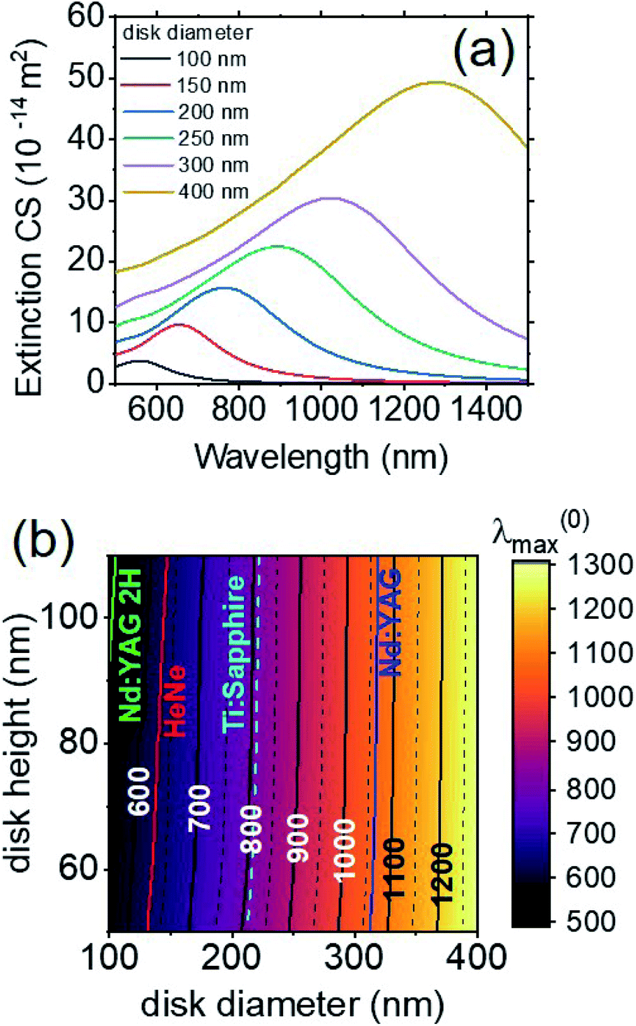 | ||
| Fig. 2 LSPR of the nanodisk array sensors, without the analyte (nmed = 1 and ta = 0). (a) Extinction cross-sections of nanodisks with height h = 70 nm and diameter D ranging from 100 nm to 400 nm. (b) Colored contour plot of the LSPR maximum wavelength, λ(0)max, as a function of D (horizontal axis) and h (vertical axis). The green, red, cyan and blue contour lines indicate, respectively, the wavelengths of the emission lines of some of the most common lasers: Nd:YAG second harmonic (532 nm), HeNe (633 nm), Ti:Sapphire (tunable between 650 nm and 1100 nm, with best efficiency around 800 nm) and Nd:YAG fundamental (1064 nm). | ||
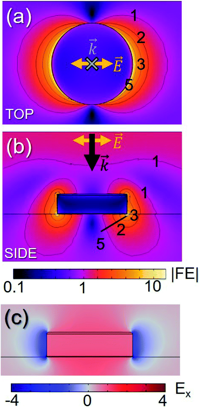 | ||
Fig. 3 Local field enhancement maps around a h = 70 nm, D = 250 nm nanodisk at λ(0)max = 894 nm, excited by a plane-wave traveling towards the negative ẑ direction and polarized along the ![[x with combining circumflex]](https://www.rsc.org/images/entities/i_char_0078_0302.gif) axis. (a) Top view at z = 2 nm and (b) side view in the y = 0 plane; black lines indicate the levels of field enhancement 1, 2, 3 and 5. (c) Side view of the distribution of the electric field component parallel to the polarization of the incident wave, Ex. axis. (a) Top view at z = 2 nm and (b) side view in the y = 0 plane; black lines indicate the levels of field enhancement 1, 2, 3 and 5. (c) Side view of the distribution of the electric field component parallel to the polarization of the incident wave, Ex. | ||
3.1 Local sensitivity optimization
To determine the local sensitivity of each (D, h) nanodisk configuration, first we computed the LSPR peak wavelength λ(ta) for different thicknesses of the analyte layer (ta = 2, 3, 5, and 10 nm) and we calculated the corresponding shifts Δλ(ta) with respect to the condition without the analyte. Then, the values of Δλ(ta) were fitted with an exponential function according to eqn (6), to obtain the limit sensitivity S and the effective near-field decay length ld. We recall that the surface coverage is considered to be θ = 1, and for the simulations the refractive index difference is set at Δn = 0.5. The local sensitivity is then calculated as S0 = 2S/ld (see eqn (7)). Fig. 4a shows the contour plot of S0 as a function of the nanodisk diameter D and height h. The highest local sensitivity is reached for D = 250 nm, h = 70 nm nanodisks and results in S(max)0 = 11.9 RIU−1, indicated with a star in Fig. 4a. An important issue in finding the maximum is the extension of its stability basin, which prevents large fluctuations in the sensors due to nanofabrication imperfections. The contour plot also shows that for a quite large region (patterned with vertical lines in the figure), approximately in the range 200 ≤ D ≤ 250 nm, and 55 ≤ h ≤ 80 nm, S0 is higher than 11.5 RIU−1, and that for an even larger region (patterned with horizontal lines) the sensitivity is still better than 11.0 RIU−1. We stress the fact that for sensors based on arrays of nanostructures, the difference in sensitivity among the nanostructures is important as much as the sensitivity itself; if the nanostructures had different sensitivities, as a consequence, for example, of the presence of defects or fabrication tolerances, the resulting LSPR shift would be the convolution of all the different shifts produced in the different populations, giving rise to a broadening of the measured spectra and thus to larger measurement errors. In the present case, for the investigated nanodisk arrays the wide region around the best performing parameter combination – for which S0 > 11.5 RIU−1 – assures that the broadening of the resonance due to small defects or imperfections has a low impact on the operation of the sensor; the designed sensors have a high stability with respect to fabrication tolerances, which makes them compatible with low-cost fabrication methods.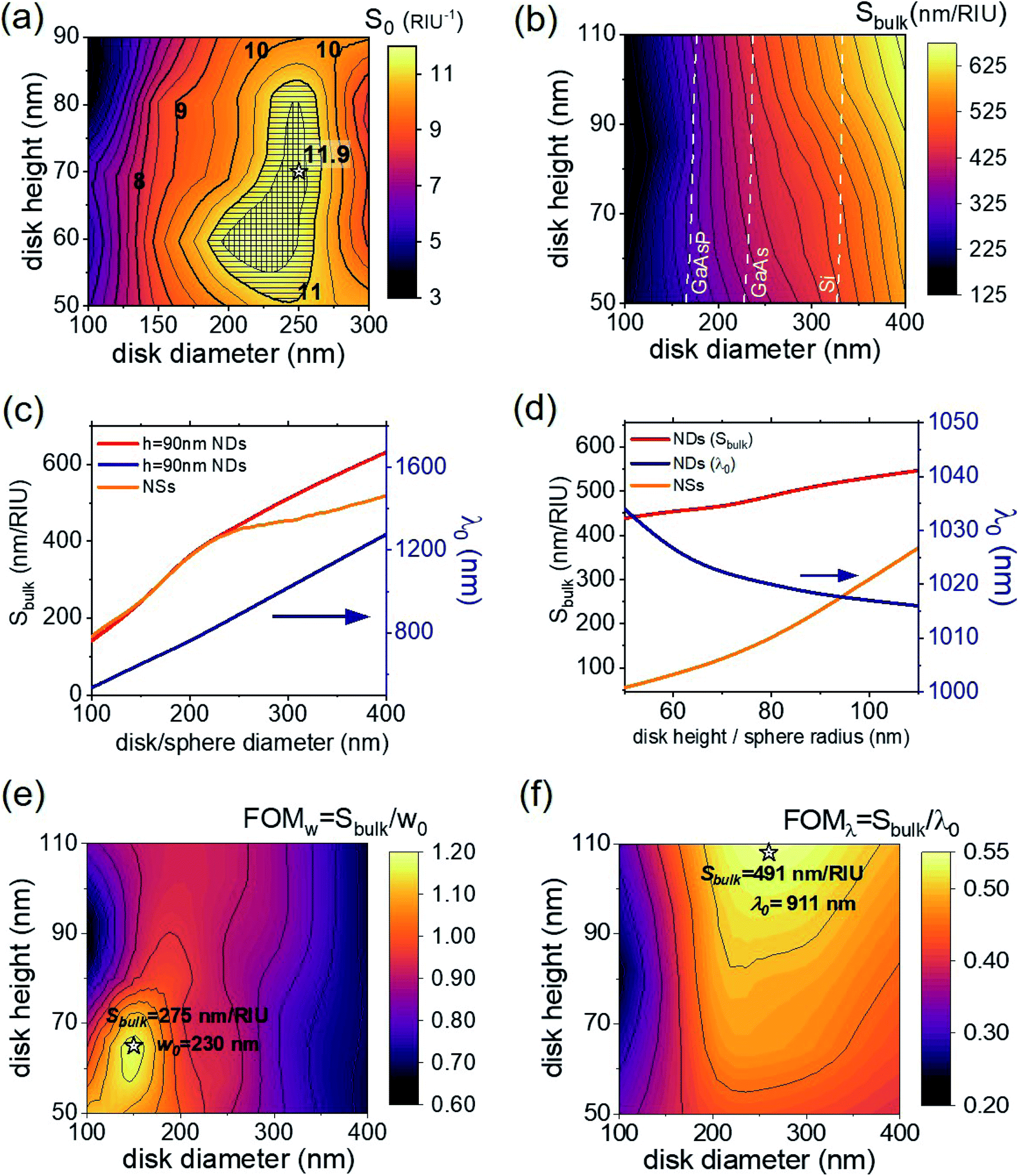 | ||
| Fig. 4 (a) Contour plot of the local sensitivity S0 as a function of the ND diameter D and height h. The star located at D = 250 nm, h = 70 nm indicates the best performing nanodisk configuration in terms of local sensitivity, with a value of S(max)0 = 11.9 RIU−1. The area patterned with vertical lines indicates the region where S0 > 11.5 RIU−1, while the one patterned with horizontal lines indicates the region where S0 > 11.0 RIU−1. (b) Contour plot of the bulk sensitivity Sbulk as a function of the nanodisk diameter D and height h. Yellow, green and blue dashed lines indicate the contour lines of nanodisks with λ(0)max equal to the upper limit of the working range of GaAsP, GaAs and Si detectors, respectively. (c) Left-hand scale: bulk sensitivity Sbulk of h = 90 nm nanodisks (red line) and isolated nanospheres (orange line) as a function of the diameter D; the nanosphere sensitivity has been normalized to the exposed surface of a nanodisk with the same diameter and height h = 90 nm. Right-hand scale, blue line: LSPR peak wavelength of h = 90 nm nanodisks as a function of the diameter D. (d) Left-hand scale: bulk sensitivity Sbulk of D = 300 nm nanodisks as a function of the height h (red line) and of isolated nanospheres as a function of the radius (orange line); the nanosphere sensitivity has been normalized to the exposed surface of a nanodisk with diameter D = 300 nm and height h. Right-hand scale (blue line): LSPR peak wavelength of D = 300 nm nanodisks as a function of the height h. (e) Contour plot of the figure of merit FOMw. (f) Contour plot of the figure of merit FOMλ. | ||
3.2 Bulk sensitivity optimization
To evaluate the bulk sensitivity of each (D, h) nanodisk configuration, we performed different simulations changing the refractive index of the environment surrounding the nanodisk from n(0)med = 1 to n(ana)med = 1.47. Then, the LSPR maximum wavelength λ(ana)max and the spectral shift Δλ = λ(ana)max − λ(0)max were calculated. The bulk sensitivity was obtained by applying eqn (5).Fig. 4b shows the bulk sensitivity as a function of the diameter of the nanodisk D (horizontal axis) and of the height h (vertical axis). In the investigated range, Sbulk does not show any local maximum; it grows with the increase of the diameter D and, with a less pronounced dependence, with the increase of the height h; for D = 400 nm and h = 110 nm the NDs reach a bulk sensitivity of S(max)bulk = 662 nm/RIU. As previously noted (Fig. 3c), the LSPR mode has a dipolar character, as for an isolated plasmonic nanosphere. In terms of bulk sensitivity, this parallel is evident. Fig. 4c shows the dependence of Sbulk on D for nanodisks with h = 90 nm (red line) and for nanospheres (orange line). For the nanospheres, the Mie sphere and coated sphere models are solved using an in-house implementation of Bohren's routines55 for MATLAB. In this case, to have a more meaningful comparison, the sensitivity was normalized to the exposed surface of a nanodisk with the same diameter and height h = 90 nm. Both curves show a slight upward concavity for diameters below about 250 nm; in this region the dependence of Sbulk on D is a super-linear function. Above this region, both curves show a linear dependence, with a slope of 1.26 ± 0.07 RIU−1 for the nanodisks (for the NSs the slope is about half that for the nanodisks: 0.58 ± 0.01 RIU−1). A similar dependence on the diameter is observed for nanodisks of different heights. Fig. 4d shows the trend of the bulk sensitivity as a function of the disk height (red line) for nanodisks with diameter D = 300 nm. Sbulk grows with the height as it does with the diameter. For comparison, the orange curve in Fig. 4d represents the bulk sensitivity of isolated nanospheres, as a function of the nanosphere radius, normalized, with the same approach described above, to the exposed surface of nanodisks of diameter D = 300 nm and height h. The blue curves in Fig. 4c and d (right-hand scale) show the trend of the LSPR peak wavelength as a function of D (for nanodisks with h = 90 nm, Fig. 4c) and as a function of h (for nanodisks with D = 200 nm, Fig. 4d). An almost linear dependence of λ(0)max on the diameter D is observed (Fig. 4c). On the contrary, the LSPR peak wavelength slightly blue-shifts when the height increases; however, the variation is very small, around 20 nm, in the explored range. Looking at the trend of bulk sensitivity and LSPR peak wavelength as a function of the nanodisk's diameter, it turns out that increasing D to get higher values of Sbulk also produces an increase of λ(0)max and λ(ana)max. As a consequence, the working spectral range of the sensor shifts towards the infrared region (for nanodisks with D = 400 nm λ(0)max is over 1250 nm for all the heights h); in this spectral region, the sensor may suffer from limitations due to light sources, detectors and optical components, and also the presence of characteristic absorption lines of solvents and media used for bulk sensing, such as water, ethanol or polymers. In this regard, as an example, the yellow, green and blue dashed lines in Fig. 4b indicate the contour lines of nanodisks with λ(0)max equal to the upper limit of the working range of three popular semiconductor detectors currently used in spectrophotometers and CCDs: GaAsP, GaAs and Si detectors, respectively; only nanodisks with geometric parameters lying on the left of these lines can be used with these detectors. It is worth saying that for bulk sensing the limits are even more strict, since the red-shifted resonance in the presence of the analyte layer should also lie in the working range of the selected detector.
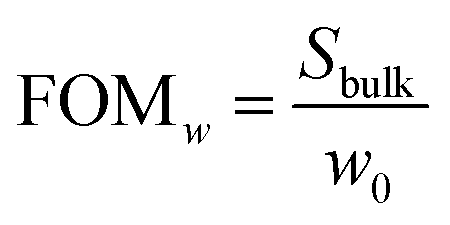
Furthermore, it is important to note that the full width at half maximum (FWHM) of the LSPR, w0, increases as the resonance red-shifts (see Fig. 2a); thus, larger nanodisks also yield broader resonances. To account also for this effect, we computed the following figure of merit (FOMw):
 | (8) |
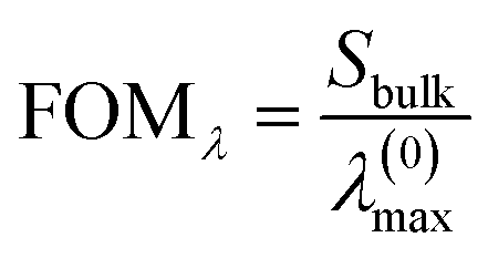
Fig. 4e shows a contour plot of FOMw as a function of nanodisks diameter and height. The highest value of FOMw = 1.2 RIU−1 is found for nanodisks with D = 150 nm and h = 65 nm, for which the bulk sensitivity is  , λ(0)max = 656 nm and w0 = 230 nm. FOMw is best suited for assessing better accuracy in the LSPR shift at low analyte concentration, i.e., to improve the limit of detection (LOD). On the other hand, for the situations in which it is more important to limit the LSPR wavelengths than the width of the resonance, a second figure of merit (FOMλ) can be considered, given by:
 | (9) |
Fig. 4f shows a contour plot of FOMλversus D and h. In this case, the maximum value of FOMλ = 0.54 RIU−1 is obtained for nanodisks with D = 260 nm and h = 110 nm, for which the bulk sensitivity  , λ(0)max = 911 nm and w0 = 466 nm, for which a value of FOMw = 1.05 RIU−1 is obtained.
As a final comment, it is worth saying that for biosensors aimed at detecting small molecules, the most significant benchmark figure to consider is the local sensitivity, S0, since typically in these nanosensors the analyte is immobilized within a few nm from the surface of the nanoparticles.24 On the other hand, when considering gas or chemical sensors, the bulk sensitivity, Sbulk, is a more interesting figure, as usually the sensors must probe very small variations in the refractive index of the medium in which they are embedded.16 In any case, hybrid configurations in which the gas analyte is entrapped for instance in a polymeric membrane at the nanoparticle surface take advantage of the enhanced local sensitivity.56
3.3 Bulk and local sensitivity of experimental d-NDA
Disordered nanodisk arrays (d-NDA) were synthesized by combining sparse colloidal lithography and hollow mask lithography (see Materials and methods). On the basis of the simulation results of the local sensitivity optimization (Fig. 4a), the nanodisks parameters were chosen to work close to the maximum of local sensitivity, S0. For the fabricated samples we obtained: D = 250 ± 20 nm and h = 70 ± 3 nm. A SEM image of the corresponding d-NDAs is presented in Fig. 5a. Fig. 5b shows the radial distribution function (RDF, g(r)) of the d-NDA calculated on 7416 nanodisks: an average distance (center-to-center) of ravg ≈ 590 nm is obtained. This means that the average surface-to-surface minimum distance between the nanodisks is dss = ravg − D ≈ 340 nm. From the FEM simulations we found that the field decay length in the array plane is ld = 18.8 ± 0.7 nm. Since dss ≫ ld, the nanodisks in the synthesized samples can be considered as non-interacting.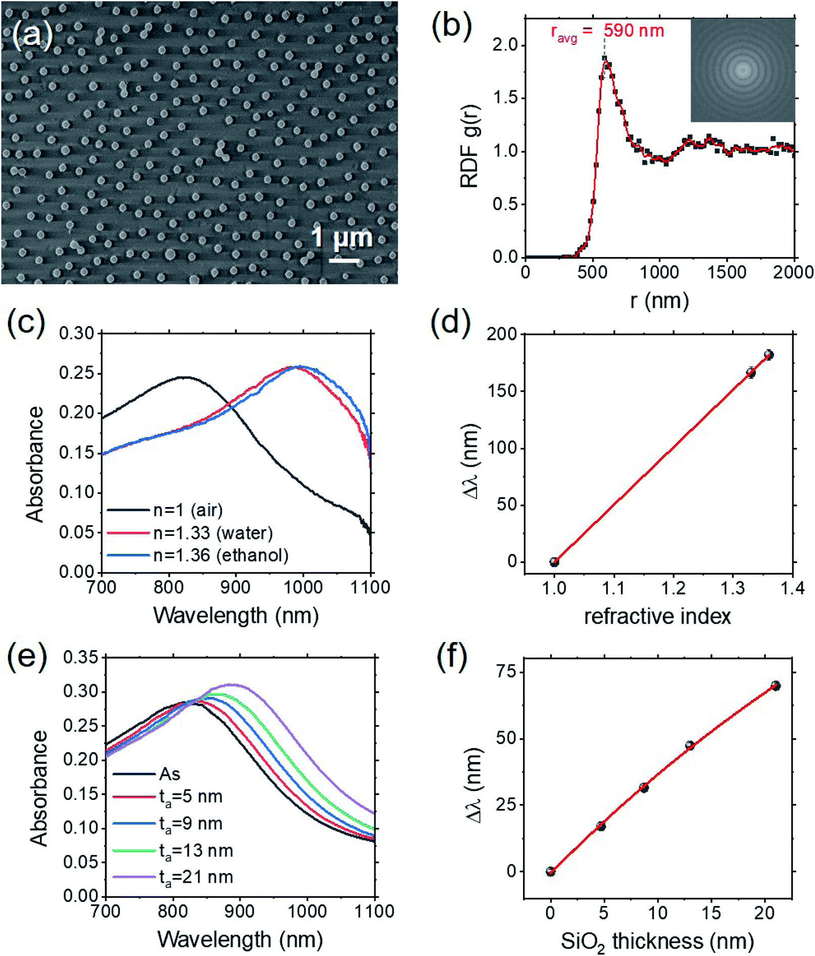 | ||
| Fig. 5 (a) SEM image of the fabricated d-NDA. (b) Radial density function g(r) computed on 7416 nanodisks. In the inset, the FFT of the original image is reported. (c) Absorbance spectra of the d-NDA in air (n = 1, gray), water (n = 1.33, red) and ethanol (n = 1.36, blue). (d) Δλ as a function of the refractive index nmed (gray dots); the red line is the linear fit of the data. (e) Absorbance spectra of the d-NDA covered by incremental layers of silica. (f) Δλ as a function of the thickness of the silica layer ta (gray dots); the red line is the nonlinear fit of the data using the exponential function in eqn (6). | ||
Fig. 5c shows the absorbance spectra of the d-NDA measured in air (nmed = 1), water (nmed = 1.33) and ethanol (nmed = 1.36). A progressive red-shift of the resonance maximum is obtained by increasing the refractive index of the medium, with respect to air (Δλ = 166 ± 2 nm for water and Δλ = 182 ± 2 nm for ethanol). As shown in Fig. 5d, the trend is linear, and the bulk sensitivity of the d-NDA can be computed from the slope of the line that fits the data, consistent with eqn (5). In the present case, we got S(exp)bulk = 505 ± 20 nm/RIU, even higher than the simulated one (Sbulk = 428 nm/RIU, Fig. 4b). This could be related to a possibly reduced effective thickness of the Cr adhesion layer which reduces the losses.
To determine the local sensitivity of the synthesized d-NDAs, a silica layer of increasing thickness was deposited on the samples by magnetron sputtering. Fig. 5e shows the absorbance spectra of the d-NDA after the deposition of the silica layer. Fig. 5f shows the corresponding redshifts Δλ, as a function of the layer thickness ta. The red line is the best-fitting curve obtained using eqn (6). The local sensitivity is then computed from the fitted values with eqn (7); the change of refractive index with respect to air is Δn = 0.40 (see Materials and methods). The resulting local sensitivity is S(exp)0 = 10.9 ± 1.0 RIU−1. This value is in very good agreement with the simulations (S(max)0 = 11.9 RIU−1), taking into account the presence of defects in the fabricated samples also.
These results confirm that the optimizations carried out for non-interacting nanodisks with FEM simulations can be successfully applied to disordered nanodisk arrays that can be experimentally realized with cost-effective methods.
To compare the performances of nanospheres and nanodisks, we considered nanospheres with the same diameter D as the nanodisks. In terms of local sensitivity, the best-performing nanodisks are the ones with D = 250 nm, h = 70 nm, for which the local sensitivity resulted in S(max)0 = 11.9 RIU−1. For an isolated nanosphere with D = 250 nm instead, we determined with the Mie model a local sensitivity of S(NS)0 = 10.1 RIU−1, about 20% less than that of the nanodisks. Moreover, we point out that while in the case of the nanospheres the analyte is all around the nanosphere, for the nanodisks the presence of the substrate limits the surface available for the analyte; nonetheless, the nanodisks perform better than nanospheres with the same diameter. Regarding the bulk sensitivity, as shown in Fig. 4c (red and orange lines), for nanospheres S(NS)bulk(D) is lower than the one computed for nanodisks, S(ND)bulk(D), for diameters D larger than 250 nm and nearly equal to it for D < 250 nm. Moreover, our results on bulk sensitivity can be compared to other literature data on isolated nanoparticles with different shapes57 or on spheres with increasing diameter.58 Our nanodisks optimized for the FOMw have a bulk sensitivity of 275 nm/RIU and a FOMw = 1.2. They outperform the nanospheres (FOMw = 0.6) and nanoparticles with a more exotic shape like nanobranches (FOMw = 0.8), which exhibit the largest bulk sensitivity (703 nm/RIU) among the different nanoshapes investigated in ref. 57. In any case, we would like to underline that the main aim of the present work is to optimize the sensing performances of random nanodisk arrays, more than finding the most sensitive nanostructure.
Concerning the nanoprism arrays, we performed, as described in ref. 24, a similar sensitivity optimization study for NPAs, making it possible to compare the best performing configurations of the two nanoarchitectures. For bulk sensing, we demonstrated that the best performing Au nanoprism arrays are NPAs with a0 = 700 nm, h = 140 nm, and L = 210 nm, which have a bulk sensitivity of S(max,NPA)bulk = 342 nm/RIU. Nanodisks overcome this value when D > 200 nm (see Fig. 4c, red curve). On the other hand, in terms of local sensitivity the maximum value obtained for the nanodisks is S(max)0 = 11.9 RIU−1 (Fig. 4a), which is sensibly lower than the value determined for the optimized NPAs, namely S(max,NPA)0 = 39 RIU−1 for a0 = 200 nm, h = 10 nm, and L = 60 nm Au NPAs.24 Nonetheless, in the case of nanodisks, the field distribution gives them two important advantages with respect to NPAs. The first advantage is that the presence of an adhesion layer negligibly affects the absorbance spectrum. As an example, Fig. 6a shows the effect of a 2 nm-thick Cr adhesion layer on the extinction cross-section of Au nanodisks; the resonance is almost unaffected by the presence of the adhesion layer and a negligible redshift and increase of the maximum occur when Cr is present. The presence of an adhesion layer instead has a dramatic effect on the nanoprism arrays. Fig. 6b shows a comparison between the extinction cross-section of a local sensitivity-optimized Au NPA, with (gray) and without (orange) the same 2 nm-thick Cr adhesion layer. In this case, the resonance almost vanishes when Cr is present. Thus, the best performing NPAs must be reconsidered if an adhesion layer has to be added to the nanostructure.
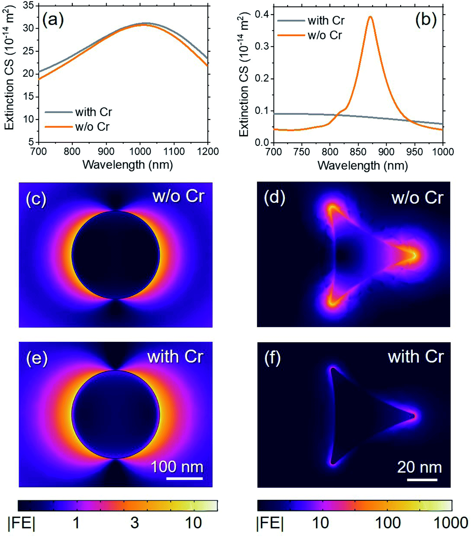 | ||
| Fig. 6 Simulated extinction cross-section spectra of Au nanodisks (a) and local sensitivity-optimized Au nanoprism array (b) with (gray curves) and without (orange curves) a 2 nm-thick Cr adhesion layer. (c–f) Maps of local field enhancement close to the surface of a nanodisk (left column) and of a nanoprism (right column) without (c and d) and with (e and f) the adhesion layer of Cr. | ||
The differences in the behavior of nanodisks and nanoprisms is due to the field localization and enhancement given by the two geometries. The smooth side surface of the nanodisks produces a field enhancement lower than 20, but is homogeneously distributed along almost all the surface itself, as shown in Fig. 6c. Conversely, Fig. 6d shows that the field enhancement around the nanoprisms is strongly confined at the nanoprism tips, where it can reach a value larger than 1000. Losses due to Joule's heating are present at each point of the nanostructure, with a local power dissipation given by the product ε2|E|2, where ε2 is the imaginary part of the dielectric function of the material. ε2 is more than one order of magnitude higher for Cr than for Au; thus, in the presence of a strong local field the losses in the Cr layer are larger than the losses in the plasmonic metal. In the case of nanodisks, Fig. 6e shows that the field enhancement is never as high as it is needed to produce significant losses in the adhesion layer; the maximum field enhancement is reduced by a negligible factor by the presence of Cr and only a slight stretching of the field decay length in the surrounding medium is observed. Conversely, in the case of nanoprisms the field is so strong at the tips that the losses due to Cr damp the energy stored in the LSPR, giving rise to a low Q-factor resonance, and reducing the field enhancement by a factor of more than 25 (Fig. 6f). We further stress that the fact that the losses in the adhesion layer are so large that the plasmonic resonance is almost totally quenched represents a major limitation of the NPA architecture; since the exposure to analytes usually implies functionalization in solution and subsequent wash, rinse and dry cycles, the option of using an adhesion layer strongly enhance the stability of the sensors during the whole process.
The second advantage of nanodisks with respect to the nanoprism configuration is that, since in the case of nanodisks the mode is spread around the nanostructure (Fig. 3, 6c and e), the sensitivity to small molecules is less dependent on the precise binding position of the molecule relative to the nanodisk's surface. This implies that a lower concentration of molecules is sufficient to assure that the number of molecules needed to get a detectable signal are in the region where the mode is strong.
4 Conclusions
The bulk and local sensitivities of non-interacting Au nanodisk arrays have been investigated by finite elements method electrodynamic simulations. The diameter D and height h of the nanodisks are varied in the range 100 ≤ D ≤ 400 nm and 50 ≤ h ≤ 110 nm, to determine the optimal configurations to be used for sensing. The highest local sensitivity, S(max)0 = 11.9 RIU−1, is obtained for nanodisks with D = 250 nm and h = 70 nm. We also found the region where S0 > 11.5 RIU−1 (i.e., within 3.3% below the maximum value) extends to a quite large range of (D, h) combinations. Regarding the bulk sensitivity, we observed that no local maximum exists for the explored nanodisks, whose resonance is within the vis-NIR range, and that larger nanodisk diameters and, to a less extent, larger heights produce better bulk sensitivities. For the extreme point considered (D = 400 nm and h = 110 nm) we got a maximum bulk sensitivity S(max)bulk = 662 nm/RIU. Moreover, two figures of merit (FOMλ and FOMw) have been introduced to account for the progressive red-shift of the resonance as the diameter of the nanodisks is increased and correspondingly, its width is increased. The simulated results have been compared with those obtained experimentally with disordered, non-interacting nanodisk arrays synthesized by combining sparse colloidal lithography and hollow mask lithography. The samples were fabricated choosing the parameter combination that gave us the highest local sensitivity in the simulations. A very good agreement between the experimental and simulated results was obtained, confirming that the optimization performed with the simulations is directly applicable to nanosensors realized with cost-effective methods, due to the quite large stability basin around the maximum sensitivities. Therefore, the nanodisks were revealed to be extremely robust against fabrication defects. Finally, the performances of the investigated non-interacting nanodisk arrays have been compared with those of two other, widely investigated, geometries: nanospheres and nanoprism arrays. The results show that for all the configurations explored, the nanodisks perform better than nanospheres with the same diameter, both in terms of bulk and local sensitivity. Regarding the comparison with nanoprism arrays, instead, the simulations demonstrated that a higher bulk sensitivity can be obtained with nanodisks with respect to the best performing nanoprism arrays, whereas these last have a much larger local sensitivity, about 4 times larger, than the optimized nanodisks. Nonetheless, in the case of nanodisks, the local field distribution gives them two important advantages: the first is that the possible presence of an adhesion layer does not affect the operation of the sensor, contrary to what happens for nanoprism arrays, making nanodisk array sensors more suitable to be used with aggressive chemical agents, for which structurally stable nanostructures are necessary. The second advantage is the possibility to work with lower concentrations of analyte molecules which makes these systems particularly useful for all the situations in which the availability of analyte molecules is limited.Conflicts of interest
There are no conflicts to declare.Acknowledgements
This work has been partially supported by the University of Padova with the Project BINDER (CPDA153538) and by the Physics and Astronomy Department of the University of Padova with the Project BIRD183751.References
- J. A. Schuller, E. S. Barnard, W. Cai, Y. C. Jun, J. S. White and M. L. Brongersma, Nat. Mater., 2010, 9, 193–204 CrossRef CAS PubMed.
- T. Cesca, E. V. García-Ramírez, H. Sánchez-Esquivel, N. Michieli, B. Kalinic, J. M. Gómez-Cervantes, R. Rangel-Rojo, J. A. Reyes-Esqueda and G. Mattei, RSC Adv., 2017, 7, 17741–17747 RSC.
- H. Sánchez-Esquivel, K. Y. Raygoza-Sánchez, R. Rangel-Rojo, E. Gemo, N. Michieli, B. Kalinic, J. A. Reyes-Esqueda, T. Cesca and G. Mattei, Sci. Rep., 2017, 7, 5307 CrossRef PubMed.
- H. Sánchez-Esquivel, K. Y. Raygoza-Sanchez, R. Rangel-Rojo, B. Kalinic, N. Michieli, T. Cesca and G. Mattei, Nanoscale, 2018, 10, 5182–5190 RSC.
- J. N. Munday and H. A. Atwater, Nano Lett., 2010, 11, 2195–2201 CrossRef PubMed.
- V. E. Ferry, M. A. Verschuuren, H. B. Li, E. Verhagen, R. J. Walters, R. E. Schropp, H. A. Atwater and A. Polman, Opt. Express, 2010, 18, A237–A245 CrossRef CAS PubMed.
- Y.-S. No, J.-H. Choi, H.-S. Ee, M.-S. Hwang, K.-Y. Jeong, E.-K. Lee, M.-K. Seo, S.-H. Kwon and H.-G. Park, Nano Lett., 2013, 13, 772–776 CrossRef CAS PubMed.
- N. Michieli, B. Kalinic, C. Scian, T. Cesca and G. Mattei, ACS Photonics, 2018, 5, 2189–2199 CrossRef CAS.
- B. Kalinic, T. Cesca, C. Scian, N. Michieli, I. G. Balasa, E. Trave and G. Mattei, Phys. Status Solidi A, 2017, 1700437, 1700437 Search PubMed.
- T. Cesca, N. Michieli, B. Kalinic, I. G. Balasa, R. Rangel-Rojo, J. A. Reyes-Esqueda and G. Mattei, Mater. Sci. Semicond. Process., 2019, 92, 2–9 CrossRef CAS.
- J. N. Anker, W. P. Hall, O. Lyandres, N. C. Shah, J. Zhao and R. P. Van Duyne, Nat. Mater., 2008, 7, 442–453 CrossRef CAS PubMed.
- M. E. Stewart, C. R. Anderton, L. B. Thompson, J. Maria, S. K. Gray, J. A. Rogers and R. G. Nuzzo, Chem. Rev., 2008, 108, 494–521 CrossRef CAS PubMed.
- A. G. Brolo, Nat. Photonics, 2012, 6, 709–713 CrossRef CAS.
- O. Limaj, D. Etezadi, N. J. Wittenberg, D. Rodrigo, D. Yoo, S.-H. Oh and H. Altug, Nano Lett., 2016, 16, 1502–1508 CrossRef CAS PubMed.
- V. Russo, N. T. Michieli, T. Cesca, C. Scian, D. Silvestri, M. Morpurgo and G. Mattei, Nanoscale, 2017, 9, 10117–10125 RSC.
- L. Brigo, N. Michieli, L. Artiglia, C. Scian, G. A. Rizzi, G. Granozzi, G. Mattei, A. Martucci and G. Brusatin, ACS Appl. Mater. Interfaces, 2014, 6, 7773–7781 CrossRef CAS PubMed.
- M. Sturaro, E. Della Gaspera, N. Michieli, C. Cantalini, S. M. Emamjomeh, M. Guglielmi and A. Martucci, ACS Appl. Mater. Interfaces, 2016, 8, 30440–30448 CrossRef CAS PubMed.
- T. H. Joo, M. S. Kim and K. Kim, J. Raman Spectrosc., 1987, 18, 57–60 CrossRef CAS.
- J. Kneipp, H. Kneipp and K. Kneipp, Chem. Soc. Rev., 2008, 37, 1052–1060 RSC.
- N. Michieli, R. Pilot, V. Russo, C. Scian, F. Todescato, R. Signorini, S. Agnoli, T. Cesca, R. Bozio and G. Mattei, RSC Adv., 2017, 7, 369–378 RSC.
- M. D. Malinsky, K. L. Kelly, G. C. Schatz and R. P. Van Duyne, J. Am. Chem. Soc., 2001, 123, 1471–1482 CrossRef CAS.
- J. J. Mock, D. R. Smith and S. Schultz, Nano Lett., 2003, 3, 485–491 CrossRef CAS.
- S. R. Beeram and F. P. Zamborini, J. Phys. Chem. C, 2011, 115, 7364–7371 CrossRef CAS.
- N. Michieli, B. Kalinic, C. Scian, T. Cesca and G. Mattei, Biosens. Bioelectron., 2015, 65, 346–353 CrossRef CAS PubMed.
- J. C. Hulteen, D. A. Treichel, M. T. Smith, M. L. Duval, T. R. Jensen and R. P. Van Duyne, J. Phys. Chem. B, 1999, 103, 3854–3863 CrossRef CAS.
- T. R. Jensen, M. D. Malinsky, C. L. Haynes and R. P. Van Duyne, J. Phys. Chem. B, 2000, 104, 10549–10556 CrossRef CAS.
- C. L. Haynes and R. P. Van Duyne, J. Phys. Chem. B, 2001, 105, 5599–5611 CrossRef CAS.
- P. Hanarp, D. S. Sutherland, J. Gold and B. Kasemo, Colloids Surf., A, 2003, 214, 23–36 CrossRef CAS.
- T. H. Reilly III, R. C. Tenent, T. M. Barnes, K. L. Rowlen and J. van de Lagemaat, ACS Nano, 2010, 4, 615–624 CrossRef PubMed.
- T. Cesca, N. Michieli, B. Kalinic, A. Sánchez-Espinoza, M. Rattin, V. Russo, V. Mattarello, C. Scian, P. Mazzoldi and G. Mattei, Nanoscale, 2015, 7, 12411–12418 RSC.
- J. W. Menezes, J. Ferreira, M. J. Santos, L. Cescato and A. G. Brolo, Adv. Funct. Mater., 2010, 20, 3918–3924 CrossRef CAS.
- H. Im, S. H. Lee, N. J. Wittenberg, T. W. Johnson, N. C. Lindquist, P. Nagpal, D. J. Norris and S.-H. Oh, ACS Nano, 2011, 5, 6244–6253 CrossRef CAS PubMed.
- Y. Wang, A. Kar, A. Paterson, K. Kourentzi, H. Le, P. Ruchhoeft, R. Willson and J. Bao, ACS Photonics, 2014, 1, 241–245 CrossRef CAS PubMed.
- Y.-C. Chang, H.-C. Chung, S.-C. Lu and T.-F. Guo, Nanotechnology, 2013, 24, 095302 CrossRef PubMed.
- P. K. Jain, W. Huang and M. A. El-Sayed, Nano Lett., 2007, 7, 2080–2088 CrossRef CAS.
- B. M. Reinhard, M. Siu, H. Agarwal, A. P. Alivisatos and J. Liphardt, Nano Lett., 2005, 5, 2246–2252 CrossRef CAS PubMed.
- H. Wang and B. M. Reinhard, J. Phys. Chem. C, 2009, 113, 11215–11222 CrossRef CAS PubMed.
- H. Fredriksson, Y. Alaverdyan, A. Dmitriev, C. Langhammer, D. S. Sutherland, M. Zäch and B. Kasemo, Adv. Mater., 2007, 19, 4297–4302 CrossRef CAS.
- S. Cataldo, J. Zhao, F. Neubrech, B. Frank, C. Zhang, P. V. Braun and H. Giessen, ACS Nano, 2011, 6, 979–985 CrossRef PubMed.
- B. D. Busbee, S. O. Obare and C. J. Murphy, Adv. Mater., 2003, 15, 414–416 CrossRef CAS.
- C. L. Nehl, H. W. Liao and J. H. Hafner, Nano Lett., 2006, 6, 683–688 CrossRef CAS PubMed.
- H. Chen, X. Kou, Z. Yang, W. Ni and J. Wang, Langmuir, 2008, 24, 5233–5237 CrossRef CAS PubMed.
- H. Chen, L. Shao, K. C. Woo, T. Ming, H.-Q. Lin and J. Wang, J. Phys. Chem. C, 2009, 113, 17691–17697 CrossRef CAS.
- J. Becker, A. Trugler, A. Jakab, U. Hohenester and C. Soennichsen, Plasmonics, 2010, 5, 161–167 CrossRef CAS.
- R. Bukasov, T. A. Ali, P. Nordlander and J. S. Shumaker-Parry, ACS Nano, 2010, 4, 6639–6650 CrossRef CAS PubMed.
- H. Wei, A. Reyes-Coronado, P. Nordlander, J. Aizpurua and H. Xu, ACS Nano, 2010, 4, 2649–2654 CrossRef CAS PubMed.
- L. S. Slaughter, W.-S. Chang, P. Swanglap, A. Tcherniak, B. P. Khanal, E. R. Zubarev and S. Link, J. Phys. Chem. C, 2010, 114, 4934–4938 CrossRef CAS.
- K. M. Mayer and J. H. Hafner, Chem. Rev., 2011, 111, 3828–3857 CrossRef CAS PubMed.
- G. K. Joshi, P. J. McClory, B. B. Muhoberac, A. Kumbhar, K. A. Smith and R. Sardar, J. Phys. Chem. C, 2012, 116, 20990–21000 CrossRef CAS.
- C. Sonnichsen and A. P. Alivisatos, Nano Lett., 2005, 5, 301–304 CrossRef PubMed.
- G. Mie, Ann. Phys., 1908, 330, 377–445 CrossRef.
- L. Brigo, G. Mattei, N. Michieli and G. Brusatin, Microelectron. Eng., 2012, 97, 193–196 CrossRef CAS.
- J. Zhao, L. Jensen, J. Sung, S. Zou, G. C. Schatz and R. P. Van Duyne, J. Am. Chem. Soc., 2007, 129, 7647–7656 CrossRef CAS PubMed.
- J. Zhao, A. Das, G. C. Schatz, S. G. Sligar and R. P. Van Duyne, J. Phys. Chem. C, 2008, 112, 13084–13088 CrossRef CAS.
- C. F. Bohren and D. R. Huffman, Absorption and Scattering of Light by Small Particles, John Wiley & Sons, 2008 Search PubMed.
- F. A. A. Nugroho, I. Darmadi, L. Cusinato, A. Susarrey-Arce, H. Schreuders, L. J. Bannenberg, A. B. d. S. Fanta, S. Kadkhodazadeh, J. B. Wagner, T. J. Antosiewicz, A. Hellman, V. P. Zhdanov, B. Dam and C. Langhammer, Nat. Mater., 2019, 18, 489–495 CrossRef CAS PubMed.
- H. Chen, X. Kou, Z. Yang, W. Ni and J. Wang, Langmuir, 2008, 24, 5233–5237 CrossRef CAS PubMed.
- N. Nath and A. Chilkoti, Anal. Chem., 2002, 74, 504–509 CrossRef CAS PubMed.
| This journal is © The Royal Society of Chemistry 2020 |