
 Open Access Article
 This Open Access Article is licensed under a Creative Commons Attribution-Non Commercial 3.0 Unported Licence
Interfacial nanoconnections and enhanced mechanistic studies of metallic coatings for molecular gluing on polymer surfaces†
Dexin
Chen
 *ad,
Zhixin
Kang
*b,
Hidetoshi
Hirahara
c and
Wei
Li
ad
*ad,
Zhixin
Kang
*b,
Hidetoshi
Hirahara
c and
Wei
Li
ad
aInstitute of Advanced Wear & Corrosion Resistant and Functional Materials, Jinan University, 601 Huangpu Avenue West, Guangzhou 510632, China. E-mail: dxchen@jnu.edu.cn
bGuangdong Key Laboratory for Advanced Metallic Materials Processing, School of Mechanical and Automotive Engineering, South China University of Technology, 381 Wushan, Guangzhou 510640, China. E-mail: zxkang@scut.edu.cn
cFaculty of Science and Engineering, Iwate University, 4-3-5 Ueda, Morioka 020-8551, Japan
dShaoguan Research Institute of Jinan University, Wujiang District, Shaoguan 512027, China
First published on 13th April 2020
Abstract
Interfacial adhesion has been identified as being key for realizing flexible devices. Here, strong interfacial nanoconnections involving metallic patterns on polymer surfaces were fabricated via a molecular bonding approach, which includes UV-assisted grafting and molecular self-assembly. The interfacial characteristics of conductive patterns on liquid crystal polymer substrates were observed via transmission electron microscopy and atomic force microscopy infrared spectroscopy. The interfacial molecular layers have a thickness of 10 nm. Due to the successful molecular bonding modifications, interfacial adhesion has been sufficiently improved; in particular, the peel-related breakage sites will be located in the modified layers on the plastic surface beneath the interface after the metallic coatings are peeled off. Integrating X-ray photoelectron spectroscopy, infrared spectroscopy, and scanning electron microscopy results, the molecular bonding mechanism has been revealed: UV-assisted grafting and self-assembly result in the construction of interfacial molecular architectures, which provide nanosized connecting bridges between the metallic patterns and polymer surfaces. Such in-depth interfacial studies can offer insight into interfacial adhesion, which will impact on the development of metal/polymer composite systems and continue to push the improvement of flexible devices.
1. Introduction
Flexible circuits for electronic devices, such as metallic coatings on plastic substrates, have recently attracted great attention due to the existence of several promising flexible device applications, such as printed circuit boards, biochips, supercapacitors, and sensors.1–8 These hybrid systems exhibit excellent integrability with high quality due to the use of polymer films, giving rise to the multi-interfacial adhesion of dissimilar materials.9,10 The interfacial interactions provide an important pathway for integrating the desired materials, which is one of the key steps for realizing multifunctional, lightweight and microminiaturized devices.11More recently, numerous surface modification techniques have been developed to improve the interfacial adhesion in flexible electronic systems,12–14 such as etching,10,15 physical interlocking,11,16–20 plasma activation,21,22 and molecular grafting.23–26 Among these, surface-the use of grafting polymer brushes, which are commonly based on surface-initiated polymerization methods, leads to an increase in the numbers of covalent bonds between circuits and substrates, which are stronger than electrostatic interactions, hydrogen bonds, and van der Waals forces.27 This advantage, together with high efficiency and simplicity, makes molecular grafting attractive for improving interfacial adhesion in flexible electronics. For example, the Zheng group12 prepared transparent and covalently bonded polymer coatings (namely PMETAC) on different substrates, enhancing the adhesion of printed multiscale, flexible, foldable, and stretchable metal conductors significantly. Kwon presented a nanostructured self-assembled silane monolayer, which has been introduced onto polymer surfaces to improve the interfacial adhesion of Cu patterns,28 resulting in a superior adhesion strength of 1192 N m−1 and mechanical flexibility over 100![[thin space (1/6-em)]](https://www.rsc.org/images/entities/char_2009.gif) 000 bending cycles. Polydopamine, a biomolecule with universal adhesion, has been used to prepare robust well-defined metal Ag or Cu patterns on PTFE plastics,29 demonstrating suitability for applications in flexible electronics. However, most studies have focused on the fabrication of flexible devices with enhanced interfacial adhesion via molecular grafting, and there are very few works that deeply study the details of the connections between dissimilar materials or mechanisms that could lead to adhesion improvements.
000 bending cycles. Polydopamine, a biomolecule with universal adhesion, has been used to prepare robust well-defined metal Ag or Cu patterns on PTFE plastics,29 demonstrating suitability for applications in flexible electronics. However, most studies have focused on the fabrication of flexible devices with enhanced interfacial adhesion via molecular grafting, and there are very few works that deeply study the details of the connections between dissimilar materials or mechanisms that could lead to adhesion improvements.
In this work, surface modification methods were used to construct molecular nanobonding between metallic coatings and polymer substrates, including corona, UV-assisted grafting and self-assembly techniques. The interfacial characteristics were observed via transmission electron microscopy (TEM) and atomic force microscopy infrared spectroscopy (AFM-IR) for the first time. 90° peel testing was used for interfacial adhesion quantitative analysis. After peeling, surface feathers from the liquid crystal polymer (LCP) and Cu sides were studied via scanning electron microscopy (SEM). In order to figure out the adhesion mechanism related to metal coatings onto LCP substrates, X-ray photoelectron spectroscopy (XPS), Fourier-transform infrared spectroscopy (FTIR), and SEM were used to detail the chemical composition, chemical state and surface morphology data from LCP surfaces after each modification process.
2. Experimental section
2.1. Liquid crystal polymer
Pristine Vectran LCP (molecular structure as shown in Fig. S1†) sheets were used as received from ALPS Electric Co., Ltd (Japan). The sheets were 1.5 mm thick, with a width of 4 cm and a length of 5 cm.2.2. Reagents
The special chemicals 6-(3-triethoxysilylpropylamino)-1,3,5-triazine-2,4-azide (pTES, molecular structure as shown in Fig. S2a†) and 6-(3-triethoxysilylpropylamino)-1,3,5-triazine-2,4-dithiol monosodium (nTES, molecular structure as shown in Fig. S2b†) were obtained from Sulfur Chemical Institute, Japan. Other reagents were purchased from commercial sources and used without further treatment.2.3. Surface modification of LCP
pTES/nTES solutions were produced by dissolving pTES/nTES molecules in absolute ethyl alcohol or distilled water at different concentrations (0.10–3.0 wt%). For UV-assisted pTES grafting, the cleaned LCP substrates were dipped into 2 mmol L−1 pTES alcoholic solution for 10 s at ambient temperature, allowed to dry, and then exposed to ultraviolet radiation (254 nm, 0.1 J cm−2). After that, the samples were ultrasonically cleaned with absolute ethyl alcohol for 1 min to remove inactivated pTES molecules. For corona activation, LCP was treated using Corona Master apparatus (Shinko Electric & Instrumentation Co., Ltd) for 3 min at ambient temperature. For nTES assembly, the activated samples were immediately immersed into nTES solution for various treatment times, followed by washing with plenty of distilled water.2.4. Metallization of modified LCP
Ag metal coatings were deposited layer-by-layer on the polymer surfaces, and in-depth structural characterization of the coatings was carried out as described in a previous paper.30 Samples were immersed in a sensitizing solution (0.1 mol L−1 SnCl2 and 40 mL L−1 HCl) for 5 min. Freshly prepared Ag salt (0.1 mol L−1 AgNO3 and 50 mL L−1 25% NH3·H2O) and reducing (1 mol L−1 glyoxal and 0.1 mmol L−1 triethanolamine) agents were sprayed onto the LCP samples in a glove box. Then, the substrates were thoroughly rinsed with distilled water and cured at 75 °C in an air oven for 10 min to finish the metallization process.2.5. Interfacial analysis
The Al plate and Ag coatings were treated with 0.1 mol L−1 nTES solution, and adhered to each other under 0.1 MPa pressure for 10 min. Then, the samples were cut using a focused ion beam (FIB) system (MI-4050, Hitachi High-Technologies Corporation) to produce TEM cross-section samples. The interfacial features of Ag/LCP were studied using transmission electron microscopy (TEM, JEM-2100, JEOL, Japan), with a scanning voltage of 200 kV. Energy dispersion spectroscopy (EDS) data were obtained using an EDAX detector attached to the JEM-2100 apparatus. The micro-interfacial morphologies and chemical compositions were studied using atomic force microscopy infrared spectroscopy (AFM-IR, nanoIR2, Anasys Instruments Corporation). The AFM-IR samples were prepared using a precision vertical diamond wire saw (Model 3242, Well Diamond Wire Saws, Inc.). The adhesion of Ag films on ABS was evaluated via a standard cross-cut test with polyimide tape. In addition, adhesive strength was quantified via the 90° peel test method using a multi-purpose bond tester (90 Degree Peel Tester, Imada Inc., Japan) at ambient temperature with a separation rate of 50 mm min−1.2.6. Surface characterization
The surface morphologies of the LCP surfaces were studied via scanning electron microscopy (SEM, VE-8800, Keyence Co.). Contact angle measurements (OCA35, Dataphysics) were used to measure the wettability of the modified LCP. X-ray photoelectron spectroscopy (XPS, PHI Quantera, ULVAC-PHI Inc., Japan) with an Al Kα X-ray source at a 45° take-off angle was used to study the elemental compositions of the LCP surfaces. Survey spectra were recorded at a constant analyzer pass energy of 280eV over a range from 0 to 1000eV. The intensities of specific elements were recorded at a constant analyzer pass energy of 69eV. The high-resolution data was corrected using the standard C 1s binding energy (284.6eV). The surface chemistry was also characterized via Fourier-transform infrared spectroscopy (FTIR, Thermo Nicolet NEXUS 670) via the diffuse reflection method.
3. Results and discussion
3.1. Interfacial morphology
Liquid crystal polymer (LCP) exhibits a high moisture absorption rate, high-frequency electrical loss, and low mechanical stability, and it has been widely used in electronic devices.31–35 In this work, LCP was used as a substrate for modification and metallization procedures. To study the interfaces of the samples obtained via UV-assisted pTES grafting and nTES assembly (shorted to p–nTES) in detail, Ag-coated LCP was adhered to an Al plate and observed via transmission electron microscopy (TEM); a schematic drawing of the set-up is shown in Fig. 1a. From the TEM image in Fig. 1b, the thickness of the LbL-deposited Ag coating is about 60 nm, and the Ag–LCP interface shows grey features, different from the Ag coating and LCP. As depicted in Fig. 1c, the grey layer has a thickness of 10 nm, meaning that the connecting area is on the nanoscale. From EDS studies (Fig. 1d and e), spectra from the Ag coating side show obvious Ag peaks, while Al and Si may come from the Al plate during sample preparation. According to the results of element analysis (Table S1†), the Ag coating (Point 1) is composed of C, O, Al, Si and Ag (86.02 wt%) elements. The interface shows identifiable N (8.40 wt%) and S (0.73 wt%) peaks, which are specific characteristics of nTES used for modifying the LCP surface, and less Ag (15.46 wt%). EDS analysis at Point 3, the LCP side, shows C (80.05 wt%) and O (16.20 wt%) elements from LCP. | ||
| Fig. 1 TEM results from the interface: (a) a schematic drawing of the set-up used for TEM analysis; (b) a TEM image and (c) zoomed-in image of the interface between the Ag coating and LCP; (d) EDS results from Point 1 of figure (c), the Ag side, (e) EDS results from Point 2, the interface, and (f) EDS results from Point 3, the LCP side. | ||
In this study, the interfaces of metallic coatings on LCP were characterized via atomic force microscope infrared spectroscopy (AFM-IR), as shown in Fig. 2. AFM-IR provides nanoscale vibrational spectroscopy by combining the spatial resolution of atomic force microscopy with the chemical analysis capabilities of infrared spectroscopy,36 as shown in Fig. 2a. From AFM imaging, as shown in Fig. 2b, there is a distinct chasm between the LbL deposited Ag and LCP substrate. The interface morphology shows lamellar feathers (Fig. 2b), which were a result of the diamond wire cutting process during sample preparation. IR spectra (Fig. 2c) from the left four points, which are on the Ag side, are smooth and show no characteristic peaks. At the interface, peaks were found in the IR spectra from the middle five points; these can be indexed to ![[double bond, length as m-dash]](https://www.rsc.org/images/entities/char_e001.gif) CN–, which are specific bonds in pTES and nTES,37 indicating that these molecules have assembled at the interface of Ag/LCP. IR spectra from the right-most points show peaks that can be assigned to the LCP substrate. These middle five points are within a distance of a few micrometers, which is inconsistent with the interfacial thickness of ∼10 nm calculated according to TEM characterization. This is because of the relatively low resolution of AFM-IR and molecular contamination from sample preparation.
CN–, which are specific bonds in pTES and nTES,37 indicating that these molecules have assembled at the interface of Ag/LCP. IR spectra from the right-most points show peaks that can be assigned to the LCP substrate. These middle five points are within a distance of a few micrometers, which is inconsistent with the interfacial thickness of ∼10 nm calculated according to TEM characterization. This is because of the relatively low resolution of AFM-IR and molecular contamination from sample preparation.
 | ||
| Fig. 2 AFM-IR results from the interface between the metal coating and LCP substrate: (a) the testing set-up; and (b) AFM images and (c) the corresponding IR spectra. | ||
3.2. Interfacial adhesion
As demonstrated in the pictures of LCP samples after peeling off shown in Fig. 3a, the copper coating shows a metallic luster after detaching from an LCP substrate without surface modification. If a metal coating is deposited on modified LCP surfaces, the surfaces, both on the LCP side and Cu side, as shown in Fig. 3b, show black features after peeling off that may be the modified layer from the topmost LCP surface. From tape test results (Fig. 3c), the metal coating is adhered onto the polymer surface. From further quantitative analysis of adhesion, as shown in Fig. 3d, the adhesion strength is about 2.5 N cm−1 for the metal coating adhered on the LCP surface via corona activation and nTES assembly (shortened to C–nTES), and up to 4.5 N cm−1 for the metal coating on the UV-assisted pTES grafting and nTES self-assembly treated LCP surface, indicating that p–nTES provide stronger molecular bonding between the metal and polymer. Other procedures were used to modify LCP, aiming to improve the interfacial adhesion of metallic coatings on LCP (Fig. S3†). However, the adhesion strengths following plasma, sandpaper or sand-blasting treatment are not larger than that obtained via the abovementioned p–nTES process (4.5 N cm−1), indicating that the p–nTES process is the most efficient and promising method for modifying LCP surfaces and enhancing the adhesion strength of metallic coatings on a polymer.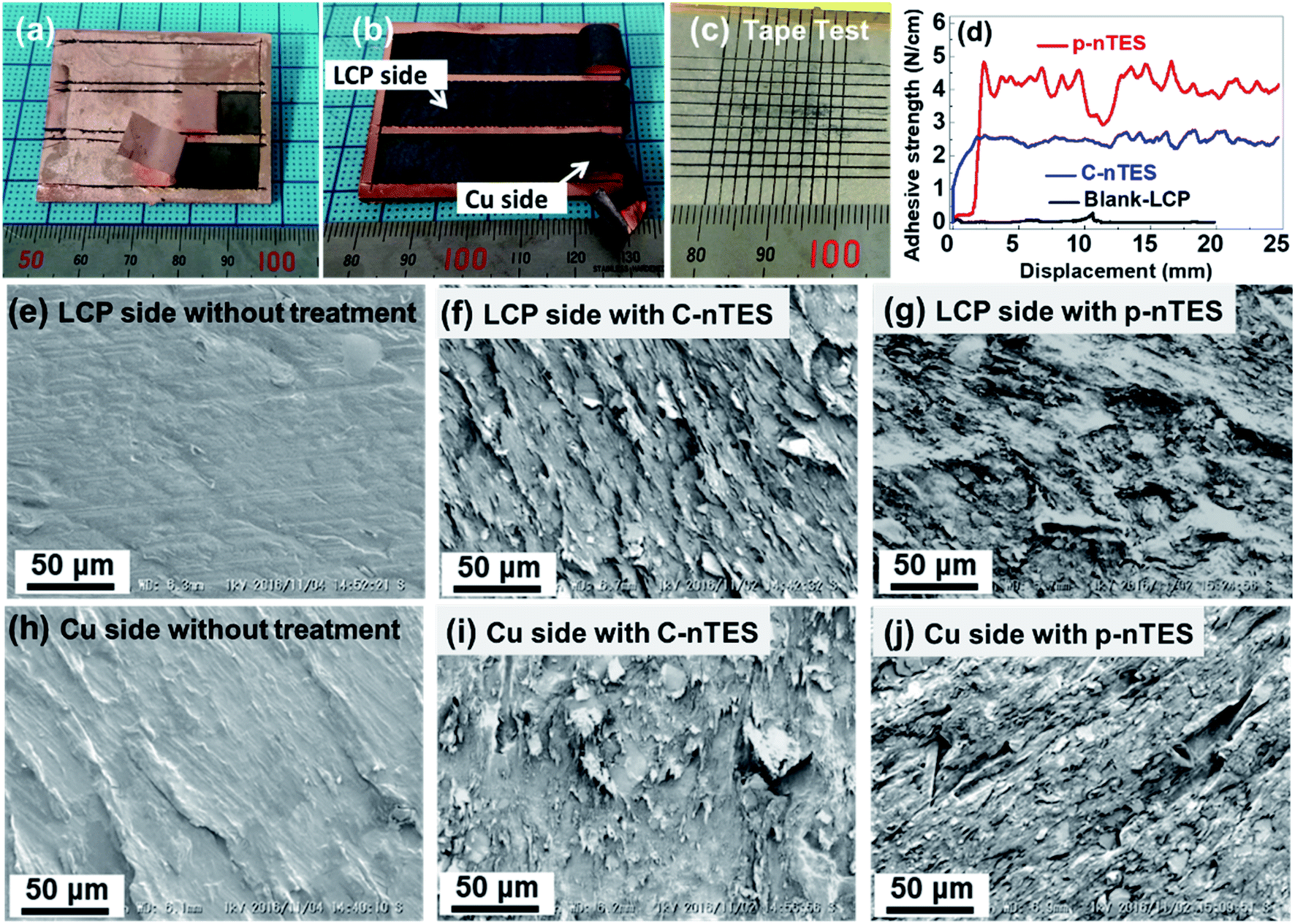 | ||
| Fig. 3 The adhesion of metal coatings on modified LCP: pictures of LCP samples (a) without or (b) with TES treatment after peeling off; (c) digital photos of Ag–LCP samples with TES treatment after a standard tape test; and (d) the typical adhesive strength of metal coatings on LCP. SEM images after peeling off: (e and h) without TES treatment, (f and i) after corona–nTES treatment, and (g and j) after pTES–nTES treatment; (e–g) LCP side and (h–j) coating side. | ||
SEM images of the LCP sides and Cu sides of species with no modification, and C–nTES and p–nTES modification are shown in Fig. 3e–j. When as-received LCP sheets were used for metallization, the LCP side and Cu side were found to have smooth surfaces after peeling off, whereas after C–nTES or p–nTES modifications, the surfaces showed roughened surfaces with some detachment traces. These results are consistent with the previously quantified adhesion strengths of metal coatings on different LCP surfaces. The detachment-like surface feathers, which are also observed from ABS and PET substrates (Fig. S4†), may be generated as a result of surface modification from molecular bonds between the metallic coating and polymer surface, and the peeling off process may lead to the breakage of the topmost modified surfaces of the LCP sheets30,38.
3.3. Surface feathers of the modified LCP
In order to figure out the metal coating adhesion mechanism on the LCP substrate, we identify the effects of each surface modification on the LCP surface. The surface morphology evolutions during these modification processes were investigated via SEM, as shown in Fig. 4. It worth noting that the LCP blank surface seems to be made of rough macrostructures with glossy micro-feathers (Fig. 4a and a1). With 0.1 wt% nTES self-assembly, the surface became smooth on the macroscale (Fig. 4b) but there was little change in the microscale view (Fig. 4b1). The number of captured microstructures can be simply improved by multiplying the number of assembly cycles to 3 or 5. The surfaces are found to be rougher with bumpy newly formed humps (Fig. 4b3 and b5), which are actually soft organic nTES adsorbed onto the LCP surface (Fig. 4b31 and b51), indicating that nTES filled the cavities on the LCP surface. As shown in Fig. 4c–f, macroscale uneven surfaces can be obtained upon increasing the nTES concentration from 0.1 to 3.0 wt% because the polar nTES molecules prefer to assemble onto active sites with lower free energies, leading to complicated surface architectures.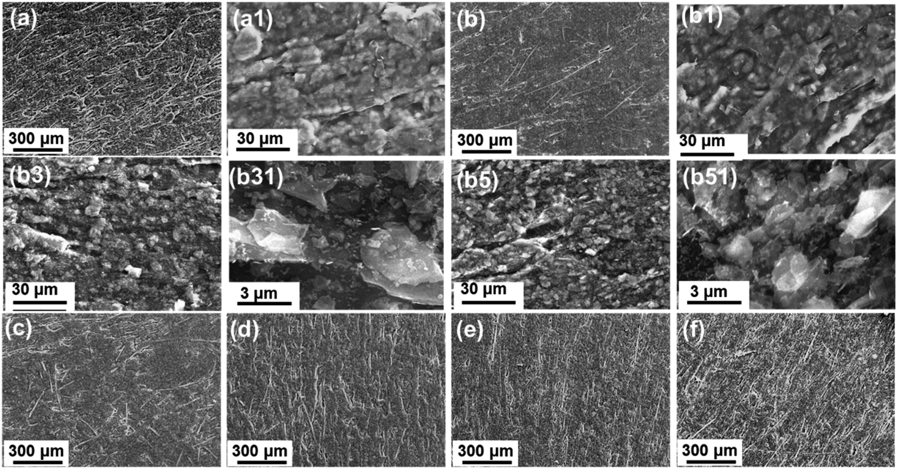 | ||
| Fig. 4 SEM images of the modified LCP surface morphologies: (a and a1) the blank substrate; different nTES concentrations of (b, b1, b3, b31, b5 and b51) 0.1, (c) 0.25, (d) 0.5, (e) 1.0, and (f) 3.0 wt%; and different numbers of self-assembly cycles of (b1) 1, (b3, b31) 3 and (b5, b51) 5, with a TES concentration of 0.1 wt%. | ||
3.4. Interfacial spectrum analysis
Fig. 5a shows the wettability of LCP surfaces after treatment. The contact angle of blank LCP is 66.3 ± 3.8°, and this decreased to 7.5 ± 0.5° after corona activation. However, the contact angle of pTES grafted LCP only slightly decreased to 57.8 ± 1.1°, and the contact angle was 41.8 ± 2.1° for the p–nTES surface. To gain further insight into the chemical compositions and chemical states of the modified LCP, XPS and FTIR were utilized to characterize the samples. Fig. 5b shows the survey XPS spectra of different LCP surfaces. Compared with the LCP substrate and pTES-treated and corona-activated surfaces, new peaks located at 398.8 and 163.4 eV are found in the C–nTES and p–nTES surface spectra corresponding to N 1s and S 2p, which are the common elements in nTES molecules (as shown in Fig. S2†). For further verification, the high-resolution N 1s and S 2p spectra of the C–nTES and p–nTES surfaces are presented in Fig. 5c, d and all XPS quantification data are gathered in Table 1. XPS high resolution spectra of the LCP substrate and pTES-treated and corona-activated surfaces are shown in Fig. S5–S7.†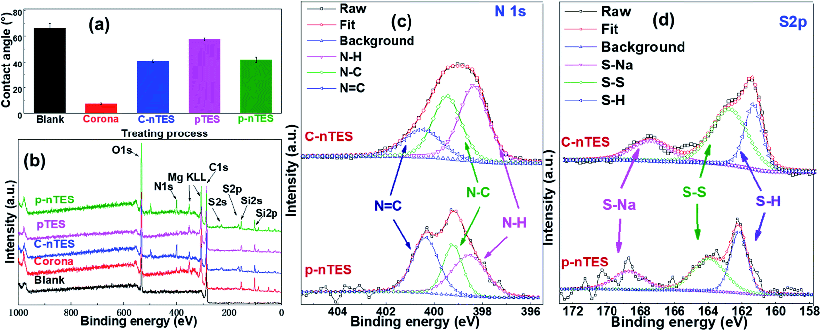 | ||
| Fig. 5 The surface properties of LCP substrates after different modification processes: (a) surface wettability; (b) XPS survey spectra; and high-resolution (c) N 1s and (d) S 2p XPS spectra. | ||
| Element | C–nTES | p–nTES | |||||||
|---|---|---|---|---|---|---|---|---|---|
| B.E. (eV) | FWHM | Peak area | Percent (at%) | B.E. (eV) | FWHM | Peak area | Percent (at%) | ||
| N 1s | NC |
400.4 | 1.81 | 1022.7 | 20.48% | 400.4 | 1.26 | 995.3 | 37.65% |
| N–C | 399.4 | 1.38 | 1775.0 | 35.54% | 399.2 | 0.93 | 671.8 | 25.41% | |
| N–H | 398.3 | 1.42 | 2197.1 | 43.99% | 398.5 | 1.45 | 976.4 | 36.94% | |
| S 2p | S–Na | 167.6 | 2.68 | 320.9 | 19.33% | 168.7 | 2.16 | 325.9 | 20.93% |
| S–S | 162.9 | 2.55 | 848.9 | 51.14% | 164.0 | 2.22 | 616.9 | 39.62% | |
| S–H | 161.5 | 1.27 | 490.3 | 29.53% | 162.2 | 1.17 | 614.3 | 39.45% | |
| C 1s | CO |
287.5 | 1.93 | 2169.3 | 30.14% | 288.4 | 2.21 | 1256.4 | 18.89% |
| C–O | 286.1 | 0.91 | 639.0 | 8.88% | 286.4 | 1.43 | 890.2 | 13.38% | |
| CC/C–C |
284.8 | 1.61 | 4389.9 | 60.99% | 284.8 | 1.45 | 4504.9 | 67.73% | |
| O 1s | O–Si | 532.5 | 1.45 | 1426.4 | 26.82% | 532.7 | 1.52 | 3561.5 | 37.23% |
| O–C | 531.8 | 1.20 | 2237.2 | 42.07% | 531.8 | 1.05 | 4101.8 | 42.87% | |
| O–H | 531.1 | 1.58 | 1654.2 | 31.11% | 531.1 | 1.17 | 1903.9 | 19.90% | |
| Si 2p | Si–OH | 102.5 | 1.28 | 362.0 | 42.46% | 102.3 | 1.23 | 407.2 | 29.06% |
| Si–O–Si | 101.8 | 1.19 | 490.6 | 57.54% | 103.3 | 1.74 | 993.9 | 70.94% | |
Deconvolution of the N 1s spectra from modified LCP surfaces (Fig. 5c) results in a few characteristic peaks centered at 400.4, 399.4 and 398.3 eV, which can be assigned to NC, N–C and N–H bonds, respectively. It is noteworthy that all the aforementioned peaks from the LCP surface appear in the N 1s narrow scan of C–nTES and p–nTES surfaces, but the peak at 400.4 eV (NC) is diminished in the case of the C–nTES surface. From the fitting parameters of N 1s (Table S1†), the proportion of this peak (NC) on the C–nTES surface is 20.48%, but it is 37.65% for the p–nTES surface. This is because NC bonds also appear in p-TES molecules (Fig. S2a†), leading to more NC bonds on the p–nTES surfaces. On the other hand, the narrow scan S 2p spectra (Fig. 5d) evidently confirm the presence of –SH groups on the C–nTES and p–nTES surfaces. The S 2p spectra can be deconvoluted into peaks centered at 167.6 eV (S–Na), 162.9 eV (S–S) and 161.5 eV (S–H). In addition, the high-resolution spectra raw curves from the C–nTES surface are smoother and show stronger signal intensities than those from the p–nTES surface, suggesting that more TES molecules assemble on corona-activated LCP.
Furthermore, other narrow scan C 1s, O 1s and Si 2p spectra are depicted in Fig. S8,† and the fitting parameters of these peaks are summarized in Table 1. Compared with the C–nTES surface, the specific peaks for the p–nTES surface are found to be blue-shifted: from 287.5 to 288.4 eV for CO in the C 1s spectrum (Fig. S8a and d†); from 532.5 to 532.7 eV for O–Si in the O 1s spectrum (Fig. S8b and e†); and from 102.5 to 102.8 eV for Si–O–Si in the Si 2p spectrum (Fig. S8c and f†). In particular, for the O 1s and Si 2p cases, the proportions of O–Si and Si–O–Si increase to 37.23% and 70.94%, from 26.82% and 57.54%, respectively. This means that p–nTES treatment is more efficient for modifying the LCP surface.
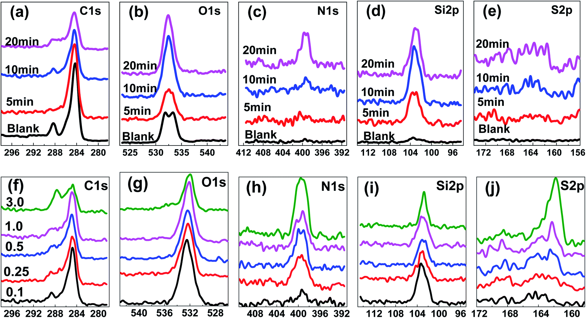
Fig. 6 shows XPS high-resolution spectra from LCP surfaces as a function of nTES self-assembly time and dosage. From Fig. 6a–e, the peak shapes and heights are different as the assembly time increases from 0 to 20 min, even for C 1s and O 1s (Fig. 6a and b). It is noteworthy that distinct N 1s and Si 2p peaks are found from the nTES self-assembly surfaces after 20 min (Fig. 6c and d) compared with the blank surface, meaning that the nTES self-assembly procedure is useful for decorating the LCP surface. However, because of the small amount of S in nTES molecules (Fig. S2b†), the amount of S element on the surface is too low to form an obvious and sharp peak, and instead several rough bulges appear (Fig. 6e). Increasing the dosage of nTES to 1.0 and 3.0 wt% will result in apparent S 2p peaks, as shown in Fig. 6j, due to a sufficiently large quantity of nTES assembling on the LCP surface. In addition, IR spectra of LCP treated with different UV radiation and nTES dosages are presented in Fig. S9.† Specific peaks that correspond to Si–C, Si–O–Si and CN are clearly found on these surfaces, and the intensities will increase with treatment dosage.
 | ||
| Fig. 6 XPS high-resolution spectra of LCP surfaces with different (a–e) nTES self-assembly times of 5–20 minutes at 0.1 wt% and (f–j) dosages of 0.1–3.0 wt% with a time of 20 min. | ||
3.5. Formation mechanism of molecular bonding
Metal/polymer interface adhesion mechanisms can be estimated based on interfacial structures and molecular interfacial interactions.39 Combining the interfacial morphology and spectrum analysis data, Fig. 7a shows the chemical reaction steps for the molecules involved in these two methods. For the C–nTES surface, corona treatment led to –OH groups on the LCP surface, as shown in Fig. 7a. Silane with thiol groups can be fixed onto the surface via the dehydration condensation reaction between the –OH and silane groups, which has been proved from the XPS results in Fig. 5. After metallization, the outer thiols groups can react with deposited silver to form S–Ag bonds. As a consequence, molecular bonds are successfully constructed between the metal layer and polymer surface, as shown in Fig. S10.†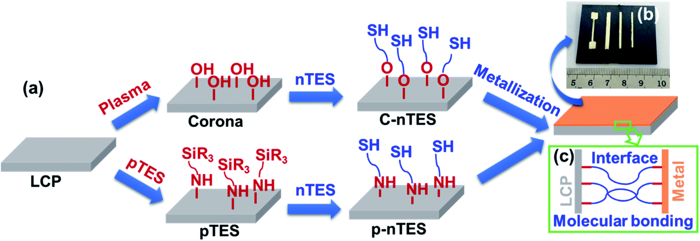 | ||
| Fig. 7 (a) A schematic illustration showing the formation of a molecularly bonded interface between the polymer and metal coating; the procedures for constructing thiol groups and Ag coatings on liquid crystal polymer (LCP) surfaces, including corona treatment (shorted to Corona), nTES self-assembly on corona-activated LCP (C–nTES), UV-assisted pTES grafting (pTES), and nTES self-assembly on pTES grafted LCP (pTES–nTES). (b) The prepared Ag patterns on LCP. (c) A schematic drawing of the molecular bonding interface between LCP and the metal. | ||
Azides have been extensively utilized for functionalizing materials and surfaces due to their ability to be easily converted to nitrene, which is a nitrogen species containing six highly reactive valence electrons that is capable of inserting C–H bonds onto substrates via photolysis or thermolysis.40–42 In this work, azides were used to functionalize the LCP surface. For the p–nTES surface, the azide group of pTES was activated via UV light to convert it to the highly reactive triazinyl nitrene, which can covalently bond to the neighboring hydrocarbons on the polymer surface, as proved by the XPS results in Fig. 5 and S7.† nTES bonded with the fixed pTES via forming Si–O–Si network linkages through the intermolecular condensation reaction of two silanol groups (as shown in Fig. 5 and S8†). Therefore, the constructed molecular bonding between the polymer substrate and metal layer is composed of pTES and nTES, as shown in Fig. S11.† As described above, the formation mechanism of molecular bonding has been illustrated in Fig. 7a. By using a mask, Ag metallic patterns can be deposited onto LCP easily, as shown in Fig. 7b. We expect that robust molecular bonding can form at the interface of the LCP sheet and metallic coating, thus providing strong conductive pattern adhesion on the polymer surface (Fig. 7c).
4. Conclusions
In summary, we have demonstrated strong interfacial nanoconnections based on metallic patterns on LCP that were fabricated via a molecular bonding approach, which includes UV-assisted pTES grafting and nTES self-assembly. The interfacial molecular nanolayers have a thickness of 10 nm and are identified using nano-AFM-IR studies. Due to the successful molecular bonding modification, interfacial adhesion is sufficiently improved; in particular, the peel-related breakage sites will be located in the modified layers on the LCP surface beneath the interface after the metallic coatings are peeled off. Based on XPS, IR and SEM results, the molecular bonding mechanism has been revealed: UV-assisted pTES grafting and nTES self-assembly lead to the construction of interfacial molecular architectures, which provide connecting bridges between the metallic patterns and polymer surface. Such in-depth interfacial studies offer insight into interfacial adhesion, which can impact the development of metal/polymer composite systems and will continue to push the improvement of flexible devices.Author contributions
The manuscript was written through contributions from all the authors. All authors have given approval to the final version of the manuscript.Funding sources
The authors gratefully acknowledge financial support from the Guangdong Basic and Applied Basic Research Foundation (No. 2019A15150101011282), the Fundamental Research Funds for the Central Universities (21619336), and the Open Funds of National Engineering Research Center of Near-Net-Shape Forming for Metallic Materials (2019008).Conflicts of interest
There are no conflicts to declare.References
- X. Dai, J. Wu, Z. Qian, H. Wang, J. Jian, Y. Cao, M. H. Rummeli, Q. Yi, H. Liu and G. Zou, Sci. Adv., 2016, 2, e1601574 CrossRef PubMed.
- S. Park, S. W. Heo, W. Lee, D. Inoue, Z. Jiang, K. Yu, H. Jinno, D. Hashizume, M. Sekino, T. Yokota, K. Fukuda, K. Tajima and T. Someya, Nature, 2018, 561, 516–521 CrossRef CAS PubMed.
- S. Chen, M. Su, C. Zhang, M. Gao, B. Bao, Q. Yang, B. Su and Y. Song, Adv. Mater., 2015, 27, 3928–3933 CrossRef CAS PubMed.
- J.-W. Liu, J.-L. Wang, Z.-H. Wang, W.-R. Huang and S.-H. Yu, Angew. Chem., Int. Ed., 2014, 53, 13477–13482 CrossRef CAS PubMed.
- Y.-Z. Zhang, Y. Wang, T. Cheng, L.-Q. Yao, X. Li, W.-Y. Lai and W. Huang, Chem. Soc. Rev., 2019, 48, 3229–3264 RSC.
- M. Yu, H. Wan, L. Cai, J. Miao, S. Zhang and C. Wang, ACS Nano, 2018, 12, 11572–11578 CrossRef CAS PubMed.
- Q. Wang, Y. Yu, J. Yang and J. Liu, Adv. Mater., 2015, 27, 7109–7116 CrossRef CAS PubMed.
- S. Park, M. Vosguerichian and Z. Bao, Nanoscale, 2013, 5, 1727–1752 RSC.
- H. Kang, S. Jung, S. Jeong, G. Kim and K. Lee, Nat. Commun., 2015, 6, 6503 CrossRef CAS PubMed.
- C. Cai and R. H. Dauskardt, Nano Lett., 2015, 15, 6751–6755 CrossRef CAS PubMed.
- Z. Liu, X. Wang, D. Qi, C. Xu, J. Yu, Y. Liu, Y. Jiang, B. Liedberg and X. Chen, Adv. Mater., 2017, 29, 1603382 CrossRef PubMed.
- P. Li, Y. Zhang and Z. Zheng, Adv. Mater., 2019, 31, e1902987 CrossRef PubMed.
- X. Hu, Y. Dou, J. Li and Z. Liu, Small, 2019, 15, 1804805 CrossRef PubMed.
- Z. Wang, R. Xing, X. Yu and Y. Han, Nanoscale, 2011, 3, 2663–2678 RSC.
- Y. Wang, H.-J. Yang, H.-Z. Geng, Z.-C. Zhang, E.-X. Ding, Y. Meng, Z.-J. Luo, J. Wang, X.-M. Su and S.-X. Da, J. Mater. Chem. C, 2015, 3, 3796–3802 RSC.
- C. Pang, G.-Y. Lee, T.-i. Kim, S. M. Kim, H. N. Kim, S.-H. Ahn and K.-Y. Suh, Nat. Mater., 2012, 11, 795–801 CrossRef CAS PubMed.
- J. H. Park, S. Han, D. Kim, B. K. You, D. J. Joe, S. Hong, J. Seo, J. Kwon, C. K. Jeong, H.-J. Park, T.-S. Kim, S. H. Ko and K. J. Lee, Adv. Funct. Mater., 2017, 27, 1701138 CrossRef.
- C. Huang, L. Kang, N. Zhang, S. Wan, X. Zhou and J. Zhang, ACS Appl. Mater. Interfaces, 2019, 11, 38303–38312 CrossRef CAS PubMed.
- S. Baik, H. J. Lee, D. W. Kim, J. W. Kim, Y. Lee and C. Pang, Adv. Mater., 2019, 31, 1803309 CrossRef PubMed.
- M. Ha, S. Lim, J. Park, D.-S. Um, Y. Lee and H. Ko, Adv. Funct. Mater., 2015, 25, 2841–2849 CrossRef CAS.
- K. N. Kim, S. M. Lee, A. Mishra and G. Y. Yeom, Thin Solid Films, 2016, 598, 315–334 CrossRef CAS.
- A. Laskarakis, S. Logothetidis, S. Kassavetis and E. Papaioannou, Thin Solid Films, 2008, 516, 1443–1448 CrossRef CAS.
- M. Hu, Q. Guo, T. Zhang, S. Zhou and J. Yang, ACS Appl. Mater. Interfaces, 2016, 8, 4280–4286 CrossRef CAS PubMed.
- J. Cai, C. Zhang, A. Khan, L. Wang and W. D. Li, ACS Appl. Mater. Interfaces, 2018, 10, 28754–28763 CrossRef CAS PubMed.
- H. Zhang, P. Zhang, H. Zhang, X. Li, L. Lei, L. Chen, Z. Zheng and Y. Yu, ACS Appl. Mater. Interfaces, 2018, 10, 28963–28970 CrossRef CAS PubMed.
- Z. Zhang and J. Liu, J. Mater. Chem. C, 2016, 4, 4218–4225 RSC.
- S. Ma, X. Zhang, B. Yu and F. Zhou, NPG Asia Mater., 2019, 11, 24 CrossRef.
- Y.-T. Kwon, Y.-S. Kim, Y. Lee, S. Kwon, M. Lim, Y. Song, Y.-H. Choa and W.-H. Yeo, ACS Appl. Mater. Interfaces, 2018, 10, 44071–44079 CrossRef CAS PubMed.
- Q. Qiang, J. Qin, Y. Ma, Z. Wang and C. Zhao, ACS Appl. Mater. Interfaces, 2019, 11, 5517–5525 CrossRef CAS PubMed.
- D. X. Chen, Y. Zhang, T. Bessho, J. Sang, H. Hirahara, K. Mori and Z. X. Kang, Chem. Eng. J., 2016, 303, 100–108 CrossRef CAS.
- Y. Qin, M. M. R. Howlader, M. J. Deen, Y. M. Haddara and P. R. Selvaganapathy, Sens. Actuators, B, 2014, 202, 758–778 CrossRef CAS.
- J. Jeong, K. S. Min and S. J. Kim, Microelectron. Eng., 2019, 216, 111096 CrossRef CAS.
- Y. Qin, H.-J. Kwon, A. Subrahmanyam, M. M. R. Howlader, P. R. Selvaganapathy, A. Adronov and M. J. Deen, Mater. Lett., 2016, 176, 68–70 CrossRef CAS.
- H.-l. Kao, C.-L. Cho, L.-C. Chang, C.-S. Yeh, B.-W. Wang and H.-C. Chiu, Thin Solid Films, 2013, 544, 64–68 CrossRef CAS.
- G.-T. Hwang, D. Im, S. E. Lee, J. Lee, M. Koo, S. Y. Park, S. Kim, K. Yang, S. J. Kim, K. Lee and K. J. Lee, ACS Nano, 2013, 7, 4545–4553 CrossRef CAS PubMed.
- A. Dazzi and C. B. Prater, Chem. Rev., 2017, 117, 5146–5173 CrossRef CAS PubMed.
- D. Chen, Z. Kang, H. Hirahara, S. Aisawa and W. Li, Appl. Surf. Sci., 2019, 479, 368–374 CrossRef CAS.
- D. X. Chen, Z. X. Kang and T. Bessho, J. Ind. Eng. Chem., 2017, 52, 73–81 CrossRef CAS.
- C. Zhang, J. Hankett and Z. Chen, ACS Appl. Mater. Interfaces, 2012, 4, 3730–3737 CrossRef CAS PubMed.
- S. Xie, S. A. Lopez, O. Ramström, M. Yan and K. N. Houk, J. Am. Chem. Soc., 2015, 137, 2958–2966 CrossRef CAS PubMed.
- L.-H. Liu and M. Yan, Acc. Chem. Res., 2010, 43, 1434–1443 CrossRef CAS PubMed.
- C.-W. Lin, S. Aguilar, E. Rao, W. H. Mak, X. Huang, N. He, D. Chen, D. Jun, P. A. Curson, B. T. McVerry, E. M. V. Hoek, S.-C. Huang and R. B. Kaner, Chem. Sci., 2019, 10, 4445–4457 RSC.
Footnote |
| † Electronic supplementary information (ESI) available: Molecular structures of LCP, pTES and nTES; element proportions from EDS; the typical adhesive strengths of metal coatings on LCP substrates following different surface treatments; XPS high-resolution C 1s, O 1s and Si 2p spectra; IR spectra with different UV radiation and nTES dosages; a flow diagram showing the creation of molecular bonding in the C–nTES and p–nTES cases. See DOI: 10.1039/d0na00176g |
| This journal is © The Royal Society of Chemistry 2020 |