DOI:
10.1039/D0NA00175A
(Paper)
Nanoscale Adv., 2020,
2, 2577-2586
A hierarchical SnS@ZnIn2S4 marigold flower-like 2D nano-heterostructure as an efficient photocatalyst for sunlight-driven hydrogen generation†
Received
1st March 2020
, Accepted 16th April 2020
First published on 16th April 2020
Abstract
Herein, we report the in situ single-step hydrothermal synthesis of hierarchical 2D SnS@ZnIn2S4 nano-heterostructures and the examination of their photocatalytic activity towards hydrogen generation from H2S and water under sunlight. The photoactive sulfides rationally integrate via strong electrostatic interactions between ZnIn2S4 and SnS with two-dimensional ultrathin subunits, i.e. nanopetals. The morphological study of nano-heterostructures revealed that the hierarchical marigold flower-like structure is self-assembled via the nanopetals of ZnIn2S4 with few layers of SnS nanopetals. Surprisingly, it also showed that the SnS nanopetals with a thickness of ∼25 nm couple in situ with the nanopetals of ZnIn2S4 with a thickness of ∼25 nm to form a marigold flower–like assembly with intimate contact. Considering the unique band gap (2.0–2.4 eV) of this SnS@ZnIn2S4, photocatalytic hydrogen generation from water and H2S was performed under sunlight. SnS@ZnIn2S4 exhibits enhanced hydrogen evolution, i.e. 650 μmol h−1 g−1 from water and 6429 μmol h−1 g−1 from H2S, which is much higher compared to that of pure ZnIn2S4 and SnS. More significantly, the enhancement in hydrogen generation is 1.6–2 times more for H2S splitting and 6 times more for water splitting. SnS@ZnIn2S4 forms type I band alignment, which accelerates charge separation during the surface reaction. Additionally, this has been provoked by the nanostructuring of the materials. Due to the nano-heterostructure with hierarchical morphology, the surface defects increased which ultimately suppresses the recombination of the electron–hole pair. The above-mentioned facts demonstrate a significant improvement in the interface electron transfer kinetics due to such a unique 2D nano-heterostructure semiconductor which is responsible for a higher photocatalytic activity.
1. Introduction
Due to rapid fossil fuel consumption, increasing energy demands because of modern civilization growth, global warming, and the greenhouse effect, there have been serious challenges posed to the scientific community worldwide in the 21st century.1,2 Among all potential solutions being considered, hydrogen (H2) is one of the promising candidates for green energy owing to its high energy density, non-polluting nature, easy transportability and zero hazardous gas emission.3 Hydrogen generation from water and H2S splitting using solar energy has attracted considerable attention for sustainable and renewable energy research.4,5 It is a crucial time that highly proficient, durable, eco-friendly and low-cost alternative energy production is a significant goal to solve energy and environmental problems. In this context, semiconductor-based photocatalytic H2 generation from water splitting under sunlight is a promising technology for future fuel.6,7
Sunlight-mediated hydrogen evolution from water splitting (solar energy to chemical fuel) by breaking of chemical bonds, similar to photosynthesis, i.e. (HER) (HER: 2H+ + 2e− → H2), required large Gibb's free energy change, i.e. 273 kJ mol−1, which has to be supplied to initiate the reaction.8 This can be made possible using a narrow band gap semiconductor that absorbs maximum light upon exposure to sunlight. However, to meet the ideal criteria, semiconductors must satisfy several principal requirements. These include good solar light absorption capability, adequate band gap and band edge position with sufficient driving potential, efficient charge transfer kinetics, surface catalytic proton reduction potential, and minimal photo corrosion.9,10 The pioneering discovery was done by Fujishima and Honda using a TiO2 electrode for hydrogen generation.11 Similar to TiO2, several alternative binary metal oxide photocatalysts such as Nb2O5,12 Ta2O5,13 and ZnO14 were developed and examined for hydrogen generation. However, their photocatalytic activity is not good enough for commercial purposes, due to low conductance, unsuitable indirect band gap, inadequate wide band gap range of light absorption and insufficient charge separation that leads to a rapid charge carrier's recombination process, with concomitant diminishing of their photocatalytic activity.15 To overcome these limitations, previous reports have shown that anion doping in TiO2 catalysts tunes the band gap in the visible region, to improve the photocatalytic activity,16 but doping sites act as recombination centers which retard the photocatalytic activity. Some reports also showed that loading of noble metals such as Ag, Au, Pt, and Rh or co-catalysts on the surface of the passive oxide semiconductor enhances absorption towards longer wavelengths, but the widespread use of noble metals is not economically feasible.17
Recently, 2D transition metal dichalcogenides (TMDs), typical II–III2–VI4 semiconductors, are a large family of layered materials that have gained extensive interest due to their unique physicochemical properties and promising applications. 2D TMDs compared with 3D transition metal oxides possess a narrow band gap (1.23–3.0 eV), having a high specific surface area, and they can significantly inhibit charge carrier recombination; therefore, they have great potential for solar-light harvesting.18,19 To date, various 2D chalcogenides such as CdS,20 MoS2,21 In2S3,22 ZnS,23 and ZnSe,24 have been reported and studied for good photocatalytic activity. However, these sulfides are having stability issues along with that photo-corrosion problem. To solve photo-corrosion problems, ternary sulfides such as CdIn2S4,25 ZnIn2S4,26 and CdMoS4 (ref. 27) have been explored for improved stability and enhanced photocatalytic activity. Among all the reported ternary sulfides, ZnIn2S4 is a layered structure that has been proved to be a prominent visible light active catalyst due to its suitable band gap (2.3–2.5 eV) and excellent photocatalytic activity with stability.28 In the past, various attempts have been made to enhance the photocatalytic activity of ZnIn2S4, more specifically coupling of two individual semiconductors such as ZnIn2S4/TiO2,29 ZnIn2S4/CdS,30 and ZnIn2S4/ZnFe2S4.31 With this motivation, we prepared a new SnS@ZnIn2S4 hybrid semiconductor by coupling ZnIn2S4 and SnS. The main aim of this semiconductor is to promote an interparticle electron transfer mediator to obtain two-step excitations, known as Z-scheme electron transfer. To the best of our knowledge, no previous work has reported on 3D hierarchical ZnIn2S4 coupled with SnS for photocatalytic application study. In this context, we successfully fabricated in situ SnS@ZnIn2S4 nanocomposite heterostructure photocatalysts by a facile hydrothermal method. The strong electrostatic interaction between negatively charged SnS and positively charged Zn and In ions of ZnIn2S4 facilitates close contact between ZnIn2S4 and SnS. Moreover, type I band alignment is designed in 2D ultrathin ZnIn2S4 and SnS, which provides highly efficient charge separation. The SnS provides active sites and acts as a co-catalyst for hydrogen generation.
In this work, we synthesized a SnS@ZnIn2S4 heterostructure photocatalyst and examined it for hydrogen generation under natural solar-light irradiation. It was found that SnS@ZnIn2S4 exhibits significantly enhanced photocatalytic activity for hydrogen evolution. Furthermore, the synergy between ZnIn2S4 and SnS and the possible mechanism underlying improved photocatalytic activity were studied systematically.
2 Experimental section
Zinc nitrate hexahydrate (Zn(NO3)2·6H2O), indium nitrate (In(NO3)3·4H2O), tin chloride dihydrate (SnCl2·2H2O) and thiourea (N2H4CS) used for the preparation of catalysts were of analytical grade (SD-Fine-Chem Limited, India) and used without further purification.
2.1 Synthesis of ZnIn2S4 and SnS@ZnIn2S4
All the chemicals used for the synthesis of SnS@ZnIn2S4 were of analytical grade and used without further purification. SnS@ZnIn2S4 photocatalysts were synthesized by a hydrothermal method, and the procedure is briefly described as follows: first, 1 mole of zinc nitrate hexahydrate (Zn (NO3)2·6H2O) (99.99%) and 2 moles of indium nitrate (In(NO3)3·4H2O) (99.99%) were mixed in 50 mL water in a beaker (a). Similarly, 1 wt% tin chloride solution was prepared in 10 mL double-distilled water in another beaker (b) and added to the above mixture (a). The clear solution was then transferred to a 200 mL Teflon autoclave and kept at 160 °C for 30 h in an electric oven. As the synthesized catalyst was washed several times with absolute ethanol and deionized water, a yellow-colored powder was obtained. This samples were marked as S1 for pure ZnIn2S4, S2 1% SnS@ZnIn2S4, S3 2% SnS@ZnIn2S4, and S4 3% SnS@ZnIn2S4 and used for further analyses and comparison thereafter. Similarly, different concentrations of tin chloride solution, namely, 1 wt%, 2 wt%, and 3 wt% respectively, were prepared, and the same procedure as mentioned above was followed to synthesize other samples. Hence, four samples were prepared for comparative purposes and each sample so obtained is represented and labeled as S1 for ZnIn2S4, and 1% SnS@ZnIn2S4, 2% SnS@ZnIn2S4, 3% SnS@ZnIn2S4 as S2, S3, and S4, respectively, for convenience.
2.2 Photocatalytic study
2.2.1 Photocatalytic hydrogen generation from water.
The photochemical reaction was carried out in a 70 mL total volume air-tight cylindrical quartz reactor with a cooling jacket for water circulation. All the reactions were carried out under ambient conditions with natural sunlight on sunny days (March to May months) between 10 am to 3 pm at Pune, located in the Maharashtra state of India. The intensity of solar light was measured using a digital Lux meter. The measured average intensity of solar light reaching the surface of the earth was 145![[thin space (1/6-em)]](https://www.rsc.org/images/entities/char_2009.gif) 000 Lux. In a typical photocatalytic experiment, 15 mg of the photocatalyst was dispersed in 25 mL total volume containing 20% methanol (v/v) in aqueous solution. The free space only of photoreactor made airtight with rubber septum followed by ultrasonication for 5 min for the uniform dispersion of catalyst. The solution mixture was then purged with ultra-high-purity nitrogen gas (UHP-99.999%) to remove all the gases in the headspace of the reactor and dissolved oxygen from the reaction mixture. Before and after irradiation with solar light, the gas in the free space of the reactor was analyzed by gas chromatography (GC). The generated gas was analyzed immediately by GC with a specific time interval.
000 Lux. In a typical photocatalytic experiment, 15 mg of the photocatalyst was dispersed in 25 mL total volume containing 20% methanol (v/v) in aqueous solution. The free space only of photoreactor made airtight with rubber septum followed by ultrasonication for 5 min for the uniform dispersion of catalyst. The solution mixture was then purged with ultra-high-purity nitrogen gas (UHP-99.999%) to remove all the gases in the headspace of the reactor and dissolved oxygen from the reaction mixture. Before and after irradiation with solar light, the gas in the free space of the reactor was analyzed by gas chromatography (GC). The generated gas was analyzed immediately by GC with a specific time interval.
2.3 Sample characterization
The phase formation and crystallite size of all synthesized samples were estimated using an X-ray diffractometer (XRD-D8, Advance, Bruker-AXS) with Ni-filtered Cu-Kα radiation (λ = 1.5418 Å). The optical properties of the bare and Au-loaded samples were studied using a UV-vis-DRS spectrophotometer (UV 2600 spectrometer, Lambda-950, PerkinElmer) in the spectral range of 200–800 nm. The surface morphology was characterized using a field emission scanning electron microscope (FESEM; Hitachi, S-4800 II) and a field emission transmission electron microscope (FETEM; JEM-2000 FS). Image processing and interplanar distance (d) evaluation were performed using the micrograph Gatan software. The Brunauer–Emmett–Teller (BET) technique was employed to calculate the surface area from the adsorption branch (NOVA Touch, surface area and pore size analyzer, Quanta chrome instrument). Surface characterization of all SnS@ZnIn2S4 samples was carried out using a X-ray photoelectron spectrometer (XPS, ESCA-3000, VG Scientific Ltd.) at a pressure of >1 × 10⁻⁹ Torr. The general scan C 1s, S 2p, In 3d, Sn 3d, and Zn 2p core level spectra were recorded with non-monochromatized Mg-Kα radiation (photon energy – 1253.6 eV). Baseline correction and peak fitting for all the samples were performed using the software package XPS peak-41. The core-level binding energies (BEs) were aligned with respect to the C 1s binding energy of 285 eV. The collected gas sample was analyzed using a gas chromatography system (Shimadzu GC-2014) with a portapak-Q packed column coupled with a TCD detector and nitrogen (N2-UHP) as a carrier gas.
3. Results and discussion
3.1 Structural study
A facile low-temperature one-step hydrothermal method was employed for the in situ preparation of SnS@ZnIn2S4 nano-heterostructures. Fig. 1 (S1–S4) shows powder X-ray diffraction patterns of the as-prepared ZnIn2S4 and SnS@ZnIn2S4 nanocomposites. Fig. 1 (S1) and (S2–S4) shows the X-ray diffraction patterns of pure ZnIn2S4 and SnS@ZnIn2S4. Major diffraction peaks located at 2θ values 21.5, 27.6 and 47.1° could be attributed to the reflection of the (0 0 6) (1 0 2) and (1 1 0) planes of hexagonal ZnIn2S4 which matches well with JCPDS card no-01-072-0773.32Fig. 1 (S2–S4) shows the XRD pattern of SnS@ZnIn2S4 samples in which additional peaks are observed with the co-existence of both ZnIn2S4 and SnS phases. The major diffraction peaks located at 2θ values 22.0, 30.4, 34.5, 39.0 and 53.4° could be attributed to the reflection of the (0 0 1) (0 0 1) (2 1 1) (3 1 1) and (6 0 1) planes of orthorhombic SnS33 (JCPDF card no-01-073-1859), demonstrating the successful formation of the SnS@ZnIn2S4 composite material. The XRD pattern of pure SnS is shown in ESI (Fig. I).† Impurity peaks of binary sulfides such as ZnS and In2S3 could not be observed, which confirms the phase purity of the as-prepared samples. Although SnS has a great influence on the surface morphology of ZnIn2S4, it does not affect the crystal structure of ZnIn2S4. Furthermore, it is observed that the diffraction peak intensity and crystallinity of both SnS and ZnIn2S4 increase with the increase in the content of SnS from (S2–S4). Besides, the relative intensity of the (1 0 4) plane increases with the increase in the concentration of SnS and diminished the relative intensity of the (0 0 6) plane of ZnIn2S4. It is evident that no significant shift in the peak positions was observed in each as-synthesized SnS@ZnIn2S4 sample, signifying that the deposited SnS is not incorporated into the lattice of ZnIn2S4.
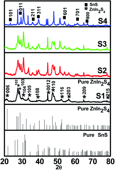 |
| | Fig. 1 X-ray diffraction patterns of (S1) pure ZnIn2S4, (S2) 1% SnS@ZnIn2S4, (S3) 2% SnS@ZnIn2S4 and (S4) 3% SnS@ZnIn2S4 sample photocatalysts. | |
3.2 Surface and morphological studies
Fig. 2 shows a representative FE-SEM image of pure ZnIn2S4 and SnS@ZnIn2S4 nano-heterostructures. Fig. 2(a and b) shows the morphology of pure ZnIn2S4, in which the uniform marigold flower-like structure of ZnIn2S4 (3–5 μm) comprised the self-assembly of nanopetals under hydrothermal conditions. Surprisingly, the diameter of the petals is in the micron range; however, the thickness of the petal is few nanometers, i.e. ∼25 nm. The aspect ratio of one petal is more than 500 nm, which clearly shows the enhanced surface area of a single flower. Fig. 2(c and d) shows the surface morphology of 1% SnS-loaded ZnIn2S4, in which the marigold flower-like structure (2.4–5 μm) is composed of nanopetals of SnS and ZnIn2S4. The thickness of the twin nanopetals is measured to be 20–25 nm, and it is around 50 nm for coupled nanopetals of the nano-heterostructure. We can see the parallel growth of SnS and ZnIn2S4 petals in composed marigold flower–like structures (Fig. 2(d)). The growth of the flowers has been accelerated with SnS. The growth orientation has been changed significantly with the increase in the content of SnS, as shown in Fig. 2(e and f) (2–5 μm). The surface morphology of 2% loaded SnS on ZnIn2S4 clearly shows a porous marigold flower-like structure assembled with thin petals of SnS and ZnIn2S4.
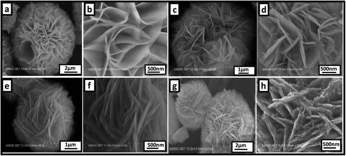 |
| | Fig. 2 Representative FE-SEM images of (a and b) pure ZnIn2S4, (c and d) 1% SnS@ZnIn2S4, (e and f) 2% SnS@ZnIn2S4 and (g and h) 3% SnS@ZnIn2S4 sample photocatalysts. | |
The length of the nanopetals is in the range of 500–1000 nm, and the thickness is measured to be 50 nm. Significantly, here also we can see the twin petals, i.e. SnS and ZnIn2S4. Fig. 2(f) shows a thickness of 25 nm for each of the petals. Fig. 2(g and h) shows the morphology of 3% SnS-loaded ZnIn2S4, which shows distorted flowers (2–7 μm). Furthermore, it was observed that these flowers are made up of thick (50 nm) SnS and ZnIn2S4 nanopetals along with a cluster of SnS (5–10 nm) nanoparticles.
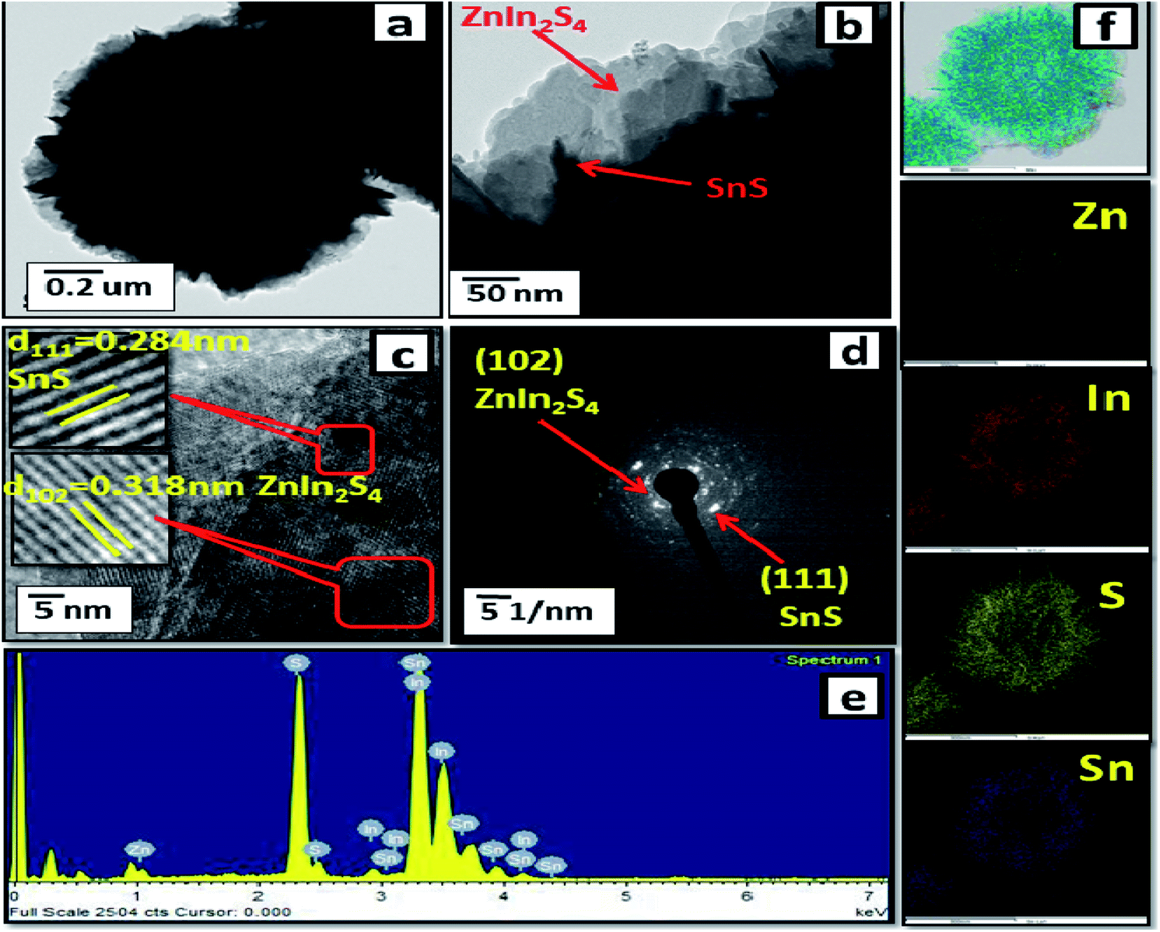
Furthermore, FE-TEM investigations (as shown in Fig. 3(a–d)) were performed to determine the morphology and crystalline nature of the SnS@ZnIn2S4 nano-heterostructure. Fig. 3(a and b) shows the TEM images of the SnS@ZnIn2S4 nanopetals with an ordered uniform structure. The ultrathin ZnIn2S4 nanopetals are coupled with nanopetals of SnS, and they form a SnS@ZnIn2S4 nano-heterostructure, which is in good agreement with the XRD data. Significantly, very thin petals of ZnIn2S4 and SnS of a few nanometer thickness were observed. Fig. 3(c) shows the HRTEM images of SnS@ZnIn2S4 taken at the edge part, which depicts a lattice spacing of 0.318 nm that could be assigned to the (1 0 2) plane of hexagonal ZnIn2S4 and 0.284 nm assigned to the (1 1 1) plane of SnS matching with the XRD results. The selected area electron diffraction (SAED) pattern shown in Fig. 3(d) indicates the as-synthesized SnS@ZnIn2S4 nanocomposite of crystalline nature. Fig. 3(e) shows the EDAX spectra that confirm the co-existence of Zn, In, Sn and S elements. Furthermore, Fig. 3(f) also shows the STEM elemental mapping, which confirms the existence of Zn, In, Sn and S. The corresponding elemental mapping of Zn, In, S and Sn are identical with each other, which illustrates the attractive porous nature. Hence, it is reasonable to believe that the 2D SnS@ZnIn2S4 heterostructure with intimate interfacial contact also shows synergy between SnS and ZnIn2S4 micropetals.
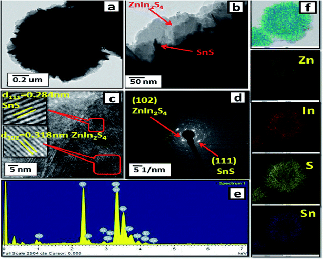 |
| | Fig. 3 FE-TEM images (a and b), (c) HRTEM image, (d) SAED pattern, (e) EDAX spectra and (f) elemental mapping of 2% SnS-loaded ZnIn2S4. | |
Furthermore, nitrogen (N2) adsorption–desorption experiments were performed in order to study the textural properties of the as-synthesized ZnIn2S4 and SnS0 loaded ZnIn2S4 nanocomposites. The N2 adsorption–desorption isotherms of ZnIn2S4 (S1) and SnS@ZnIn2S4 (S3) at 77 K and their textual property values were measured, and they are given in ESI Table 1.† Both structures exhibit type IV isotherm, which clearly reveals the mesoporous nature with a H3-type hysteresis loop, indicating the aggregation of ZnIn2S4 nanopetals forming slit-like pores, as shown in ESI, Fig. II.† The pore size and pore volume were obtained from the BJH desorption curve, which shows a pore radius of 7.5 nm with a volume of 0.28 cm3 g−1 for pure ZnIn2S4 (S1). A pore radius of 5.1 nm with a pore volume of 0.18 cc/g was observed for 2% SnS loaded on ZnIn2S4 (S3). The specific surface area obtained from the desorption study for sample S1 is observed to be 74.3 m2 g−1 and for sample S3, it is 78.3 m2 g−1. From the BET study, it is clear that with the increase in SnS contents, the specific surface area slightly increases but the pore size and pore volume decrease significantly.
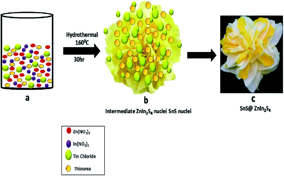
Furthermore, the formation mechanism is schematically depicted in Scheme 1. The hydrothermal reaction conditions are well known to obtain different morphologies. In the present case, the reaction between precursor salt solutions and thiourea confirmed the formation of ZnIn2S4 nuclei under hydrothermal conditions. Thiourea is water-soluble and stable at room temperature, and as the temperature increased, it got decomposed and formed H2S and NH2CN. Then, NH2CN reacted with water at 160 °C and released NH3 and CO2 gas. The overall reaction is shown as follows:34
| Zn(NO3)2 + 2In(NO3)3 + SnCl2 + 10N2H4CS + nH2O → SnS@ZnIn2S4 + 8HNO3 + 18NH3 + 2HCl + 5H2S + 8CO2 |
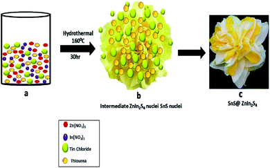 |
| | Scheme 1 Schematic of the formation mechanism of SnS@ZnIn2S4 nano-heterostructures. | |
The Zn2+ In3+ and Sn2+ cations easily get attracted to S2− anions in an aqueous solution of thiourea. Zn(NO3)2 and In(NO3)3 have a very high degree of ionization in the aqueous medium due to its polarity.35 In an aqueous solution of thiourea, the ZnIn2S4 petal grows slowly with prolonged reaction time. The nascent ZnIn2S4 is unstable due to its high surface energy; to reduce these energies, they get aggregated due to the van der Waals force of attraction between small crystallites. Finally, the 2D growth of nanoparticles takes place, which self-assembled to form a hierarchical marigold flower-like structure. The growth of SnS is very slow because of the low concentration of Sn precursors in the reaction. During the hydrothermal reaction, the growth of ZnIn2S4 is fast as compared to SnS. Hence, SnS nanopetals decorated on the surface of ZnIn2S4, which is in good agreement with the FE-TEM images. The above-discussed mechanism is based on our experimental evidence. Such unique twin marigold flower-like nanostructures were reported for the first time.
3.3 Optical and electronic studies
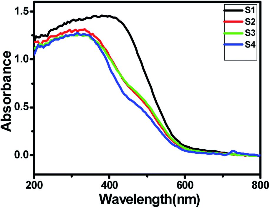
A good solar light absorption capability is a key requirement for highly efficient semiconductor photocatalysts. The absorption properties of pure ZnIn2S4 and SnS@ZnIn2S4 nano-heterostructures were studied by UV-DRS spectra. Fig. 4(a) shows the UV-visible spectrum of ZnIn2S4 and SnS-loaded ZnIn2S4 heterostructures in different molar ratios. The absorption edge of pure ZnIn2S4 is observed to be 600 nm (2.0 eV). The absorption edge of pure SnS is shown in ESI, Fig. III.† The dual band gap is observed for SnS@ZnIn2S4 samples S2–S4.36 Sample S2 and S3 show absorption edges at 610 nm (2.03 eV) and 640 nm (1.7 eV), which correspond to ZnIn2S4 and SnS, respectively. Furthermore, the sample S4 shows an absorption edge at 560 nm (2.21 eV) and 600 nm (2.1 eV), which might be due to ZnIn2S4 and SnS respectively. The reduction in the band gap is an indication of a very intimate interaction between SnS and ZnIn2S4 nanopetals. The first absorption edge found at 516 nm (2.4 eV) is predominant. The increase in band gap clearly reveals the close interaction between ZnIn2S4 flowers and SnS thin sheets. The change in band gap clearly signifies the effect of SnS on ZnIn2S4. As the amount of SnS increases in the composites, the absorption is strongly dominated by SnS present in it. There is a slight shift in the absorption edges to the lower wavelength observed with the increasing SnS concentration; it is due to a lower particle size of the material.
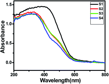 |
| | Fig. 4 UV-DRS spectra of (S1) pure ZnIn2S4, (S2) 1% SnS@ZnIn2S4, (S3) 2% SnS@ZnIn2S4 and (S4) 3% SnS@ZnIn2S4 sample photocatalysts. | |
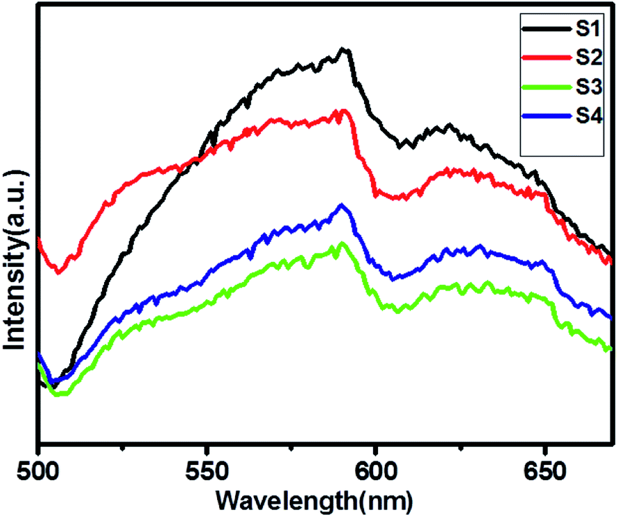
Photoluminescence (PL) spectra is a unique property to evaluate the generation, transfer and separation processes of the photo-induced electrons and hole.37Fig. 5 shows a comparative study of the PL spectra of pure ZnIn2S4 and SnS@ZnIn2S4 excited at a wavelength of 400 nm at room temperature. The PL study of pure SnS is shown in ESI, Fig. IV.† The high PL intensity shows rapid electron–hole pair recombination in a photocatalyst. The pure ZnIn2S4 has strong emission peak at about 590 nm, which is assigned to the origin from the band gap energies transition of ZnIn2S4.38 The PL spectrum of the S2–S4 heterostructure shows the presence of two emission peaks at 530 and 590 nm, which highlights the association of SnS and ZnIn2S4. The PL intensity of SnS@ZnIn2S4 significantly declined with the increase in the content of the SnS sample (S2 and S3), as compared to pure ZnIn2S4. The significant decline in intensity is due to either the faster migration process with the shorter lifetime or the slower recombination process with the longer lifetime for the photo-induced electrons and holes at the interface of two semiconductors as compared to the individual components of the SnS@ZnIn2S4 nano-heterostructure. The incorporation of SnS creates the sulfur vacancy defects, which ultimately reduce the intensity of emission peaks in SnS@ZnIn2S4. Furthermore, high concentrations of SnS (3%) increase the recombination rate due to the shielding of incident light that prevents the generation of electrons inside the ZnIn2S4 nanopetals. Hence, an optimum amount of SnS, i.e. 2% SnS, suppresses the recombination rate. The above-mentioned results reveal that the charge recombination in ZnIn2S4 is effectively suppressed with the increase in the amount of SnS, i.e. due to sulfur vacancy defects.39–41
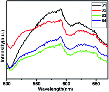 |
| | Fig. 5 UV-DRS spectra of (S1) pure ZnIn2S4, (S2) 1% SnS@ZnIn2S4, (S3) 2% SnS@ZnIn2S4 and (S4) 3% SnS@ZnIn2S4 sample photocatalysts. | |
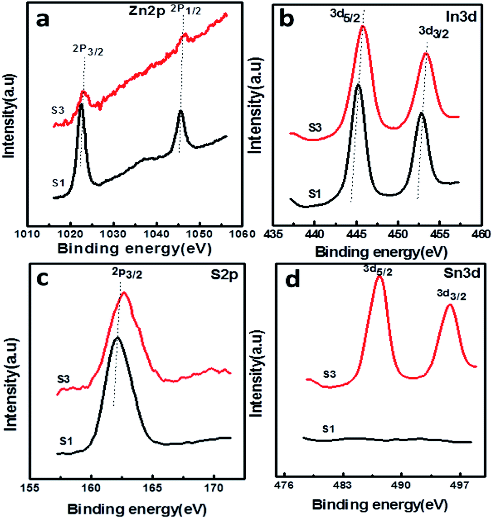
3.4 XPS study
The surface chemical composition and valence state of the SnS@ZnIn2S4 architecture were investigated by X-ray photoelectron spectroscopy. All the peaks were calibrated using the C 1s reference peak at 284.6 eV. Fig. 6(a) shows the XPS signal of Zn 2p observed at binding energies around 1022.3 eV (Zn2+ 2p3/2) and 1045.3 eV (Zn2+ 2p1/2), which is consistent with the results reported in the previous literature.30Fig. 6(b) shows the high-resolution XPS spectra of In 3d at binding energies 444.8 (In3+ 3d5/2) and 452.4 eV (In3+ 3d3/2), which is in good agreement with the previous work.42 Furthermore, the XPS signal (Fig. 6(c)) observed at a binding energy of 161.7 eV is ascribed to the divalent sulfide ions (S2− 2p3/2) which is inconsistent with the data of ZnIn2S4.43Fig. 6(d) shows high-resolution spectra of Sn 3d, where the region can be divided into two different peaks at 487.4 and 497.7 eV. This can be ascribed to the Sn 3d5/2 and Sn3/2 levels of tin in the SnS products, which exist in +2 oxidation state.44 Based on the above-mentioned results, it is evident that SnS nanopetals are overlapped on ZnIn2S4. In comparison with reported binding energies of pure ZnIn2S4, there is a shift in the binding energies of SnS@ZnIn2S4, indicating a strong interaction between ZnIn2S4 and SnS similar to the other reported nano-heterostructures. This close interfacial contact facilitates electron transfer between SnS and ZnIn2S4 to achieve an equivalent position of the Fermi level of both the semiconductors. The optical properties also conclude that the synergic interaction among SnS and ZnIn2S4 matrices exhibits alteration in the electronic band structure of ZnIn2S4 and creates energy levels between C.B and V.B.38
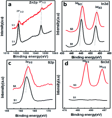 |
| | Fig. 6 XPS spectra of the as-prepared SnS@ZnIn2S4 nanocomposites: (a) Zn 2p, (b) In 3d, (c) S 2p, and (d) Sn 3d. | |
3.5 Photocatalytic study
3.5.1 Photocatalytic activity measurement.
As conferred earlier, SnS@ZnIn2S4 is a good semiconductor having a narrow band gap falling in the visible region at room temperature. Considering the good response towards solar light, photocatalytic activities of SnS@ZnIn2S4 have been investigated. Herein, we report the photocatalytic H2 evolution performance from water and H2S under natural solar light irradiation.
3.5.2 Photocatalytic H2 evolution from H2O and H2S splitting.
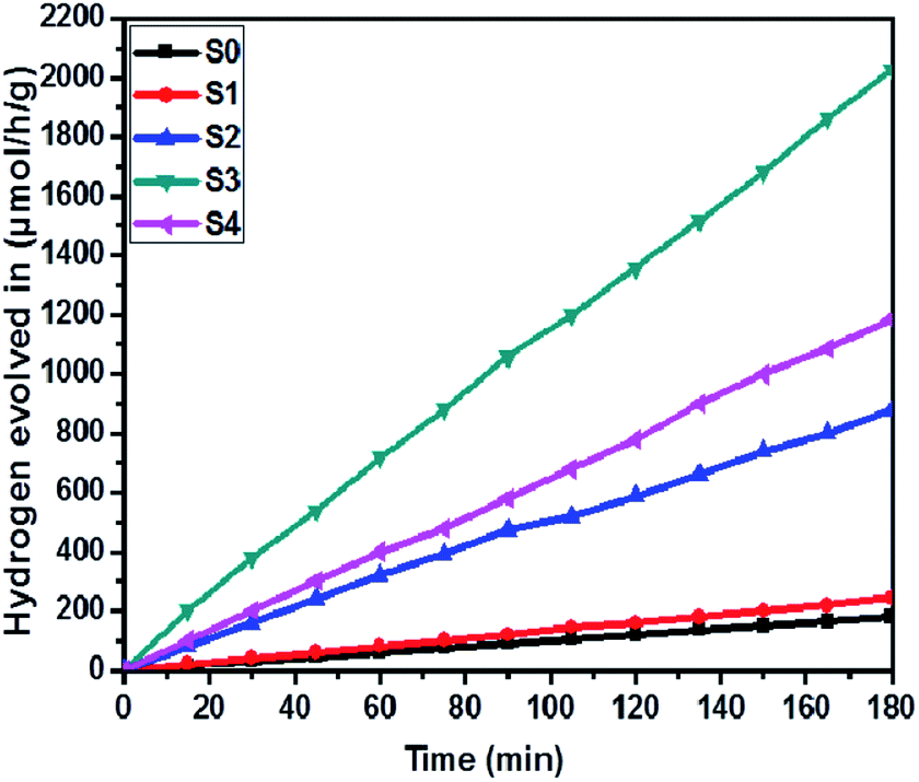
The effect of SnS loading on ZnIn2S4 and their photocatalytic activity of hydrogen generation were studied under solar light irradiation using Na2S/Na2S2O3 as a scavenger electron donor.45 A series of experiments were performed using different concentrations of SnS on the surface of ZnIn2S4, and their results are given in Table 1. The investigation results indicated that the maximum hydrogen generation, i.e. 650 μmol h−1 g−1, was obtained for the sample S3, whereas pure ZnIn2S4, and SnS shows hydrogen evolution rates of 80.2 and 115.5 μmol h−1 g−1. Furthermore, 1% SnS-decorated ZnIn2S4 and 3% SnS-decorated ZnIn2S4 give 386.3 and 290 μmol h−1 g−1 respectively. Fig. 7 shows the time-dependent hydrogen generation using the as-synthesized ZnIn2S4 and SnS@ZnIn2S4 nano-heterostructures. The linearity of the graph shows a continuous and stable hydrogen generation rate. However, the pure ZnIn2S4 shows poor hydrogen evolution, i.e. 115.5 μmol h−1 g−1, whereas maximum hydrogen production, i.e. 650 μmol h−1 g−1, was obtained for sample 2% SnS@ZnIn2S4 (S3) nano-heterostructure, which reveals that most exciting electrons are available for proton reduction. For this experiment, we used 70 mL DI water and Na2S/Na2S2O3 mixture as a sacrificial agent. In the present case, 0.25 M Na2S and 0.35 M Na2S2O3 mixture were used to resist the photo-corrosion of the semiconductor. Moreover, the Na2S solution acts as a hole scavenger, and it oxidized S22− into S2−, which is beneficial for hydrogen generation from SnS@ZnIn2S4 rather than alcohol. The photocatalytic hydrogen generation mechanism from water is well reported and discussed in the previous literature.38 The semiconductor photocatalyst after interaction with solar light with energy greater than or equal to band gap energy generates electrons in CB and holes in VB. It causes redox reactions of adsorbed species on a semiconducting material. The photogenerated holes from VB irreversibly oxidize S22−, which was reduced back to S2− by Na2S2O3 and radially got adsorbed on the surface of semiconductor producing protons (H+) and free radicals, while electrons from CB reduce H+ ions into molecular hydrogen.46| |  | (1) |
| | | Oxidation: SO32− + 2OH− + 2h+ → SO42− + 2H+ | (2) |
| | | : S22− + SO32− → S2O32− + S2− | (4) |
| | | : SO32− + S2− + 2h+ → S2O32− | (5) |
| | | Reduction: H+ + 2e− → H2 | (6) |
Table 1 H2 generation rates for the as-synthesized ZnIn2S4, SnS and SnS@ZnIn2S4 nanocomposites
| Sr. no. |
Sample code |
H2 evolution rate from water (μmol h−1 g−1) |
H2 evolution rate from H2S (μmol h−1 g−1) |
| 1 |
S0 |
80.2 |
3287 |
| 2 |
S1 |
115.5 |
4180 |
| 3 |
S2 |
386.3 |
5593 |
| 4 |
S3 |
650 |
6429 |
| 5 |
S4 |
290 |
5808 |
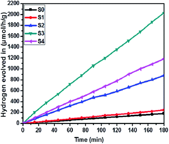 |
| | Fig. 7 Time versus volume of H2 (μmol h−1 g−1) evolution from H2O of all the samples synthesized at 160 °C for 30 h: (S0) pure SnS, (S1) pure ZnIn2S4 and SnS@ZnIn2S4 nano-heterostructures prepared with different percentages of SnS loading: (S2) 1%, (S3) 2% and (S4) 3%. | |
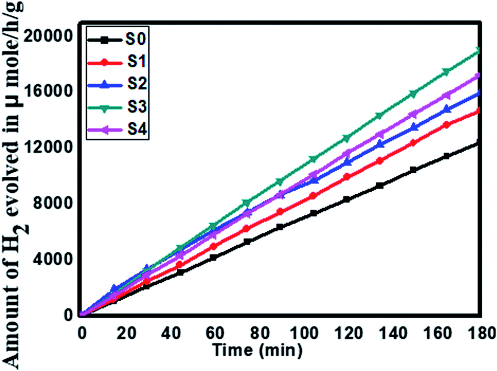
Furthermore, considering the good performance of hydrogen generation from water, we have also performed H2S splitting under solar light irradiation. The photocatalytic hydrogen generation via decomposition of hydrogen sulfide (H2S) was also carried out using the as-synthesized SnS@ZnIn2S4 nano-heterostructure without any sacrificial reagents under solar light. Fig. 8 shows the time-dependent hydrogen generation rate from H2S splitting using the as-synthesized SnS@ZnIn2S4 nanocomposite. The photocatalytic hydrogen generation mechanism from H2S is well reported and discussed in the previous literature.34,35 The pure SnS (S0) and ZnIn2S4 (S1) samples exhibit hydrogen evolution rates of 3287 and 4180 μmol h−1 g−1 respectively, whereas, 1%, 2% and 3% SnS-loaded ZnIn2S4 (S2–S4) samples exhibit hydrogen evolution rates of 5593, 6429 and 5808 μmol h−1 g−1 respectively. From experimental results, it is observed that the loading of SnS on ZnIn2S4 enhances the hydrogen generation efficiency compared with pure SnS and ZnIn2S4. The highest hydrogen generation, i.e. 6429 μmol h−1 g−1, was obtained using the 2% SnS-loaded ZnIn2S4 sample (S2). In both the cases, hydrogen evolution is higher than that reported in earlier studies (Table 2 ESI†).
 |
| | Fig. 8 Time versus volume of H2 (μmol h−1 g−1) evolution from H2S of all the samples synthesized at 160 °C for 30 h: (S0) pure SnS, (S1) pure ZnIn2S4 and SnS@ZnIn2S4 nano-heterostructures prepared with different percentages of SnS loading: (S2) 1%, (S3) 2%, and (S4) 3%. | |
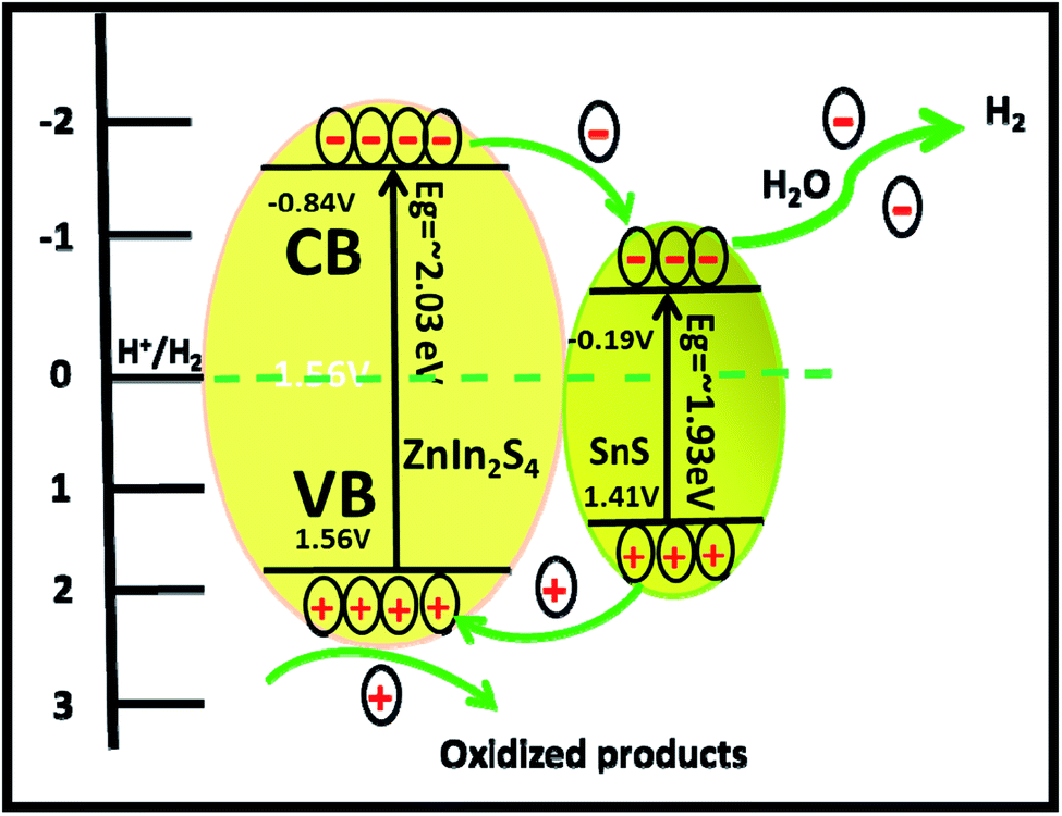
It is exciting to discuss the improved photocatalytic activity in the present case. It is well reported that the photocatalytic activity of semiconductors depends on the adequate band gap, crystallinity, hierarchical morphology, specific surface area, visible light absorption capability, diffusion rate of charge carriers and electronic structure.47 Based on the experimental results, enhanced photocatalytic activity ascribed to the formation of heterostructures can be discussed using probable mechanisms. In the PL study, we observed that the intensity of the emission peaks decreases with the percentage of SnS. As discussed earlier, 2% SnS@ZnIn2S4 (S3) shows minimum intensity as compared to others due to vacancy defects. This supports that the as-synthesized SnS@ZnIn2S4 nanopetals are heterojunctions, which enhance the charge separation efficiency. Hence, the enhanced photocatalytic activity is due to effective charge separation by trapped hole formation in ZnIn2S4 and the transportation of electrons to SnS, i.e. slower the recombination process with longer lifetime for photo-assisted electrons and holes at the interface of two semiconductors compared with pristine ZnIn2S4. Hence, in the present case, the SnS nanoplates loaded on the surface of ZnIn2S4 may act as an optical filter or co-catalyst for charge separation. Based on the experimental results, the band gaps of ZnIn2S4 and SnS are 2.03 and 1.7 eV, respectively. Therefore, both ZnIn2S4 and SnS can be excited and generate charge carriers under solar light irradiation. Furthermore, the band structure of SnS@ZnIn2S4 has a stacked system with a metal-nonmetal bridged heterojunction exhibiting type I band alignment, which may be due to the reorganization of charge carriers at the interlayer region. The type I band alignment specifies that the excited charge carriers are confined to opposite layers, which facilitate the effective separation of electron–hole pairs, resulting in enhanced hydrogen generation.40 Pure ZnIn2S4 shows low photocatalytic activity, but due to a well-matched overlapping band structure and intimate contact between SnS and ZnIn2S4, the photogenerated electrons on the surface of SnS can be easily transferred to the CB of ZnIn2S4. It is because the CB band edge potential of SnS is more negative than ZnIn2S4, which results in the accumulation of more negative charges at the ZnIn2S4 region near the junction. Moreover, the holes on the VB of ZnIn2S4 could be transferred to the VB of SnS through the close contact junction.48 It is because the VB band edge potential of ZnIn2S4 is more positive than that of SnS, which results in a more positive charge accumulated at the SnS region near the interface, which results in the production of an electric field (E) at the interface. The internal electric field migrates at the interface, which promotes the photoinduced charge carriers to participate in hydrogen generation. In other words, ZnIn2S4 can be excited using sunlight, and electron hole-pairs are simultaneously generated. However, the electrons and holes easily recombine without SnS.49 The formation of SnS@ZnIn2S4 has the synergistic effect between ZnIn2S4 and SnS which changes CB and VB of the ZnIn2S4 flower. It suppresses the recombination probability of charge carriers and making them available for photocatalytic activity. It is concluded that the SnS@ZnIn2S4 heterostructure provides electrons and holes to the active sites of the catalyst and reduces the recombination rate. The 2% loading of SnS on ZnIn2S4 suppresses the charge carrier recombination rate significantly.50 Furthermore, the co-existence of sulfur vacancies with optimized concentration can also trap electrons and provide more electrons for hydrogen generation. In addition, the ZnIn2S4 and SnS interface creates a super hydrophilic surface that can effectively improve the contact of semiconductor water, semiconductor H2S, and bubble detachment. The lowering recombination of electron–hole can be correlated by considering the energy level diagram of SnS@ZnIn2S4 heterostructures. The CB of ZnIn2S4 can be shown at −0.84 eV, while VB would be located at 1.56 eV. The Fermi level of SnS −0.19 vs. NHE is more positive than the CB of ZnIn2S4, which indicates that photogenerated electrons can transfer from CB of ZnIn2S4 to SnS (Scheme 2).34,51 Furthermore, with an increase in the concentration of SnS (3% SnS-loaded ZnIn2S4), the photocatalytic activity was found to decrease. It may be due to excessive concentration of SnS (more than 2%), which acts as a recombination center and covers the active sites on ZnIn2S4. Moreover, at a higher concentration of SnS, there is a reduction in charge transfer taking place between SnS and ZnIn2S4, which leads to higher charge recombination. Additionally, the PL study shows a drastic decline in the peak intensity, which also shows suppression in the charge carrier at an optimum concentration of SnS on ZnIn2S4. Furthermore, for 3% of SnS@ZnIn2S4, the PL intensity increases slightly and shows an increase in the charge carrier recombination rate, which may be due to either the faster migration process with a shorter lifetime or the slower recombination process with a longer lifetime. Hence, higher activity is obtained at a moderate concentration of SnS, i.e. 2%. Overall, the SnS@ZnIn2S4 nano-heterostructure photocatalyst was found to be quite stable and active for hydrogen generation under solar light irradiation. A similar trend of hydrogen generation was observed via H2S and water splitting. The H2 production rate by H2S splitting is more as compared to water because of the lower ΔG for H2S splitting. Overall, sample S3 shows good photocatalytic activity under sunlight. To examine the stability of the catalysts, the experiments have been performed reusing the photocatalysts. We obtained a similar activity after reusing the catalysts for 3 cycles (Fig. V and VI ESI†). It shows that the heterostructure is quite stable and can be used for many cycles.
 |
| | Scheme 2 Schematic of the photocatalytic mechanism of SnS@ZnIn2S4 heterostructures. | |
4. Conclusion
In summary, highly efficient 2D SnS@ZnIn2S4 nanoheterostructure flowers have been designed by a hydrothermal method, in which SnS nanopetals decorated in situ on the surface of ZnIn2S4 nanopetals for the first time. An excellent photocatalytic hydrogen evolution rate of 6429 μmol h−1 g−1 was obtained for 2% SnS@ZnIn2S4, under solar light irradiation from H2S, which is 1.6–2 times higher than that of pure ZnIn2S4. At the same time, an excellent photocatalytic hydrogen evolution rate of 650 μmol h−1 g−1 was obtained by water splitting, which is 6 times higher than that of bare ZnIn2S4. The enhanced photocatalytic activity of the SnS@ZnIn2S4 photocatalyst was ascribed to efficient charge separation and transportation of the photogenerated electron–hole pairs through the formation of “type I band alignment” at the interface and increase in the visible light response. More significantly, the hierarchical nanostructure of SnS@ZnIn2S4 enhances the photocatalytic activity due to the efficient charge carrier separation, which has been examined using the PL study. It also reveals a moderate amount of SnS incorporation that gives good photocatalytic activity. The reusability of the photocatalyst exhibits similar activities, which reveals the good stability of the catalyst.
Conflicts of interest
There are no conflicts to declare.
Acknowledgements
ARG and AKK would like to thanks Dr R. J. Barnabas (Principal Ahmednagar College Ahmednagar) for useful discussion and ASPIRE SPPU for financial support. The authors would like to thank Nanocrystalline Materials Group, C-MET, Pune and Ahmednagar College Ahmednagar, for the kind support. Dr Jin-Ook Baeg thanks to KRICT for support. BBK would like to thank the Ministry of Electronics and Information Technology (MeitY), Government of India for financial support and C-MET Pune for providing research facilities. ARG would like to acknowledge to SPPU Pune for Providing J. R. D. Tata fellowship for Research work.
References
- F. E. Osterloh, Chem. Mater., 2008, 20, 35–54 CrossRef CAS.
- J. Zheng, H. Zhou, Y. Zou, R. Wang, Y. Lyu, S. P. Jiang and S. Wang, Energy Environ. Sci., 2019, 12, 2345–2374 RSC.
- I. Staffell, D. Scamman, A. Velazquez Abad, P. Balcombe, P. E. Dodds, P. Ekins, N. Shah and K. R. Ward, Energy Environ. Sci., 2019, 12, 463–491 RSC.
- A. K. Kulkarni, R. P. Panmand, Y. A. Sethi, S. R. Kadam, S. P. Tekale, G. H. Baeg, A. V. Ghule and B. B. Kale, Int. J. Hydrogen Energy, 2018, 43, 19873–19884 CrossRef CAS.
- A. Kudo and Y. Miseki, Chem. Soc. Rev., 2009, 38, 253–278 RSC.
- X. Chen, S. Shen, L. Guo and S. S. Mao, Chem. Rev., 2010, 110, 6503–6570 CrossRef CAS PubMed.
- R. K. Chava, J. Y. Do and M. Kang, J. Mater. Chem. A, 2019, 7, 13614–13628 RSC.
- Z. Wang, C. Li and K. Domen, Chem. Soc. Rev., 2019, 48, 2109–2125 RSC.
- Z. Wang, J. Peng, X. Feng, Z. Ding and Z. Li, Catal. Sci. Technol., 2017, 7, 2524–2530 RSC.
- T. Hisatomi, J. Kubota and K. Domen, Chem. Soc. Rev., 2014, 43, 7520–7535 RSC.
- A. Fujishima and K. Honda, Nature, 1972, 238, 37–38 CrossRef CAS PubMed.
- H. Luo, W. Song, P. G. Hoertz, K. Hanson, R. Ghosh, S. Rangan, M. K. Brennaman, J. J. Concepcion, R. A. Binstead, R. A. Bartynski, R. Lopez and T. J. Meyer, Chem. Mater., 2013, 25, 122–131 CrossRef CAS.
- S. P. Adhikari, Z. D. Hood, K. L. More, I. Ivanov, L. Zhang, M. Gross and A. Lachgar, RSC Adv., 2015, 5, 54998–55005 RSC.
- X. Sun, Q. Li, J. Jiang and Y. Mao, Nanoscale, 2014, 6, 8769–8780 RSC.
- M. Sathish, B. Viswanathan, R. P. Viswanath and C. S. Gopinath, Chem. Mater., 2005, 17, 6349–6353 CrossRef CAS.
- P. A. Bharad, K. Sivaranjani and C. S. Gopinath, Nanoscale, 2015, 7, 11206–11215 RSC.
-
(a) S. Mandala, S. Adhikari, P. Shengyana, M. Huia and D. M. Kim, Appl. Surf. Sci., 2019, 498, 143840 CrossRef;
(b) X. Liu, J. Iocozzia, Y. Wang, X. Cui, Y. Chen, S. Zhao, Z. Li and Z. Lin, Energy Environ. Sci., 2017, 10, 402–434 RSC.
- X. Zhang, Z. Lai, Q. Ma and H. Zhang, Chem. Soc. Rev., 2018, 47, 3301–3338 RSC.
- M. Faraji, M. Yousefi, S. Yousefzadeh, M. Zirak, N. Naseri, T. H. Jeon, W. Choi and A. Z. Moshfegh, Energy Environ. Sci., 2019, 12, 59–95 RSC.
- B. B. Kale, J.-O. Baeg, S. K. Apte, R. S. Sonawane, S. D. Naik and K. R. Patil, J. Mater. Chem., 2007, 17, 4297–4303 RSC.
- D. Voiry, M. Salehi, R. Silva, T. Fujita, M. Chen, T. Asefa, V. B. Shenoy, G. Eda and M. Chhowalla, Nano Lett., 2013, 13, 6222–6227 CrossRef CAS PubMed.
- B. Chai, T. Peng, P. Zeng and J. Mao, J. Mater. Chem., 2011, 21, 14587–14593 RSC.
- Y. Hong, J. Zhang, F. Huang, J. Zhang, X. Wang, Z. Wu, Z. Lin and J. Yu, J. Mater. Chem. A, 2015, 3, 13913–13919 RSC.
- A. F. Shaikh, S. S. Arbuj, M. S. Tamboli, S. D. Naik, S. B. Rane and B. B. Kale, ChemistrySelect, 2017, 2, 9174–9180 CrossRef CAS.
- B. B. Kale, J.-O. Baeg, S. M. Lee, H. Chang, S.-J. Moon and C. W. Lee, Adv. Funct. Mater., 2006, 16, 1349–1354 CrossRef CAS.
- S. Shen, L. Zhao and L. Guo, Int. J. Hydrogen Energy, 2008, 33, 4501–4510 CrossRef CAS.
- S. R. Kadam, D. J. Late, R. P. Panmand, M. V. Kulkarni, L. K. Nikam, S. W. Gosavi, C. J. Park and B. B. Kale, J. Mater. Chem. A, 2015, 3, 21233–21243 RSC.
-
(a) J. Pan, Z. Guan, J. Yang and Q. Li, Chin. J. Catal., 2020, 41, 200–208 CrossRef CAS;
(b) N. S. Chaudhari, A. P. Bhirud, R. S. Sonawane, L. K. Nikam, S. S. Warule, V. H. Rane and B. B. Kale, Green Chem., 2011, 13, 2500–2506 RSC.
- G. Yang, D. Chen, H. Ding, J. Feng, J. Z. Zhang, Y. Zhu, S. Hamid and D. W. Bahnemann, Appl. Catal., B, 2017, 219, 611–618 CrossRef CAS.
- J. Hou, C. Yang, H. Cheng, Z. Wang, S. Jiao and H. Zhu, Phys. Chem. Chem. Phys., 2013, 15, 15660–15668 RSC.
- Y. Chen, G. Tian, W. Zhou, Y. Xiao, J. Wang, X. Zhang and H. Fu, Nanoscale, 2017, 9, 5912–5921 RSC.
- F. Fang, L. Chen, Y.-B. Chen and L.-M. Wu, J. Phys. Chem. C, 2010, 114, 2393–2397 CrossRef CAS.
- L. Wang, H. Zhai, G. Jin, X. Li, C. Dong, H. Zhang, B. Yang, H. Xie and H. Sun, Phys. Chem. Chem. Phys., 2017, 19, 16576–16585 RSC.
- S. B. Kale, R. S. Kalubarme, M. A. Mahadadalkar, H. S. Jadhav, A. P. Bhirud, J. D. Ambekar, C.-J. Park and B. B. Kale, Phys. Chem. Chem. Phys., 2015, 17, 31850–31861 RSC.
- N. S. Chaudhari, S. S. Warule and B. B. Kale, RSC Adv., 2014, 4, 12182–12187 RSC.
- M. A. Mahadik, P. S. Shinde, M. Cho and J. S. Jang, J. Mater. Chem. A, 2015, 3, 23597–23606 RSC.
-
(a) Z. Guan, J. Pan, Q. Li, G. Li and J. Yang, ACS Sustainable Chem. Eng., 2019, 7, 7736–7742 CrossRef CAS;
(b) A. K. Kulkarni, Y. A. Sethi, R. P. Panmand, L. K. Nikam, J.-O. Baeg, N. R. Munirathnam, A. V. Ghule and B. B. Kale, J. Energy Chem., 2017, 26, 433–439 CrossRef.
- W. Y. Lim, M. Hong and G. W. Ho, Dalton Trans., 2016, 45, 552–560 RSC.
- X. Gao, J. Wang, J. Yu and H. Xu, CrystEngComm, 2015, 17, 6328–6337 RSC.
- M. A. Mahadadalkar, S. W. Gosavi and B. B. Kale, J. Mater. Chem. A, 2018, 6, 16064–16073 RSC.
-
B. Ghosh, M. Das, P. Banerjee and S. Das, Fabrication and optical properties of SnS thin films by SILAR method, 2008 Search PubMed.
- L. Ye, J. Fu, Z. Xu, R. Yuan and Z. Li, ACS Appl. Mater. Interfaces, 2014, 6, 3483–3490 CrossRef CAS PubMed.
- H. Jia, W. He, Y. Lei, X. Chen, Y. Xiang, S. Zhang, W. M. Lau and Z. Zheng, RSC Adv., 2013, 3, 8909–8914 RSC.
- B. Subramanian, C. Sanjeeviraja and M. Jayachandran, Mater. Chem. Phys., 2001, 71, 40–46 CrossRef CAS.
- P. Gomathisankar, K. Hachisuka, H. Katsumata, T. Suzuki, K. Funasaka and S. Kaneco, ACS Sustainable Chem. Eng., 2013, 1, 982–988 CrossRef CAS.
- S. R. Lingampalli, U. K. Gautam and C. N. R. Rao, Energy Environ. Sci., 2013, 6, 3589–3594 RSC.
- Y. A. Sethi, C. S. Praveen, R. P. Panmand, A. Ambalkar, A. K. Kulkarni, S. W. Gosavi, M. V. Kulkarni and B. B. Kale, Catal. Sci. Technol., 2018, 8, 2909–2919 RSC.
-
(a) S. Adhikari, A. V. Charanpahari and G. Madras, ACS Omega, 2017, 2, 6926–6938 CrossRef CAS PubMed;
(b) S. Wang, B. Y. Guan, X. Wang and X. W. D. Lou, J. Am. Chem. Soc., 2018, 140, 15145–15148 CrossRef CAS PubMed.
- H. Wang, H. Ye, B. Zhang, F. Zhao and B. Zeng, J. Phys. Chem. C, 2018, 122, 20329–20336 CrossRef CAS.
- S. Shen, X. Chen, F. Ren, C. X. Kronawitter, S. S. Mao and L. Guo, Nanoscale Res. Lett., 2011, 6, 290 CrossRef PubMed.
- S. Jayswal and R. S. Moirangthem, New J. Chem., 2018, 42, 13689–13701 RSC.
Footnote |
| † Electronic supplementary information (ESI) available. See DOI: 10.1039/d0na00175a |
|
| This journal is © The Royal Society of Chemistry 2020 |
Click here to see how this site uses Cookies. View our privacy policy here. 
 Open Access Article
 This Open Access Article is licensed under a Creative Commons Attribution-Non Commercial 3.0 Unported Licence
 a,
Jin
Ook-Baeg
a,
Jin
Ook-Baeg