DOI:
10.1039/D0NA00139B
(Paper)
Nanoscale Adv., 2020,
2, 3350-3357
A solar-responsive zinc oxide photoanode for solar-photon-harvester photoelectrochemical (PEC) cells†
Received
19th February 2020
, Accepted 8th June 2020
First published on 8th June 2020
Abstract
A highly efficient, nanostructured, solar-responsive zinc-oxide (SRZO) photoanode has been achieved by utilization of a versatile solution precursor plasma spray (SPPS) deposition technique. For the first time, it is demonstrated that a front-illumination type SRZO photo-anode fabricated with a ZnO/stainless steel (SS-304) configuration can generate an enhanced photo-electrochemical (PEC) current of 390 μA cm−2, under solar radiation from a solar simulator with an AM1.5 global filter (∼1 sun). The SRZO electrode displayed a solar-to-hydrogen (STH) conversion efficiency of 2.32% when investigated for H2 evolution in a PEC cell. These electrodes exhibited a maximum peak efficiency of 86% using 320 nm photons during incident photon-to-current conversion efficiency measurement. Interestingly, the film lattice of SRZO showed a significant red-shift of 0.37 eV in the ZnO band gap thereby providing solar photon absorptivity to SRZO. Further, an enhanced charge transport property by virtue of increased donor density (∼4.11 × 1017 cm−3) has been observed, which is higher by an order of magnitude than that of its bulk counterpart. Efficient optical absorption of solar photons and higher donor-density of SRZO have been thus attributed to its superior PEC performance.
1. Introduction
Tuning the opto-electronic properties by utilization of nano-structuring is highly desirable, and key to performance improvement in solar-cells and photo-electrochemical (PEC) devices. Since the first report on PEC application of TiO2, it is always seen that TiO2 suffers from its UV absorbing property which makes it unsuitable as a visible light active material.1 A similar obstacle has also been faced by most other wide band gap semiconducting metal-oxides such as SrTiO3, ZnO etc. This necessitates one to architecture a new visible light active material that will not only fulfil the shortcomings of TiO2 or ZnO for energy applications, but would also be useful as an attractive renewable energy generating material. Fabrication of a visible light active material can be achieved by band gap engineering via metal-ion doping, composite formation, hetero-junction formation, size/shape dependent nano-structuring etc.2–21 The research community worldwide has been largely utilizing expensive and complex materials such as ternary and quaternary metal-oxide systems to obtain an energy efficient and stable material.2,3,14,15,19 However, the complexness of the material system and the associated processing methodologies introduce various challenges, thereby inhibiting the commercial viability of the product. In recognition of the above, in order to explore such an opto-electronic property tunability in simple materials, a special effort has been made in this work, employing a novel yet simple approach.
In the present work, we have explored the well-known UV-active ZnO – an economical and eco-friendly photocatalyst, and attempted to achieve a solar-responsive zinc-oxide (SRZO) film by making use of its film thickness dependent optical property tunability. Such SRZO films are highly desirable for PEC water-splitting. ZnO is known to be one of the most efficient and stable UV-active photocatalysts useful for water-splitting and pollutant-remediation in its particulate form as well as in the PEC cell configuration.22–28 However, its solar photocatalytic activity and PEC applicability have suffered due to its wide band gap (Eg ∼ 3.2 eV). This demands enhancing the photon–lattice interaction in ZnO films, which can potentially be realized via various strategies, such as control of film-surface/structure design, surface state density or by interface engineering. Accomplishing the above can provide optical property tunability as required in solar absorbing PEC cells. Accordingly, it is possible to explore an appropriate option to realize the above concept by optical/electronic property modification by nano-patterning, planar nano-cavities, structural stress induced band-gap reduction etc.29–34 Such efforts can be a promising pathway to overcome the limitations of low-absorption of a low/wide band gap semiconductor and yield an improved photoactive energy material. In the present context, the band-gap reduction acquired by complex optical processes induced at the interface and surface state effects are of prime interest but challenging to achieve. This paper details our attempt to modulate the complex interface related optical processes occurring at the interface of ZnO over-layers on a stainless steel substrate, to attain an efficient visible light active ZnO-based photoelectrode.
We have successfully fabricated SRZO photoanodes for PEC cells. We have also for the first time shown a very high photocurrent generation in a front-illumination type PEC cell configuration, which yields the added advantage of excluding the necessity of an optically transparent base electrode. This has been achieved without the loss of photon to energy conversion efficiency. The SRZO photoanode shows dramatically upgraded photocurrent generation during PEC water-splitting, even under solar radiation photons, which otherwise cannot be expected in the case of ZnO photocatalysts due to their wide band gap.
2. Experimental
2.1 Materials
Zinc nitrate (Zn (NO3)2·6H2O with purity 96–103%) was purchased from Merck. Sodium hydroxide pellets (NaOH with 97% purity) were obtained from Fisher Scientific. A saturated calomel electrode (SCE) was purchased from Princeton Applied Research Laboratories.
2.2 SRZO film deposition
In order to fabricate SRZO photoanodes, ZnO films of various thicknesses were deposited by the SPPS technique using a procedure similar to that reported earlier for the case of spinel ZnFe2O4.35 Briefly, an aqueous solution of Zn(NO3)2, with the precursor concentration ranging from 0.1 to 0.5 M metal precursor, was used for the deposition of ZnO films over different substrates (steel, Al2O3, glass, quartz etc.). ZnO films deposited on stainless steel (SS-304) substrates have been described in the present report. These substrates were cleaned and roughened by grit blasting prior to film deposition. Thus cleaned, and plasma spray gun preheated (400 °C) substrates were used for solution precursor plasma spray (SPPS) film deposition (see Fig. S1, ESI†). A complete optimization of spray parameters was carried out to deposit efficient films. The optimization was done on the basis of film PEC performance. In the present study, we used films of various thicknesses named (A) 5.0; (B) 8.0; (C) 12.0; (D) 25.0 μm and (E) 100 μm as shown in Table 1. In order to carry out the film deposition using the solution precursor plasma spray technique, a robotic DC 9MB plasma spray system (Sulzer Metco AG, Switzerland) attached with an SPS-II liquid delivery unit (Inframat Corporation, USA) was used as described in our earlier report.35 It may be added that in the present case the film thickness variation was achieved via changing the number of sprays during the SPPS deposition as described in our past reports.
Table 1 Different properties of ZnO films of different thicknessesa
| Film |
Thickness (μm) |
Crystallite size (nm) |
Optical band gap (eV) |
Photocurrent density (μA cm−2) |
STH conversion efficiency (%) |
IPCEb (%) |
Flat band potential V w.r.t NHE |
Donor density × 1017/cm−3 |
Depletion width (nm) |
|
Film E shows a band gap of 3.2 eV similar to bulk ZnO but shows no photocurrent under simulated (AM 1.5G) solar radiation.
IPCE at 320 nm wavelength.
|
| A |
5.0 |
11 |
2.9 |
188 |
0.10 |
50 |
−0.499 |
0.24 |
22.13 |
| B |
8.0 |
16 |
2.8 |
390 |
2.32 |
86 |
−0.527 |
4.11 |
53.48 |
| C |
12.0 |
17 |
2.9 |
306 |
0.92 |
41 |
−0.486 |
9.27 |
35.61 |
| D |
25.0 |
19 |
3.0 |
14 |
0.38 |
5 |
−0.668 |
6.19 |
43.59 |
2.3 Structural, optical and morphological characterization
Understanding the physico-chemical properties of films is key to achieving efficient performance of the photoanode. Structural studies of the as-prepared ZnO films were carried out using an advanced X-ray diffraction (XRD) system (Bruker AXS D8), equipped with a Lynx eye detector, and CuKα radiation was used to ascertain the phase constitution of the films. The film morphology and cross-section were studied using a field-emission scanning electron microscope (Hitachi S4300SE/N). The film microstructure was further characterized by transmission electron microscopy (TEM) using a Tecnai 210 TEM working at 200 kV, equipped with an energy dispersive X-ray spectroscopy (EDS) system. The optical properties of the films were investigated using a UV-Vis spectrophotometer (Carey 5000 model).
2.4 PEC measurement, PEC cell fabrication and H2 evolution detection
Photoelectrochemical measurements were carried out in a specially designed and fabricated closed gas PEC reactor cell with a quartz window that can be used to irradiate the photoanode under a solar simulator (vertical illumination). A unit area (1 cm2) of SRZO film immersed in sodium hydroxide (0.5 M) was used as the working electrode and a graphitic surface as the counter electrode. The reactor was also useable to estimate hydrogen evolution during PEC experiments. The rate of H2 evolution was detected using a gas chromatograph (Shimadzu 2010AFT) equipped with a thermal conductivity detector. For the hydrogen evolution study, the volume of the evolved hydrogen gas was estimated for a specific irradiation time. There was no evolution of gas when the illumination was “OFF”. A saturated calomel electrode (SCE) was used as the reference electrode for all the electrochemical measurements reported here, unless otherwise stated. A potentiostat/FRD (PARSTAT 2273, Princeton Applied Research) was employed to apply external electrical biasing and to record the time dependent photocurrent generation from SRZO. A Xe-lamp (300 W) containing a solar simulator (Newport) equipped with an AM1.5 global filter was used as an illumination source during the PEC measurement. Similarly, for incident-photon-current conversion efficiency (IPCE) measurements, a Xe-lamp (300 W) fitted with a monochromator (Oriel Newport 74125 model) was used to evaluate the wavelength-dependent performance of all the photoanodes studied. For this, the spectra were recorded in the wavelength range of 250 nm to 700 nm at a wavelength interval of 10 nm. Mott–Schottky (MS) measurements were carried out with a built-in frequency response detector (Model-1025) of the PARSTAT-2273 potentiostat.
3. Results
SRZO photoanodes were fabricated using the SPPS deposition technique. The film PEC performance was considered to optimize the spray parameters to obtain efficient films. In the present study, we used films of certain thicknesses (5–100 μm), as shown in Table 1. While films A–D were within the desired thickness range for SRZO photoanode applications and characterized in detail, film E (100 μm thick film) was used as the reference for comparison as it showed a band gap of ∼3.2 eV similar to bulk ZnO.
Fig. 1(a) shows the X-ray diffraction spectra of the ZnO films, A–D, deposited using the SPPS technique. The spectra confirm the formation of a hexagonal ZnO structure with the P63mc space group (JCPDS 00-036-1451). It is clearly evident that the intensity of reflection from all peaks especially hkl of 100, 002 and 101 increased, with the thickness increasing from A–D. This implied that there is a progressive increase in ZnO crystallinity with an increase in the film thickness. A detailed spectral analysis indicated that the calculated lattice parameters, a = 3.24982 Å and c = 5.20661 Å, match well with those of bulk ZnO.34 The substrate peaks due to SS-304 persisted in all the films except D. It clearly showed that the peak intensity due to the substrate synchronously decreased from film A to D. There was no detectable impurity peak (such as iron oxide etc.) within the limits of XRD. Furthermore, in each case, the crystallite size as estimated from the Debye–Scherrer formula was found to lie in the range of 11–19 nm, as presented in Table 1.36 This indicates that the films are composed of nanocrystals of ZnO.
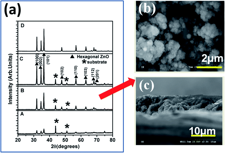 |
| | Fig. 1 (a) XRD spectra of ZnO films of different thicknesses; (b) morphology and (c) cross-section of film B. | |
Fig. 1(b) and (c) display the FESEM images of the film surface and the corresponding film cross-section, respectively, for a typical sample of film B. The film surface was found to consist of nano-clusters comprising smaller than 20 nm nanocrystals (as also confirmed from the XRD) over the entire electrode area, thus revealing its nanoscopic nature. The film surface is also suggestive of the porous nature of the film which is expected to enhance its specific surface area. The film cross-section clearly validates that the film growth occurred via nano-particulate entities with respect to the increase in the film thickness. The cross-sectional view demonstrates that the thickness of film B is ∼8 μm. It is pertinent to mention that there was no distinct difference in the film morphologies of other films (A, C, and D) (see Fig. S2, ESI†), and they were found to be analogous to film B, and further contained nanoparticulates. Formation of such a film surface morphology is a salient feature of the SPPS deposition technique. The estimated film thickness values of the coatings are summarized in Table 1, which clearly demonstrates the control of film thickness achieved by optimization of deposition parameters. In each case, the formation of nanoscopic films over SS using SPPS is apparent and single phase high crystallinity ZnO films have been achieved for all thicknesses.
The film structure and morphology were further confirmed from TEM studies as shown in Fig. 2. Fig. 2(a) shows the morphology of film B which demonstrates that the film consists of nano-dimensional crystallites of size <20 nm which is in agreement with the crystallite size estimated using the Debye–Scherrer formula from XRD. Further, a detailed analysis of the selected area electron diffraction (SAED) pattern recorded for the film confirms the existence of all the planes of ZnO that were observed in XRD.
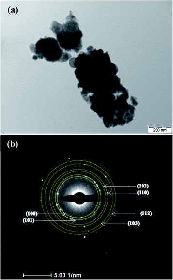 |
| | Fig. 2 (a) TEM morphology and (b) selected area electron diffraction (SAED) pattern of film B. | |
The optical properties of the as-deposited ZnO films were investigated using diffuse reflectance measurements. Fig. 3 shows the comparison of the diffuse reflectance spectra of films A to E and reveals the influence of the increase in film thickness. Interestingly, all the films (except E) showed enhanced light absorption in the visible range. Thus, they are termed solar-responsive zinc-oxide films. Further, observation of band-edge values indicates that film-A exhibits a maximum red-shift, which decreases systematically up to film-D, and finally film-E exhibited absorption in the UV region and showed a band gap of 3.2 eV which is similar to the bulk ZnO value. To understand this, we carried out a detailed Tauc analysis of these spectra (see Fig. S3, ESI†) and estimated the respective direct band gap of the films.37 The inset in Fig. 3 shows the variation of band gap with films as calculated using Tauc analysis. The optical data of these films fitted well for the direct transitions as expected. Film-B showed the lowest band-gap of 2.8 eV indicating a maximum red-shift of 0.33 eV with respect to the bulk ZnO band gap of 3.2 eV. It can be clearly observed that this red-shift in the band gap is achieved by favorable effects of optical scattering occurring due to the depth of the nanoparticulate film, and the interaction of the incident photons at the film/substrate interface. Additionally, it is noteworthy that layers comprising nano-particulates are expected to exhibit surface induced effects and modulate the band-gap transitions in such systems.38 Thus, the optical studies clearly validate that the red-shifted band gap provides visible light absorptivity to the wide band gap ZnO semiconductor. Hence, this demonstrates an achievement of SRZO for potential PEC applications.
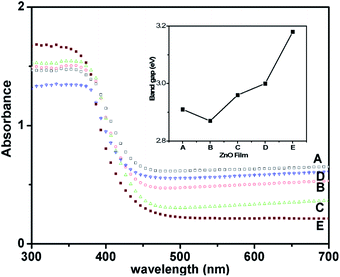 |
| | Fig. 3 Diffuse reflectance spectra of ZnO films. Film-E has been included as the reference. The inset shows the energy band gap of different films estimated from Tauc analysis of respective films. | |
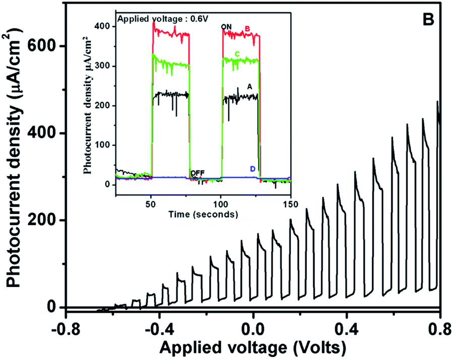
Fig. 4 shows the photocurrent–potential curve for film-B, under chopped light illumination from the solar simulator, indicating the maximum photocurrent (390 μA cm−2) ever reported under solar radiation. Analogously, a very high photocurrent of >5.3 mA cm−2 was observed under white light radiation (see Fig. S4, ESI†). The values of photocurrent densities for SRZO photoanodes are tabulated in Table 1. The inset of Fig. 4 shows the chronoamperometric curves for the fabricated SRZO photoanodes, indicating the maximum photocurrent density for film-B under an applied bias of 0.6 V. Interestingly, the SRZO photoanode fabricated using film-B displayed the highest photocurrent generation among all the photoanodes. Surprisingly, film-B also showed a minimum band gap for SRZO, indicating its ability to harvest larger proportion of solar photons, thereby yielding the most efficient SRZO photoanode. A closer look at the trend in the variation of photocurrents as seen from the inset of Fig. 4 reveals that the SRZO can be arranged in the decreasing order of photocurrent density as Ifilm-B > Ifilm-C > Ifilm-A > Ifilm-D. Thus, we have clearly demonstrated the fabrication of high efficiency SRZO photoanodes. A comparison of PEC performance of film-B with existing reports is presented in Table 2. It clearly shows that SRZO, a nanostructured film deposited by a simple scalable technique, yields an efficient PEC electrode, indicating the advantage of the existing work. Wolcott et al.5 reported glancing angle pulsed laser deposition of ZnO nanoparticle assemblies, which showed a photocurrent density of 142 μA cm−2, which is 2.7 times less than that of the present report. In the case of a special category (nanostructures/nanorods) type electrode, Yao et al. reported a photocurrent density of 1.72 mA cm−2 for hydrogenated ZnO nanorod arrays obtained from annealed films of electrochemically deposited ZnO. The hydrogenated nanorod arrays were obtained by annealing them, first in air and then in a hydrogen atmosphere at 350 °C, resulting in a high photocurrent generated at an applied voltage of 1.23 V vs. RHE.39 The main point of difference here is that the film is hydrogenated and not pure ZnO, and thus it may not be a comparable candidate, though included in Table 2. In another report, Desai et al. discussed about a high photocurrent density of 620 μA cm−2 at 1.23 RHE of a complex nanorod decorated superstructure, which was deposited using a seed layer technique.29 Similarly, Huang et al. reported a photocurrent density of 320 μA cm−2 generated by anodized ZnO nanostructures.40 The comparison in Table 2 clearly shows that SRZO films, which were obtained by a single step deposition technique, generated the highest photocurrent. Additionally, the present work shows the photocurrent generated at the lowest biasing voltage of 0.6 V vs. SCE. Further, actual PEC hydrogen evolution under solar light has not been reported so far, to the best of our knowledge.
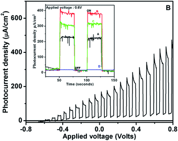 |
| | Fig. 4 Photocurrent–voltage curve of the film-B SRZO photoanode with chopped light illumination under a solar simulator (AM1.5G). The inset shows the comparison of the current transient with time for different SRZO photoanodes under on/off illumination. | |
Table 2 Comparison of PEC photocurrent generated by various ZnO films under solar light as reported in the literaturea
| ZnO electrode type |
Method of preparation |
Photocurrent generated (μA cm−2) at biasing V |
Reference |
|
*Solution precursor plasma spray, light source of solar simulated radiation; **ED – electrochemical deposition; biasing voltage of present work – 600SCE = 850RHE = 650 mV Ag/AgCl.
|
| Normal type |
| Film |
*SPPS |
*390 (at 0.6 V SCE) |
Present work |
| Film |
Pulsed laser deposition |
142 (1 V Ag/AgCl) |
5
|
![[thin space (1/6-em)]](https://www.rsc.org/images/entities/char_2009.gif) |
| Special type |
| Nanorod arrays hydrogenated-ZnO |
**ED + annealing |
1.7 × 10³ (1.23 V RHE) |
39
|
| Nanorod decorated nanosheet |
Seed layer + hydrothermal |
620 (1.23 V RHE) |
29
|
| Nanostructures |
Anodic deposition |
320 (at 0.6 V SCE) |
40
|
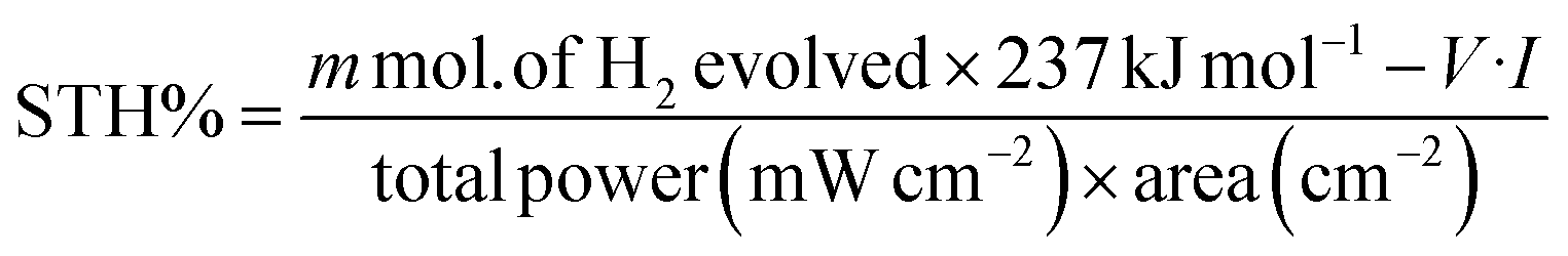
To further investigate the wavelength dependent conversion efficiency of the SRZO photoanodes, incident-photon-current-conversion efficiency (IPCE) measurements were carried out in the wavelength range of 200–700 nm at an interval of 10 nm. The IPCE was estimated and plotted against the incident wavelength. Fig. 5 shows the IPCE spectra of SRZO photoanodes indicating their efficient nature in a front-illumination type PEC cell configuration. It is clear from the figure that film-B shows the maximum conversion efficiency of 86% at 320 nm wavelength compared to other SRZO films. This is in direct correlation with earlier results of SRZO photoanodes with respect to their optical and PEC response. The optical absorption of film B is also shown to correlate both the results. Specifically, the red-shifted absorbance of film B and the major contribution to the IPCE of film B are from larger wavelength photons in the 400–450 nm range compared to other films. Further, the hydrogen evolution capability of these photoanodes under solar light was investigated using PEC at an applied bias voltage of 0.6 V vs. SCE. The evolved hydrogen was detected and quantified using a gas chromatogram. The solar-to-hydrogen conversion efficiency of each photoanode was estimated using the below formula.41
| |  | (1) |
where
V is the applied bias and
I is the obtained photocurrent density. Film B showed a maximum STH efficiency of 2.32% which was significantly higher than that of others. The efficiencies in the case of all the films are well in accordance with other results such as IPCE efficiency, PEC currents and optical absorption recorded for each film. In order to understand the electrochemical behaviour of SRZO photoanodes, their electrochemical characterization was carried out.
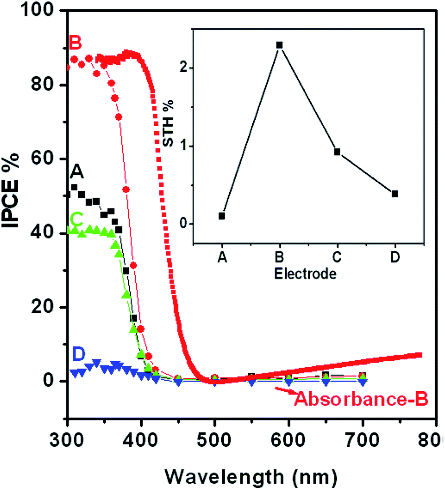
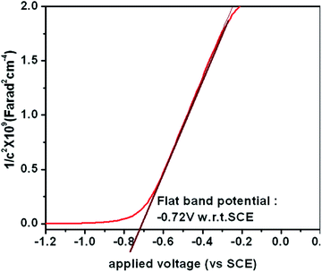
Fig. 6 shows the Mott–Schottky (MS) plot of the most efficient SRZO photoanode fabricated from film-B. Film-B behaves like an n- type semiconductor as evident from the positive slope of the MS-curve. The estimated flat band potential was found to be 0.72 eV in accordance with known reports pertaining to ZnO.
42 The electrochemical characterization is very useful to understand the transport properties of PEC anodes. The donor density and depletion width of the SRZO photoanodes obtained from the above characterization (see Fig. S5, ESI
†) are summarized in
Table 1. The values indicate the favourable differences which facilitate PEC performance improvement.
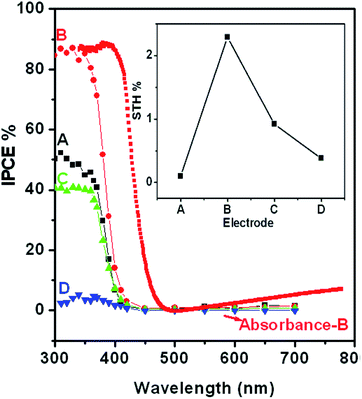 |
| | Fig. 5 Incident-photon-current-conversion efficiency (IPCE) of the ZnO films of different thicknesses in the wavelength range of 300–700 nm. Absorbance of film-B is also shown for correlation. The inset shows the solar-to-hydrogen conversion efficiency of the films A–D. | |
 |
| | Fig. 6 Mott–Schottky plot of film B. | |
4. Discussion
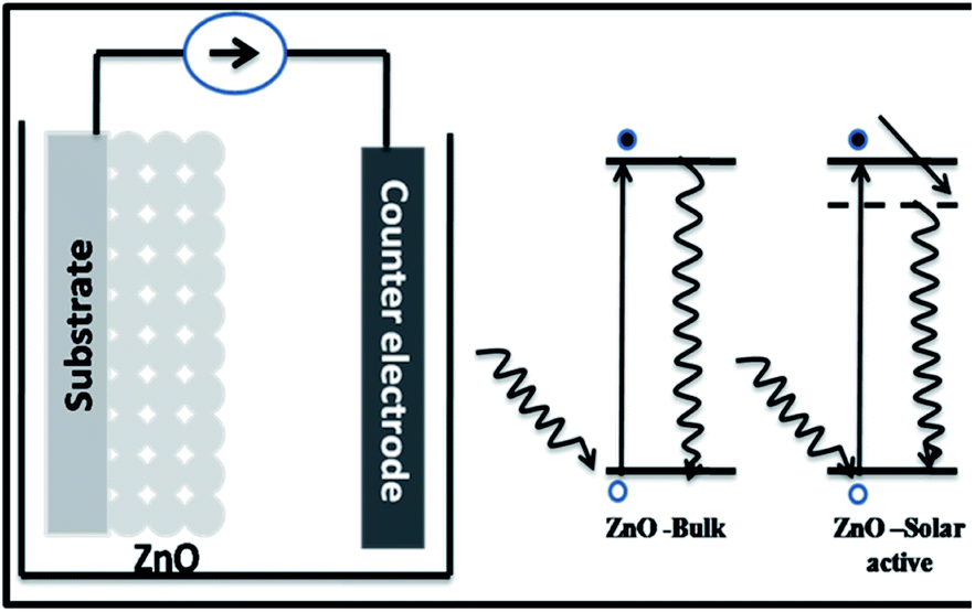
In order to understand the enhanced properties of SRZO photoanodes and to analyse their novelty with respect to photo-electrochemical application, it is important to carefully analyse the results presented above. The PEC behaviour of a photoanode is dependent on the physico-chemical properties of the material. All the films exhibited visible light optical absorption as shown in Fig. 3. This may be attributed to the favourable optical scattering occurring due to the depth of the film and the interaction of the photons at the film/substrate interface. The red-shift in the band gap of the SRZO photoanodes compared to bulk ZnO thus resulting in visible light absorption can be understood from the schematic presented in Fig. 7. It may be expected that the surface induced effects modulate the band-gap transitions in systems like zinc oxide. Further, the high donor densities calculated from the Mott–Schottky plots (on the order of 1017 cm−3) resulted in high PEC performance. The electrochemical impedance analysis of the SRZO films (see Fig. S6, ESI†) also showed lower charge transfer resistance of film B compared to C and D. However, although film A exhibits a lower charge transfer resistance than the others, its lower donor density (see Table S1, ESI†) by one order of magnitude compared to others and additionally its lower thickness make it comparatively less efficient. Thus, an efficient charge transfer and high donor density along with the maximum red shift in the band gap make film B an efficient nanostructured solar-responsive photoanode for visible light harvesting.
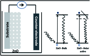 |
| | Fig. 7 Schematic showing the red-shift in the band gap of the SRZO photoanode compared to bulk ZnO. | |
5. Conclusion
To summarize, highly efficient solar active ZnO films were obtained by the versatile solution precursor plasma spray deposition technique. These photoanodes exhibited an enhanced photocurrent density of 390 μA under solar radiation. Further, the STH conversion efficiency from the evolved hydrogen was calculated to be 2.32%. These films exhibited visible light optical absorption. The surface induced effects modulating the band-gap transitions along with the favourable effects of optical scattering occurring due to the depth of nano-particulate film and the interaction of the incident photons at the film/substrate interface may be the reasons for this optical behaviour. The donor densities calculated from the MS plots were also found to be high. Thus, efficient visible light absorption and high donor density may be responsible for the superior quality performance of the films.
Conflicts of interest
There are no conflicts to declare.
Acknowledgements
The authors wish to thank Mr K. Ramesh Reddy, L. Venkatesh, and A. Satyanarayana for their help during deposition experiments and film characterization. Permission granted by Director, ARCI, Department of Science and Technology (DST) Lab, India, to publish the work is also gratefully acknowledged.
Notes and references
- A. Fujishima and K. Honda, Nature, 1972, 238, 37–38 CrossRef CAS PubMed.
- D. W. Hwang, H. G. Kim, J. S. Lee, J. Kim, W. Li and S. H. Oh, J. Phys. Chem. B, 2005, 109, 2093–2102 CrossRef CAS PubMed.
- S. W. Bae, P. H. Borse and J. S. Lee, Appl. Phys. Lett., 2008, 92, 104107 CrossRef.
- X. Xu, G. Liu, C. Randorn and J. T. S. Irvine, Int. J. Hydrogen Energy, 2011, 36, 13501–13507 CrossRef CAS.
- A. Wolcott, W. A. Smith, T. R. Kuykendall, Y. Zhao and J. Z. Zhang, Adv. Funct. Mater., 2009, 19, 1849–1856 CrossRef CAS.
- K. S. Ahn, Y. Yan, S. Shet, K. Jones, T. Deutsch, J. Turner and M. Al-Jassim, Appl. Phys. Lett., 2008, 93, 91–94 Search PubMed.
- S. Chen, W. Zhao, W. Liu and S. Zhang, Appl. Surf. Sci., 2008, 255, 2478–2484 CrossRef CAS.
- S. S. Shinde, P. S. Patil, R. S. Gaikwad, R. S. Mane, B. N. Pawar and K. Y. Rajpure, J. Alloys Compd., 2010, 503, 416–421 CrossRef CAS.
- S. M. Ji, P. H. Borse, H. G. Kim, D. W. Hwang, J. S. Jang, S. W. Bae, J. S. Lee, M. T. Team and S. E. Corporation, Phys. Chem. Chem. Phys., 2005, 7, 1315–1321 RSC.
- H. G. Kim, P. H. Borse, W. Choi and J. S. Lee, Angew. Chem., Int. Ed., 2005, 44, 4585–4589 CrossRef CAS PubMed.
- H. G. Kim, P. H. Borse, J. S. Jang, C. W. Ahn, E. D. Jeong and J. S. Lee, Adv. Mater., 2011, 23, 2088–2092 CrossRef CAS PubMed.
- A. Pareek, P. Paik and P. H. Borse, Dalton Trans., 2016, 45, 11120–11128 RSC.
- A. Pareek, H. G. Kim, P. Paik and P. H. Borse, J.Mater Chem A., 2017, 5, 1541–1547 RSC.
- J. H. Min, X. Y. Liang, B. Wang, Y. Zhao, Y. Guo and L. J. Wang, Adv. Mater. Res., 2011, 299–300, 436–439 CAS.
- S. U. M. Khan, M. Al-Shahry and W. B. Ingler, Science, 2002, 297, 2243–2245 CrossRef CAS PubMed.
- Y. Shaogui, Q. Xie, L. Xinyong, L. Yazi, C. Guohua, B. Science, C. W. Bay and H. Kong, Phys. Chem. Chem. Phys., 2004, 6, 659–664 RSC.
- Z. Zhang and P. Wang, J. Mater. Chem., 2012, 22, 2456–2464 RSC.
- Y. Wang, L. Cai, Y. Li, Y. Tang and C. Xie, Phys. E, 2010, 43, 503–509 CrossRef CAS.
- H. G. Kim, P. H. Borse, J. S. Jang, E. D. Jeong, O.-S. Jung, Y. J. Suh and J. S. Lee, Chem. Commun., 2009, 5889–5891 RSC.
- H. M. Chen, C. K. Chen, C. C. Lin, R. S. Liu, H. Yang, W. S. Chang, K. H. Chen, T. S. Chan, J. F. Lee and D. P. Tsai, J. Phys. Chem. C, 2011, 115, 21971–21980 CrossRef CAS.
- K. Sun, Y. Jing, C. Li, X. Zhang, R. Aguinaldo, A. Kargar, K. Madsen, K. Banu, Y. Zhou, Y. Bando, Z. Liu and D. Wang, Nanoscale, 2012, 4, 1515–1521 RSC.
- R. C. Fitzmorris, X. Yang, J. Z. Zhang, A. Wolcott, G. Wang, A. Sobo, Y. Li and F. Qian, Nano Lett., 2009, 9, 2331–2336 CrossRef PubMed.
- K.-S. Ahn, Y. Yan, S.-H. Lee, T. Deutsch, J. Turner, C. E. Tracy, C. L. Perkins and M. Al-Jassim, J. Electrochem. Soc., 2007, 154, B956 CrossRef CAS.
- E. M. Kaidashev, M. Lorenz, H. von Wenckstern, A. Rahm, H.-C. Semmelhack, K.-H. Han, G. Benndorf, C. Bundesmann, H. Hochmuth and M. Grundmann, Appl. Phys. Lett., 2003, 82, 3901–3903 CrossRef CAS.
- R. Dom, L. R. Baby, H. G. Kim and P. H. Borse, Int. J. Photoenergy, 2013, 2013, 1–9 CrossRef.
- R. Dom, H. G. Kim and P. H. Borse, CrystEngComm, 2014, 16, 2432–2439 RSC.
- V. Sharma, M. Prasad, P. Ilaiyaraja, C. Sudakar and S. Jadkar, Int. J. Hydrogen Energy, 2019, 44, 11459–11471 CrossRef CAS.
- V. Sharma, M. Prasad, A. Rokade, P. Ilaiyaraja, C. Sudakar and S. Jadkar, Energy Technol., 2019, 7, 233–239 CAS.
- M. A. Desai, A. N. Vyas, G. D. Saratale and S. D. Sartale, Int. J. Hydrogen Energy, 2019, 44, 2091–2127 CrossRef CAS.
- Y. J. Lu, C. F. Liu, C. C. Hu, J. H. Kuo and R. Boddula, Mater. Chem. Phys., 2017, 189, 56–63 CrossRef CAS.
- M. S. Islam, M. F. Hossain and S. M. A. Razzak, J. Photochem. Photobiol., A, 2016, 326, 100–106 CrossRef CAS.
- C. Liu, Y. Qiu, F. Wang, L. Li, Q. Liang and Z. Chen, Ceram. Int., 2017, 43, 5329–5333 CrossRef CAS.
- C. Yilmaz and U. Unal, Appl. Surf. Sci., 2016, 368, 456–463 CrossRef CAS.
- G. Z. Jia, Y. F. Wang and J. H. Yao, J. Phys. Chem. Solids, 2012, 73, 495–498 CrossRef CAS.
- R. Dom, G. Sivakumar, N. Y. Hebalkar, S. V. Joshi and P. H. Borse, Mater. Res. Bull., 2012, 47, 562–570 CrossRef CAS.
-
B. D. Cullity and S. R. Stock, Elements of X-ray diffraction, 2014 Search PubMed.
- J. Tauc, R. Grigorovici and A. Vancu, Phys. Status Solidi, 1966, 15, 627–637 CrossRef CAS.
- N. Kislov, S. S. Srinivasan, Y. Emirov and E. K. Stefanakos, Mater. Sci. Eng., B, 2008, 153, 70–77 CrossRef CAS.
- C. Yao, B. Wei, H. Ma, H. Li, L. Meng, X. Zhang and Q. Gong, J. Power Sources, 2013, 237, 295–299 CrossRef CAS.
- M. C. Huang, T. Wang, B. J. Wu, J. C. Lin and C. C. Wu, Appl. Surf. Sci., 2016, 360, 442–450 CrossRef CAS.
- W. Zhao, Z. Wang, X. Shen, J. Li, C. Xu and Z. Gan, Int. J. Hydrogen Energy, 2012, 37, 908–915 CrossRef CAS.
- R. C. Pawar, J. S. Shaikh, A. A. Babar, P. M. Dhere and P. S. Patil, Sol. Energy, 2011, 85, 1119–1127 CrossRef CAS.
Footnotes |
| † Electronic supplementary information (ESI) available. See DOI: 10.1039/d0na00139b |
| ‡ Present address: M.V.S.R. Engineering College, Nadergul, Hyderabad-501510, India. |
|
| This journal is © The Royal Society of Chemistry 2020 |
Click here to see how this site uses Cookies. View our privacy policy here. 
 Open Access Article
 This Open Access Article is licensed under a Creative Commons Attribution-Non Commercial 3.0 Unported Licence
 a,
Sivakumar
Govindarajan
a,
Sivakumar
Govindarajan