
 Open Access Article
 This Open Access Article is licensed under a Creative Commons Attribution-Non Commercial 3.0 Unported Licence
Aluminium metal–insulator–metal structure fabricated by the bottom-up approach†
Rie
Watanabe
a,
Mai
Mita
a,
Takayuki
Okamoto
 b,
Toshihiro
Isobe
a,
Akira
Nakajima
a and
Sachiko
Matsushita
*a
b,
Toshihiro
Isobe
a,
Akira
Nakajima
a and
Sachiko
Matsushita
*a
aDepartment of Materials Science and Engineering, School of Materials and Chemical Technology, Tokyo Institute of Technology S7-7, 2-12-1 Ookayama, Meguro-ku, Tokyo 152-8550, Japan. E-mail: matsushita.s.ab@m.titech.ac.jp
bRiken, 2-1 Hirosawa, Wako, Saitama 351-0198, Japan
First published on 20th April 2020
Abstract
Plasmonic color is an elegant color resulting from light absorption and emission induced by collective oscillation of free electrons in a metal and enables unprecedented new color expression. In particular, Al plasmonic color is highly desirable because of the low cost and high stability of Al. Here, we report a new cost-effective, wide-area fabrication method for an Al metal–insulator–metal (MIM) plasmonic nanostructure using a vapor deposition and sintering process.
Introduction
Color plays an important role in our lives; it is used in many applications to improve convenience and safety and to enhance beauty and design. At present, the main colorants are dyes that absorb light via electronic transitions of the dye molecules. The disadvantage of using dyes is their tendency to fade.1 In addition, using different pigments or dyes for each color can complicate recycling.2,3 In recent years, research2,4 and practical applications of structural colors have progressed; expectations are now especially high for plasmonic color.5 Plasmonic color results from light absorption and emission induced by collective oscillations of free electrons in a metal. Color generated under this principle is less prone to degradation.In the field of plasmonics, precious metals such as Au and Ag have been extensively investigated.6–8 These metals have low ohmic losses and strong optical dipole interactions.9 However, the Au plasmon resonance wavelength does not cover the entire visible range and the lifetime of plasmon resonance is short; in addition, Ag exhibits low stability under atmospheric exposure. The further development and practical application of plasmonics10–14 necessitates the development of alternative materials.15,16 In the present study, we focus on an abundant and inexpensive metal, Al, that exhibits plasmon resonance in the entire visible-light region17 and is stabilized by a natural oxide protective film.18
Recently, Al plasmonic colors based on metal–insulator–metal (MIM) structures19–26 composed of a bottom metal layer, middle insulator layer, and top metal nanostructure have been reported. However, as far as we know, no mass production method for Al MIM structures has been reported. The dewetting process is a mass production method that can be used to form a metal island on an insulator. However, for the dewetting process to be used, there must be no chemical bond at the interface between the metal and the insulator and there must be a difference in the thermal expansion coefficients between the metal and the insulator material. Therefore, Al nanoislands do not form in the normal dewetting process because Al easily bonds with O2 in the air. In the present study, we report the bottom-up preparation of an Al MIM structure via vapor deposition and heat treatment. This method enables the easy and inexpensive fabrication of large-area Al MIM structures.
Experimental
Fabrication of MIM structures
The fabrication scheme of the Al MIM nanostructures is shown in Fig. 1. Borosilicate glass (Corning 1737) was cut using a plate cutter (TLC plate cutter, OM Laboratory) to produce a 15 × 15 × 1.0 mm3 glass substrate. The substrate was immersed in 99.5% ethanol (Wako) and sonicated for 15 min to remove the coating agent on the glass surface. Next, Al (Nippaku foil, Mitsubishi Aluminium) was deposited onto the substrate using a vapor deposition device (SVC-700TMSG/7PS80, Sanyu Electron). The obtained film thickness was 178.0 ± 19.5 nm, as measured by profilometry (N = 25, Dektak 6M, Veeco). The atmospheric pressure was 4 × 10⁻³ Pa, the distance between the substrate and the vapor deposition source was 9.5 cm, and an Al2O3-coated W basket (basket type boat B-3, Nilaco) was used as the vapor-deposition boat. Thereafter, an Al2O3 layer as the insulator layer was formed on the first metal layer by heating using an electric furnace (KDF-S70, Denken). The furnace temperature was increased to 450 °C at a rate of 2.5°C min−1, maintained at this temperature for 30 min, and then allowed to cool naturally to room temperature. Subsequently, 50, 60, or 70 nm-thick Al was deposited onto the sample in the same manner and the sample was subsequently heated. The furnace temperature was increased to 450, 500, 550, or 600 °C at a rate of 5 °C min−1, maintained at the target temperature for 30 min, and then allowed to cool naturally to room temperature. A nanosized non-oxidized region remained in the second Al2O3 layer, and a MIM nanostructure was thus obtained.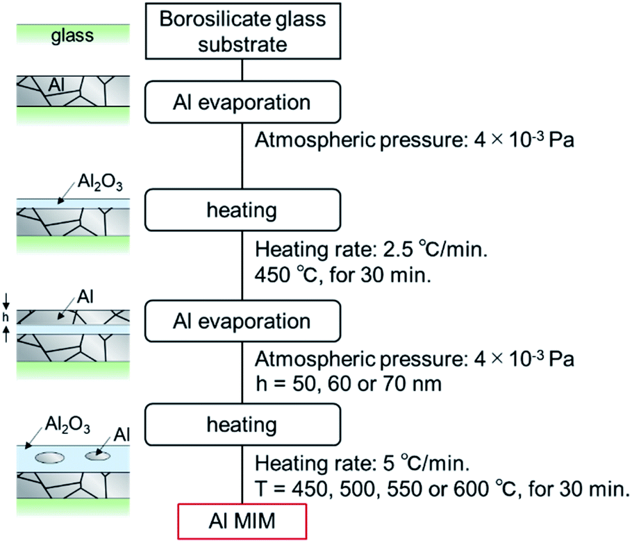 | ||
| Fig. 1 Fabrication procedure of the Al MIM structure and a schematic of a sample in each stage of the process. | ||
If the size of the unoxidized Al particles is different, samples of different colors should be obtained.27,28 Thus, the second-layer Al film thickness and the second-layer heating temperature were adjusted as previously described. Each sample was named as Al(second Al layer thickness/nm) − (second layer heating temperature/°C).
Optical measurements
To evaluate the color of the samples, reflection spectra were recorded with a UV-vis spectrophotometer (V-770, Jasco) equipped with an integrating sphere unit (ISN-923, Jasco). The measurement range was 200 to 1000 nm, and a BaSO4 white plate was used for the baseline measurement. The incident angle was 5° in the measurement of the spectrum including the specular reflection component and the diffuse reflection component (SCI, Specular Component Include) and 0° in the measurement of the spectrum including only the diffuse reflection component (i.e., excluding the specular reflection component) (SCE, specular component excluded). Here, the normal incidence to the sample was set as 0°.Confirmation of structures
Secondary electron image observations were performed by field-emission scanning electron microscopy (FE-SEM, JSM-7500F, JEOL). The acceleration voltage was 10.0 kV, the emission current was 10 μA, and the working distance was 8.0 mm. Os was sputtered to a thickness of approximately 5 nm as a conductive treatment. Elemental analysis was conducted in the depth direction by Auger electron spectroscopy (AES, JAMP-9500F, JEOL). To determine the size of the nanostructures, energy-dispersive X-ray spectroscopy (EDX) mapping was performed by FE-SEM (SU9000, Hitachi High-Tech); the acceleration voltage was 30 kV.Numerical simulations
The structure of the sample was modeled from the obtained EDX mapping diagram of the sample cross section. The scattering, extinction, and absorption cross sections were calculated by the finite-difference time-domain (FDTD) method. The electric field distribution was also calculated. The cell size for the FDTD calculation was 2.0 nm. The computation space was terminated with convolutional perfectly matched layers. The relative permittivity of metal was fitted by a Drude–Lorentz model. A Gaussian temporal–pulse plane wave normal to the substrate from the top was used to calculate the cross-section spectra. In the calculation of scattering and extinction cross sections, the specular reflection component was removed.Results and discussion
Let us summarize our fabrication concept. Even when the sputtering process is used, the fabricated Al film is not a single crystal; it is composed of Al nanograins. In this case, the oxidation process progresses from the grain boundaries. We attempted to stop the oxidation process halfway and obtain Al nanoparticles encapsulated by Al2O3. Research on the formation of a surface oxide film on an Al film by heating has a long history. Numerous studies have been conducted from a practical point of view. The oxide film growth rate varies depending on the heating temperature and heating time, which enables the oxide film thickness to be controlled.29–31Sample photographs in each step before the second heating are shown in Fig. S1†. Although the specular reflection component became visually stronger after the first heating, no specific color was observed even after the second vapor deposition. SEM images (Fig. S1†) show that no change in roughness on the order of several tens of nanometers occurred. Reflection spectra after each process are shown in Fig. 2. Because the reflectance of all SCE spectra were weak, the surface of the sample was optically smooth and the smoothness did not substantially change even after the first heating and second deposition. Because no specific color was observed before the second heating, no nanostructure that generates plasmonic color was present. Fig. 3 shows optical images after the second heating. The incident light source for these images was a fluorescent lamp. Some of the samples heated at 450 °C or 500 °C for the second time were yellowish, and all of them exhibited a strong specular reflection component. By contrast, the samples heated at 550 °C or 600 °C were colorful, appearing blue, orange, yellow, green, or purple.
 | ||
| Fig. 2 SCI and SCE spectra of Al-60-600 in each process before the second heating. | ||
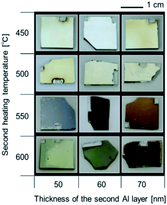 | ||
| Fig. 3 Optical images of the samples with different Al film thicknesses (second) and subjected to a second heating temperature. | ||
The UV-vis reflection spectra are shown in Fig. 4. Because the intensity of the SCE spectra increased more than before the second heating, scatters were clearly formed on or inside the samples.
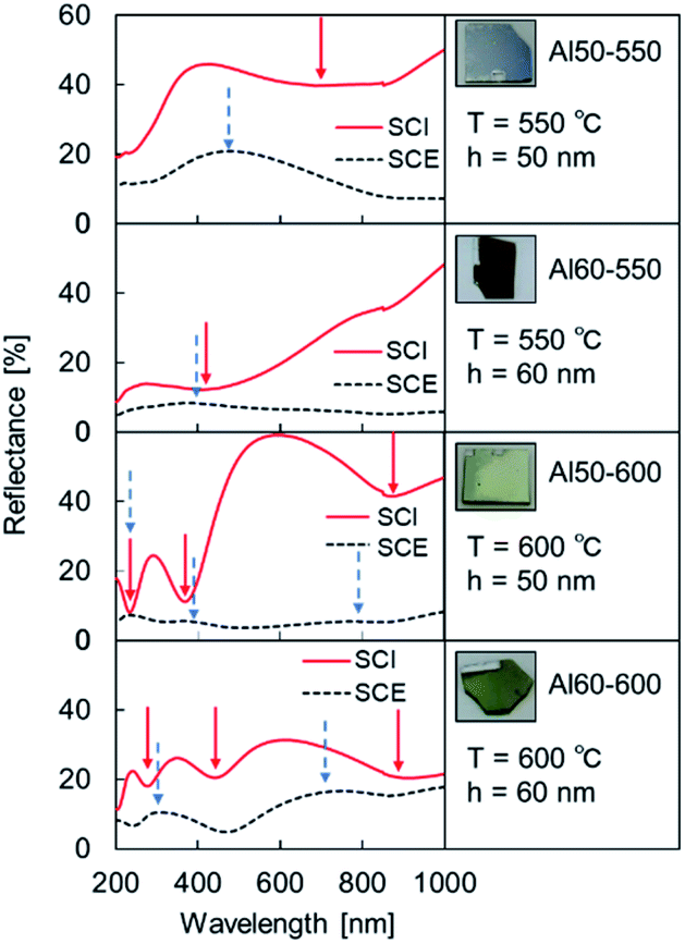 | ||
| Fig. 4 SCI spectra and SCE spectra of Al MIM samples after the second heating. The Al film thickness of the second layer was 50 or 60 nm, and the second heating temperature was 550 or 600 °C. | ||
The trough position in the wavelength range below 400 nm in the SCI spectrum coincides with the peak position in the SCE spectrum for all of the samples. However, at wavelengths longer than 400 nm, a difference between the trough position in the SCI spectrum and the peak position in the SCE spectrum was confirmed for each sample. These results suggest that some optical modes6,32–35 exist in addition to the thin-film interference and localized surface plasmon mode.
An SEM image of sample Al-60-600 is shown in Fig. 5(a). The formation of bulges and depressions with an area of several hundred square nanometers to several square micrometers was confirmed, and the roughness of the surface increased. From the above, it is considered that the top and inside of the sample were non-uniform.
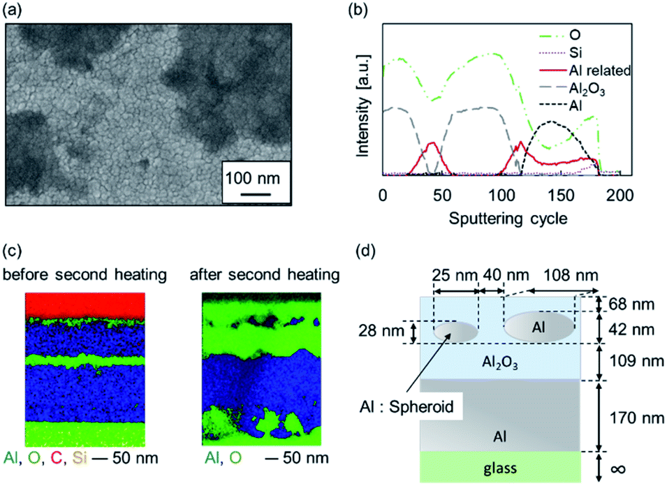 | ||
| Fig. 5 Structural observation and elemental analysis of Al-60-600. (a) SEM image of sample surface. (b) Auger electron spectroscopic analysis results in the depth direction; the orange line is the intensity of the signal of the part considered to be less oxidized between the deposited Al layers. (c) Cross-sectional EDX mapping images of the sample before and after the second heating. (d) Calculation model. | ||
To explore the structure of the samples, we conducted AES analysis in the depth direction to determine which elements were present (Fig. S2†). In AES, the depth that can be probed in a single cycle is approximately several nanometers (depending on the material). The results from 1370 eV to 1400 eV indicate that both Al and Al2O3 were present at approximately 50 cycles and 120 cycles. The 50 cycles correspond to the lower part of the second Al thin film. Therefore, the second layer of Al was not completely oxidized and a metallic component remained, as we expected. However, the profiles corresponding to this region could not be properly fitted using the standard spectra of Al and Al2O3 reported in Auger databases (shown as a solid line labeled “Al related” Fig. 5(b)).
The structure of this Al-related second layer was subsequently investigated. Fig. 5(c) shows the cross-sectional EDX mapping images obtained by FE-SEM. These images confirm that the Al layer and the oxide layer were flat until the second heating. However, after the second heating, some nanoregions were less oxidized. These nanostructures might be able to induce plasmonic color. The structure was modeled as shown in Fig. 5(d) for later simulation, and the dimensions are also shown. These nanoregions are represented by oblate spheroids (ESI 3†).
Four types of models, as shown in Fig. 6(a–d), were created from the EDX mapping results, and simulations were performed. The simulation spectra relatively fit with Fig. 4 (Al-60-600). In all of the models with a metal film and nanoparticles (Fig. 6(a) and (b)), scattering peaks appeared near 250 and 380 nm; by contrast, no peak was observed for structures without a metal film (Fig. 6(c)). Here, the Fabry–Pérot modes are observed at approximately 250 and 350 nm without a nanoparticle (Fig. 6(d)). From these discussions, we deduced that these peaks may be caused by the scattering of Fabry–Pérot mode by the particle.36
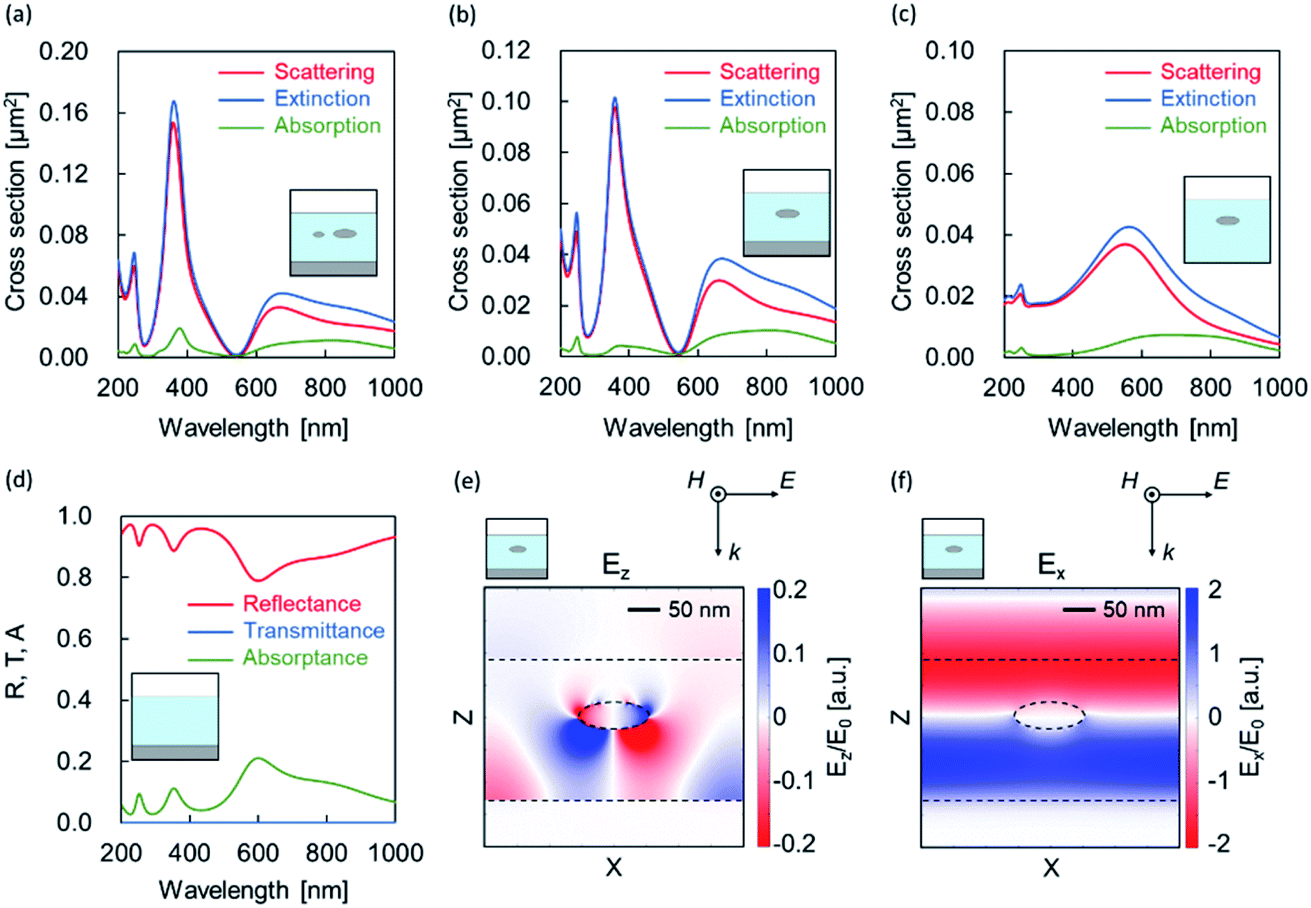 | ||
| Fig. 6 Calculation results of scattering, extinction, and absorption cross sections for each model. (a–d) Results of electric field distribution calculations at a resonant wavelength 550 nm in the (e) Z and (f) X directions for a model consisting of an Al thin film and a larger Al nanostructure. The dotted line represents the interface. | ||
In the calculation results of the structure composed of an oxide layer and a metal nanoparticle without a metal film (Fig. 6(c)), a scattering peak was confirmed near 550 nm. This peak is attributed to the localized surface plasmon resonance caused by metal nanoparticles. We also observed a Fabry–Pérot mode at ∼600 nm without a nanoparticle in Fig. 6(d). From these spectral shapes, we considered that the dips near 550 nm and peaks at approximately 650 nm in Fig. 6(a) and (b) a originated from the Fano resonance37 due to the interference between the localized surface plasmon mode and the Fabry–Pérot mode.
To confirm the aforementioned hypothesis, we calculated the electric field distribution at 550 nm for the model in Fig. 6(b). Fig. 6(e) shows the z component of the electric field, in which weak polarization such as a quadrupole appeared in the nanoparticle. However, the x component shown in Fig. 6(f) was hardly disturbed by the nanoparticles. From these distributions, we confirmed the dip was caused by the Fano resonance.
Conclusions
Here, we report a new Al MIM structure fabrication method from the viewpoint of mass production. This method is a combination of vapor deposition and heating. Under certain conditions, the plasmonic colors were generated by metallic nanoparticles inside an Al2O3 film. The calculation results from the simulation models suggest that, in this system, in addition to the Fabry–Pérot mode, Fano resonance due to interference between the localized surface plasmon mode occurred. That is, the color can be controlled by the thickness of the insulator layer and the size of the metal nanoparticles. Plasmonic color was successfully produced by the production method proposed in this work.Author contributions
RW fabricated the samples. RW recorded the spectra and took optical and SEM images of the samples. TO conducted the computer simulations. RW, MM, TO, and SM considered the optical properties of the samples. TI, AN, and SM supervised RW. RW and SM wrote the paper.Conflicts of interest
There are no conflicts to declare.Acknowledgements
Tokyo Institute of Technology Ookayama Materials Analysis Division, Technical Department is acknowledged for conducting the AES measurements and EDX mapping and renting the SEM. The calculations were performed using the RIKEN HOKUSAI GreatWave Facility.Notes and references
- R. Mudachathi and T. Tanaka, Sci. Rep., 2017, 7, 1199 CrossRef PubMed.
- M. Keshavarz Hedayati and M. Elbahri, Plasmonics, 2016 DOI:10.1007/s11468-016-0407-y.
- J. S. Clausen, E. Højlund-Nielsen, A. B. Christiansen, S. Yazdi, M. Grajower, H. Taha, U. Levy, A. Kristensen and N. A. Mortensen, Nano Lett., 2014, 14, 4499–4504 CrossRef CAS PubMed.
- S. Kinoshita, S. Yoshioka and K. Kawagoe, Proc. R. Soc. London, Ser. B, 2002, 269, 1417–1421 Search PubMed.
- M. Miyata, H. Hatada and J. Takahara, Nano Lett., 2016, 16, 3166–3172 CrossRef CAS PubMed.
- F. Ding, Y. Yang, R. A. Deshpande and S. I. Bozhevolnyi, Nanophotonics, 2018, 7, 1129–1156 CAS.
- M. G. Nielsen, A. Pors, O. Albrektsen and S. I. Bozhevolnyi, Opt. Express, 2012, 20, 13311–13319 CrossRef PubMed.
- G. Schaffernak, M. K. Krug, M. Belitsch, M. Gašparić, H. Ditlbacher, U. Hohenester, J. R. Krenn and A. Hohenau, ACS Photonics, 2018, 5, 4823–4827 CrossRef CAS PubMed.
- R. H. Siddique, J. Mertens, H. Hölscher and S. Vignolini, Light: Sci. Appl., 2017, 6, e17015 CrossRef CAS PubMed.
- K. V. Sreekanth, Y. Alapan, M. ElKabbash, E. Ilker, M. Hinczewski, U. A. Gurkan, A. De Luca and G. Strangi, Nat. Mater., 2016, 15, 621–627 CrossRef CAS PubMed.
- A. V. Kabashin, P. Evans, S. Pastkovsky, W. Hendren, G. A. Wurtz, R. Atkinson, R. Pollard, V. A. Podolskiy and A. V. Zayats, Nat. Mater., 2009, 8, 867–871 CrossRef CAS PubMed.
- V. Caligiuri and A. De Luca, J. Phys. D: Appl. Phys., 2016, 49, 08LT01 CrossRef.
- H.-S. Ee, H.-G. Park and S.-K. Kim, Appl. Opt., 2016, 55, 1029–1033 CrossRef CAS PubMed.
- L. P. Hackett, A. Ameen, W. Li, F. K. Dar, L. L. Goddard and G. L. Liu, ACS Sensors, 2018, 3, 290–298 CrossRef CAS PubMed.
- A. Sobhani, A. Manjavacas, Y. Cao, M. J. McClain, F. J. Garcia de Abajo, P. Nordlander and N. J. Halas, Nano Lett., 2015, 15, 6946–6951 CrossRef CAS PubMed.
- F. Zhang, J. Proust, D. Gérard, J. Plain and J. Martin, J. Phys. Chem. C, 2017, 121, 7429–7434 CrossRef CAS.
- M. W. Knight, N. S. King, L. Liu, H. O. Everitt, P. Nordlander and N. J. Halas, ACS Nano, 2014, 8, 834–840 CrossRef CAS PubMed.
- D. S. Sundaram, V. Yang and V. E. Zarko, Combust., Explos. Shock Waves, 2015, 51, 173–196 CrossRef.
- S. Murthy, H. Pranov, N. A. Feidenhans'l, J. S. Madsen, P. E. Hansen, H. C. Pedersen and R. Taboryski, Nanoscale, 2017, 9, 14280–14287 RSC.
- H. Alaeian and J. A. Dionne, Phys. Rev. B: Condens. Matter Mater. Phys., 2014, 89, 075136 CrossRef.
- J. A. Dionne, L. A. Sweatlock, H. A. Atwater and A. Polman, Phys. Rev. B: Condens. Matter Mater. Phys., 2006, 73, 035407 CrossRef.
- I. Avrutsky, I. Salakhutdinov, J. Elser and V. Podolskiy, Phys. Rev. B: Condens. Matter Mater. Phys., 2007, 75, 241402 CrossRef.
- J. Kim, E. G. Carnemolla, C. DeVault, A. M. Shaltout, D. Faccio, V. M. Shalaev, A. V. Kildishev, M. Ferrera and A. Boltasseva, Nano Lett., 2018, 18, 740–746 CrossRef CAS PubMed.
- V. Caligiuri, M. Palei, G. Biffi, S. Artyukhin and R. Krahne, Nano Lett., 2019, 19, 3151–3160 CrossRef CAS PubMed.
- R. Verre, Z. J. Yang, T. Shegai and M. Käll, Nano Lett., 2015, 15, 1952–1958 CrossRef CAS PubMed.
- K. Moon, T.-W. Lee, Y. Lee and S.-H. Kwon, Applied Sciences, 2017, 7, 86 CrossRef.
- J. R. Krenn, G. Schider, W. Rechberger, B. Lamprecht, A. Leitner, F. R. Aussenegg and J. C. Weeber, Appl. Phys. Lett., 2000, 77, 3379–3381 CrossRef CAS.
- K. Imura, T. Nagahara and H. Okamoto, J. Phys. Chem. B, 2005, 109, 13214–13220 CrossRef CAS PubMed.
- N. Cabrera and N. F. Mott, Rep. Prog. Phys., 1949, 12, 163 CrossRef CAS.
- K. R. Lawless, Rep. Prog. Phys., 1974, 37, 231 CrossRef CAS.
- F. H. Stott, Rep. Prog. Phys., 1987, 50, 861 CrossRef CAS.
- N. Liu and H. Giessen, Angew. Chem., Int. Ed., 2010, 49, 9838–9852 CrossRef CAS PubMed.
- N. Liu, M. Mesch, T. Weiss, M. Hentschel and H. Giessen, Nano Lett., 2010, 10, 2342–2348 CrossRef CAS PubMed.
- W. Cai, U. K. Chettiar, H.-K. Yuan, V. C. de Silva, A. V. Kildishev, V. P. Drachev and V. M. Shalaev, Opt. Express, 2007, 15, 3333–3341 CrossRef.
- C. Wu, B. Neuner, G. Shvets, J. John, A. Milder, B. Zollars and S. Savoy, Phys. Rev. B: Condens. Matter Mater. Phys., 2011, 84, 075102 CrossRef.
- J. A. Dionne, L. A. Sweatlock, H. Atwater and A. Polman, Phys. Rev. B: Condens. Matter Mater. Phys., 2005, 72, 075405 CrossRef.
- M. F. Limonov, M. V. Rybin, A. N. Poddubny and Y. S. Kivshar, Nat. Photonics, 2017, 11, 543–554 CrossRef CAS.
Footnote |
| † Electronic supplementary information (ESI) available: Visual appearance and SEM images of sample before second heating, the result of auger electron spectroscopy analysis of Al-60-600. See DOI: 10.1039/d0na00082e |
| This journal is © The Royal Society of Chemistry 2020 |