
 Open Access Article
 This Open Access Article is licensed under a Creative Commons Attribution-Non Commercial 3.0 Unported Licence
Flexible transparent graphene laminates via direct lamination of graphene onto polyethylene naphthalate substrates†
Ismael G.
Serrano
 a,
J.
Panda
a,
Tomas
Edvinsson
b and
M. Venkata
Kamalakar
*a
a,
J.
Panda
a,
Tomas
Edvinsson
b and
M. Venkata
Kamalakar
*a
aDepartment of Physics and Astronomy, Uppsala University, Box 516, SE-751 20 Uppsala, Sweden. E-mail: venkata.mutta@physics.uu.se
bDepartment of Materials Science and Engineering, Uppsala University, Box 534, SE-751 21 Uppsala, Sweden
First published on 9th June 2020
Abstract
Graphene, with its excellent electrical, mechanical, and optical properties, has emerged as an exceptional material for flexible and transparent nanoelectronics. Such versatility makes it compelling to find new pathways to lay graphene sheets onto smooth, flexible substrates to create large-scale flexible transparent graphene conductors. Here, we report the realization of flexible transparent graphene laminates by direct adhesion of chemical vapor deposition (CVD) graphene on a polyethylene naphthalate (PEN) substrate, which is an emerging standard for flexible electronics. By systematically optimizing the conditions of a hot-press technique, we have identified that applying optimum temperature and pressure can make graphene directly adhere to flexible PEN substrates without any intermediate layer. The resultant flexible graphene films are transparent, have a standard sheet resistance of 1 kΩ with high bending resilience, and high optical transmittance of 85%. Our direct hot-press method is achieved below the glass transition temperature of the PEN substrate. Furthermore, we demonstrate press-assisted embossing for patterned transfer of graphene, and hence it can serve as a reliable new means for creating universal, transparent conducting patterned films for designing flexible nanoelectronic and optoelectronic components.
1 Introduction
Experimentally isolated in 2004, within a decade, graphene's extraordinary electrical, mechanical, and optical properties1 showed great potential for applications ranging from electronics, photonics, optoelectronics, solar cells, light-emitting diodes, touch screen technologies, photodetectors, membranes, and spintronics.2–7 Graphene is ideal for new developments in flexible electronics due to its exceptional resilience8 and conductivity in atomically thin layers. Also, there exists tremendous scope for flexible batteries, transparent electrodes, and embedded electronic sensors. For such next-generation flexible electronic applications, transparent, conducting, and flexible graphene sheets are a prime necessity. Central to graphene-based flexible surfaces and transparent electrodes applications is the challenge to devise a scalable and affordable method to obtain large-scale flexible graphene systems.9,10 Chemical vapor deposited (CVD) graphene is the scalable form of graphene that can be transferred to any substrate of choice, which makes it the most technologically relevant form of graphene. CVD graphene is generally grown on Cu or Ni substrates and then transferred.11–13 The process involves coating the graphene on copper/nickel substrate with a layer of polymethylmethacrylate (PMMA) to ensure mechanical stability when the metal is chemically etched away, leaving behind graphene covered with PMMA film. The graphene|PMMA is then placed on a substrate, dried, and subsequently PMMA is dissolved to accomplish the total transfer of graphene. However, often left-over PMMA residues have been observed to reduce the quality, electrical properties and uniformity of graphene.14–16 This has been tackled by optimizations using chemical methods to remove such residues and improve graphene performance.17 However, avoiding PMMA by directly transferring graphene using transfer techniques could lead to several new advantages for reducing the cost and processing time immensely, in particular for industrial applications. This prospect has generated interest in new ways of direct transfer techniques without PMMA resist.18 However, such processes lead to new challenges for polymer substrates,19 because such polymers cannot tolerate the annealing temperature or some solvents. Polyethylene terephthalate (PET) and polyethylene (PE) are the currently used polymer substrates for transparent-flexible graphene applications. Earlier, graphene contact transfer onto PET has been achieved using an adhesion layer of ethylene-vinyl acetate (EVA),10,18,20 or thermal release tape.6 Also, large scale roll manufacturing ethylene-vinyl acetate (EVA) assisted transfer,21 roll to roll production using EVA, or adhesion tape3,9 have been demonstrated. A direct transfer without such an intermediate layer, however, has so far proved challenging.22 In particular, for standard polymer substrates such as PET, it is difficult to perform direct dry-transfer of CVD graphene15 due to low processable temperature. Recent developments have revealed another important low roughness polymer substrate called polyethylene naphthalate (PEN), which due to its low roughness and high limit of processable temperature, shows new promise for flexible nanoelectronics developments and development of direct dry-transfer techniques.In this work, we employ polyethylene naphthalate (TEONEX PEN substrates from Dupont Teijin films), a new age polyethylene semi-crystalline flexible substrate,23 highly promising for flexible electronics, to demonstrate direct graphene lamination on to PEN with no intermediate layer, leading to fast, affordable and large-scale graphene flexible samples. PEN is a transparent substrate that has many improved abilities, for instance, higher glass transition temperature (Tg = 123 °C) compared to PET (Tg = 80 °C), greater process capable temperature (∼150 °C) and overall root mean square roughness (∼1.5 nm).23 Recent experiments have shown high performance in graphene devices on PEN substrates.5 These specific attributes open up doors for exploring the direct lamination of graphene through controlled temperature and pressure.
2 Experimental section
2.1 Sample preparation
To prepare direct-laminated flexible graphene samples, we use a nanoimprint press to transfer CVD graphene (Graphena Inc.) onto a PEN substrate with no-intermediate layers. Nanoimprint technique is generally used for printing-stamping metallic masks on special resists for lithographic processes, with the assistance of heat and pressure to stamp the pattern. This method is known to be faster and provides better resolution than conventional photolithography, and it is widely used on large-scale chips fabrication.24 The possibility of quick pattering makes it a versatile technique not just for exploring direct lamination but also for selective transfer of designs. We, therefore, employ this technique to transfer graphene on flexible PEN and perform characterization to understand the quality of such films electrically and optically. Furthermore, we show that our method can also enable the transfer of a pre-patterned CVD graphene on Cu, which has been previously patterned with a stencil mask and reactive ion plasma etching (RIE).2.2 Characterization
The sheet resistance and large-scale continuity of the transferred graphene were characterized by a 4-probe station AIT 4-probe station model CMT-SR2000N. The composition of the samples was studied by Raman spectroscopy equipment Renishaw model InVia, using an excitation laser wavelength of 532 nm. The transmittance was measured by Ocean Optics high-resolution HR2000+ photo-spectrometer using direct aligned optical fibers in perpendicular mode and a collimating lens before the detector, and a PerkinElmer Ltd. model Lambda 900.3 Results and discussion
An outline of the lamination process developed here is illustrated in Fig. 1. It consists of three main steps: (a) pressure and heat-assisted lamination, (b) chemical etching of Cu substrate, followed by (c) final cleaning with deionized water. For the lamination of graphene onto the PEN surfaces, it is essential to find optimized pressure and heat to increase the adhesion of graphene to the PEN substrate by enhancing the surface activation of PEN. A well-adhered graphene layer can withstand copper etching and subsequent water cleaning. In our experiments, we use commercial CVD graphene grown on 18 μm thick Cu layer, a 125 μm thick PEN substrate, and a nanoimprint system capable of applying a controlled pressure of 20–45 bar, and temperatures up to 125 °C. As shown in Fig. 1, first, we put the PEN layer in the nanoimprint, and a Gr/Cu layer is then placed with the graphene facing down. A layer of aluminum foil is then placed covering the whole area of the sample holder. To optimize the quality of lamination of graphene on PEN with pressure and heat conditions, we have performed lamination under different conditions at various temperatures in the range 90–125 °C and pressures in the range of 20–45 bar. In the nanoimprint setup, when a specific set temperature is reached, a cavity filled with compressed air is created between the protective layer and the top part (shown in Fig. 1a), producing the controlled pressure. After the lamination process, the copper layer with graphene sticks to the PEN substrate. As shown in Fig. 1b, the copper layer is then etched out in a 0.5 M solution of FeCl3 for 4 hours, and subsequently, the sample is rinsed in deionized water (Fig. 1c).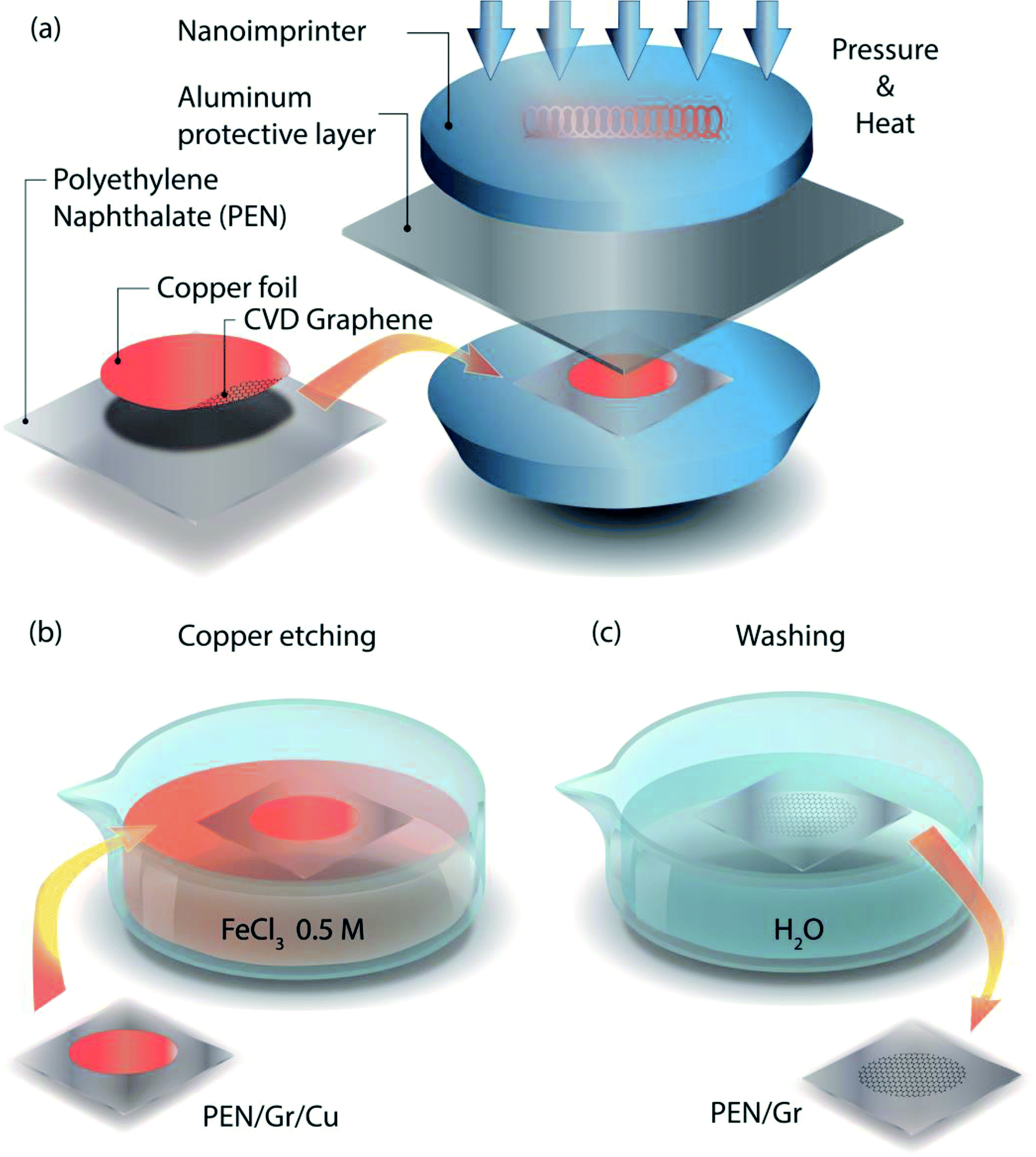 | ||
| Fig. 1 (a) Schematic representation of the nanoimprint system and lamination process, (b) Cu etching process, and (c) DI water rinsing. | ||
A graphene|Cu sample sticking to the PEN substrate after the lamination is shown in Fig. 2a. The sample is placed in an FeCl3 etchant solution, whereby the Cu layer is etched away. The final graphene on PEN is shown in Fig. 2b, with the bright contrast of the laminated graphene area from the PEN, indicating a successful lamination. To explore the quality of the transfer, we have examined several laminated graphene|PEN samples under an optical microscope. In Fig. 2c–f, we show samples laminated under different pressure and temperature conditions (samples laminated at lower temperatures are shown in supplementary information Fig. S1†). The vertical dark line corresponds to the border of the initial graphene on Cu sample, and it helps in determining the boundary of the PEN transferred area from the rest of the sample. Fig. 2e shows a sample treated at 115 °C under 45 bar, where a clear difference in contrast is noticed between the two areas. Fig. 2f shows a sample treated at 125 °C at 45 bar, for which the contrast changes abruptly between the two areas. These results suggest that pressure and temperature are crucial factors determining the quality of the resulting sample. In the following, we will discuss the details of large-scale characterization that we used to assess the quality of these samples.
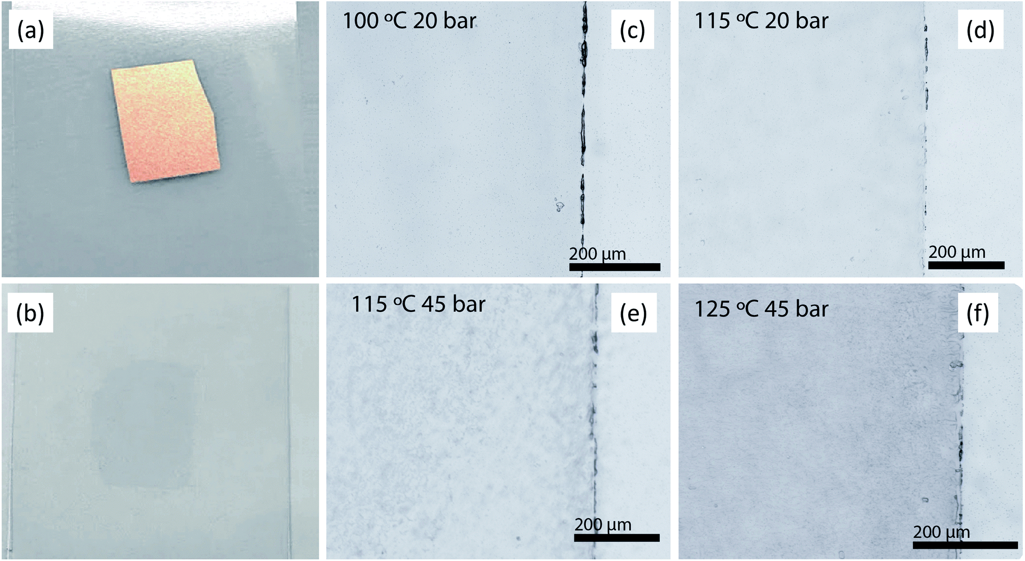 | ||
| Fig. 2 (a) PEN/Gr/Cu after lamination, (b) PEN/Gr after copper etching and rinsing. Optical microscope images of (c) sample 4 (100 °C, 20 bar), (d) sample 7 (115 °C, 20 bar), (e) sample 9 (115 °C, 45 bar), (f) sample 15 (125 °C, 45 bar). | ||
It is worth noting that the lamination achieved in this work, has not been previously performed with polyethylene naphthalate-based substrates. One of the critical parameters is the surface wettability and is one of the most studied interfacial phenomena in polymeric substrates used in deposition approaches, e.g., for inkjet printing and slot coating. Surfaces that have a contact angle higher than 90° and lower than 150° are defined as hydrophobic surfaces and become superhydrophobic surfaces for angles higher than 150°. PEN has a contact angle of 76.55°, a value similar to PET contact angle (78.57°).25 According to previous works,18 wettability is critical during the copper etching process, and it is considered a limiting factor for direct lamination on PET. The possibility of direct graphene lamination transfer has been controversial, with reports for PET substrate,22 contradicting studies that suggest the need for intermediate wettability layers.18,26 This is because a direct transfer of graphene is not possible due to the low glass transition temperature of PET, which limits any possibility to enhance the surface wettability by increasing the temperature. Transfer on PET at 130 °C is still a challenge because of its lower glass transition temperature ∼80 °C.27 On the other hand, employing PEN with its higher glass transition temperature, it is possible to overcome the problem of wettability, which enables us to demonstrate the direct transfer of graphene on a PEN flexible substrate.
To analyze the laminated samples prepared under different conditions of temperatures and pressures, we performed large-scale electrical characterization of the transferred graphene sheets. For this, the sheet resistance measurement of graphene laminated samples was measured using a 4-probe station to estimate the quality and the continuity of the transferred layer over a large area (1 cm × 1 cm) with 25 sheet resistance points. The sheet resistance for all laminated samples is summarized in Table 1, and sheet resistance maps for representative samples showing full continuity along the whole area are presented in Fig. 3a. The mean sheet resistance values of all samples are presented (Rsh) in Table 1, showing that the samples† with efficient transfer have the lowest resistance values. The rest of the samples with partial or no transferred graphene reveal a partially conductive area or no conductive area. The data suggest that graphene is well transferred to the PEN substrate at temperatures between 115 °C and 120 °C. Nevertheless, not all the measured samples transferred at 120 °C have shown low conductive areas, which could be linked to a possible PEN deformation at higher temperatures. Such deformation could be countered by enhanced pressure, as we have seen that 45 bar is the optimum pressure to obtain the lowest and mostly uniform sheet resistance.
| Sample | T (°C) | Pressure (bar) | Conductive film obtained | R sh (kΩ sq−1) | |
|---|---|---|---|---|---|
| 1 | 90 | 20 | No | — | |
| 2 | 40 | No | — | ||
| 3 | 45 | Partial | 213 | ||
| 4 | 100 | 20 | No | — | |
| 5 | 40 | Partial | 30 | ||
| 6 | 45 | Partial | 32 | ||
| 7 | 115 | 20 | Partial | 340 | |
| † | 8 | 40 | Yes | 3.6 | |
| † | 9 | 45 | Yes | 1 | |
| 10 | 120 | 20 | Partial | 8 | |
| 11 | 40 | Yes | 6 | ||
| † | 12 | 45 | Yes | 7 | |
| 13 | 125 | 20 | Yes | 30 | |
| † | 15 | 45 | Yes | 2.2 | |
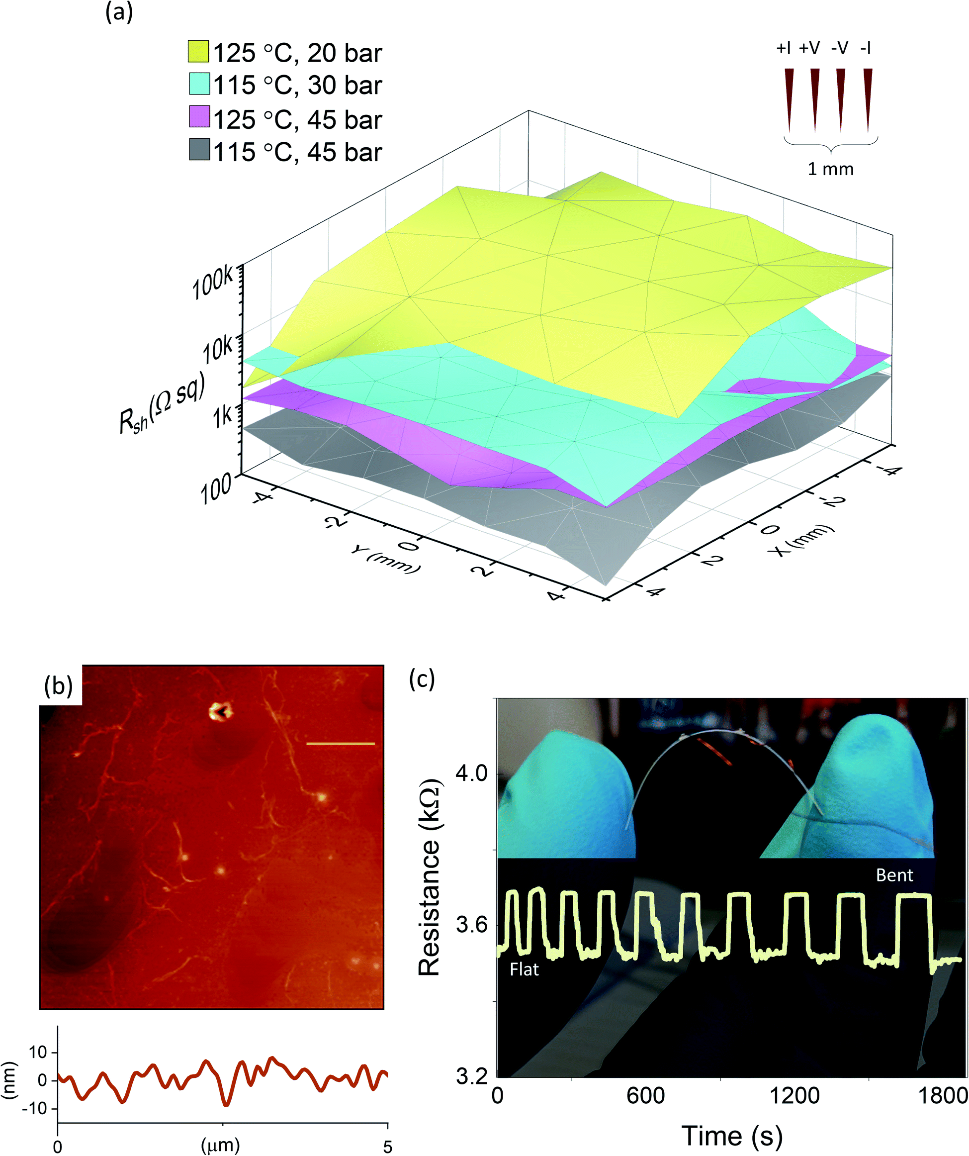 | ||
| Fig. 3 (a) Sheet resistance map for laminated samples at 125 °C, 20 bar (yellow), 115 °C, 30 bar (cyan), 125 °C, 45 bar (pink), 115 °C, 45 bar (grey). (b) Atomic force microscope image of a laminated sample with a line profile over 5 μm (shown in the scale bar). (c) Bending measurements performed on a laminated sample showing measurements under normal and bent conditions. | ||
The lowest sheet resistance we have obtained is 1 kΩsq−1, on a sample that was laminated at 115 °C and 45 bar (sample 9 in Table 1), that conforms well to CVD graphene samples obtained by wet transfer techniques,5,28,29 and indicates that our method could emerge as an alternative to such methods. An atomic force microscopy image of a large area, shown in Fig. 3b reveals laminated graphene with ripples and an average roughness ∼ 3–4 nm with scans over a long distance of 5 μm. To test the stability of the films, we have subjected films to multiple bending cycles, each step lasting an average time ∼100 seconds in both flat and bent conditions. The bending test plot, shown in Fig. 3c, confirms that our laminated graphene films are highly resilient with bending radii as small as 5 mm, similar to our earlier reports on wet transferred graphene5 as well as atomically smooth flexible indium tin oxide (ITO) films.30
We also performed Raman spectroscopy using an excitation radiation of λ = 532 nm on different points in the laminated and non-laminated areas. In Fig. 4a, we show the Raman spectra of the PEN substrate as well as laminated graphene on PEN. Since the signal from PEN masks the graphene G peak,5 we confirmed the presence of graphene by its characteristic 2D peak, which is observed only in the laminated areas. The inset of Fig. 4a shows the Raman spectra in 2D peak region on samples 9, 12, and 15, measured on the PEN region (A), and the laminated graphene region (B). A Lorentzian fitting of the 2D peak for laminated samples reveals an FWHM ∼26 cm−1, expected for single-layer graphene,31 and matches closely to samples obtained by conventional wet transfer process (shown in ESI Fig. S2†).
 | ||
| Fig. 4 (a) Raman spectra measured on a laminated area on several samples (B) and Raman spectra measured on PEN on the non-laminated area (A). The 2D peak of graphene is only visible in the laminated area (B). Inset shows the two different areas on a sample along with Raman peaks in several points in A and B regions. (b) Transmittance as a function of wavelength for different samples. 120 °C 45 bar (black), 115 °C 45 bar (blue), and 125 °C 45 bar (yellow) in the visible spectrum wavelength. (c) Transmittance as a function of wavelength for PEN substrate. (d) Absorbance of graphene laminated on the substrate obtained by deconvoluting substrate contribution (c) from total transmittance (b). | ||
Transparency of flexible substrates is a crucial property for optoelectronic applications. Therefore, to understand the transmission properties of transferred graphene, we have studied the transmission coefficient using a photo-spectrometer [PerkinElmer Ltd. model Lambda 900]. Fig. 4b shows the transmittance of the samples 9, 12, and 15, between 380 nm to 800 nm wavelength range. We observe a percentage transmission of 80% at 400 nm, which saturates for higher wavelengths at a maximum value of 85.5% at 650 nm, similar to wet transferred graphene (see Fig. S3†). Typical ITO based commercial transparent electrodes with 100 nm thick ITO layer display a sheet resistance of 30 Ω sq−1 and transparency ∼85%,32 which indicates that the conducting graphene|PEN sample show optimum transparency for transparent electrode applications. Considering the high PEN substrate transmittance (shown in Fig. 4c) and the total transmittance of laminated graphene samples (Fig. 4b), we obtain a very low absorption ∼2% for graphene, which is expected for high-quality single-layer graphene.33
Sputtered ITO films generally need to be transformed into crystalline form to acquire high transparency, low resistivity, and mechanical stability. Such transformation requires heat treatment at 250 °C, a temperature that cannot be tolerated by flexible substrates. However, it is possible to make flexible ITO films at room temperature through other methods30 with film thicknesses in the range 10–100 nm. Reports also suggest the intermediate graphene support for stability and enhancement in the flexibility of ITO films.32 Despite this, ITO is easily broken under ∼2% strain, while the graphene-based substrate with single-layer graphene intrinsically has a high strain capacity ∼10%.3 Therefore, graphene comes with exceptional flexibility and resilience. In addition to ITO, today, there exist several highly tested methods to produce flexible transparent substrates that include AgNWs, CNTs that provide competitive sheet resistance and transmittance.34 However, considering its atomically thin nature consisting of a single layer of carbon atoms, the volume conductivity in graphene is still high and obtained by a simple process of direct lamination and etching. Therefore, these features suggest tremendous potential and scope for the laminated graphene|PEN samples for future exploration in transparent and flexible electrodes.
In addition to the transfer of the graphene layer, the possibility of embossing patterns of graphene could open up new opportunities for building high-quality graphene circuits. To demonstrate this possibility, we have transferred a graphene pattern onto the flexible substrate using a 3d printed mask. First, the mask was printed out of black isotropic photopolymer resin in a 3d printer [FormLabs model Form2 Stereolithography (SLA)] for a pattern shown in Fig. 5a. The mask was then placed on CVD graphene on Cu substrate for patterning of graphene using oxygen plasma at 50 W power, 45 sccm O2 flow, and 20 torr pressure for 1 minute [Reactive Ion Etching tool model Advanced Vacuum Vison 320]. Graphene is etched out in the first places where the mask exhibits holes. Following this, the Cu foil containing the rest of the graphene was laminated onto a PEN substrate using the optimized conditions that we described (125 °C and 45 bar). In Fig. 5b, a patterned graphene sheet laminated onto the flexible substrate is displayed. The Raman spectra of the graphene region and bare PEN region are presented in Fig. 5c. We perform sheet resistance in several points of the sample that yielded a sheet resistance ∼4 kΩ sq−1, which is a reasonable value considering the net coverage of the patterned graphene, and the expected value for CVD graphene.28,29
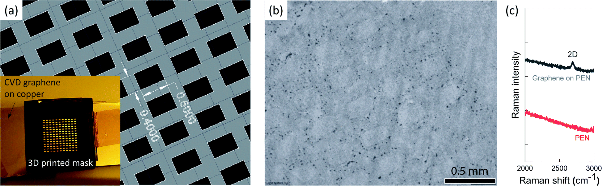 | ||
| Fig. 5 (a) Pattern of mask for 3D printing. Inset: 3D printed mask on initial CVD graphene containing copper foil. (b) Microscope image of the patterned graphene with a 3d printed mask. (c) Raman spectra of graphene region and bare PEN region after lamination. | ||
Since graphene was first isolated 15 years ago, there still exists a need for concrete techniques for direct graphene lamination onto flexible substrates, which can make processing flexible graphene sheets economical while enhancing application potential. Our experiments here give a first proof-of-principle demonstration of direct lamination of large-scale CVD graphene onto technologically prospective PEN substrates without any intermediate layer. Despite the recent approaches using roll-to-roll lamination or direct lamination with an adhesive layer, the common transfer technique for large-scale applications such as screens is still wet transfer technique.35 Nanoimprint lamination method is, in principle, a scalable method and a new way to laminate graphene electrodes with a reasonable sheet resistance in two steps (lamination and etching), with additional capability for patterned transfer. It is of great importance for the commercialization of flexible graphene systems as transparent electrodes and electrode material for flexible batteries and capacitors etc. At the same time, the technique that we presented here is open to improvements in each step of processing and fabrication. Furthermore, a new prospect could be to try multiple transfers of graphene and other graphene-like crystals.
4 Conclusions
To summarize, we demonstrated a direct-transfer method of scalable graphene transfer onto a flexible PEN substrate without the need for any intermediate layer. By large-scale characterization using electrical, optical, and Raman spectroscopy, we investigated the properties of the transferred graphene. By controlling the temperature and pressure of the lamination process, it is possible to obtain direct transfer that shows standard sheet resistance ∼ 1 kΩ of competitive quality, a high optical transmittance up to 85%, added by high resilience of the graphene flexible films. Furthermore, by this process, it is possible to transfer pre-patterned graphene sheets onto flexible PEN substrates using 3d printed masks. Achieved at a reasonably low temperature and time-scale of a few hours, our technique opens for scalable production of flexible graphene system. Our work shows the promise of a direct laminated graphene for creating transparent, flexible, patterned graphene electrodes, and a flexible conducting platform for many electronic and optoelectronic applications.Conflicts of interest
There are no conflicts to declare.Acknowledgements
MVK thanks the support of FORMAS Grant no. 2019-01326, VR starting Grant (2016-03278) from the Swedish Research Council, Stiftelsen Olle Engkvist Byggmästare (200-0602), and Wenner-Gren Stiftelserna (UPD2018-0057). The authors thank Himanshu Mishra and Ramu Maddu for their assistance during the revision stage.References
- K. S. Novoselov, D. Jiang, F. Schedin, T. J. Booth, V. V. Khotkevich, S. V. Morozov and A. K. Geim, Proc. Natl. Acad. Sci. U. S. A., 2005, 102, 10451 CrossRef CAS PubMed.
- F. Bonaccorso, Z. Sun, T. Hasan and A. C. Ferrari, Nat. Photonics, 2010, 4, 611 CrossRef CAS.
- S. Bae, H. Kim, Y. Lee, X. Xu, J.-S. Park, Y. Zheng, J. Balakrishnan, T. Lei, H. Ri Kim, Y. Il Song, Y.-J. Kim, K. S. Kim, B. Özyilmaz, J.-H. Ahn, B. H. Hong and S. Iijima, Nat. Nanotechnol., 2010, 5, 574 CrossRef CAS PubMed.
- K. S. K. S. K. S. Kim, Y. Zhao, H. Jang, S. Y. S. Y. Lee, J. M. J. M. Kim, J. J.-H. J.-H. Ahn, P. Kim, J.-Y. J.-Y. Choi, B. H. B. H. Hong, K. S. K. S. K. S. Kim, J. J.-H. J.-H. Ahn, P. Kim, J.-Y. J.-Y. Choi and B. H. B. H. Hong, Nature, 2009, 457, 706 CrossRef CAS PubMed.
- I. G. Serrano, J. Panda, F. Denoel, Ö. Vallin, D. Phuyal, O. Karis and M. V. Kamalakar, Nano Lett., 2019, 19, 666 CrossRef CAS PubMed.
- F. Godel, M. V. Kamalakar, B. Doudin, Y. Henry, D. Halley and J.-F. Dayen, Appl. Phys. Lett., 2014, 105, 152407 CrossRef.
- J.-F. Dayen, S. J. Ray, O. Karis, I. J. Vera-Marun and M. V. Kamalakar, Appl. Phys. Rev., 2020, 7, 011303 Search PubMed.
- N. Petrone, J. Hone and D. Akinwande, Nat. Commun., 2015, 5, 1 Search PubMed.
- H. Xin and W. Li, Appl. Phys. Rev., 2018, 5, 031105 Search PubMed.
- V. B. Timofeev, V. I. Popov, D. V. Nikolaev, T. E. Timofeeva and S. A. Smagulova, Nanotechnol. Russ., 2017, 12, 62 CrossRef CAS.
- Q. Yu, J. Lian, S. Siriponglert, H. Li, Y. P. Chen and S.-S. Pei, Appl. Phys. Lett., 2008, 93, 113103 CrossRef.
- X. Li, Y. Zhu, W. Cai, M. Borysiak, B. Han, D. Chen, R. D. Piner, L. Colomba and R. S. Ruoff, Nano Lett., 2009, 9, 4359 CrossRef CAS PubMed.
- X. Li, W. Cai, J. An, S. Kim, J. Nah, D. Yang, R. Piner, A. Velamakanni, I. Jung, E. Tutuc, S. K. Banerjee, L. Colombo and R. S. Ruoff, Science, 2009, 324, 1312 CrossRef CAS PubMed.
- A. Pirkle, J. Chan, A. Venugopal, D. Hinojos, C. W. Magnuson, S. McDonnell, L. Colombo, E. M. Vogel, R. S. Ruoff and R. M. Wallace, Appl. Phys. Lett., 2011, 99, 2009 CrossRef.
- A. E. Islam, D. N. Zakharov, J. Carpena-Nuňez, M. S. Hsiao, L. F. Drummy, E. A. Stach and B. Maruyama, Appl. Phys. Lett., 2017, 111, 103101 CrossRef.
- J. W. Suk, W. H. Lee, J. Lee, H. Chou, R. D. Piner, Y. Hao, D. Akinwande and R. S. Ruoff, Nano Lett., 2013, 13, 1462 CrossRef CAS PubMed.
- H. Park, C. Lim, C. J. Lee, J. Kang, J. Kim, M. Choi and H. Park, Nanotechnology, 2018, 29, 415303 CrossRef PubMed.
- L. G. P. Martins, Y. Song, T. Zeng, M. S. Dresselhaus, J. Kong and P. T. Araujo, Proc. Natl. Acad. Sci. U. S. A., 2013, 110, 17762 CrossRef CAS PubMed.
- H. Park, P. R. Brown, V. Bulović and J. Kong, Nano Lett., 2012, 12, 133 CrossRef CAS PubMed.
- C. S. Chen and C. K. Hsieh, Thin Solid Films, 2014, 570, 595 CrossRef CAS.
- G. H. Han, H.-J. Shin, E. S. Kim, S. J. Chae, J.-Y. Choi and Y. H. Lee, Nano, 2011, 06, 59 CrossRef CAS.
- V. P. Verma, S. Das, I. Lahiri and W. Choi, Appl. Phys. Lett., 2010, 96, 203108 CrossRef.
- W. A. MacDonald, in Large Area Flex. Electron, Wiley-VCH Verlag GmbH & Co. KGaA, Weinheim, Germany, 2015, pp. 291–314 Search PubMed.
- S. Y. Chou, P. R. Krauss and P. J. Renstrom, Science, 1996, 272, 85 CrossRef CAS.
- A. Pietrikova, P. Lukacs, D. Jakubeczyova, B. Ballokova, J. Potencki, G. Tomaszewski, J. Pekarek, K. Prikrylova and M. Fides, Circuit World, 2016, 42, 9 CrossRef.
- M. Chen, R. C. Haddon, R. Yan and E. Bekyarova, Mater. Horiz., 2017, 4, 1054–1063 RSC.
- G. Z. Papageorgiou, V. Tsanaktsis and D. N. Bikiaris, Phys. Chem. Chem. Phys., 2014, 16, 7946 RSC.
- A. Mahmood, C.-S. S. Yang, J.-F. F. Dayen, S. Park, M. V. Kamalakar, D. Metten, S. Berciaud, J. O. Lee and B. Doudin, Carbon, 2015, 86, 256 CrossRef CAS.
- M. V. Kamalakar, C. Groenveld, A. Dankert and S. P. Dash, Nat. Commun., 2015, 6, 6766 CrossRef CAS PubMed.
- J. H. Kim, H. J. Seok, H. J. Seo, T. Y. Seong, J. H. Heo, S. H. Lim, K. J. Ahn and H. K. Kim, Nanoscale, 2018, 10, 20587 RSC.
- J. S. Park, A. Reina, R. Saito, J. Kong, G. Dresselhaus and M. S. Dresselhaus, Carbon, 2009, 47, 1303 CrossRef CAS.
- S. J. Lee, Y. Kim, J.-Y. Hwang, J.-H. Lee, S. Jung, H. Park, S. Cho, S. Nahm, W. S. Yang, H. Kim and S. H. Han, Sci. Rep., 2017, 7, 3131 CrossRef PubMed.
- R. R. Nair, P. Blake, A. N. Grigorenko, K. S. Novoselov, T. J. Booth, T. Stauber, N. M. R. Peres and A. K. Geim, Science, 2008, 320, 1308 CrossRef CAS PubMed.
- Y. Zhu, Y. Deng, P. Yi, L. Peng, X. Lai and Z. Lin, Adv. Mater. Technol., 2019, 4, 1 Search PubMed.
- J.-W. Shin, J.-H. Han, H. Cho, J. Moon, B.-H. Kwon, S. Cho, T. Yoon, T.-S. Kim, M. Suemitsu, J.-I. Lee and N. S. Cho, 2D Mater., 2017, 5, 014003 CrossRef.
Footnote |
| † Electronic supplementary information (ESI) available. See DOI: 10.1039/d0na00046a |
| This journal is © The Royal Society of Chemistry 2020 |