
 Open Access Article
 This Open Access Article is licensed under a
 Creative Commons Attribution 3.0 Unported Licence
Progress in lead-free piezoelectric nanofiller materials and related composite nanogenerator devices
Yong
Zhang
ab,
Hyunseung
Kim
c,
Qing
Wang
 d,
Wook
Jo
e,
Angus I.
Kingon
f,
Seung-Hyun
Kim
*f and
Chang Kyu
Jeong
*cg
d,
Wook
Jo
e,
Angus I.
Kingon
f,
Seung-Hyun
Kim
*f and
Chang Kyu
Jeong
*cg
aState Key Laboratory of Silicate Materials for Architectures, Center for Smart Materials and Device Integration, School of Materials Science and Engineering, Wuhan University of Technology, Wuhan 430070, China
bDepartment of Materials Science and Engineering, National University of Singapore, 9 Engineering Drive 1, 117575, Singapore
cHydrogen and Fuel Cell Research Center, Department of Energy Storage/Conversion Engineering, Jeonbuk National University, Jeonju, Jeonbuk 54896, Republic of Korea. E-mail: ckyu@jbnu.ac.kr
dDepartment of Materials Science and Engineering, The Pennsylvania State University, University Park, PA 16802, USA
eSchool of Materials Science and Engineering, Jülich-UNIST Joint Leading Institute for Advanced Energy Research (JULIA), Ulsan National Institute of Science and Technology (UNIST), Ulsan 44919, Republic of Korea
fSchool of Engineering, Brown University, Providence, RI 02912, USA. E-mail: seunghyun_kim@brown.edu
gDivision of Advanced Materials Engineering, Jeonbuk National University, Jeonju, Jeonbuk 54896, Republic of Korea. E-mail: ckyu@jbnu.ac.kr
First published on 29th April 2020
Abstract
Current piezoelectric device systems need a significant reduction in size and weight so that electronic modules of increasing capacity and functionality can be incorporated into a great range of applications, particularly in energy device platforms. The key question for most applications is whether they can compete in the race of down-scaling and an easy integration with highly adaptable properties into various system technologies such as nano-electro-mechanical systems (NEMS). Piezoelectric NEMS have potential to offer access to a parameter space for sensing, actuating, and powering, which is inflential and intriguing. Fortunately, recent advances in modelling, synthesis, and characterization techniques are spurring unprecedented developments in a new field of piezoelectric nano-materials and devices. While the need for looking more closely at the piezoelectric nano-materials is driven by the relentless drive of miniaturization, there is an additional motivation: the piezoelectric materials, which are showing the largest electromechanical responses, are currently toxic lead (Pb)-based perovskite materials (such as the ubiquitous Pb(Zr,Ti)O3, PZT). This is important, as there is strong legislative and moral push to remove toxic lead compounds from commercial products. By far, the lack of viable alternatives has led to continuing exemptions to allow their temporary use in piezoelectric applications. However, the present exemption will expire soon, and the concurrent improvement of lead-free piezoelectric materials has led to the possibility that no new exemption will be granted. In this paper, the universal approaches and recent progresses in the field of lead-free piezoelectric nano-materials, initially focusing on hybrid composite materials as well as individual nanoparticles, and related energy harvesting devices are systematically elaborated. The paper begins with a short introduction to the properties of interest in various piezoelectric nanomaterials and a brief description of the current state-of-the-art for lead-free piezoelectric nanostructured materials. We then describe several key methodologies for the synthesis of nanostructure materials including nanoparticles, followed by the discussion on the critical current and emerging applications in detail.
 Yong Zhang | Dr Yong Zhang is a professor of School of Materials Science and Engineering at Wuhan University of Technology (WUT). He received his Ph.D. degree (2018) in Materials Science and Engineering from WUT. He was a visiting student at The Pennsylvania State University from 2015 to 2017. His research interests include ferroelectric ceramics, polymer-based composites, and new nanomaterials for energy storage and conversion. |
 Qing Wang | Dr Qing Wang is a Professor of Materials Science and Engineering at the Pennsylvania State University, University Park, PA. He received his Ph.D. in Chemistry from the University of Chicago in 2000. Prior to joining the faculty at Penn State in 2002, he was a postdoctoral researcher at Cornell University. His research interests include the development of ferroelectric polymers, electroactive polymers and polymer nanocomposites for energy harvesting and storage. |
 Wook Jo | Dr Wook Jo is a head of Jülich-UNIST joint Leading Institute for Advanced energy research (JULIA) and a professor at the School of Materials Science and Engineering, Ulsan National Institute of Science and Technology (UNIST), South Korea. His research has focused on the functional properties of ferroelectric materials with a special emphasis on lead-free piezoceramics and relaxor ferroelectrics. Recently, he is actively contributing to the field of high temperature dielectrics and room temperature multiferroics. He has published more than 150 refereed journal papers, seven books, and holds six patents. |
 Angus I. Kingon | Dr Angus Kingon obtained his B.Sc. (Hons) from the University of the Witwatersrand and then the M.Sc (cum laude) and Ph.D. degrees from the University of South Africa while working at the Council for Scientific and Industrial Research in South Africa. He joined the faculty of the Department of Materials Science and Engineering at North Carolina State University in 1987. Since 2008, he has been at Brown University, as Professor of Engineering and University Professor of Entrepreneurship and Organizational Studies. He has published about 340 papers, edited 7 books, published 6 book chapters, and has 23 issued patents. |
 Seung-Hyun Kim | Dr Seung-Hyun Kim is a professor in School of Engineering at Brown University. Prior to joining Brown, he was a senior executive vice president of MEMS related company and was the head of Research and Development Center. He has been active in ferroelectric, dielectric and piezoelectric thin films for electronic devices for the last 30 years. Prof. Kim's research interests are in the area of the development of piezoelectric and energy devices and MEMS processing. Prof. Kim's educational and academic activities cover experimentation and applications of small-scale electronic materials and devices. |
 Chang Kyu Jeong | Dr Chang Kyu Jeong is currently a professor in Jeonbuk National University, Korea (note that the previous name is Chonbuk National University). He received his B.S. degree in Materials Science and Engineering from Hanyang University and M.S./Ph.D. degrees from Korea Advanced Institute of Science and Technology (KAIST), respectively. After working on a postdoctoral research fellow at Institute for NanoCentury, he was employed as a postdoctoral scholar at Pennsylvania State University. His current research topics are ferroelectric/piezoelectric materials, biological/biomimetic electronic materials and devices, and other electromechanical coupling phenomena (flexoelectric, ferroelectret, ionic migration, electrostatic, etc.) for energy and sensor applications. |
1. Introduction
The piezoelectric effect, which was first identified by Jacques and Pierre Curie in 1880, offers near instantaneous conversion of electromechanical energy with extreme precision and is thus utilized in many applications such as accelerometers, actuators, fuel injectors, motors, resonators, sensors, transducers and energy harvester, etc.1–4 In general, piezoelectric materials are simply divided into four categories: ceramics, polymers, single crystals, and organic–inorganic hybrid composites. Among them, piezoelectric ceramics have gained a huge popularity in the global market due to high piezoelectric performances and electromechanical conversion efficiencies, easy morphology- and property-tunability, low manufacturing cost, and easy mass production.5,6 So far, piezoelectrics have been traditionally dominated by Pb(Zr,Ti)O3 (PZT), which contains ∼60 wt% of environmentally hazardous lead.7,8 In several countries, including European Union (EU) and the U.S. state California, the directive Restriction on the Use of Certain Hazardous Substances in Electrical and Electronic Equipment (RoHS II) or an equivalent has been implemented in the legislation.9 According to the regulations, the concentration of lead in homogeneous material in the household or industrial devices must not exceed 0.1 wt%.3 Piezoelectrics for particular applications have been granted an exemption until a feasible alternative for lead-based materials are ready for use.10,11 This caused a huge burst in the research of lead-free piezoelectric materials in the last 30 years. Even if there are no viable lead-free piezoelectric material alternatives yet, recent encouraging results have demonstrated that some of the lead-free piezoelectric ceramic materials are beginning to approach PZT in performance.12–15 In addition to piezoelectric bulk ceramic materials, the usage of lead-based piezoelectric nanofillers including nanoparticles for hybrid composites has also suffered from the strict inspection due to toxicity of lead and is expected to have the same restriction in the near future, implying an urgent and emerging need for finding eco-friendly lead-free nanomaterial alternatives. Therefore, an insight-driven and massively parallel research trend of eco-friendly and size-scaled material systems has been expanded to nanoscience and nanotechnology. Specifically, perovskite-type piezoelectric nanostructured materials have attracted great interests due to their potential properties – including size, shape, optical and thermal responses, and dielectric and piezoelectric characteristics, which can be controlled by external forces such as electric field and physical stimulus representatively pressure, though not limited to pressure, strain/stress, vibration, and torsion etc. One of most important features is that these piezoelectric nanostructure materials can generate a factor of four to six increase in the extrinsic piezoelectric response compared to polycrystalline thin films.Stretching our collective investigations to take a full advantage of nanoscale devices (e.g., nano-electro-mechanical systems (NEMS), nanogenerators, etc.) demand the exploration of novel transduction mechanism, fundamental understanding of nanostructure materials, fabrication of nanoscale materials and devices, and future perspectives.16–18 Piezoelectric nanomaterials (PNs) are generally classified into several categories based on a diverse range of configurations and dimensions, i.e., zero-dimensional (0D) PNs (nanoparticles and nanocubes), one-dimensional (1D) PNs (nanowires, nanofibers, nanorods and nanotubes) and two-dimensional (2D) PNs (nanoplates and nanofilms).19 Isotropic 0D nanoparticles with various sizes represent the most common nanoscale configuration for current massive applications and commercial products due to relatively simple synthesis flow and high-yield and high-quality manufacturing.20 These PNs with stringent process and quality controls have laid the foundation of a myriad of piezoelectric NEMS applications such as nanoactutors, nanosensors, nanoprobes, nanoresonators and nanogenerators, etc.21 In particular, nanogenerators, which were initially proposed by Z. L. Wang's research group in 2006, have become one of the hottest topics in materials and energy related research community.22 Piezoelectric nanogenerators are defined as mechanical energy harvesting devices with promising abilities for harvesting random mechanical energy into electric energy by utilizing piezoelectric effect or other electromechanical coupling phenomena.23,24 They have demonstrated high potentials for driving small-scale and low power electronics, wireless sensor networks, and implantable biomedical devices with self-powering capability.25–31 While a significant headway has been made in the field of nanogenerators, the amount of energy produced in most cases is still not sufficient to power the desired electronic systems. Therefore, a number of research strategies (through optimal selections of high-performance piezoelectric materials, ordered arrangement of materials, device structures, theoretical simulations, etc.) have been proposed and performed to improve the overall output power of piezoelectric energy harvesters, which will be summarized in the following sections.32–34
As described above, lead-free piezoelectric nanomaterials and related energy harvesting devices have attracted great attention with recent burgeoning advances.35 Although the vast majority of piezoelectric materials are mainly perovskite and wurtzite structures,36–39 the importance of piezoelectric phenomena has triggered a broad search for other non-traditional piezoelectric material systems such as 2D materials (e.g., hexagonal boron nitrate (h-BN) and molybdenum disulfide (MoS2))40,41 and biomaterials (elastin, virus, spider silk, etc.)42,43 for unprecedented levels of new piezoelectric properties.44–47 It is important to note that the underlying physics in and related electromechanical coupling mechanisms for such new material systems, which are complex and not fully understood, need to be clarified further through more systematic investigations to enhance our understanding in this research field.48
Even though there have been a number of reviews on lead-free piezoelectric nanomaterials due to high potentials for future eco-friendly and biocompatible electronic applications,11,49,50 the understanding and the control of piezoelectric material properties at nanometer-scale are still at a very basic level, with the majority of reports just focusing on overcoming the processing difficulties. In addition, a fundamental understanding of the size effects on the functional piezoelectric response is still needed since limited knowledge exists on the origins of the performance of and the mechanisms for piezoelectric nanomaterials and devices due to the complex nature of materials and difficulty in fabrication at nanoscales. Moreover, the extensive research on this field during the last several years has intrigued new phenomena through recent advances in modelling, synthesis and characterization techniques, which have not been included in the previous reviews to date. Thus, this review article explores how the study of piezoelectric nanomaterials, specifically nanoparticles and nano-composites, has expanded our understanding of fundamental effects, enabled the discovery of novel phases and physics, and allowed unprecedented control of properties. This review also discusses several exciting possibilities for the development of new materials and devices, including those in transduction sensors and energy harvesting devices. This article provides a comprehensive overview and summary of the investigations on the universal approaches to and recent progresses of lead-free piezoelectric nanoparticles and related energy harvesting devices. We believe that this review can be an excellent research training vehicle, as it demands both research depth and breadth, and covers multidisciplinary topics ranging from fundamental studies of nanoscale piezoelectric materials, and process optimization to advanced application aspects such as device structures, fabrication methodologies, and design elements of energy harvesting devices (nanogenerators). It provides the researchers with knowledge and awareness of scale issues of the functional structure in current miniaturized electronic devices where the size is receiving increasing attention. It should be noted that various shapes of lead-free piezoelectric nanomaterials such as nanowires, nanorods and nanosheets are considered as nanoparticles in this review, because they can be regarded as 1D or 2D nanoparticles in general.51 Finally, this paper highlights future challenges and perspectives for successful implementation of piezoelectric nanomaterials in energy harvesting device applications in the last part. It is expected to yield key insights into the science of the phenomenon, including resolving the current issues regarding scaling effects and practical device applications. We hope that this comprehensive review would provide a timely update and a valuable guidance for the scientists and engineers who are working in the field of piezoelectric nanomaterials and related energy devices.
2. Lead-free piezoelectric nanomaterials
2.1 Types of lead-free piezoelectric nanomaterials
Lead-free piezoelectric nanomaterials could be simply divided into several groups according to their crystal configuration: perovskite structure, wurtzite structure, and new material systems. In this paper, the new systems (i.e. 2D materials) are typically defined as diverse compositions which cannot be affiliated with perovskite and wurtzite structures. We will summarize them one by one from the lesson of brief history to the currently studied level. Note that the piezoelectricity of bismuth-layered structures (e.g. Bi4Ti3O12) and tungsten bronze structures (e.g. KSr2Nb5O15) are not within the scope of this review because the two material families have been mainly identified in bulk materials.52 | ||
| Fig. 1 Stereoscopic illustration of ABO3 perovskite structures (a) with centrosymmetry and (b) with non-centrosymmetry by B ions upwards or downwards. (c) Schematics of wurtzite structure (ZnO as an example) and the related piezoelectric effect. This figure has been adapted/reproduced from ref. 53 with permission from John Wiley & Sons, copyright 2016. | ||
Table 1 lists the mainstream perovskite piezoelectric compounds with a general molecular formula of ABO3 and the molecular ferroelectrics with a general chemical formula of ABO3 and the organic–inorganic hybrid ferroelectrics with a general chemical formula of ABX3 (X means halogen elements). To clearly summarize our discussion below, we intentionally group the ABO3 into three categories: AIBVO3, AIIBIVO3 and AIIIBIIIO3. The superscript roman numerals stand for the valence state of corresponding cations. The construction of solid solutions among these three (e.g. BiFeO3–BaTiO3, BiScO3–PbTiO3, (Na,Bi)TiO3–BaTiO3, (Bi,Na)TiO3-(Bi,K)TiO3–BaTiO3, etc.) are also possible with the mixed valence states on both A and B sites.54–60 As well demonstrated in the previous studies, the construction of solid solutions is a universal and effective approach to high-performance dielectric, piezoelectric, ferroelectric and/or relaxor properties with the modification of phase types, defect chemistry or microstructrues.61–63 For example, Lee et al. reported a bismuth ferrite and barium titanate solid solution compound, which presents good piezoelectric properties (d33 = 402 pC N−1) and a high Curie temperature (Tc = 454 °C).64 The fundamental origin of improved piezoelectric response basically lies in the flattened free energy landscape, causing the ferroelectric polarization to rotate more easily.
| Structure | Compositions |
|---|---|
| AIBVO3 | LiNbO3, KNbO3, NaNbO3, (K,Na)NbO3, etc. |
| AIIBIVO3 | BaTiO3, PbZrO3, PbTiO3, (Na,Bi)TiO3, Pb(Zr,Ti)O3, ZnSnO3, etc. |
| AIIIBIIIO3 | BiFeO3, BiScO3, etc. |
| ABX3 | Me3NCH2ClMnCl3, Me3NCH2ClCdCl3, etc. |
(i) AIBVO3. As a typical AIBVO3 perovskite ferroelectrics, (K0.5Na0.5)NbO3 (KNN) system is characterized by a high Curie temperature (Tc = 420 °C), good ferroelectric properties (Pr = 33 μC cm−2), and large electromechanical coupling factors, which is powerfully considered as one of the most promising lead-free piezoelectric ceramic materials and suitable for environmental and biological compatibility.65–68 Pristine KNN undergoes phase transitions from a paraelectric phase (cubic) to ferroelectric phases (tetragonal, orthorhombic and rhombohedral), and typically presents an orthorhombic symmetry at room temperature.69 Among various lead-free piezoelectric ceramic compounds, the KNN system have attracted most attention from the research community not only to macroscale bulk materials but also to nanoscale materials. Nanostructures with various morphologies, (e.g. nanoparticles, nanocubes, nanowires, nanofibers, nanoplates, nanofilms, etc.) have been demonstrated by various physical and wet chemical methods.70–72 0D (nanocubes) and 1D (nanorods) KNN nanostructures are shown in Fig. 2a and b.70,73 Note that more detailed fabrication procedures and morphology modulation will be discussed in Section 2.2.
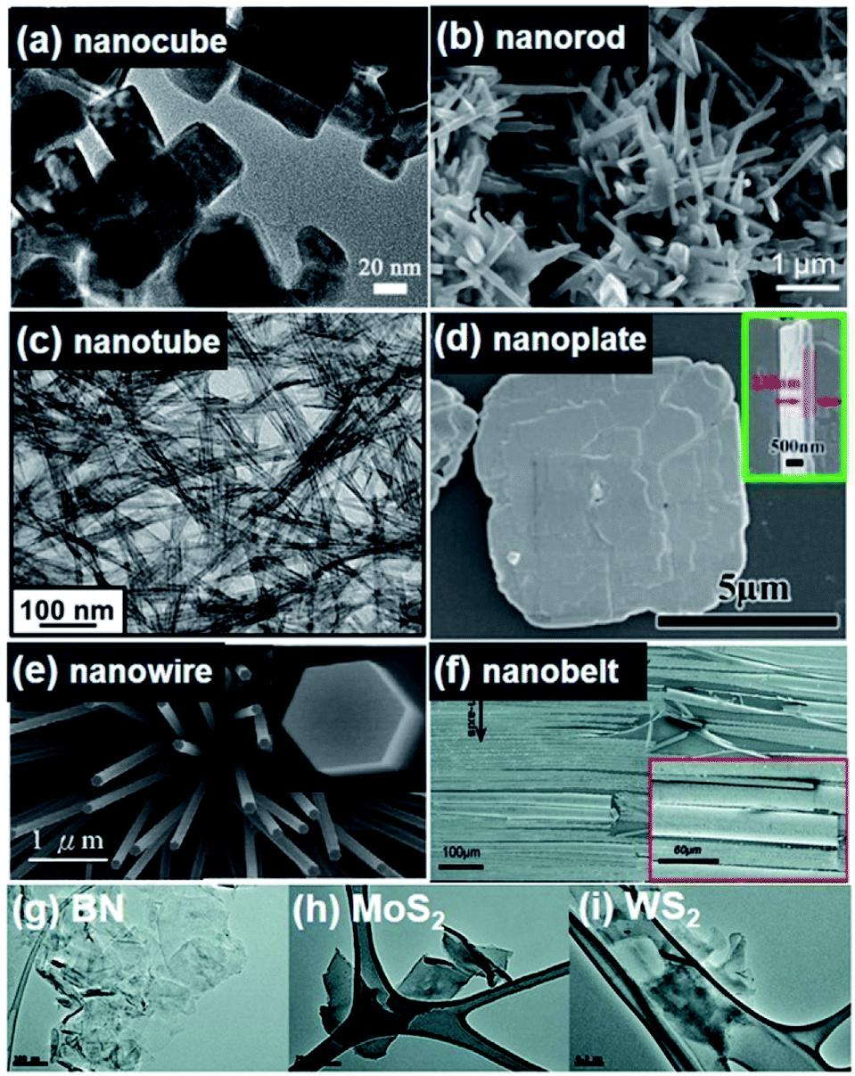 | ||
| Fig. 2 All figures are scanning electron microscopy (SEM) images. (a) (K0.5Na0.5)NbO3 nanocube synthesized by a combustion process using polyacrylic acid (PAA) as a fuel. (b) (K0.99Na0.01)NbO3 nanorods fabricated by a hydrothermal method. (c) BaTiO3 nanotubes obtained by a hydrothermal approach. (d) BiFeO3 nanoplates synthesized by a hydrothermal approach. (e) Grown ZnO nanowires. (f) GaN nanobelts. (g–i) mechanically exfoliated monolayer of 2D BN, MoS2 and WS2, respectively. This figure has been adapted/reproduced from ref. 18, 70, 82 and 95–98 with permission from Elsevier, copyright 2016; Elsevier, copyright 2015; American Chemical Society, copyright 2012; American Chemical Society, copyright 2018; Royal Chemical Society, copyright 2020; IOP Science, copyright 2008; and John Wiley & Sons, copyright 2012, respectively. | ||
(ii) AIIBIVO3. In 1940's, the piezoelectricity of artificially synthesized polycrystalline materials was firstly demonstrated in BaTiO3 ferroelectric ceramics. Although it is mainly used as a dielectric material for multi-layered ceramic capacitors (MLCC) nowadays due to its excellent dielectric properties, more and more studies using BaTiO3 as a model material to investigate the nanoscale effect of ferroelectrics and piezoelectrics.18,74 Pristine BaTiO3 undergoes a series of first-order phase transitions as follows: cubic (Pm
![[3 with combining macron]](https://www.rsc.org/images/entities/char_0033_0304.gif) m) to tetragonal (P4mm), to orthorhombic (Amm2), and then to rhombohedral (R3m) during cooling from high temperatures.59,75 As well studied, the construction of morphotropic phase boundary (MPB) or polymorphic phase boundary (PPB) at room temperature was considered as an efficient strategy for higher piezoelectric responses of BaTiO3-based ceramics. In 2009, the potential of BaTiO3-based materials was renewed for high-performance piezoelectric applications as reporting an extremely high piezoelectric coefficient (d33 ∼ 620 pC N−1) at a composition in Ba(Ti0.8Zr0.2)O3–(Ba0.7Ca0.3)TiO3.76 Note that the piezoelectricity of nanomaterials may be different from their bulk counterparts due to the existence of surface and size effect.77 Nevertheless, syntheses and uses of nanomaterials largely and inevitably follow the trend of bulk ceramics. Thus, BaTiO3-based nanomaterials, especially Ba(Ti0.8Zr0.2)O3–(Ba0.7Ca0.3)TiO3, with various morphologies have been examined by sol–gel process,78 supercritical fluids technology,79 solvothermal synthesis,80 molten salt approach,81 and extensively used for lead-free energy and sensor devices since 2009. More details of fabrication and morphology modulation approaches will also be discussed in the subsequent section. Fig. 2c shows the morphology of hydrothermally synthesized BaTiO3 nanotubes with 11.8 (±2.3) nm in diameter and 4.1 (±1.2) μm in length.82
m) to tetragonal (P4mm), to orthorhombic (Amm2), and then to rhombohedral (R3m) during cooling from high temperatures.59,75 As well studied, the construction of morphotropic phase boundary (MPB) or polymorphic phase boundary (PPB) at room temperature was considered as an efficient strategy for higher piezoelectric responses of BaTiO3-based ceramics. In 2009, the potential of BaTiO3-based materials was renewed for high-performance piezoelectric applications as reporting an extremely high piezoelectric coefficient (d33 ∼ 620 pC N−1) at a composition in Ba(Ti0.8Zr0.2)O3–(Ba0.7Ca0.3)TiO3.76 Note that the piezoelectricity of nanomaterials may be different from their bulk counterparts due to the existence of surface and size effect.77 Nevertheless, syntheses and uses of nanomaterials largely and inevitably follow the trend of bulk ceramics. Thus, BaTiO3-based nanomaterials, especially Ba(Ti0.8Zr0.2)O3–(Ba0.7Ca0.3)TiO3, with various morphologies have been examined by sol–gel process,78 supercritical fluids technology,79 solvothermal synthesis,80 molten salt approach,81 and extensively used for lead-free energy and sensor devices since 2009. More details of fabrication and morphology modulation approaches will also be discussed in the subsequent section. Fig. 2c shows the morphology of hydrothermally synthesized BaTiO3 nanotubes with 11.8 (±2.3) nm in diameter and 4.1 (±1.2) μm in length.82
Even though these types of perovskite piezoelectric ceramics are the simplest composition and the most-friendly material to common engineers, the controls of yield and morphology of 1D type (i.e. nanowires) were considered as highly difficult problems.83 In recent years, however, the scalable synthesis as well as the ultra-long morphology have been developed through the modulated chemistry.84–87
(Na1/2Bi1/2)TiO3 (NBT or BNT), another promising candidate for lead-free piezoelectric materials, was firstly released in 1960.88,89 It possesses a perovskite structure at room temperature with a sequence of phase transitions from cubic to tetragonal to rhombohedral at temperatures of ∼540 °C and ∼300 °C, respectively.90 NBT system shows strong ferroelectric properties with a large remnant polarization (Pr = 38 μC cm−2) and a high Curie temperature (Tc = 320 °C). Moreover, there are notable lead-free relaxor ferroelectric ceramics in the NBT-based compositions for high-performance lead-free piezoelectric devices.91–94 However, it has been limited for many applications due to its relatively large leakage current and low depolarization temperature (Td). Nonetheless, there have been many efforts to overcome the disadvantages of NBT systems. In Table 2, we give several typical references related with nanostructures of NBT and its solid solutions with other perovskite systems such as 0.94(Na1/2Bi1/2)TiO3–0.06BaTiO3.
| Approaches | Composition (with references) | Size (nm) | MP* |
|---|---|---|---|
| a Note: MP*, ME**, CE*** are the abbreviations of morphology, mechanical exfoliating, and chemical exfoliating process, respectively. The blank means various or vague feature at each research. | |||
| Solid-state | (K0.44+xNa0.52Li0.04)(Nb0.86Ta0.10Sb0.04)O3 (ref. 126) | 50–200 | NP |
| Solid-state | BaTiO3 (ref. 157) | 28–105 | NP |
| Solid-state | ZnO (ref. 158) | NP | |
| Solid-state | (K0.44+xNa0.52Li0.04)(Nb0.86Ta0.10Sb0.04)O3 (ref. 126) | 50–200 | NP |
| Solid-state | 0.5Ba(Zr0.2Ti0.8)O3-0.5(Ba0.7Ca0.3)TiO3 (ref. 159) | ∼500 | NP |
| Sol–gel | 0.5Ba(Zr0.2Ti0.8)O3-0.5(Ba0.7Ca0.3)TiO3 (ref. 160) | 30–60 | NP |
| Sol–gel | (1−x)(K0.5Na0.5)NbO3–xLiNbO3 (ref. 129) | 20–30 | NP |
| Sol–gel | (Na0.5Bi0.5)TiO3–BaTiO3 (ref. 161) | NP | |
| Sol–gel | BiFeO3 (ref. 162) | NP | |
| Sol–gel | ZnO (ref. 163) | 18–21 | NP |
| Hydrothermal | BaTiO3 (ref. 164) | NP | |
| Hydrothermal | Na0.5Bi0.5TiO3 (ref. 165) | NP | |
| Hydrothermal | BiFeO3 (ref. 166) | NR | |
| Solvothermal | BaTiO3 (ref. 167) | 80–100 | NP |
| Molten salt | Na0.9K0.1NbO3 (ref. 168) | ∼40 | NP |
| Molten salt | BaTiO3 (ref. 169) | ||
| Molten salt | (K0.5Na0.5)NbO3 (ref. 65) | NR | |
| Supercritical fluid | BaTiO3 (ref. 79) | ||
| Supercritical fluid | BaTi1–yZryO3![[thin space (1/6-em)]](https://www.rsc.org/images/entities/char_2009.gif) (0 ≤ y ≤ 1) (ref. 142) (0 ≤ y ≤ 1) (ref. 142) |
10–25 | NP |
| Electrospinning | V–ZnO (ref. 170) | NF | |
| Electrospinning | (Na0.5Bi0.5)0.94TiO3–Ba0.06TiO3 (ref. 171) | NF | |
| Electrospinning | BaTiO3 (ref. 172) | NF | |
| ME** | BN (ref. 173) | 2D | |
| ME** | MoS2 (ref. 173) | 2D | |
| CE*** | BN (ref. 174) | 2D | |
| CE*** | MoS2 (ref. 175) | 2D | |
(iii) AIIIBIIIO3. As a well-known multiferroic ceramic material, BiFeO3 (BFO) is also considered a candidate for lead-free piezoelectric materials, particularly for high-temperature application due to its very high Tc (∼830 °C).99,100 It exhibits a rhombohedral phase with eight polarization variants at room temperature. Construction of rhombohedral-tetragonal phase boundary could be achieved by alloying other ABO3 compounds such as BaTiO3, PbTiO3, etc., which, then, improves the piezoelectric properties.101–103 BFO is the representative one being simultaneously magnetic and strongly ferroelectric (i.e. multiferroic) at room temperature, which endows it with an indispensable system for multifunctional devices in specific fields like spintronics.104Fig. 2d shows hydrothermally synthesized BiFeO3 nanoplates with the thickness around 80 nm.95 BFO nanomaterials with other morphologies and related fabrication approaches will be also further discussed in Section 2.2. BFO is also considered as powerful material to modify the ferroelectric properties of BaTiO3–SrTiO3 solid solution system. The proper ternary system can realize the coexistence of rhombohedral and tetragonal nanoscale domains within a cubic-lattice matrix.105 This approach accomplished ultrahigh-energy density lead-free relaxor films.
(iv) ABX3. Newly-focused perovskite materials, termed as hybrid organic–inorganic or molecular perovskites, have been extensively investigated due to the development of high-performance photovoltaic devices. It also has the piezoelectric and ferroelectric activity, similar with perovskite oxides.106,107 For example, the d33 coefficient of trimethylchloromethyl ammonium trichloromanganese(II) [Me3NCH2ClMnCl3, (TMCM–MnCl3)] was reported as up to ∼185 pC N−1, which is comparable to that of BaTiO3 (∼190 pC N−1).106 The advantages of these kinds of perovskite materials lie on low-temperature fabrication, intrinsic flexibility, eco-friendly property, etc. However, the piezoelectric properties of this material systems are usually not high, compared to the perovskite oxides. Therefore, the molecular perovskite material is not mainly included in this review because it is not the core of piezoelectric and ferroelectric materials as well as it is important almost only for photovoltaic devices and solar cells as semiconducting materials.
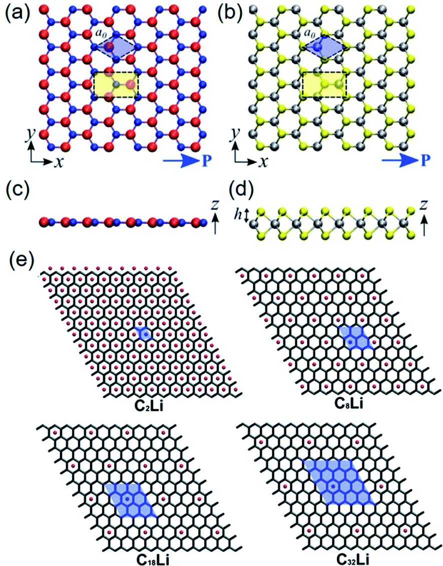 | ||
| Fig. 3 Top-view geometry of monolayer (a) h-BN and (b) trigonal prismatic molybdenum disulfide (2H–MoS2) (B atoms: red, N atoms: blue, Mo (transition metal) atoms: silver, S (chalcogenide) atoms: yellow). The axes and directions of piezoelectric polarization are designated. The hexagonal primitive cell is marked as blue regions. The orthorhombic unit cell applied in the density functional theory (DFT) simulations is marked as yellow regions. (c and d) Side-view geometry of the atomically thin h-BN monolayer and the 2H–MoS2 monolayer, respectively. (e) Modelling for different concentrations of Li components doped on graphene layers. Unit cell is marked as blue regions, and expressed by the formula unit CnLi in which n = 2, 8, 18, and 32. This figure has been adapted/reproduced from ref. 115 and 125 with permission from American Chemical Society, copyright 2012. | ||
2.2 Fabrication approaches and morphology modulation
A variety of fabrication approaches (e.g. hydrothermal method, sol–gel approach, solid–state reaction, electrospinning, molten salt reaction, mechanical exfoliating process, chemical exfoliating process, etc.) have been proposed for piezoelectric nanocrystals.54,121–124Table 2 lists some typical piezoelectric nanomaterials and corresponding fabrication approaches. The modulation of reaction parameters varies depending on typical fabrication approaches. Surely, the morphology of nanomaterials could be adjusted by reaction time, temperature, raw materials, pH value, and template types. The statements below explain the synthesis and fabrication methods for piezoelectric nanoparticles including 1D, 2D nanomaterials as well as 0D nanoparticles. We explain the representative fabrication methods in this section. It should be noted that some minor or scarce methods are skipped here such as laser ablation.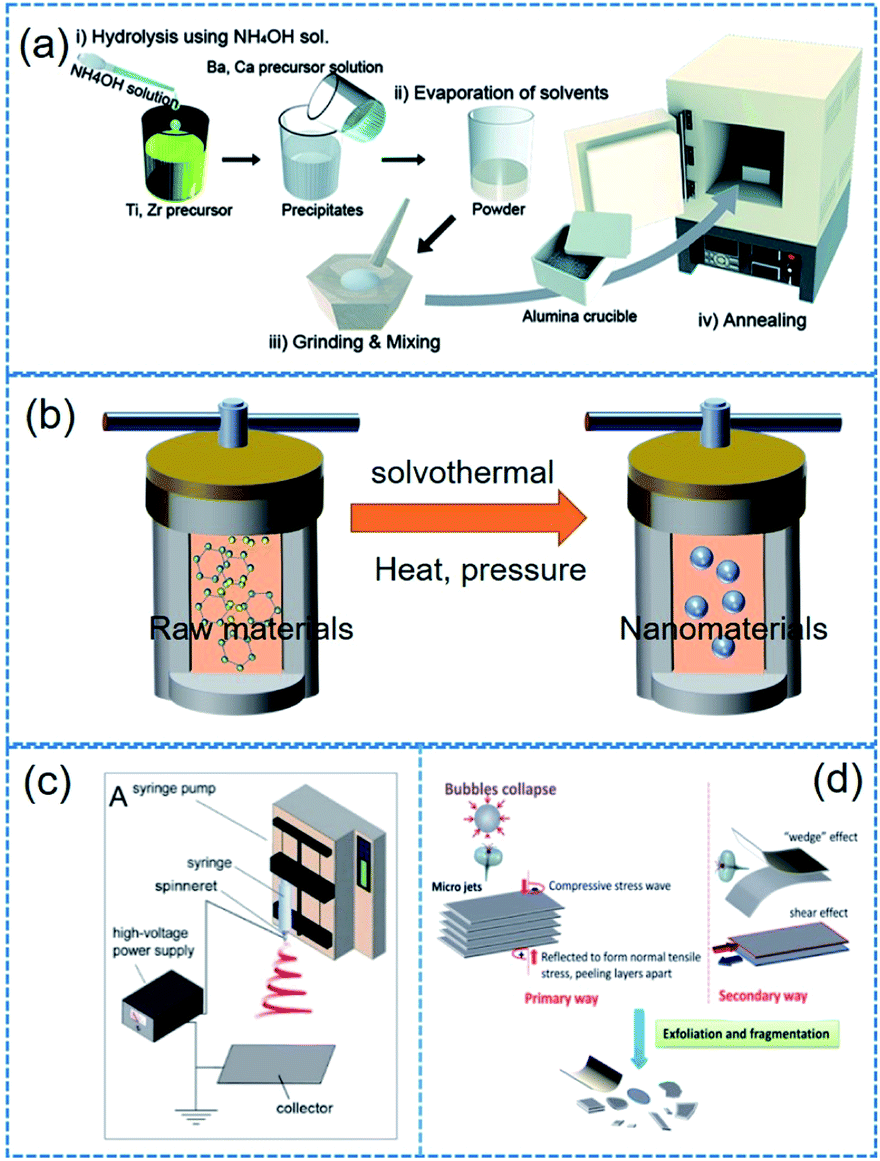 | ||
| Fig. 4 Illustrated flow chart of (a) sol–gel, (b) solvothermal/hydrothermal, (c) electrospinning, (d) mechanical exfoliating process. This figure has been adapted/reproduced from ref. 144, 156 and 159 with permission from American Chemical Society, copyright 2017; Royal Chemical Society, copyright 2015; and Royal Chemical Society, copyright 2016, respectively. | ||
(i) Electrospinning. Note that the electrospinning is not a synthesis method of nanoparticles. Electrospinning process is more suitable for long 1D microstructures or (sub-)nanostructures. However, we mentioned it here owing to its particular role in the application of piezoelectric nanoparticles. Electrospinning is a simple and versatile technique that relies on the electrostatic force between surface charges to continuously draw nanofibers from a viscoelastic fluid such as particle dispersions or sol–gel solutions.144 It has been adopted to successfully fabricate many piezoelectric nanofibers, including (Na1/2Bi1/2)TiO3–BaTiO3, BaTiO3, 0.5Ba(Zr0.2Ti0.8)O3–0.5(Ba0.7Ca0.3)TiO3, (Na1/2Bi1/2)TiO3, (K0.5Na0.5)NbO3, BiFeO3, ZnO, etc.71,145–149 The basic flow chart of electrospinning is presented in Fig. 4c. For only ceramic fibre structure, a high-temperature calcination and a crystallization must be needed. In contrast, the electrospinning provides composite fibres composed of polymer matrix and incorporated piezoelectric nanoparticles to form organic–inorganic hybrid piezoelectric fibers.150,151
(ii) Obtaining 2D materials. In 2004, Novoselov used adhesive tapes to exfoliate graphene from graphite, and then initiated the world-wide exploration on 2D materials.152 Mechanical exfoliating technology, which is characterized by simplicity and low cost, springs up due to the research fever on 2D materials.153 Although the adhesive tape-based mechanical exfoliation is the first leading technique for 2D materials, it is not suitable for making 2D material flake dispersions. Note that it is also highly different from 2D material film fabrications. Therefore, some modified mechanical exfoliation and chemical exfoliation processes were developed to obtain 2D material dispersions such as ball milling, sonication or intercalation (Fig. 4d).154–156 In Table 2, we show some examples of 2D materials which were obtained from mechanical or chemical exfoliating process.
3. Devices and applications
The increasing popularity of portable electronics and Internet of things (IoT) demands durable and self-maintaining energy sources, intriguing the extensive research on energy conversion devices such as thermoelectric, photovoltaic, piezoelectric devices, and so forth.23,155,176–183 According to other mechanical energy harvesting devices, piezoelectric devices relatively did not have critical drawbacks such as weak humidity resistance and related encapsulation difficulty as well as significant mechanical abrasion problem.23,184–186 Among them, piezoelectric energy harvesters, which directly convert mechanical energy input into electrical energy output, have been of an intense interest during the last decade for self-powered and ubiquitous applications.187–190 They are highly suitable for indoor and/or isolated environments such as bridge girders, bio-implantation, and broad sensor network systems.191–193 Note that the energy harvesters including nanomaterials are often called nanogenerators. Fig. 5 shows various piezoelectric nanogenerators (PNGs) that have been developed till now. Among the diverse piezoelectric nanogenerators, piezocomposite nanogenerators, which were firstly demonstrated by Park et al. in 2012,194 have highly attracted academic and industrial attentions because of their novel characteristics such as economy, scalability, efficient performance, and mechanically flexible properties.194–197 They consist of piezoelectric nanoscale filler and polymer matrix, often with additional mechanical agents.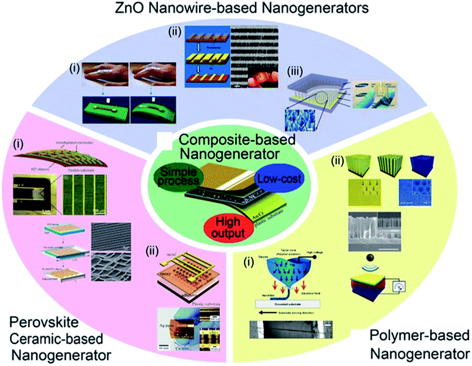 | ||
| Fig. 5 Diverse types of piezoelectric energy harvesters and nanogenerators. This figure has been adapted/reproduced from ref. 196 with permission from Springer, copyright 2016. | ||
Two kinds of polymer matrices have been mainly used for piezocomposite nanogenerators, i.e., non-piezoelectric polydimethylsiloxane (PDMS) polymer or poly(vinylidene fluoride) (PVDF)-based piezoelectric polymers. For advanced developments, some other polymer matrices have also been adopted such as Ecoflex silicone rubber,195 polyvinyl chloride (PVC),198 polycarbonate (PC),199 silk fibroin,200etc. For example, the intrinsic elongation rate of Ecoflex silicone rubber is up to ∼900%, which is a good choice for ultra-stretchable composite nanogenerators.195 Silk fibroin can be used as the matrix due to its natural biodegradability, which meets the requirement of biological and eco-friendly electronics.200 Besides polymer matrices, a myriad of inorganic piezoelectric fillers have been proposed, which serve as the active phases in piezoelectric nanogenerators.201,202
The last several years have witnessed the tremendous progress in lead-free piezoelectric nanoparticles, which endows the possibility for further designing high-performance piezoelectric composite energy harvesters. Enhanced energy storage devices (capacitors) are also another important research field of perovskite-structured nanomaterials and thin films.203–206 Nonetheless, we will only focus on the field of energy harvesting devices in this review because the energy storage devices are directly related to the dielectric and ferroelectric physics, rather than piezoelectric and electromechanical couplings.206–211 Hence, we will discuss piezoelectric energy harvesters based on lead-free piezoelectric nanoparticles and representative composite design strategies in this part.
3.1 Stress reinforcing and dispersing effects
As mentioned earlier, piezoelectric composite nanogenerators are generally fabricated by mixing piezoelectric nanoparticle fillers with a polymer matrix by physical stirring process. This process is characterized by low cost, easy controllability, mass-production compatibility, etc. For a long time, especially at the beginning period of piezoelectric nanogenerators, this approach has been considered to be the dominating and widely accepted method. However, there exist critical drawbacks, such as inhomogeneous filler distribution and ineffective stress transfer from external forces to internal piezoceramic components, which severely limit the energy harvesting performance from the active composite layers. To alleviate this problem, Park et al. proposed an efficient strategy, which is to introduce 1D conducting nanomaterials, e.g. copper nanorods, carbon nanotubes (CNTs), reduced graphene oxide, etc.194,212,213 It also contributes to reducing internal resistance and reactance for fast polarization switching.194Park et al. firstly investigated the positive effects of 1D conductive nanostructures on the mechanical energy harvesting capability of BaTiO3/PDMS nanocomposite generators. CNTs serve as physical dispersant, stress reinforcing agent, and conducting functional material, as shown clearly in Fig. 6a. The introduction of CNT results in a dramatically increasing energy harvesting output, as revealed in Fig. 6b. Jeong et al. also developed a more high-performance lead-free nanocomposite generator by including metal nanorod fillers (i.e. copper nanorod) and high-quality lead-free 0.942(K0.480Na0.535)NbO3–0.058LiNbO3 nanoparticles into PDMS matrix.212Fig. 6c–e shows the overall device configuration and the real device pictures of the flexible high-output lead-free piezoelectric composite generator. Similar with CNTs, the metal nanorods also acted as an excellent dispersant and a secondary filler in the composite energy harvester, as presented by the scanning electron microscopy (SEM) images (Fig. 6f and g). Note that the stress reinforcement and the dispersion effects are attributed to the 1D geometrical factor of nanotubes, nanorods, and nanowires by effective percolation and entanglement as well as higher Young's modulus within the matrix. Therefore, the 1D piezoelectric (insulating) nanomaterials can also induce self-mechanical improvement. Although the conductive property is not directly affect the mechanical enhancement, it can additionally bestow the ability to present electrical benefits of piezoelectric composites. For example, the conductive filler could reduce the internal resistance of piezoelectric nanocomposite, resulting in the decrement of matching impedance in a final circuit, which is advantageous to device operation. The conductive factor and low internal resistance also shortens a time constant in a RC discharging process, causing the increment of output voltage.194 This RC discharging process is also important for poling process of the piezoelectric nanogenerator devices. Recently, AC poling process can be more effective than DC poling process in some cases to achieve not only high piezoelectric performance but also domain direction-related transparency.214 This effect may be associated with the RC conductivity in the piezoelectric nanocomposite.
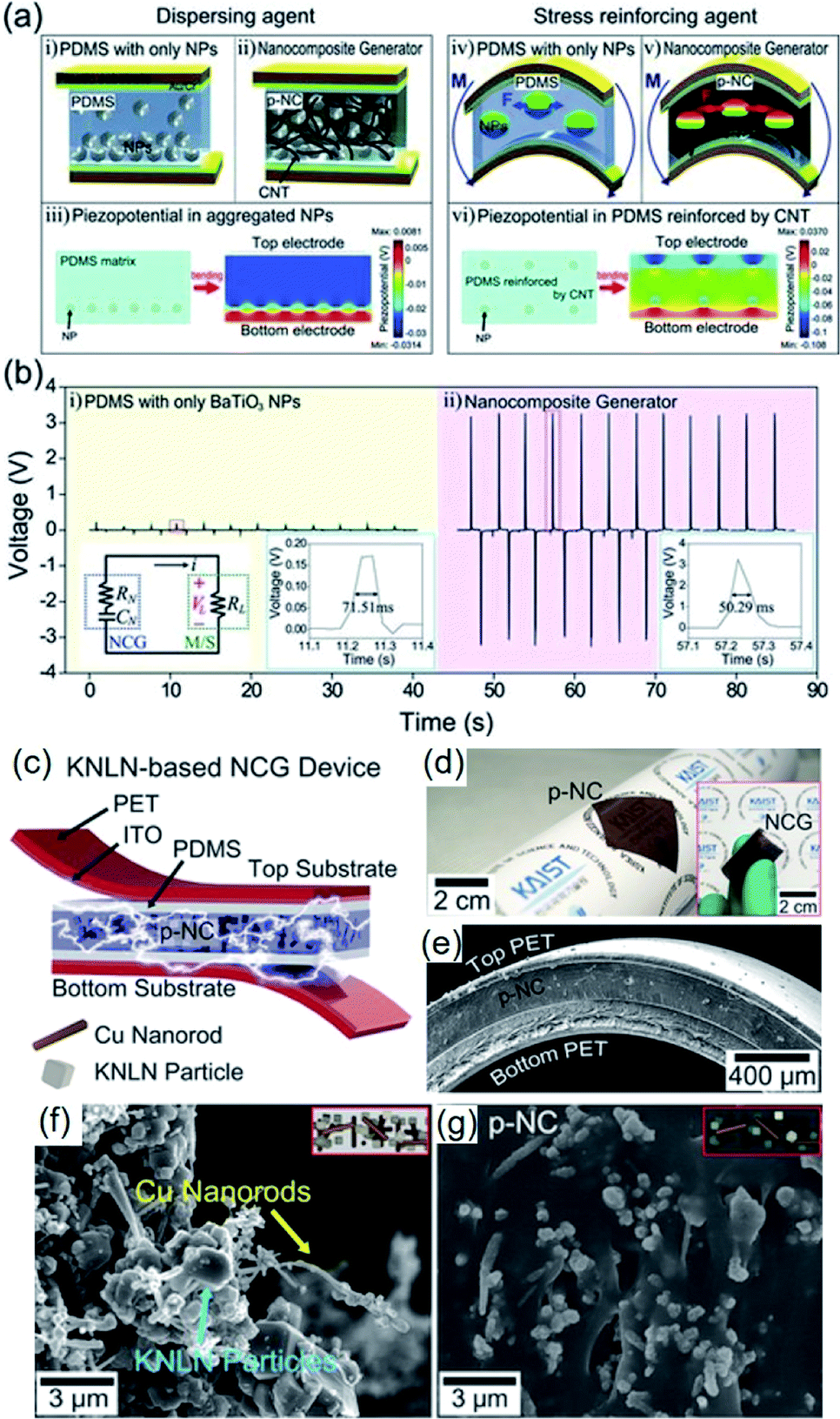 | ||
| Fig. 6 (a) Schematic illustrations of the cross-sectional architecture of nanocomposite generator (abbreviated as NCG) and the simulated piezoelectric potential distributions. The CNTs serve as dispersants (ii) and mechanical reinforcing agents (v) that are well described by the calculated piezoelectric simulations (iii and vi). (b) Voltages generated from the composite devices consisting of only BaTiO3 NPs and the NCG structure. The right insets present high resolution of output voltage signals. The left inset is the circuit diagram of the measurement system. (c) Schematic illustration of an NCG structure using high-quality lead-free 0.942(K0.480Na0.535)NbO3–0.058LiNbO3 nanoparticles and Cu nanorod fillers with PDMS matrix. (d) Camera photograph of the flexible piezoelectric nanocomposite (p-NC) layer. The inset presents the final NCG device with electrodes/plastic substrates, bent by fingers. (e) Cross-sectional SEM image of the NCG device. (f) Magnified SEM image of the mixed nanomaterials consisting of 0.942(K0.480Na0.535)NbO3–0.058LiNbO3 nanoparticles and Cu nanorod before PDMS mixing. (g) SEM image of the cross-sectional p-NC layer with PDMS matrix. This figure has been adapted/reproduced from ref. 194 and 212 with permission from John Wiley & Sons, copyright 2012 and 2014, respectively. | ||
3.2 Construction of fibre composite structures
Fabrication of core–shell fibre structures is another efficient strategy for high-performance composite nanogenerators for flexible device applications.70,215–217Fig. 7 shows the typical examples of this configuration. For these kinds of composite devices, the fabrication procedure could be divided into three steps: (i) mixing piezoelectric nanoparticles and polymer matrix in solvent or dispersant, (ii) spinning methods (mainly electrospinning), (iii) coating electrodes and/or attaching substrate (Fig. 7a). This kind of configuration combines the high flexibility of fibre-structured polymer matrix and the good piezoresponse of embedded piezoelectric nanoparticles. When the matrix is piezoelectric polymer such as PVDF-based copolymers, the piezoelectric nanoparticles affect the dipole of polymeric chain structures sometimes (Fig. 7b).216 Due to its intrinsic fibre structure, it is suitable for being integrated with textiles for wearable electronics, as well demonstrated in the previous studies.218 Therefore, the use of lead-free piezoelectric nanoparticles is very crucial for biocompatible characteristics of wearable and biomedical device applications. In addition, the integration of electrode materials into each fibre without substrates is still challenging even though it is highly important to achieve real piezoelectric clothes for self-powered wearable electronics. The dielectric properties of polymer matrix in the fibre structure can also affect the device performance. In particular, the electrical breakdown may be one of the representative problems due to the emerging electrical path along with the fibre geometry. We can expect that new approaches to overcome the limitations of polymeric dielectric strength through magnetic or optical processes.219,220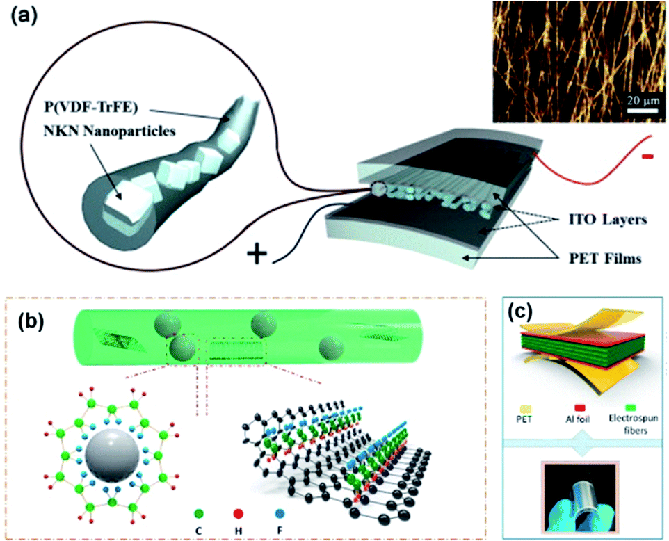 | ||
| Fig. 7 (a) Schematics of a (Na,K)NbO3 (NKN)/poly(vinlyidene fluoride–trifluoroethylene) (P(VDF–TrFE)) composite nanofiber-based nanogenerator device (inset: optical microscope image of the piezocomposite nanofibers). (b and c) The mechanism diagram for the formation of β phase of PVDF-based polymer on BT nanoparticles and graphene nanosheets in the nanocomposite fibre and the final device structure with electrodes. This figure has been adapted/reproduced from ref. 70 and 216 with permission from Elsevier, copyright 2015 and 2018, respectively. | ||
3.3 Modified distribution of nanoparticles in polymer matrix
In addition to the aforementioned strategies, some special structure designs have been proposed, as exemplarily shown in Fig. 8. The hemispherical BaTiO3–poly(vinylidene fluoride-co-hexafluoropropylene) (P(VDF–HFP)) clusters were realized by a simple solvent evaporation method, as illustrated in Fig. 8a–c.221 After attaching top and bottom electrodes with PDMS buffer layers (Fig. 8d and e), a sandwich-type flexible piezoelectric composite nanogenerator was obtained (Fig. 8f). Using the evaporation of solvent, BaTiO3 nanoparticles aggregate together to form hemisphere structures on the composite surface (Fig. 8g). In this research, P(VDF–HFP) served as the tight linker to make aggregated BaTiO3 clusters possible. The increasing mechanical energy harvesting performance could actually be ascribed to the effective piezopotential distribution by the hemispherical structures, as also proved by COMSOL Multiphysics simulations.221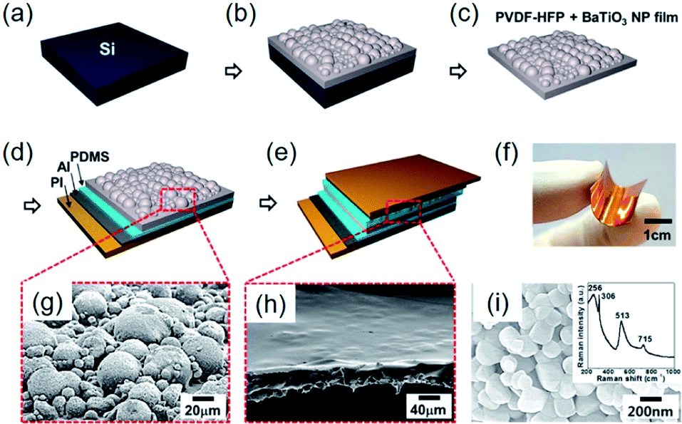 | ||
| Fig. 8 (a–e) Schematic fabrication steps of the hemispherical-structured composite nanogenerator fabrication process. (a) Si wafer as a substrate. (b) BaTiO3–P(VDFP–HFP) composite film cured through solvent evaporation after spin coating on the substrate. (c) Peeled off the nanocomposite film from the Si wafer substrate. (d) PDMS-coated Al electrode is attached on the bottom side. (e) PDMS spin coating on BaTiO3–P(VDF–HFP) nanocomposite film, followed by the formation of the top electrode. (f) Photograph of the final form of fabricated nanogenerator, showing the mechanical flexibility. (g) SEM image of the BaTiO3–P(VDF–HFP) nanocomposite composed of BaTiO3–P(VDF–HFP) hemispherical clusters. (h) SEM image of the PDMS-covered BaTiO3–P(VDF–HFP) composite layer. (i) SEM image of the BaTiO3 nanoparticles used in that research. Inset: a Raman spectrum obtained from the BaTiO3 nanoparticles. This figure has been adapted/reproduced from ref. 221 with permission from American Chemical Society, copyright 2014. | ||
Recently, Zhang et al. came up with a novel idea to design a fully three-dimensional (3D) interconnected inorganic filler network with a polymer matrix to dramatically increase the stress transfer ability and demonstrated its beneficial effect on improving piezoelectric energy harvesting capability.32,33,179 The structure is presented in Fig. 9. With mimicking the comprehensive properties of sea sponges (e.g. mechanical flexibility, recoverability, interconnected network structure, etc.), 3D piezoelectric ceramic skeleton was fabricated by combining the lead-free piezoelectric sol–gel processed (Ba,Ca)(Zr,Ti)O3 (BCZT) and the suitable calcination/crystallization. The 3D interconnected porous framework structure (the left of Fig. 9a) is based on the natural sea sponge (the inset of Fig. 9a). On the other hand, the right of Fig. 9a is the structure of the conventional polymer composite containing randomly dispersed particles. Regardless of the particle size of piezoelectric ceramic fillers in the polymer matrix, the conventional polymer–ceramic composite has almost the same configuration with the right of Fig. 9a. It should be mentioned at least briefly that the drawback of this kind of structure lies on the problems as follows: (i) the aggregation of fillers due to the randomly dispersed nanoparticles and (ii) the deteriorated stress-transfer ability because the low elastic modulus of polymer matrix. The phase-field simulations clearly demonstrated that the stress distribution in the 3D interconnected structure is much more uniform than that in composites containing randomly distributed particles- under the same applied strain, as shown in Fig. 9b. Moreover, the average stress in the 3D interconnected composite is about 4 times higher than that in the random-particle-based polymer composite. The reinforced mechanical response of the bioinspired structure is apparently due to the fact that the interconnected BCZT 3D structure is capable of efficiently transferring stress from outside to the ceramic fillers, whereas the random-particle-based composite relaxes and dissipates most of the stress within the soft polymer matrix rather than transferring it to the BCZT ceramic particles. The generated piezoelectric potential of 3D interconnected composite is, indeed, greater than that of random-particle-based composite, as presented in Fig. 9c. As expected, the energy harvesting ability of the 3D interconnected composite is superior to the random-particle-based composite. This research guided researchers to a new approach to the application of lead-free piezoelectric nanomaterials. This composite design is also available directly using nanoparticle dispersions without sol–gel solutions using accompanied fibril dispersion.32
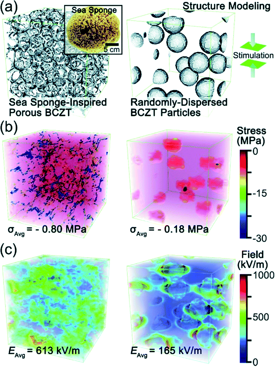 | ||
| Fig. 9 (a) Structural modelling of a sea sponge-inspired BCZT composite and a randomly dispersed BCZT particle-based composite by using the phase-field simulation with the Fourier spectral iterative perturbation method. (b) Computation results of the formed stress within the composites when a compressive strain of 12% is applied. (c) Computation results of the piezopotential-based electrical field generated within the composites when 12% strain is applied. This figure has been adapted/reproduced from ref. 33 with permission from Royal Chemical Society, copyright 2018. | ||
3.4 Incorporation of 2D piezoelectric nanofiller materials in polymer matrix
2D materials in the view of piezoelectricity have been considered a unique category for specific piezoelectric device and applications.222,223 Recently, the device configuration for composite nanogenerators has intrigued researchers' attentions.224Fig. 10a shows the method for obtaining h-BN nanoflakes using mechanochemcial exfoliation. First, the h-BN nanoflakes were directly transferred to line-patterned electrodes to evaluate the piezoelectric energy harvesting property of single h-BN nanoflake, as presented in Fig. 10b.155 The piezoelectric voltage coefficient of a single BN nanoflake and the mechanical energy harvesting performance of BN based nanongenerator were quantified. Finally, the 2D piezoelectric h-BN nanoflakes were embedded into the PDMS elastomer matrix to fabricate a nanocomposite generator showing the energy harvesting performance of ∼9 V and ∼200 nA (Fig. 10c and d). In this configuration, the 2D nanoflakes act as the piezoelectric nanoparticles and nanofillers in the conventional nanocomposite generators. Nevertheless, the 2D piezoelectric material-based composite should be more investigated, because the ferroelectric properties of 2D materials are still veiled in spite of their piezoelectric characteristics. Hence, it is dim whether the external poling is possible or not for randomly distributed 2D nanomaterials. If the 2D material is only piezoelectric but not ferroelectric, the piezoelectric dipole within the piezocomposite must also be random and cannot be aligned in a unified direction (like the composite of ZnO particles), which means the composite configuration of piezoelectric 2D materials is not reliable in contrast to the previously reported plane configuration of 2D sheets.225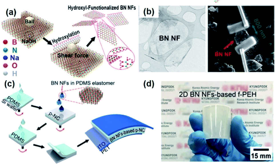 | ||
| Fig. 10 (a) Schematic illustration of the sequential process for fabricating 2D h-BN nanoflakes. (b) Transmission electron microscopy (TEM) image of a h-BN nanoflake and the SEM image of a h-BN single nanoflake connected to two Au line electrodes formed by the focused ion beam (FIB)-assisted deposition method. (c) Illustration of the device fabrication of piezoelectric h-BN nanoflakes-based elastomeric nanocomposite generator and (d) its real photograph presenting flexible configuration. This figure has been adapted/reproduced from ref. 155 with permission from American Chemical Society, copyright 2019. | ||
3.5 Applications by energy harvesting signals
As stated above, we summarized several typical strategies that researchers proposed to improve the performance of piezoelectric nanogenerators using lead-free perovskite nanoparticles. The high-output performance as well as the facile fabrication process make the nanogenerators qualified in some intriguing fields such as soft-robotics, wearable sensing systems, cell stimulation and so forth.4. Summary and outlook
Piezoelectric nanomaterials, in particular environmentally friendly lead-free piezoelectrics, have been an important class of materials both for fundamental research and applications for the past 20 years. It is predicted that piezoelectric properties at nanometer scales would be dramatically different from those of bulk materials or polycrystalline films. Fortunately, the complex interplay between multiple degrees of unprecedented output performances of these nanomaterials demonstrates that techniques developed to investigate them have been applied to other research fields with a great success. Each year brings new insights and new understanding of these complex materials as a new potential for energy harvesting applications. Specifically, as an important type of energy devices, piezo-nanocomposite-based energy harvesters have attracted great attention by the research community due to a broad spectrum of their unique applications such as self-powered portable sensors, transportation, energy distribution, smart home, military weapons, and biomedical devices, and so on.It clearly indicates that this complex class of materials will continue to attract interest as their performance in the existing devices is improved and novel applications are developed in the years to come. In this review, we provided a synopsis of the major developments and achievements in the current and past years in the area of lead-free piezoelectric nanomaterials and related energy harvesting devices with a strong emphasis on work blazing a new trail in terms of methods and control of material properties at scales, understanding of size effects, and routes to develop new functionalities and improved performance in piezoelectric nanomaterials-based energy harvesting devices.
This review began with a short introduction and a brief discussion of several representative lead-free piezoelectric nanoparticles with various chemical compositions and different crystal structures, followed by the detailed discussion on the state-of-the-art for lead-free piezoelectric nanoparticles with diverse morphological configurations and chemical features, and synthesis methodologies such as solid-state reactions, sol–gel methods, hydrothermal or solvothermal syntheses, molten salt reactions, supercritical fluid technologies, and so on. Then we commented on the applications of lead-free piezoelectric nanoparticles, especially in piezoelectric nanocomposite-based energy harvesting device applications. Finally, we completed this review with a short summary and future outlook of lead-free piezoelectric nanomaterials and devices.
Despite the progress accomplished through those approaches, several issues still remain to be addressed for further improvement. We would like to wrap-up this review with brief comments for a better perspective of this field as follows.
(i) Further clarification of the underlying physics of piezoelectric mechanism at nanoscale.
(ii) Finding new scalable and mass-producible fabrication methods.
(iii) Development of a novel characterization tool or method to evaluate the properties of piezoelectric nanostructures.
(iv) A better understanding of degradation and failure of lead-free piezoelectric nanomaterials and devices using macro- and microscopic measurements and accurate simulation and modelling.
(v) Innovative device designs based on the optimal input parameters of lead-free piezoelectric nanomaterials; thus, guiding and supporting the understanding of performance by comparison of experiment and simulation.
Conflicts of interest
There are no conflicts to declare.Acknowledgements
This research was supported by Basic Science Research Program through the National Research Foundation of Korea (NRF) funded by the Ministry of Science and ICT (NRF-2019R1C1C1002571). This work was also supported by the Start-up Funding of Wuhan University of Technology (Grant No. 40120490). Authors at Brown University would like to thank for the support from National Science Foundation (NSF) under Award No. 1408344.Notes and references
- Y. Zhang, H. Sun and W. Chen, J. Phys. Chem. Solids, 2018, 114, 207–219 CrossRef CAS.
- Y. Liu, H. Aziguli, B. Zhang, W. Xu, W. Lu, J. Bernholc and Q. Wang, Nature, 2018, 562, 96–100 CrossRef CAS PubMed.
- J. Rödel, W. Jo, K. T. P. Seifert, E.-M. Anton, T. Granzow and D. Damjanovic, J. Am. Ceram. Soc., 2009, 92, 1153–1177 CrossRef.
- K. Gupta, S. Brahma, J. Dutta, B. Rao and C.-P. Liu, Nano Energy, 2019, 55, 1–21 CrossRef CAS.
- T. Zheng, J. Wu, D. Xiao and J. Zhu, Prog. Mater. Sci., 2018, 98, 552–624 CrossRef CAS.
- S. Zhang, F. Li, F. Yu, X. Jiang, H.-Y. Lee, J. Luo and T. R. Shrout, J. Korean Ceram. Soc., 2018, 55, 419–439 CrossRef CAS.
- E. Cross, Nature, 2004, 432, 24–25 CrossRef CAS PubMed.
- J. Rödel, K. G. Webber, R. Dittmer, W. Jo, M. Kimura and D. Damjanovic, J. Eur. Ceram. Soc., 2015, 35, 1659–1681 CrossRef.
- C. K. Jeong, J. H. Han, H. Palneedi, H. Park, G.-T. Hwang, B. Joung, S.-G. Kim, H. J. Shin, I.-S. Kang, J. Ryu and K. J. Lee, APL Mater., 2017, 5, 074102 CrossRef.
- H.-P. Kim, C. W. Ahn, Y. Hwang, H.-Y. Lee and W. Jo, J. Korean Ceram. Soc., 2017, 54, 86–95 CrossRef CAS.
- C.-H. Hong, H.-P. Kim, B.-Y. Choi, H.-S. Han, J. S. Son, C. W. Ahn and W. Jo, J. Materiomics, 2016, 2, 1–24 CrossRef.
- T. R. Shrout and S. J. Zhang, J. Electroceramics, 2007, 19, 111–124 CAS.
- Y. Zhang, H.-J. Sun and W. Chen, J. Alloys Compd., 2017, 694, 745–751 CrossRef CAS.
- Y. Saito, H. Takao, T. Tani, T. Nonoyama, K. Takatori, T. Homma, T. Nagaya and M. Nakamura, Nature, 2004, 432, 84–87 CrossRef CAS PubMed.
- H. Sun, Y. Zhang, X. Liu, Y. Liu and W. Chen, Ceram. Int., 2015, 41, 555–565 CrossRef CAS.
- X.-Q. Fang, J.-X. Liu and V. Gupta, Nanoscale, 2013, 5, 1716 RSC.
- C. Falconi, Nano Energy, 2019, 59, 730–744 CrossRef CAS.
- L. Q. Cheng and J. F. Li, J. Materiomics, 2016, 2, 25–36 CrossRef.
- J. Zhang, C. Wang and C. Bowen, Nanoscale, 2014, 6, 13314–13327 RSC.
- B. Jiang, J. Iocozzia, L. Zhao, H. Zhang, Y.-W. Harn, Y. Chen and Z. Lin, Chem. Soc. Rev., 2019, 48, 1194–1228 RSC.
- R. Ding, H. Liu, X. Zhang, J. Xiao, R. Kishor, H. Sun, B. Zhu, G. Chen, F. Gao, X. Feng, J. Chen, X. Chen, X. Sun and Y. Zheng, Adv. Funct. Mater., 2016, 26, 7708–7716 CrossRef CAS.
- Z. L. Wang and J. Song, Science, 2006, 312, 242–246 CrossRef CAS PubMed.
- B.-Y. Lee, D. H. Kim, J. Park, K.-I. Park, K. J. Lee and C. K. Jeong, Sci. Technol. Adv. Mater., 2019, 20, 758–773 CrossRef PubMed.
- A. Ahmed, I. Hassan, M. F. El-Kady, A. Radhi, C. K. Jeong, P. R. Selvaganapathy, J. Zu, S. Ren, Q. Wang and R. B. Kaner, Adv. Sci., 2019, 1802230 CrossRef CAS PubMed.
- G. T. Hwang, M. Byun, C. K. Jeong and K. J. Lee, Adv. Healthc. Mater., 2015, 4, 646–658 CrossRef CAS PubMed.
- H. S. Lee, J. Chung, G.-T. Hwang, C. K. Jeong, Y. Jung, J.-H. Kwak, H. Kang, M. Byun, W. D. Kim, S. Hur, S.-H. Oh and K. J. Lee, Adv. Funct. Mater., 2014, 24, 6914–6921 CrossRef CAS.
- C. K. Jeong, D. Y. Hyeon, G.-T. Hwang, G.-J. Lee, M.-K. Lee, J.-J. Park and K.-I. Park, J. Mater. Chem. A, 2019, 7, 25481–25489 RSC.
- S. S. Won, H. Seo, M. Kawahara, S. Glinsek, J. Lee, Y. Kim, C. K. Jeong, A. I. Kingon and S.-H. Kim, Nano Energy, 2019, 55, 182–192 CrossRef CAS.
- H. Yuan, T. Lei, Y. Qin and R. Yang, Nano Energy, 2019, 59, 84–90 CrossRef CAS.
- L. Jin, B. Zhang, L. Zhang and W. Yang, Nano Energy, 2019, 66, 104086 CrossRef CAS.
- C. Dagdeviren, B. D. Yang, Y. Su, P. L. Tran, P. Joe, E. Anderson, J. Xia, V. Doraiswamy, B. Dehdashti, X. Feng, B. Lu, R. Poston, Z. Khalpey, R. Ghaffari, Y. Huang, M. J. Slepian and J. A. Rogers, Proc. Natl. Acad. Sci., 2014, 111, 1927–1932 CrossRef CAS PubMed.
- Y. Zhang, C. K. Jeong, J. Wang, H. Sun, F. Li, G. Zhang, L.-Q. Chen, S. Zhang, W. Chen and Q. Wang, Nano Energy, 2018, 50, 35–42 CrossRef CAS.
- Y. Zhang, C. K. Jeong, T. Yang, H. Sun, L.-Q. Chen, S. Zhang, W. Chen and Q. Wang, J. Mater. Chem. A, 2018, 6, 14546–14552 RSC.
- J. K. Han, S. Kim, S. Jang, Y. R. Lim, S.-W. Kim, H. Chang, W. Song, S. S. Lee, J. Lim, K.-S. An and S. Myung, Nano Energy, 2019, 61, 471–477 CrossRef CAS.
- H. Wei, H. Wang, Y. Xia, D. Cui, Y. Shi, M. Dong, C. Liu, T. Ding, J. Zhang, Y. Ma, N. Wang, Z. Wang, Y. Sun, R. Wei and Z. Guo, J. Mater. Chem. C, 2018, 6, 12446–12467 RSC.
- R. Ding, X. Zhang, G. Chen, H. Wang, R. Kishor, J. Xiao, F. Gao, K. Zeng, X. Chen, X. W. Sun and Y. Zheng, Nano Energy, 2017, 37, 126–135 CrossRef CAS.
- D. Mohanty, G. S. Chaubey, A. Yourdkhani, S. Adireddy, G. Caruntu and J. B. Wiley, RSC Adv., 2012, 2, 1913 RSC.
- M. Minary-Jolandan, R. A. Bernal, I. Kuljanishvili, V. Parpoil and H. D. Espinosa, Nano Lett., 2012, 12, 970–976 CrossRef CAS PubMed.
- H. Y. S. Al-Zahrani, J. Pal and M. A. Migliorato, Nano Energy, 2013, 2, 1214–1217 CrossRef CAS.
- K. H. Michel and B. Verberck, Phys. Rev. B: Condens. Matter Mater. Phys., 2009, 80, 224301 CrossRef.
- J. Seo, Y. Kim, W. Y. Park, J. Y. Son, C. K. Jeong, H. Kim and W. H. Kim, Appl. Surf. Sci., 2019, 487, 1356–1361 CrossRef CAS.
- Y. Liu, H.-L. Cai, M. Zelisko, Y. Wang, J. Sun, F. Yan, F. Ma, P. Wang, Q. N. Chen, H. Zheng, X. Meng, P. Sharma, Y. Zhang and J. Li, Proc. Natl. Acad. Sci., 2014, 111, E2780–E2786 CrossRef CAS PubMed.
- S. K. Karan, S. Maiti, O. Kwon, S. Paria, A. Maitra, S. K. Si, Y. Kim, J. K. Kim and B. B. Khatua, Nano Energy, 2018, 49, 655–666 CrossRef CAS.
- X. Song, F. Hui, T. Knobloch, B. Wang, Z. Fan, T. Grasser, X. Jing, Y. Shi and M. Lanza, Appl. Phys. Lett., 2017, 111, 083107 CrossRef.
- J. Qi, Y.-W. Lan, A. Z. Stieg, J.-H. Chen, Y.-L. Zhong, L.-J. Li, C.-D. Chen, Y. Zhang and K. L. Wang, Nat. Commun., 2015, 6, 7430 CrossRef CAS PubMed.
- R. M. F. Baptista, E. de Matos Gomes, M. M. M. Raposo, S. P. G. Costa, P. E. Lopes, B. Almeida and M. S. Belsley, Nanoscale Adv, 2019, 1, 4339–4346 RSC.
- S. Chandratre and P. Sharma, Appl. Phys. Lett., 2012, 100, 023114 CrossRef.
- I. Chae, C. K. Jeong, Z. Ounaies and S. H. Kim, ACS Appl. Bio Mater., 2018, 1, 936–953 CrossRef CAS.
- T. Takenaka, H. Nagata and Y. Hiruma, Jpn. J. Appl. Phys., 2008, 47, 3787–3801 CrossRef CAS.
- S. Zhang, R. Xia and T. R. Shrout, J. Electroceramics, 2007, 19, 251–257 CrossRef CAS.
- T. H. Im, D. Y. Park, H. K. Lee, J. H. Park, C. K. Jeong, D. J. Joe and K. J. Lee, Part. Part. Syst. Charact., 2017, 34, 1600429 CrossRef.
- L. Liu, F. Gao, Y. Zhang and H. Sun, J. Alloys Compd., 2014, 616, 293–299 CrossRef CAS.
- F. R. Fan, W. Tang and Z. L. Wang, Adv. Mater., 2016, 28, 4283–4305 CrossRef CAS PubMed.
- P. M. Rørvik, T. Grande and M. A. Einarsrud, Adv. Mater., 2011, 23, 4007–4034 CrossRef PubMed.
- Y. Li, Y. Zhang, H. Sun, X. Liu, H. Sui, D. Zhou and Q. Guo, J. Mater. Sci. Mater. Electron., 2018, 29, 7851–7856 CrossRef CAS.
- J. Wu, H. Shi, T. Zhao, Y. Yu and S. Dong, Adv. Funct. Mater., 2016, 26, 7186–7194 CrossRef CAS.
- D. Wang, Z. Fan, W. Li, D. Zhou, A. Feteira, G. Wang, S. Murakami, S. Sun, Q. Zhao, X. Tan and I. M. Reaney, ACS Appl. Energy Mater., 2018, 1, 4403–4412 CrossRef CAS.
- Y.-J. Dai, S. Zhang, T. R. Shrout and X.-W. Zhang, J. Am. Ceram. Soc., 2010, 93, 1108–1113 CrossRef CAS.
- Y. Zhang, H. Sun and W. Chen, Ceram. Int., 2015, 41, 8520–8532 CrossRef CAS.
- H. Guo, Y. Li, Y. Zhang, H. Sun and X. Liu, J. Mater. Sci. Mater. Electron., 2018, 29, 19063–19069 CrossRef CAS.
- B. Jaffe, R. S. Roth and S. Marzullo, J. Appl. Phys., 1954, 25, 809–810 CrossRef CAS.
- B. Xiong, H. Hao, S. Zhang, H. Liu and M. Cao, J. Am. Ceram. Soc., 2011, 94, 3412–3417 CrossRef CAS.
- H. Wu, Y. Zhang, J. Wu, J. Wang and S. J. Pennycook, Adv. Funct. Mater., 2019, 29, 1902911 CrossRef.
- M. H. Lee, D. J. Kim, J. S. Park, S. W. Kim, T. K. Song, M.-H. Kim, W.-J. Kim, D. Do and I.-K. Jeong, Adv. Mater., 2015, 27, 6976–6982 CrossRef CAS PubMed.
- L. Q. Cheng, K. Wang, Q. Yu and J. F. Li, J. Mater. Chem. C, 2014, 2, 1519–1524 RSC.
- P. K. Panda, J. Mater. Sci., 2009, 44, 5049–5062 CrossRef CAS.
- S. S. Won, J. Lee, V. Venugopal, D.-J. Kim, J. Lee, I. W. Kim, A. I. Kingon and S.-H. Kim, Appl. Phys. Lett., 2016, 108, 232908 CrossRef.
- J. Kwak, A. I. Kingon and S.-H. Kim, Mater. Lett., 2012, 82, 130–132 CrossRef CAS.
- J. Wu, D. Xiao and J. Zhu, Chem. Rev., 2015, 115, 2559–2595 CrossRef CAS PubMed.
- H. B. Kang, C. S. Han, J. C. Pyun, W. H. Ryu, C.-Y. Kang and Y. S. Cho, Compos. Sci. Technol., 2015, 111, 1–8 CrossRef CAS.
- Y. M. Yousry, K. Yao, X. Tan, A. M. Mohamed, Y. Wang, S. Chen and S. Ramakrishna, ACS Appl. Mater. Interfaces, 2019, 11, 23503–23511 CrossRef CAS PubMed.
- H. J. Seog, A. Ullah, C. W. Ahn, I. W. Kim, S. Y. Lee, J. Park, H. J. Lee, S. S. Won and S.-H. Kim, J. Korean Phys. Soc., 2018, 72, 1467–1483 CrossRef.
- C. Sun, X. Xing, J. Chen, J. Deng, L. Li, R. Yu, L. Qiao and G. Liu, Eur. J. Inorg. Chem., 2007, 2007, 1884–1888 CrossRef.
- Y. Li, Z. Liao, F. Fang, X. Wang, L. Li and J. Zhu, Appl. Phys. Lett., 2014, 105, 182901 CrossRef.
- M. Acosta, N. Novak, V. Rojas, S. Patel, R. Vaish, J. Koruza, G. A. Rossetti and J. Rödel, Appl. Phys. Rev., 2017, 4, 041305 Search PubMed.
- W. Liu and X. Ren, Phys. Rev. Lett., 2009, 103, 257602 CrossRef PubMed.
- Z. Zhao, V. Buscaglia, M. Viviani, M. T. Buscaglia, L. Mitoseriu, A. Testino, M. Nygren, M. Johnsson and P. Nanni, Phys. Rev. B: Condens. Matter Mater. Phys., 2004, 70, 024107 CrossRef.
- C. Baek, J. E. Wang, S. Ryu, J.-H. Kim, C. K. Jeong, K.-I. Park and D. K. Kim, RSC Adv., 2017, 7, 2851–2856 RSC.
- G. Philippot, C. Elissalde, M. Maglione and C. Aymonier, Adv. Powder Technol., 2014, 25, 1415–1429 CrossRef CAS.
- D. Caruntu, T. Rostamzadeh, T. Costanzo, S. Salemizadeh Parizi and G. Caruntu, Nanoscale, 2015, 7, 12955–12969 RSC.
- P. Xue, H. Wu, W. Xia, Z. Pei, Y. Lu and X. Zhu, J. Am. Ceram. Soc., 2019, 102, 2325–2336 CrossRef CAS.
- Z.-H. Lin, Y. Yang, J. M. Wu, Y. Liu, F. Zhang and Z. L. Wang, J. Phys. Chem. Lett., 2012, 3, 3599–3604 CrossRef CAS PubMed.
- B. Moorthy, C. Baek, J. E. Wang, C. K. Jeong, S. Moon, K.-I. Park and D. K. Kim, RSC Adv., 2017, 7, 260–265 RSC.
- A. Koka and H. A. Sodano, Nat. Commun., 2013, 4, 2682 CrossRef PubMed.
- Z. Zhou, H. Tang and H. A. Sodano, Adv. Mater., 2014, 26, 7547–7554 CrossRef CAS PubMed.
- A. Nafari, C. C. Bowland and H. A. Sodano, Nano Energy, 2017, 31, 168–173 CrossRef CAS.
- C. K. Jeong, C. Baek, A. I. Kingon, K.-I. Park and S.-H. Kim, Small, 2018, 14, 1704022 CrossRef PubMed.
- B. N. Rao, A. N. Fitch and R. Ranjan, Phys. Rev. B: Condens. Matter Mater. Phys., 2013, 87, 060102 CrossRef.
- Y. Li, W. Chen, J. Zhou, Q. Xu, H. Sun and R. Xu, Mater. Sci. Eng., B, 2004, 112, 5–9 CrossRef.
- G. Wang, Y. Li, C. A. Murray, C. C. Tang and D. A. Hall, J. Am. Ceram. Soc., 2017, 100, 3293–3304 CrossRef CAS.
- C.-H. Hong, Z. Fan, X. Tan, W.-S. Kang, C. W. Ahn, Y. Shin and W. Jo, J. Eur. Ceram. Soc., 2018, 38, 5375–5381 CrossRef CAS.
- A. R. Paterson, H. Nagata, X. Tan, J. E. Daniels, M. Hinterstein, R. Ranjan, P. B. Groszewicz, W. Jo and J. L. Jones, MRS Bull., 2018, 43, 600–606 CrossRef CAS.
- H.-P. Kim, G.-J. Lee, H. Y. Jeong, J.-H. Jang, G.-Y. Kim, S.-Y. Choi, H.-Y. Lee, S.-G. Lee and W. Jo, J. Eur. Ceram. Soc., 2019, 39, 3327–3331 CrossRef CAS.
- C.-H. Hong, H. Guo, X. Tan, J. E. Daniels and W. Jo, J. Materiomics, 2019, 5, 634–640 CrossRef.
- X. Yang, R. Zeng, Z. Ren, Y. Wu, X. Chen, M. Li, J. Chen, R. Zhao, D. Zhou, Z. Liao, H. Tian, Y. Lu, X. Li, J. Li and G. Han, ACS Appl. Mater. Interfaces, 2018, 10, 5785–5792 CrossRef CAS PubMed.
- V. J. González, A. M. Rodríguez García, I. Payo Gutierrez and E. Vázquez, Nanoscale Horiz, 2020, 5, 331–335 RSC.
- Z. Y. Wu, I. J. Chen, Y. F. Lin, S. P. Chiu, F. R. Chen, J. J. Kai, J. J. Lin and W. B. Jian, New J. Phys., 2008, 10, 033017 CrossRef.
- R. Yu, L. Dong, C. Pan, S. Niu, H. Liu, W. Liu, S. Chua, D. Chi and Z. L. Wang, Adv. Mater., 2012, 24, 3532–3537 CrossRef CAS PubMed.
- T. J. Park, Y. Mao and S. S. Wong, Chem. Commun., 2004, 2708–2709 RSC.
- J. Wu, Z. Fan, D. Xiao, J. Zhu and J. Wang, Prog. Mater. Sci., 2016, 84, 335–402 CrossRef CAS.
- J. Bennett, A. J. Bell, T. J. Stevenson and T. P. Comyn, Appl. Phys. Lett., 2013, 103, 152901 CrossRef.
- H. Yang, C. Zhou, X. Liu, Q. Zhou, G. Chen, W. Li and H. Wang, J. Eur. Ceram. Soc., 2013, 33, 1177–1183 CrossRef CAS.
- G. Wang, Z. Fan, S. Murakami, Z. Lu, D. A. Hall, D. C. Sinclair, A. Feteira, X. Tan, J. L. Jones, A. K. Kleppe, D. Wang and I. M. Reaney, J. Mater. Chem. A, 2019, 7, 21254–21263 RSC.
- D. Sando, A. Barthélémy and M. Bibes, J. Phys. Condens. Matter, 2014, 26, 473201 CrossRef CAS PubMed.
- H. Pan, F. Li, Y. Liu, Q. Zhang, M. Wang, S. Lan, Y. Zheng, J. Ma, L. Gu, Y. Shen, P. Yu, S. Zhang, L.-Q. Chen, Y.-H. Lin and C.-W. Nan, Science, 2019, 365, 578–582 CrossRef CAS PubMed.
- Y.-M. You, W.-Q. Liao, D. Zhao, H.-Y. Ye, Y. Zhang, Q. Zhou, X. Niu, J. Wang, P.-F. Li, D.-W. Fu, Z. Wang, S. Gao, K. Yang, J.-M. Liu, J. Li, Y. Yan and R.-G. Xiong, Science, 2017, 357, 306–309 CrossRef CAS PubMed.
- D.-W. Fu, H.-L. Cai, Y. Liu, Q. Ye, W. Zhang, Y. Zhang, X.-Y. Chen, G. Giovannetti, M. Capone, J. Li and R.-G. Xiong, Science, 2013, 339, 425–428 CrossRef CAS PubMed.
- J. Fu, H. Zong, X. Hu and H. Zhang, Nano Convergence, 2019, 6, 33 CrossRef PubMed.
- M. Akiyama, T. Kamohara, K. Kano, A. Teshigahara, Y. Takeuchi and N. Kawahara, Adv. Mater., 2009, 21, 593–596 CrossRef CAS PubMed.
- Y. Zhang, Y. Liu and Z. L. Wang, Adv. Mater., 2011, 23, 3004–3013 CrossRef CAS PubMed.
- L. Natta, V. M. Mastronardi, F. Guido, L. Algieri, S. Puce, F. Pisano, F. Rizzi, R. Pulli, A. Qualtieri and M. De Vittorio, Sci. Rep., 2019, 9, 8392 CrossRef CAS PubMed.
- L. Lamanna, F. Rizzi, F. Guido, L. Algieri, S. Marras, V. M. Mastronardi, A. Qualtieri and M. De Vittorio, Adv. Electron. Mater., 2019, 5, 1900095 CrossRef.
- L. Algieri, M. T. Todaro, F. Guido, V. Mastronardi, D. Desmaële, A. Qualtieri, C. Giannini, T. Sibillano and M. De Vittorio, ACS Appl. Energy Mater., 2018, 1, 5203–5210 CAS.
- E. J. Mele and P. Král, Phys. Rev. Lett., 2002, 88, 056803 CrossRef CAS PubMed.
- K.-A. N. Duerloo, M. T. Ong and E. J. Reed, J. Phys. Chem. Lett., 2012, 3, 2871–2876 CrossRef CAS.
- B. Radisavljevic, A. Radenovic, J. Brivio, V. Giacometti and A. Kis, Nat. Nanotechnol., 2011, 6, 147–150 CrossRef CAS PubMed.
- Y.-H. Lee, X.-Q. Zhang, W. Zhang, M.-T. Chang, C.-T. Lin, K.-D. Chang, Y.-C. Yu, J. T.-W. Wang, C.-S. Chang, L.-J. Li and T.-W. Lin, Adv. Mater., 2012, 24, 2320–2325 CrossRef CAS PubMed.
- J. Lee, Y. R. Lim, A. K. Katiyar, W. Song, J. Lim, S. Bae, T. Kim, S. Lee and J. Ahn, Adv. Mater., 2019, 31, 1904194 CrossRef CAS PubMed.
- S. Kang, S. Jeon, S. Kim, D. Seol, H. Yang, J. Lee and Y. Kim, ACS Appl. Mater. Interfaces, 2018, 10, 27424–27431 CrossRef CAS PubMed.
- S. Kang, S. Kim, S. Jeon, W.-S. Jang, D. Seol, Y.-M. Kim, J. Lee, H. Yang and Y. Kim, Nano Energy, 2019, 58, 57–62 CrossRef CAS.
- C. K. Jeong, I. Kim, K.-I. Park, M. H. Oh, H. Paik, G.-T. Hwang, K. No, Y. S. Nam and K. J. Lee, ACS Nano, 2013, 7, 11016–11025 CrossRef CAS PubMed.
- A. Kołodziejczak-Radzimska and T. Jesionowski, Materials, 2014, 7, 2833–2881 CrossRef PubMed.
- S. Wohlrab, M. Weiss, H. Du and S. Kaskel, Chem. Mater., 2006, 18, 4227–4230 CrossRef CAS.
- M. H. Malakooti, Z. Zhou and H. A. Sodano, Nano Energy, 2018, 52, 171–182 CrossRef CAS.
- M. T. Ong and E. J. Reed, ACS Nano, 2012, 6, 1387–1394 CrossRef CAS PubMed.
- F. Rubio-Marcos, J. J. Romero, M. S. Martín-Gonzalez and J. F. Fernández, J. Eur. Ceram. Soc., 2010, 30, 2763–2771 CrossRef CAS.
- R. Sankar Ganesh, S. K. Sharma, S. Sankar, B. Divyapriya, E. Durgadevi, P. Raji, S. Ponnusamy, C. Muthamizhchelvan, Y. Hayakawa and D. Y. Kim, Curr. Appl. Phys., 2017, 17, 409–416 CrossRef.
- R. Sankar Ganesh, S. K. Sharma, N. Abinnas, E. Durgadevi, P. Raji, S. Ponnusamy, C. Muthamizhchelvan, Y. Hayakawa and D. Y. Kim, Mater. Chem. Phys., 2017, 192, 274–281 CrossRef CAS.
- Y. Hou, C. Wang, J. Zhao, H. Ge, M. Zhu and H. Yan, Mater. Chem. Phys., 2012, 134, 518–522 CrossRef CAS.
- E. V. Ramana, A. Mahajan, M. P. F. Graça, A. Srinivas and M. A. Valente, J. Eur. Ceram. Soc., 2014, 34, 4201–4211 CrossRef CAS.
- V. D. Mote, Y. Purushotham and B. N. Dole, Mater. Des., 2016, 96, 99–105 CrossRef CAS.
- R. L. Brutchey and D. E. Morse, Angew. Chemie Int. Ed., 2006, 45, 6564–6566 CrossRef CAS PubMed.
- F. A. Rabuffetti and R. L. Brutchey, Chem. Commun., 2012, 48, 1437–1439 RSC.
- K. Byrappa and T. Adschiri, Prog. Cryst. Growth Charact. Mater., 2007, 53, 117–166 CrossRef CAS.
- P. Liu, H. Sun, X. Liu, H. Sui, Y. Zhang, D. Zhou, Q. Guo and Y. Ruan, J. Am. Ceram. Soc., 2017, 100, 3540–3549 CrossRef CAS.
- H. Sun, Y. Liu, Y. Zhang, L. Lv, J. Zhou and W. Chen, J. Mater. Sci. Mater. Electron., 2014, 25, 4212–4218 CrossRef CAS.
- Z. Deng, Y. Dai, W. Chen, X. Pei and J. Liao, Nanoscale Res. Lett., 2010, 5, 1217–1221 CrossRef CAS PubMed.
- B. Roy, S. P. Ahrenkiel and P. A. Fuierer, J. Am. Ceram. Soc., 2008, 91, 2455–2463 CrossRef CAS.
- K.-C. Huang, T.-C. Huang and W.-F. Hsieh, Inorg. Chem., 2009, 48, 9180–9184 CrossRef CAS PubMed.
- K. Byrappa, S. Ohara and T. Adschiri, Adv. Drug Deliv. Rev., 2008, 60, 299–327 CrossRef CAS PubMed.
- R. K. Kankala, Y. S. Zhang, S.-B. Wang, C.-H. Lee and A.-Z. Chen, Adv. Healthc. Mater., 2017, 6, 1700433 CrossRef PubMed.
- G. Philippot, E. D. Boejesen, C. Elissalde, M. Maglione, C. Aymonier and B. B. Iversen, Chem. Mater., 2016, 28, 3391–3400 CrossRef CAS.
- K. Byrappa, S. Ohara and T. Adschiri, Adv. Drug Deliv. Rev., 2008, 60, 299–327 CrossRef CAS PubMed.
- J. Xue, J. Xie, W. Liu and Y. Xia, Acc. Chem. Res., 2017, 50, 1976–1987 CrossRef CAS PubMed.
- B. Liu, B. Lu, X. Chen, X. Wu, S. Shi, L. Xu, Y. Liu, F. Wang, X. Zhao and W. Shi, J. Mater. Chem. A, 2017, 5, 23634–23640 RSC.
- M. J. Bauer, C. S. Snyder, C. C. Bowland, A. M. Uhl, M. A. K. Budi, M. Villancio-Wolter, H. A. Sodano and J. S. Andrew, J. Am. Ceram. Soc., 2016, 99, 3902–3908 CrossRef CAS.
- W. Wu, L. Cheng, S. Bai, W. Dou, Q. Xu, Z. Wei and Y. Qin, J. Mater. Chem. A, 2013, 1, 7332 RSC.
- D. Zhou, Y. Zhou, Y. Tian, Y. Tu, G. Zheng and H. Gu, J. Mater. Sci. Technol., 2015, 31, 1181–1185 CrossRef CAS.
- L. Fei, Y. Hu, X. Li, R. Song, L. Sun, H. Huang, H. Gu, H. L. W. Chan and Y. Wang, ACS Appl. Mater. Interfaces, 2015, 7, 3665–3670 CrossRef CAS PubMed.
- H. Parangusan, D. Ponnamma and M. A. A. Al-Maadeed, Sci. Rep., 2018, 8, 754 CrossRef PubMed.
- M. S. Sorayani Bafqi, R. Bagherzadeh and M. Latifi, J. Polym. Res., 2015, 22, 130 CrossRef.
- K. S. Novoselov, Science, 2004, 306, 666–669 CrossRef CAS PubMed.
- C. Huo, Z. Yan, X. Song and H. Zeng, Sci. Bull., 2015, 60, 1994–2008 CrossRef CAS.
- S. H. Song, B. H. Kim, D.-H. Choe, J. Kim, D. C. Kim, D. J. Lee, J. M. Kim, K. J. Chang and S. Jeon, Adv. Mater., 2015, 27, 3152–3158 CrossRef CAS PubMed.
- G.-J. Lee, M.-K. Lee, J.-J. Park, D. Y. Hyeon, C. K. Jeong and K.-I. Park, ACS Appl. Mater. Interfaces, 2019, 11, 37920–37926 CrossRef CAS PubMed.
- M. Yi and Z. Shen, J. Mater. Chem. A, 2015, 3, 11700–11715 RSC.
- K. C. Singh and A. K. Nath, Mater. Lett., 2011, 65, 970–973 CrossRef CAS.
- S. Amirkhanlou, M. Ketabchi and N. Parvin, Mater. Lett., 2012, 86, 122–124 CrossRef CAS.
- C. Baek, J. H. Yun, J. E. Wang, C. K. Jeong, K. J. Lee, K.-I. Park and D. K. Kim, Nanoscale, 2016, 8, 17632–17638 RSC.
- M. Wang, R. Zuo, S. Qi and L. Liu, J. Mater. Sci. Mater. Electron., 2012, 23, 753–757 CrossRef CAS.
- M. Cernea, B. S. Vasile, C. Capiani, A. Ioncea and C. Galassi, J. Eur. Ceram. Soc., 2012, 32, 133–139 CrossRef CAS.
- X. Ren, H. Fan, Y. Zhao and Z. Liu, ACS Appl. Mater. Interfaces, 2016, 8, 26190–26197 CrossRef CAS PubMed.
- A. K. Zak, M. E. Abrishami, W. H. A. Majid, R. Yousefi and S. M. Hosseini, Ceram. Int., 2011, 37, 393–398 CrossRef CAS.
- K. Kim, W. Zhu, X. Qu, C. Aaronson, W. R. McCall, S. Chen and D. J. Sirbuly, ACS Nano, 2014, 8, 9799–9806 CrossRef CAS PubMed.
- T. Šetinc, M. Spreitzer, M. Logar and D. Suvorov, J. Am. Ceram. Soc., 2011, 94, 3793–3799 CrossRef.
- C. M. Cho, J. H. Noh, I.-S. Cho, J.-S. An, K. S. Hong and J. Y. Kim, J. Am. Ceram. Soc., 2008, 91, 3753–3755 CrossRef CAS.
- H.-W. Lee, S. Moon, C.-H. Choi and D. K. Kim, J. Am. Ceram. Soc., 2012, 95, 2429–2434 CrossRef CAS.
- H. Ge, Y. Hou, J. Yang, M. Zhu, H. Wang and H. Yan, Powder Technol., 2013, 246, 144–147 CrossRef CAS.
- X. Tian, J. Li, K. Chen, J. Han and S. Pan, Cryst. Growth Des., 2009, 9, 4927–4932 CrossRef CAS.
- Y. Q. Chen, X. J. Zheng and X. Feng, Nanotechnology, 2010, 21, 055708 CrossRef CAS PubMed.
- Y. Q. Chen, X. J. Zheng, X. Feng, D. Z. Zhang and S. H. Dai, Phys. Status Solidi RRL, 2009, 3, 290–292 CrossRef CAS.
- H. Li, H. Wu, D. Lin and W. Pan, J. Am. Ceram. Soc., 2009, 92, 2162–2164 CrossRef CAS.
- C. Cui, F. Xue, W.-J. Hu and L.-J. Li, npj 2D Mater. Appl., 2018, 2, 18 CrossRef.
- J. N. Coleman, M. Lotya, A. O'Neill, S. D. Bergin, P. J. King, U. Khan, K. Young, A. Gaucher, S. De, R. J. Smith, I. V. Shvets, S. K. Arora, G. Stanton, H.-Y. Kim, K. Lee, G. T. Kim, G. S. Duesberg, T. Hallam, J. J. Boland, J. J. Wang, J. F. Donegan, J. C. Grunlan, G. Moriarty, A. Shmeliov, R. J. Nicholls, J. M. Perkins, E. M. Grieveson, K. Theuwissen, D. W. McComb, P. D. Nellist and V. Nicolosi, Science, 2011, 331, 568–571 CrossRef CAS PubMed.
- R. J. Smith, P. J. King, M. Lotya, C. Wirtz, U. Khan, S. De, A. O'Neill, G. S. Duesberg, J. C. Grunlan, G. Moriarty, J. Chen, J. Wang, A. I. Minett, V. Nicolosi and J. N. Coleman, Adv. Mater., 2011, 23, 3944–3948 CrossRef CAS PubMed.
- Y. Zhang, H. Sun, C. Yang, H. Su and X. Liu, ACS Appl. Energy Mater., 2019, 2, 5540–5546 CrossRef CAS.
- A. Gaur, S. Tiwari, C. Kumar and P. Maiti, Nanoscale Adv, 2019, 1, 3200–3211 RSC.
- Y. Zhang, W. Zhu, C. K. Jeong, H. Sun, G. Yang, W. Chen and Q. Wang, RSC Adv., 2017, 7, 32502–32507 RSC.
- Y. Zhang, H. Sun and C. K. Jeong, ACS Appl. Mater. Interfaces, 2018, 10, 35539–35546 CrossRef CAS PubMed.
- F. Gao, S. Yang, J. Li, M. Qin, Y. Zhang and H. Sun, Ceram. Int., 2015, 41, 127–135 CrossRef CAS.
- Y. Hu and Z. L. Wang, Nano Energy, 2015, 14, 3–14 CrossRef CAS.
- G. Zhang, P. Zhao, X. Zhang, K. Han, T. Zhao, Y. Zhang, C. K. Jeong, S. Jiang, S. Zhang and Q. Wang, Energy Environ. Sci., 2018, 11, 2046–2056 RSC.
- Y. Hou, Y. Zhou, L. Yang, Q. Li, Y. Zhang, L. Zhu, M. A. Hickner, Q. M. Zhang and Q. Wang, Adv. Energy Mater., 2017, 7, 1601983 CrossRef.
- H. S. Wang, C. K. Jeong, M.-H. Seo, D. J. Joe, J. H. Han, J.-B. Yoon and K. J. Lee, Nano Energy, 2017, 35, 415–423 CrossRef CAS.
- K.-W. Lim, M. Peddigari, C. H. Park, H. Y. Lee, Y. Min, J.-W. Kim, C.-W. Ahn, J.-J. Choi, B.-D. Hahn, J.-H. Choi, D.-S. Park, J.-K. Hong, J.-T. Yeom, W.-H. Yoon, J. Ryu, S. N. Yi and G.-T. Hwang, Energy Environ. Sci., 2019, 12, 666–674 RSC.
- R. Hinchet, H.-J. Yoon, H. Ryu, M.-K. Kim, E.-K. Choi, D.-S. Kim and S.-W. Kim, Science, 2019, 365, 491–494 CrossRef CAS PubMed.
- R. A. Surmenev, T. Orlova, R. V. Chernozem, A. A. Ivanova, A. Bartasyte, S. Mathur and M. A. Surmeneva, Nano Energy, 2019, 62, 475–506 CrossRef CAS.
- Y. Sun, J. Chen, X. Li, Y. Lu, S. Zhang and Z. Cheng, Nano Energy, 2019, 61, 337–345 CrossRef CAS.
- S. Sriphan, T. Charoonsuk, T. Maluangnont and N. Vittayakorn, ACS Appl. Energy Mater., 2019, 2, 3840–3850 CrossRef CAS.
- T. Y. Kim, S. K. Kim and S.-W. Kim, Nano Convergence, 2018, 5, 30 CrossRef PubMed.
- C. K. Jeong, S. B. Cho, J. H. Han, D. Y. Park, S. Yang, K.-I. Park, J. Ryu, H. Sohn, Y.-C. Chung and K. J. Lee, Nano Res., 2017, 10, 437–455 CrossRef CAS.
- J. H. Park, H. E. Lee, C. K. Jeong, D. H. Kim, S. K. Hong, K.-I. Park and K. J. Lee, Nano Energy, 2019, 56, 531–546 CrossRef CAS.
- J. Han, K.-I. Park and C. Jeong, Sensors, 2019, 19, 1444 CrossRef CAS PubMed.
- K.-I. Park, M. Lee, Y. Liu, S. Moon, G.-T. Hwang, G. Zhu, J. E. Kim, S. O. Kim, D. K. Kim, Z. L. Wang and K. J. Lee, Adv. Mater., 2012, 24, 2999–3004 CrossRef CAS PubMed.
- C. K. Jeong, J. Lee, S. Han, J. Ryu, G.-T. Hwang, D. Y. Park, J. H. Park, S. S. Lee, M. Byun, S. H. Ko and K. J. Lee, Adv. Mater., 2015, 27, 2866–2875 CrossRef CAS PubMed.
- K.-I. Park, C. K. Jeong, N. K. Kim and K. J. Lee, Nano Convergence, 2016, 3, 12 CrossRef PubMed.
- A. Nafari and H. A. Sodano, Nano Energy, 2019, 60, 620–629 CrossRef CAS.
- S. Paria, S. K. Karan, R. Bera, A. K. Das, A. Maitra and B. B. Khatua, Ind. Eng. Chem. Res., 2016, 55, 10671–10680 CrossRef CAS.
- S. Stassi, V. Cauda, C. Ottone, A. Chiodoni, C. F. Pirri and G. Canavese, Nano Energy, 2015, 13, 474–481 CrossRef CAS.
- K. N. Kim, J. Chun, S. A. Chae, C. W. Ahn, I. W. Kim, S. W. Kim, Z. L. Wang and J. M. Baik, Nano Energy, 2014, 14, 87–94 CrossRef.
- C. K. Jeong, J. H. Lee, D. Y. Hyeon, Y. Kim, S. Kim, C. Baek, G.-J. Lee, M.-K. Lee, J.-J. Park and K.-I. Park, Appl. Surf. Sci., 2020, 512, 144784 CrossRef.
- S. S. Won, M. Kawahara, C. W. Ahn, J. Lee, J. Lee, C. K. Jeong, A. I. Kingon and S. Kim, Adv. Electron. Mater., 2020, 6, 1900950 CrossRef CAS.
- H. Tang, Y. Lin and H. A. Sodano, Adv. Energy Mater., 2013, 3, 451–456 CrossRef CAS.
- H. Tang and H. A. Sodano, Nano Lett., 2013, 13, 1373–1379 CrossRef CAS PubMed.
- H.-B. Jung, J.-H. Lim, M. Peddigari, J. Ryu, D. H. Choi and D.-Y. Jeong, J. Eur. Ceram. Soc., 2020, 40, 63–70 CrossRef CAS.
- S. S. Won, M. Kawahara, L. Kuhn, V. Venugopal, J. Kwak, I. W. Kim, A. I. Kingon and S.-H. Kim, Appl. Phys. Lett., 2017, 110, 152901 CrossRef.
- H. J. Lee, S. S. Won, K. H. Cho, C. K. Han, N. Mostovych, A. I. Kingon, S.-H. Kim and H. Y. Lee, Appl. Phys. Lett., 2018, 112, 092901 CrossRef.
- M. Peddigari, H. Palneedi, G.-T. Hwang and J. Ryu, J. Korean Ceram. Soc., 2019, 56, 1–23 CrossRef CAS.
- A. Kumar, J. Y. Yoon, A. Thakre, M. Peddigari, D.-Y. Jeong, Y.-M. Kong and J. Ryu, J. Korean Ceram. Soc., 2019, 56, 412–420 CrossRef CAS.
- H. Palneedi, M. Peddigari, G.-T. Hwang, D.-Y. Jeong and J. Ryu, Adv. Funct. Mater., 2018, 28, 1803665 CrossRef.
- M. Peddigari, H. Palneedi, G.-T. Hwang, K. W. Lim, G.-Y. Kim, D.-Y. Jeong and J. Ryu, ACS Appl. Mater. Interfaces, 2018, 10, 20720–20727 CrossRef CAS PubMed.
- C. K. Jeong, K.-I. Park, J. Ryu, G.-T. Hwang and K. J. Lee, Adv. Funct. Mater., 2014, 24, 2620–2629 CrossRef CAS.
- K.-I. Park, C. K. Jeong, J. Ryu, G.-T. Hwang and K. J. Lee, Adv. Energy Mater., 2013, 3, 1539–1544 CrossRef CAS.
- C. Qiu, B. Wang, N. Zhang, S. Zhang, J. Liu, D. Walker, Y. Wang, H. Tian, T. R. Shrout, Z. Xu, L.-Q. Chen and F. Li, Nature, 2020, 577, 350–354 CrossRef CAS PubMed.
- W. Zeng, X.-M. Tao, S. Chen, S. Shang, H. L. W. Chan and S. H. Choy, Energy Environ. Sci., 2013, 6, 2631 RSC.
- K. Shi, B. Sun, X. Huang and P. Jiang, Nano Energy, 2018, 52, 153–162 CrossRef CAS.
- M. H. Malakooti, F. Julé and H. A. Sodano, ACS Appl. Mater. Interfaces, 2018, 10, 38359–38367 CrossRef CAS PubMed.
- W. Weng, P. Chen, S. He, X. Sun and H. Peng, Angew. Chemie Int. Ed., 2016, 55, 6140–6169 CrossRef CAS PubMed.
- Y. Yang, J. He, Q. Li, L. Gao, J. Hu, R. Zeng, J. Qin, S. X. Wang and Q. Wang, Nat. Nanotechnol., 2019, 14, 151–155 CrossRef CAS PubMed.
- L. Gao, Y. Yang, J. Xie, S. Zhang, J. Hu, R. Zeng, J. He, Q. Li and Q. Wang, Matter, 2020, 2, 451–463 CrossRef.
- S.-H. Shin, Y.-H. Kim, M. H. Lee, J.-Y. Jung and J. Nah, ACS Nano, 2014, 8, 2766–2773 CrossRef CAS PubMed.
- H. Zhu, Y. Wang, J. Xiao, M. Liu, S. Xiong, Z. J. Wong, Z. Ye, Y. Ye, X. Yin and X. Zhang, Nat. Nanotechnol., 2015, 10, 151–155 CrossRef CAS PubMed.
- K.-A. N. Duerloo and E. J. Reed, Nano Lett., 2013, 13, 1681–1686 CrossRef CAS PubMed.
- J.-H. Lee, J. Y. Park, E. B. Cho, T. Y. Kim, S. A. Han, T.-H. Kim, Y. Liu, S. K. Kim, C. J. Roh, H.-J. Yoon, H. Ryu, W. Seung, J. S. Lee, J. Lee and S.-W. Kim, Adv. Mater., 2017, 29, 1606667 CrossRef PubMed.
- R. Hinchet, U. Khan, C. Falconi and S.-W. Kim, Mater. Today, 2018, 21, 611–630 CrossRef CAS.
- B. Saravanakumar, S. Soyoon and S.-J. Kim, ACS Appl. Mater. Interfaces, 2014, 6, 13716–13723 CrossRef CAS PubMed.
- N. R. Alluri, B. Saravanakumar and S.-J. Kim, ACS Appl. Mater. Interfaces, 2015, 7, 9831–9840 CrossRef CAS PubMed.
- S. Siddiqui, D.-I. Kim, E. Roh, L. T. Duy, T. Q. Trung, M. T. Nguyen and N.-E. Lee, Nano Energy, 2016, 30, 434–442 CrossRef CAS.
- X. Chen, X. Li, J. Shao, N. An, H. Tian, C. Wang, T. Han, L. Wang and B. Lu, Small, 2017, 13, 1604245 CrossRef PubMed.
- J. H. Han, J.-H. Kwak, D. J. Joe, S. K. Hong, H. S. Wang, J. H. Park, S. Hur and K. J. Lee, Nano Energy, 2018, 53, 198–205 CrossRef CAS.
- J. H. Han, K. M. Bae, S. K. Hong, H. Park, J.-H. Kwak, H. S. Wang, D. J. Joe, J. H. Park, Y. H. Jung, S. Hur, C. D. Yoo and K. J. Lee, Nano Energy, 2018, 53, 658–665 CrossRef CAS.
- G. Zhu, A. C. Wang, Y. Liu, Y. Zhou and Z. L. Wang, Nano Lett., 2012, 12, 3086–3090 CrossRef CAS PubMed.
- H. Feng, C. Zhao, P. Tan, R. Liu, X. Chen and Z. Li, Adv. Healthc. Mater., 2018, 7, 1701298 CrossRef PubMed.
- A. Marino, G. G. Genchi, E. Sinibaldi and G. Ciofani, ACS Appl. Mater. Interfaces, 2017, 9, 17663–17680 CrossRef CAS PubMed.
- G. G. Genchi, L. Ceseracciu, A. Marino, M. Labardi, S. Marras, F. Pignatelli, L. Bruschini, V. Mattoli and G. Ciofani, Adv. Healthc. Mater., 2016, 5, 1808–1820 CrossRef CAS PubMed.
- M. Yuan, L. Cheng, Q. Xu, W. Wu, S. Bai, L. Gu, Z. Wang, J. Lu, H. Li, Y. Qin, T. Jing and Z. L. Wang, Adv. Mater., 2014, 26, 7432–7437 CrossRef CAS PubMed.
| This journal is © The Royal Society of Chemistry 2020 |