
 Open Access Article
 This Open Access Article is licensed under a Creative Commons Attribution-Non Commercial 3.0 Unported Licence
Giant ultrafast optical nonlinearities of annealed Sb2Te3 layers†
Charles
Moisset
a,
Richard-Nicolas
Verrone
a,
Antoine
Bourgade
a,
Gebrehiwot Tesfay
Zeweldi
a,
Marco
Minissale
b,
Laurent
Gallais
 a,
Carine
Perrin-Pellegrino
c,
Hassan
Akhouayri
a,
Julien
Lumeau
a,
Jean-Yves
Natoli
a and
Konstantinos
Iliopoulos
*a
a,
Carine
Perrin-Pellegrino
c,
Hassan
Akhouayri
a,
Julien
Lumeau
a,
Jean-Yves
Natoli
a and
Konstantinos
Iliopoulos
*a
aAix Marseille Univ, CNRS, Centrale Marseille, Institut Fresnel, Marseille, France. E-mail: konstantinos.iliopoulos@fresnel.fr
bAix Marseille Univ, CNRS, PIIM, Marseille, France
cAix Marseille Univ, Univ Toulon, CNRS, IM2NP, UMR 7334, Marseille, France
First published on 17th February 2020
Abstract
The optimization of thin Sb2Te3 films in order to obtain giant ultrafast optical nonlinearities is reported. The ultrafast nonlinearities of the thin film layers are studied by the Z-scan technique. Giant saturable absorption is obtained, which is the highest ever reported, by means of the Z-scan technique.
There is a growing interest in materials exhibiting significant ultrafast nonlinear optical (NLO) properties.1 In particular, the saturable absorption is currently intensively being investigated because it can be directly applied to the mode-locking of laser systems.2 Many different materials, for example, carbon nanotubes,3 graphene4 and perovskites5,6 have been reported in the past to exhibit a significant saturable absorption.
Moreover, nowadays, intense research is being carried out in the field of nano-patterning materials in order to offer them unique optical/nonlinear optical properties.7 This has a strong impact in many applications, for example, optical filtering,8,9 diffractive element fabrication10 and optical data storage,11 to name a few. The direct laser writing technique,12 using fs laser pulses, is one of the most promising and cost-efficient techniques used in order to pattern the matter with custom shapes. However, the resolutions are usually limited by diffraction. The latter can be surpassed by nonlinear phenomena, but the resolutions obtained are very highly dependent on the material used for patterning.13,14 An improved way to surpass the diffraction limit is to use a super-resolution mask exhibiting a significant saturable absorption.15
A family of 2D materials, called topological insulators, exhibiting a “graphene-like” energy band gap structure, is currently very intensively being investigated, as these materials exhibit very high optical nonlinearities.16,17 Among them, Sb2Te3 is currently among the best candidates for the mode-locking of ultrafast laser systems.18,19 Despite the high interest of this material for photonic applications, its NLO parameters at the ultrafast regime, are rather unknown. There is currently only one study reporting on the nonlinear absorption coefficient (β) of Sb2Te3 using ultrafast pulses.20 An optimization of its NLO response is very complex because it highly depends on its crystallization state. Research on this topic is of high interest because it will further enhance the applicability of Sb2Te3 in the field of photonics.
Our group is aiming at using thin Sb2Te3 layers as super-resolution masks in the ultrafast regime. Towards this objective, a thorough optimization of the crystallization state of Sb2Te3 thin films was initiated in order to obtain an optimal saturable absorption. In this work deposition, post treatment and NLO studies are presented. The crystallization was done by oven and laser annealing. In both cases, unprecedented nonlinear absorption parameters have been found, which are compared with state-of-the-art materials.
The Sb2Te3 thin films were deposited using the electron beam deposition technique. The thickness of the films has been determined to be 24 nm, by locally removing the thin layer and performing atomic force microscopy measurements (Fig. S1†). A 10 nm thick silica layer was deposited over Sb2Te3, which allowed us to perform annealing in air without the oxidation of the layers. The substrate and the thin silica layer have been found to exhibit no optical nonlinearities under the experimental conditions used in this work.
After the deposition, annealing was performed in two different ways. Firstly, the thin films were annealed by using an oven at 300 °C for 24 hours, following a procedure previously reported by our group.21 A second alternative way to crystallize the thin films has been employed in this work. In this case, laser annealing was performed by using a pump-probe setup (Fig. S2 and description in the ESI†).22 During laser annealing the temperature on the sample was in situ measured by using a thermal camera throughout crystallization. Moreover, the relative reflectance, which is well-known to be strongly dependent upon the crystallization state of the Sb2Te3 material,23 was measured in the 500 nm to 1000 nm wavelength range, throughout the procedure, in order to provide a precise control of annealing. In Fig. S3†, relative reflectance spectra are presented for different annealing times. In Fig. 1a, the relative reflectance at 500 nm is shown, as a function of the annealing time. The gray part of the graph corresponds to the temperature increasing zone. In this part of the graph there is an initial decrease of the reflectance, which we attribute to a modification of the refractive index with temperature. Then a gradual increase is observed, which is attributed to the increase of the crystalline volume fraction of the thin film layers. The maximum temperature employed in order to acquire optimal crystallization is 350 °C. It can be seen that the relative reflectance reaches a maximum after about 45 minutes of annealing, while it remains unchanged for longer crystallization times, revealing that overall crystallization has been achieved.
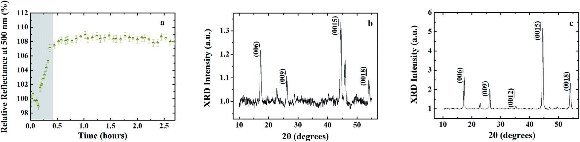 | ||
| Fig. 1 (a) Relative reflectivity at 500 nm as a function of the annealing time. (b) XRD diagram of the laser annealed sample. (c) XRD diagram of the oven annealed sample. | ||
UV-Vis spectrophotometric studies have been additionally performed for all the annealed and amorphous samples. Moreover, the refractive indices have been determined by using a single oscillator using the Drude modified Forouhi–Bloomer model. The spectra and the refractive index values have been found to be in very good agreement with previous results reported by our group.21
X-Ray diffraction (XRD) studies were then performed for the crystallized samples. Representative XRD diagrams can be seen in Fig. 1(b and c) for the laser annealed and oven annealed samples respectively. These results are in very good accordance with previous crystallographic studies of the Sb2Te3 material.21,24–26 The difference of the peak amplitudes is attributed to the different annealing surfaces. In the case of oven annealing the whole sample surface was annealed, while in the case of laser annealing a surface area of approximately 1 cm2 was crystallized. The positions of the diffraction peaks are very similar in both cases, indicating very similar crystalline structures. The main peaks of XRD diagrams are attributed to the Sb2Te3 rhombohedral structure, with a 00l preferred orientation.21,27 The additional peaks appearing at about 22.8 and 45.9 degrees, the latter only in the case of laser annealing, can probably be attributed to Te.28 This difference does not seem to affect the NLO response, which has been found to be very similar for both annealing procedures.
The NLO response of the samples was measured by means of the Z-scan technique29,30 (Fig. S4 and short description in the ESI†), employing 600 fs laser pulses using IR (1030 nm) and visible (515 nm) laser excitation with a 10 Hz repetition rate. The nonlinear refraction of the thin films studied in this work has been found to be negligible compared with the nonlinear absorption under the same experimental conditions. In Fig. 2 representative “open aperture” Z-scan curves for the oven annealed films using 1030 nm and 515 nm laser excitation wavelengths are presented. Similar results have been obtained in the case of the laser annealed samples (Fig. S5†). The amorphous samples exhibited negligible NLO responses under the same experimental conditions. Thorough measurements were performed in order to verify that no modification of the thin films was induced during the Z-scan studies. This has been achieved by performing studies in a large range of intensities (0.1 GW cm−2 to 2.5 GW cm−2) and in many different sample positions, in order to confirm excellent repeatability (Fig. S6 and S7†).
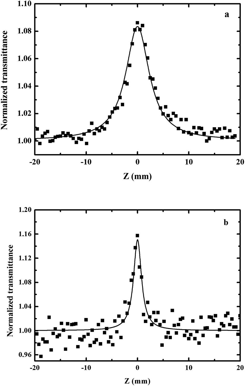 | ||
| Fig. 2 Representative “open-aperture” Z-scan curves obtained for the oven annealed samples using 600 fs laser pulses at (a) 1030 nm, I = 2 GW cm−2 and (b) 515 nm, I = 2 GW cm−2. | ||
As it can be seen in Fig. 2, a transmission maximum was obtained in all cases around the focal plane, which is due to the strong saturable absorption (SA) character of the thin films. The nonlinearities obtained in this work emanate from the topological insulator-type character of Sb2Te3. Indeed, Sb2Te3 is well-known to have insulating states in the bulk and “graphene-like” conducting states at its surface. The bleaching of the absorption, which results in a SA attribute, is caused by the Pauli blocking principle.31
The “open-aperture” Z-scans obtained in this work have been analyzed using previously published procedures.28 The nonlinear absorption coefficient and the imaginary part of the third order nonlinear optical susceptibility (Imχ(3)) have been determined by many experimental curves and are presented in Table 1 in the case of the oven and laser annealed samples. The obtained values are of the order of β ∼ 105 cm GW−1 and Imχ(3) ∼ 10−7 esu. These values are the highest ever reported by the Z-scan technique for a saturable absorber. No evidence of nonlinear refraction has been obtained during our measurements. We estimate that the real part of the third order nonlinear optical susceptibility (Reχ(3)) is at least one order of magnitude lower than the imaginary part (Imχ(3)), under the same experimental conditions. In Table 1, a comparison with other state-of-the-art materials is done. The NLO parameters reported here are about one order of magnitude higher compared with a previous study for Sb2Te3.20 They are also 2–4 times higher than those reported for 2D α-Mo2C crystals,32 GeSb4Te7,33 and carbon nanotubes,3 5 times to more than one order of magnitude compared with those of Bi2TexSe3−x materials,34 2–4 orders of magnitude higher than the NLO responses reported for graphene and graphene oxide4,35,36 and 2–3 orders of magnitude higher than those of black phosphorus.37 The NLO parameters measured in this work are about 6 orders of magnitude higher than those of CsPbBr3 perovskite quantum dots6 and 2 orders of magnitude higher than those of MAPbI3 perovskites5 and CH3NH3PbI3 perovskite nanosheets.38 Nonlinear optical parameters of the same order of magnitude with those reported here have been found by Zhang et al.39 in the case of Bi2Se3. However the authors employ a different experimental technique (micro P-scan) so a further comparison of the performances is not feasible. Similar values with those found here have been reported by Abdelwahab et al. in the case of single-crystalline 2D perovskites, however, in that case a tuning of the excitation wavelength was necessary.40 On the contrary, the findings reported here show that large values can be obtained for Sb2Te3 thin films both in the visible and the IR parts of the spectrum. The broadband NLO character of the thin films optimized in this work reveals a significant advantage of the Sb2Te3 material.
| Material | Experimental parameters | β [cm GW−1] | Imχ(3) [×10−11 esu] | Ref. |
|---|---|---|---|---|
| Bi2Se3 | 800 nm, 1 kHz, 65 fs | −596![[thin space (1/6-em)]](https://www.rsc.org/images/entities/char_2009.gif) 980 980 |
N/A | 39 |
| Sb2Te3 (oven annealing) | 515 nm, 10 Hz, 600 fs | −380000 |
−15000 |
This work |
| Sb2Te3 (laser annealing) | 515 nm, 10 Hz, 600 fs | −340000 |
−14000 |
This work |
| (BA)2(MA)Pb2I7 | 570 nm, 150 fs | −256000 |
N/A | 40 |
| Sb2Te3 (oven annealing) | 1030 nm, 10 Hz, 600 fs | −200000 |
−39000 |
This work |
| Sb2Te3 (laser annealing) | 1030 nm, 10 Hz, 600 fs | −200000 |
−39000 |
This work |
| 2D α-Mo2C | 1550 nm, 2 kHz | −100000 |
N/A | 32 |
| GeSb4Te7 | 800 nm, 1 kHz, 100 fs | −93009 |
N/A | 33 |
| Carbon nanotubes | 1300 nm, 1 kHz, 200 fs | N/A | −8500 | 3 |
| Bi2Se3 | 800 nm, 2 kHz, 35 fs | −65000 |
−1770 | 34 |
| Bi2Te3 | 1050 nm, 2 kHz, 35 fs | −47000 |
−1720 | 34 |
| Sb2Te3 | 800 nm, 1 kHz, 100 fs | −37100 |
N/A | 20 |
| WS2 | 515 nm, 1 kHz, 340 fs | −29000 |
−8440 | 41 |
| Bi2Te2Se | 1050 nm, 2 kHz, 35 fs | −25000 |
−930 | 34 |
| Bi2TeSe2 | 1050 nm, 2 kHz, 35 fs | −24000 |
−870 | 34 |
| Black phosphorus | 1160 nm, 65 fs | −6980 | −4340 | 37 |
| CH3NH3PbI3 | 800 nm, 80 MHz, 140 fs | −1934 | N/A | 38 |
| MAPbI3 | 514 nm, 1 kHz, 200 fs | −1500 | N/A | 5 |
| MoS2/graphene | 800 nm, 1 kHz | −1217.76 | −320 | 36 |
| Graphene | 800 nm, 1 kHz | −961.57 | −240 | 36 |
| WS2 | 800 nm, 1 kHz, 40 fs | −397 | −178 | 41 |
| MoS2 | 1030 nm, 1 kHz, 340 fs | −250 | −150 | 41 |
| MoS2 | 800 nm, 1 kHz | −136.13 | −30 | 36 |
| Graphene | 790 nm, 1 kHz, 80 fs | −90 | N/A | 4 |
| Graphene oxide | 790 nm, 1 kHz, 80 fs | −40 | N/A | 4 |
| CsPbBr3 | 515 nm, 1 kHz, 340 fs | −0.35 | N/A | 6 |
Conclusions
In summary, precise crystallization of Sb2Te3 thin films has been performed in order to enhance the optical nonlinearities in the IR and visible parts of the spectrum. Large nonlinear absorption coefficients are obtained (∼105 cm GW−1), which are the highest values ever obtained for a saturable absorber, by means of the Z-scan technique. These results show that this material is a very high performance saturable absorber in the ultrafast regime. The process followed here in order to enhance the optical nonlinearities provides a reference for several fields of photonics, such as mode-locking and super-resolution.Conflicts of interest
There are no conflicts of interest to declare.Acknowledgements
This work was supported by the Region PACA (Project: APEX 2017 NANOFAB). The authors also acknowledge support from the Ministry of Armed Forces (DGA) and Aix-Marseille University.References
- J. Xu, X. Li, J. Xiong, C. Yuan, S. Semin, T. Rasing and X. Bu, Adv. Mater., 2019, 1806736 Search PubMed.
- D. Mao, B. Du, D. Yang, S. Zhang, Y. Wang, W. Zhang, X. She, H. Cheng, H. Zeng and J. Zhao, Small, 2016, 12, 1489–1497 CrossRef CAS PubMed.
- S. Tatsuura, M. Furuki, Y. Sato, I. Iwasa, M. Tian and H. Mitsu, Adv. Mater., 2003, 15, 534–537 CrossRef CAS.
- S. Kumar, M. Anija, N. Kamaraju, K. S. Vasu, K. S. Subrahmanyam, A. K. Sood and C. N. R. Rao, Appl. Phys. Lett., 2009, 95, 191911 CrossRef.
- B. S. Kalanoor, L. Gouda, R. Gottesman, S. Tirosh, E. Haltzi, A. Zaban and Y. R. Tischler, ACS Photonics, 2016, 3, 361–370 CrossRef CAS.
- J. Li, H. Dong, B. Xu, S. Zhang, Z. Cai, J. Wang and L. Zhang, Photonics Res., 2017, 5, 457–460 CrossRef CAS.
- J. Lee, M. Tymchenko, C. Argyropoulos, P.-Y. Chen, F. Lu, F. Demmerle, G. Boehm, M.-C. Amann, A. Alù and M. A. Belkin, Nature, 2014, 511, 65–69 CrossRef CAS PubMed.
- T. D. James, P. Mulvaney and A. Roberts, Nano Lett., 2016, 16, 3817–3823 CrossRef CAS PubMed.
- R. Mudachathi and T. Tanaka, Sci. Rep., 2017, 7, 1999 CrossRef PubMed.
- N. Yu and F. Capasso, Nat. Mater., 2014, 13, 139–150 CrossRef CAS PubMed.
- K. Iliopoulos, O. Krupka, D. Gindre and M. Sallé, J. Am. Chem. Soc., 2010, 132, 14343–14345 CrossRef CAS PubMed.
- M. Beresna, M. Gecevičius and P. G. Kazansky, Adv. Opt. Photonics, 2014, 6, 293–339 CrossRef.
- S. Juodkazis, V. Mizeikis, K. K. Seet, M. Miwa and H. Misawa, Nanotechnology, 2005, 16, 846–849 CrossRef CAS.
- R. Wollhofen, J. Katzmann, C. Hrelescu, J. Jacak and T. A. Klar, Opt. Express, 2013, 21, 10831–10840 CrossRef CAS PubMed.
- J. Wei, S. Liu, Y. Geng, Y. Wang, X. Li, Y. Wu and A. Dun, Nanoscale, 2011, 3, 3233–3237 RSC.
- Z. Luo, Y. Huang, J. Weng, H. Cheng, Z. Lin, B. Xu, Z. Cai and H. Xu, Opt. Express, 2013, 21, 29516–29522 CrossRef PubMed.
- H.-R. Chen, C.-Y. Tsai, H.-M. Cheng, K.-H. Lin, P.-H. Yen, C.-H. Chen and W.-F. Hsieh, Sci. Rep., 2016, 6, 38444 CrossRef CAS PubMed.
- Z. Wang, C. Li, J. Ye, Z. Wang and Y.-G. Liu, Laser Phys. Lett., 2019, 16, 025103 CrossRef CAS.
- M. Kowalczyk, J. Bogusławski, R. Zybała, K. Mars, A. Mikuła, G. Soboń and J. Sotor, Opt. Mater. Express, 2016, 6, 2273 CrossRef CAS.
- C. Liu, L. Cheng, Y. Yuan, J. Su, X. Zhang, X. Li, H. Zhao, H. Zhang, Y. Zheng and J. Li, Mater. Res. Express, 2019, 6, 086446 CrossRef CAS.
- C. Moisset, A. Bourgade, J. Lumeau, F. Lemarchand, C. Perrin-Pellegrino, H. Akhouayri, J.-Y. Natoli and K. Iliopoulos, Opt. Mater., 2018, 86, 7–11 CrossRef CAS.
- M. Minissale, C. Pardanaud, R. Bisson and L. Gallais, J. Phys. D: Appl. Phys., 2017, 50, 455601 CrossRef.
- S. Fujimori, S. Yagi, H. Yamazaki and N. Funakoshi, J. Appl. Phys., 1988, 64, 1000–1004 CrossRef CAS.
- Q. Wang, B. Liu, Y. Xia, Y. Zheng, R. Huo, M. Zhu, S. Song, S. Lv, Y. Cheng, Z. Song and S. Feng, Phys. Status Solidi RRL, 2015, 9, 470–474 CrossRef CAS.
- Y. Yin, H. Sone and S. Hosaka, J. Appl. Phys., 2007, 102, 064503 CrossRef.
- T. Liu, H. Deng, H. Cao, W. Zhou, J. Zhang, J. Liu, P. Yang and J. Chu, J. Cryst. Growth, 2015, 416, 78–81 CrossRef CAS.
- PDF # 01-072-1990; ICDD, 2002.
- PDF # 00-036-1452; ICDD, 2002.
- M. Sheik-Bahae, A. A. Said, T.-H. Wei, D. J. Hagan and E. W. Van Stryland, IEEE J. Quantum Electron., 1990, 26, 760–769 CrossRef CAS.
- K. Iliopoulos, A. El-Ghayoury, H. El Ouazzani, M. Pranaitis, E. Belhadj, E. Ripaud, M. Mazari, M. Sallé, D. Gindre and B. Sahraoui, Opt. Express, 2012, 20, 25311–25316 CrossRef CAS PubMed.
- P. Loiko, J. Bogusławski, J. M. Serres, E. Kifle, M. Kowalczyk, X. Mateos, J. Sotor, R. Zybała, K. Mars, A. MikuŁa, K. Kaszyca, M. Aguiló, F. Díaz, U. Griebner and V. Petrov, Opt. Mater. Express, 2018, 8, 1723–1732 CrossRef CAS.
- M. Tuo, C. Xu, H. Mu, X. Bao, Y. Wang, S. Xiao, W. Ma, L. Li, D. Tang, H. Zhang, M. Premaratne, B. Sun, H.-M. Cheng, S. Li, W. Ren and Q. Bao, ACS Photonics, 2018, 5, 1808–1816 CrossRef CAS.
- J. Fang, J. Wang, X. Cao, Y. Man, C. Liu, L. Cheng, X. Zhang, H. Zhao, H. Zhang and J. Li, J. Phys. Commun., 2018, 2, 015009 CrossRef.
- Y. Wang, S. Liu, J. Yuan, P. Wang, J. Chen, J. Li, S. Xiao, Q. Bao, Y. Gao and J. He, Sci. Rep., 2016, 6, 33070 CrossRef CAS PubMed.
- Y. Jiang, Y. Ma, Z. Fan, P. Wang, X. Li, Y. Wang, Y. Zhang, J. Shen, G. Wang, Z.-J. Yang, S. Xiao, Y. Gao and J. He, Opt. Lett., 2018, 43, 523–526 CrossRef CAS PubMed.
- M. He, C. Quan, C. He, Y. Huang, L. Zhu, Z. Yao, S. Zhang, J. Bai and X. Xu, J. Phys. Chem. C, 2017, 121, 27147–27153 CrossRef CAS.
- R. Chen, Y. Tang, X. Zheng and T. Jiang, Appl. Opt., 2016, 55, 10307–10312 CrossRef CAS PubMed.
- P. Li, Y. Chen, T. Yang, Z. Wang, H. Lin, Y. Xu, L. Li, H. Mu, B. N. Shivananju, Y. Zhang, Q. Zhang, A. Pan, S. Li, D. Tang, B. Jia, H. Zhang and Q. Bao, ACS Appl. Mater. Interfaces, 2017, 9, 12759–12765 CrossRef CAS PubMed.
- J. Zhang, T. Jiang, T. Zhou, H. Ouyang, C. Zhang, Z. Xin, Z. Wang and X. Cheng, Photonics Res., 2018, 6, C8–C14 CrossRef CAS.
- I. Abdelwahab, P. Dichtl, G. Grinblat, K. Leng, X. Chi, I. Park, M. P. Nielsen, R. F. Oulton, K. P. Loh and S. A. Maier, Adv. Mater., 2019, 31, 1902685 CrossRef PubMed.
- S. Zhang, N. Dong, N. McEvoy, M. O'Brien, S. Winters, N. C. Berner, C. Yim, Y. Li, X. Zhang, Z. Chen, L. Zhang, G. S. Duesberg and J. Wang, ACS Nano, 2015, 9, 7142–7150 CrossRef CAS PubMed.
Footnote |
| † Electronic supplementary information (ESI) available. See DOI: 10.1039/c9na00796b |
| This journal is © The Royal Society of Chemistry 2020 |