
 Open Access Article
 This Open Access Article is licensed under a
 Creative Commons Attribution 3.0 Unported Licence
Metal/semiconductor interfaces in nanoscale objects: synthesis, emerging properties and applications of hybrid nanostructures
Michael
Volokh
 and
Taleb
Mokari
*
and
Taleb
Mokari
*
Department of Chemistry, Ilse Katz Institute for Nanoscale Science and Technology, Ben-Gurion University of the Negev, Beer-Sheva 8410501, Israel. E-mail: mokari@bgu.ac.il
First published on 2nd March 2020
Abstract
Hybrid nanostructures, composed of multi-component crystals of various shapes, sizes and compositions are much sought-after functional materials. Pairing the ability to tune each material separately and controllably combine two (or more) domains with defined spatial orientation results in new properties. In this review, we discuss the various synthetic mechanisms for the formation of hybrid nanostructures of various complexities containing at least one metal/semiconductor interface, with a focus on colloidal chemistry. Different synthetic approaches, alongside the underlying kinetic and thermodynamic principles are discussed, and future advancement prospects are evaluated. Furthermore, the proved unique properties are reviewed with emphasis on the connection between the synthetic method and the resulting physical, chemical and optical properties with applications in fields such as photocatalysis.
1. Introduction
Today, different nano-sized objects are synthesized, manipulated, characterized, and utilized in a plethora of scientific and technological applications. Every B.Sc. student in chemistry, physics, and most branches of engineering has heard of ‘nano’ objects such as carbon nanotubes or quantum dots (QD). Colloidal QDs are considered a masterpiece of modern nanoscience. The development of the hot-injection method1 in 1993 allowed studying the unique optical properties of QDs, since the surfactant-assisted precision synthetic method gives controlled surface chemistry with narrow size distributions and uniform morphologies.2 The QD, which is a quantum-confined semiconductor nanocrystal, is just one excellent example of the rapid progress of this relatively new field of science, from the theoretical description of quantum-confinement, which explains the unique photophysical properties, to other calculated physical properties,3 through different applications in electronic and optoelectronic devices,4 to commercialization in displays and bio-labeling, which are already on the market.5With available pathways for the controlled synthesis of various shapes, sizes, and compositions of nanoscale objects (see for example reviews by van Embden et al.6 and Hyeon and co-workers7–9 on various colloidal synthetic methods), scientists looked for ways to combine two (or more) nano-objects into hybrid nanostructures (HNS) and potentially obtain materials with new properties. Continuing with the QD example, varying the deposition of a second semiconductor crystal on the existing QD results in a hybrid semiconductor/semiconductor (SC/SC) interface; some synthesized examples include core/(multi)shell,10–18 yolk/shell19–21 and heterodimers (usually two or more quasi-spherical shapes forming a heterojunction22–24 as well as acorn-style structures25). When the QD serves as a seed for an anisotropic structure such as a rod,26 tetrapod26,27 or octapod,28 more complex structures result,29 where the seed (junction) and arm are different SCs. Obviously, if the starting material is anisotropic (e.g., nano-rod, -wire, -belt, -ribbon, -sheet, -pyramid)6,30,31 or even branched,32 other hybrid SC/SC nanostructures (possibly with mixed dimensionalities) result—ranging from simple heterostructures through rod-in-rod, dumbbells, dot-in-rod and graded shells,33 to ‘double’ QD fixed in a rod with unique optoelectronic properties.34 The examples thus far focused on the SC/SC interface, but a vast body of knowledge has been acquired on interfacing a SC with a metal (M)—these hybrid nanostructures (HNSs) are the topic of this review—and we will begin with discussion of binary systems in Section 2. For detailed analysis of the electronic coupling between a semiconductor, a metal and variable (insulating) interfaces, we refer the reader to the thorough review by Vilan and Cahen.35
Both shape and size dictate the electronic structure in metals36 and in semiconductors due to different quantum-confinement effects.37 Noteworthy, many electronic and optical properties of nanocrystals result not only from dimensionality and size but also from surface properties.38 Formation of an HNS could result in a mere combination of the individual material's properties (fluorescence, magnetism, plasmonic response, catalytic activity and so forth). However, usually, new properties arise from both the modifications at the surface of the original constituents and the newly formed interface, ranging from inherent physical properties to functional applications such as controlled self-assembly into superlattices without the inherent anisotropy of the HNS.39 The main criterion of distinction between the various possible nanohybrids is the type of the interface present: SC/SC,16 M/M,40 and M/SC.41,42 For practical applications such as photocatalysis, multiple interfaces can also be combined.43
In this review, we focus on the tremendous synthetic progress achieved in the formation of hybrid inorganic M/SC nanostructures and their interfaces, mainly in colloidal liquid-phase syntheses. The building blocks of HNSs are commonly referred to as nanocrystals (NCs) and nanoparticles (NPs), with NCs usually referring to a semiconductor and NPs—despite being a general term—usually implies a metallic nano-object. Since the chemical principles of nanoscale synthesis have been reviewed,44 we will emphasize the mechanisms of growth and precise control over the formed interfaces between metals and semiconductors (with a special focus on the II–VI family—the metal-chalcogenide (O, S, Se, Te) materials and formation of anisotropy or asymmetry). We refer the reader to excellent reviews by Cozzoli and co-workers,45,46 Manna and co-workers,47 and Banin and co-workers,48 who set the groundwork for the description of hybrid nanostructures, and a recent review from Zhang and co-workers on epitaxial multicomponent HNSs.49 These studies give a broad overview of the development of the field and various possible interfaces that can form alongside thermodynamic requirements for the growth of HNSs. Having this knowledge at the reader's disposal allows us to select illustrative HNS examples (including knowledge accumulated in our group) to elaborate the chemical principles of colloidal metal–semiconductor HNS synthesis, and explore new synthetic approaches for the formation of HNSs with increasing complexity (Section 3), which were developed during the last decade such as using a total-synthesis framework for formation of high-order hybrid nanoparticles, developed by Schaak and co-workers.50,51
Furthermore, we mention in Section 2.2 additional non-semiconductor transition metal–nonmetal compounds, which have many synthetic similarities to semiconductors and can form during HNS synthesis. Finally, we demonstrate how the new emergent properties of the various HNSs are beneficial in selected applications, such as (photo)catalysis (Section 4).
2. Formation of binary metal/semiconductor hybrid nanostructures
Discussing M/SC interfaces raises several interesting scientific questions. What is the mechanism behind the possibility of forming an intimate interface between two different (ordered) materials? What keeps the final structure stable? What are the underlying thermodynamic, kinetic and mechanistic principles (and details) that are responsible for the intermediate steps of the reaction? What is the interplay between the chosen precursors and the required external energy source (photons, electrons, thermal energy, electrochemical potential, etc.) required to drive the reaction forward? What are the effects of the size and shape of the domains and the interface on the possible structures? And finally, which new phenomena arise from the successful formation of the hybrid at the nanoscale?With these scientific questions in mind, a simplified M/SC HNS application-oriented design scheme may be proposed: (i) determine the relevant properties of the individual metal and semiconductor domains; (ii) specify the physical, mechanical, chemical, optical or electronic properties that are expected to change or remain unaltered after the hybrid structure has been synthesized; (iii) verify that the property-combination is suitable for the potential applications. Once decided, the most-suitable synthetic procedure can be designed. Our goal in this review is to give an overview of the most up-to-date answers to the chemistry-of-materials questions, with a focus on the synthetic possibilities.
It is impossible to provide an adequate classification of all possible property combinations, yet a useful generalization would be to classify the metal and semiconductor roles. The intrinsic role of a metal (or a bimetallic compound) can be classified, as common for metal NPs,52 into plasmonic (e.g., Cu, Ag, Au), magnetic (Fe, Ni, Co), and catalytic properties (e.g., Pt-group metals). To these roles, we can add the electronic properties of the metal, which are intimately connected to the semiconductor—specifically, electrical conductivity and Fermi level (EF). In the case of the semiconductor, the most important property is usually the bandgap (Eg), which defines the material and its optical absorption, though the entire electronic structure (i.e., density of states) is important for planning an applicable M/SC interface: Fermi level, doping, band positions and expected defect levels, carrier diffusion length, fluorescence yield and even plasmonic response due to defects in semiconductors (e.g., vacancies in copper sulfide and impurity doping in metal oxides).53
2.1 Colloidal routes to form M/SC interfaces
In the colloidal synthesis realm, nanocrystals either crystallize on predetermined sites or form in a solution due to a nucleation event. Since homogeneous nucleation is less favorable than heterogeneous nucleation on a pre-existing nucleation site, the planned placement of nucleation sites allows the synthesis of complicated nanostructures in a variety of techniques. The same considerations apply during the growth of a material—the free energy barrier is lower for the nucleation of a precursor on an existing crystal than for spontaneous homogeneous nucleation.This basic thermodynamic principle,54 alongside kinetic control over the number of available nucleation sites and precursors, allows interfacing two materials. Fig. 1 schematically depicts the conventional two-step approaches for the formation of SC/M and M/SC interfaces. One can divide the syntheses according to the first material employed: semiconductor or metal. When the first material is a semiconductor, the subsequent metal domain formation is usually performed by reducing a metal cation—either using a photo-assisted process (Section 2.1.1) or chemically (Section 2.1.2). This is approach (I), where a reduction of metal from the solution results in nucleation and growth on the SC. The other option, approach (II), is a partial chemical reduction of the SC at the surface of the nanocrystal, resulting in metal coating or domains. This is a relatively rare synthetic approach with a starting SC (e.g., Cu2O into Cu2O/Cu0).55
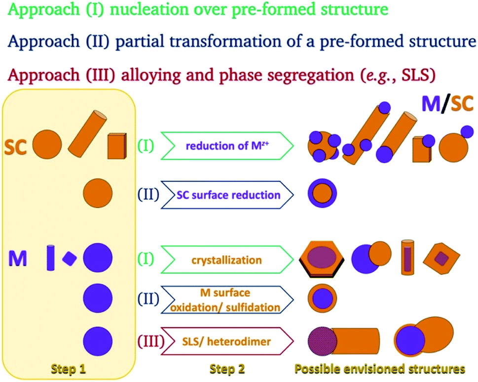 | ||
| Fig. 1 Schematic options to form nanoscale colloidal-phase heterostructures using a starting semiconductor (SC, orange) or metal (M, purple) structure. Approach (I): nucleation of M over SC or SC over M; approach (II): partial transformation of the first structure (reduction at the surface of a binary SC's cation to the metal or surface transformation of a metal into a semiconductor (e.g., oxidation or sulfidation)); approach (III): precipitation out of a metal-alloy core, which either forms a heterodimer or a nanorod via a solid–liquid–solid (SLS) mechanism, where the SC precursors are dissolved in the metal tip (alloying) and precipitate out of it, resulting in the formation of an M/SC interface. | ||
The colloidal approaches for the synthesis of metal NPs (as the anchor for a subsequent SC growth) are dominated by chemical reduction both in aqueous and organic-solvent environments. The most prominent example is the citrate-assisted reduction of gold from Au(III) to Au0, but alcohols, amines,56etc. are also common reducing agents. Noticeable alternatives include the use of metal carbonyl complexes, where the metal's oxidation state is 0.57 To stabilize the resulting metallic NPs, the typical surfactants are long-chain organic molecules, polymers (e.g., PVP), and micelles (formed using hexadecyl-trimethyl-ammonium bromide, CTAB, in an aqueous environment for example).
The metal can serve as the seed for growth of SC crystals (approach (I), discussed in Section 2.1.3), as the substrate for chemical transformations (approach (II), e.g., surface oxidation and sulfidation, discussed in Section 2.1.4), or as the catalyst for a solution–liquid–solid (SLS) growth (approach (III), Section 2.1.5).
![[thin space (1/6-em)]](https://www.rsc.org/images/entities/char_2009.gif) :1 v/v) mixture.58 Alivisatos and co-workers have shown photodeposition of Pt on CdS and CdSe–CdS core–shell NRs in toluene.59 The control over the number of Pt NPs per rod (a wide distribution in the 0–6 range) proved to be hard, with the best control achieved on well-passivated CdSe–CdS NRs, where most NRs contained a single Pt domain, close to the CdSe core. Others have deposited different metals on various semiconductors of diverse shapes.60 Recently, photodeposition in ionic liquids has been carried out by Hill and co-workers, who have shown non-selective deposition of Pt, Au and Ag on CdSe–CdS NRs with similar results to the common amine-capped colloidal synthesis in toluene (Fig. 2a).61
:1 v/v) mixture.58 Alivisatos and co-workers have shown photodeposition of Pt on CdS and CdSe–CdS core–shell NRs in toluene.59 The control over the number of Pt NPs per rod (a wide distribution in the 0–6 range) proved to be hard, with the best control achieved on well-passivated CdSe–CdS NRs, where most NRs contained a single Pt domain, close to the CdSe core. Others have deposited different metals on various semiconductors of diverse shapes.60 Recently, photodeposition in ionic liquids has been carried out by Hill and co-workers, who have shown non-selective deposition of Pt, Au and Ag on CdSe–CdS NRs with similar results to the common amine-capped colloidal synthesis in toluene (Fig. 2a).61
 | ||
| Fig. 2 Examples of metal photodeposition on SCs. (a) Pt/CdSe–CdS NRs via a non-selective Pt domain photodeposition reaction carried out in an ionic liquid, adapted from ref. 61, Creative Commons Attribution 4.0 International Public License, published by Beilstein-Institut, copyright 2019. (b) Ni/CdS NCs, adapted with permission from ref. 67, American Chemical Society, copyright 2016. (c) Ni/CdS nanosheets, adapted with permission from ref. 68, American Chemical Society, copyright 2015. | ||
Carbone et al. have used UV light in 9:1 v/v CHCl3:ethanol (EtOH) to achieve controlled reduction of gold on the tips of CdS and CdSe(core)@(shell)CdS NRs.62 The advantage of this method is that the EtOH acts as an electron donor, reacting with the photogenerated holes in the semiconductor, thus allowing the photogenerated electron in the rod to reduce a gold cation. This method allowed the synthesis of large Au domains on CdSe@CdS or CdS NR tips and nano-dumbbells. The fact that the large domain formation is selective at one tip is a significant synthetic achievement since photodeposition is not usually selective. By measuring the absorption peak location stemming from the metal domain's plasmonic response, transmission electron microscopy (TEM) analysis and controlled addition of a gold precursor, the authors deduce that the mechanism is mainly through selective drift of the photogenerated electrons towards the gold tip (forming, at first, alongside other Au domains), which enhances further reduction of the large metal tip, acting as an electron sink.
Fernando et al. have shown that gold readily photodeposits on ZnO at high-energy sites as facet edges and corners when the capping ligand is a labile amine, but when a more strongly bound dodecanethiol (DDT) is used, the deposition is quenched.63 Furthermore, since the deposition rate depends on the interfacial electron transfer from the ZnO to the cationic gold complex, changing the solvent could determine whether multiple small Au domains are formed, or fewer larger Au clusters result (when the reaction conditions favor charge accumulation).63 The main drawback of the photodeposition approach discussed thus far is its non-selective nature. This work also demonstrates another limitation, which is the non-epitaxial nature of the formed heterostructure.63 In a successive study, it was demonstrated that a sequential photodeposition of Pt over photodeposited Au/ZnO HNS results in a non-selective Pt deposition with Pt and Au domains distributed over the ZnO core, while changing the procedure to Pt photodeposition on an Au-seeded/ZnO HNS (the focus of Section 2.1.3) allows selective deposition of Pt on the existing epitaxial Au domains/ZnO.64
In aqueous solutions, when TiO2 NPs are illuminated using UV radiation in the presence of KMnO4, the reduction results in the formation of a TiO2/MnO2 HNS with manganese oxide domains. As most domains are present on one side, a Janus particle is formed, which can catalytically decompose H2O2 as a proof-of-concept ‘nanomotor’.65 Another example is a CdS–nickel oxide hybrid, which consists mostly of Ni2O3, which is photodeposited using UV irradiation in an aqueous environment containing Ni2+ salt and nitrites.66 These two examples demonstrate that metal-oxides and -hydroxides are easily formed in aqueous environments.
Partial oxidation of Ni in CdS/Ni HNSs due to the presence of water was suggested by Chai et al. to be responsible for less efficient photocatalytic dehydrogenation of alcohols—for this reason, they performed the Ni photodeposition in methanol (Fig. 2b).67 Simon et al., managed to synthesize multiple decorating elemental Ni NPs on a cysteine-stabilized aqueous colloid of CdS NRs by photodeposition with low amounts of NiO and Ni(OH)2.69 They ascribe this success to surface-trapped photoexcited electrons, which reduce the nickel cations in their vicinity; once a metallic cluster is formed, it serves as an electron sink to further reduce and form Ni NPs with diameters of about 5 nm (though 2 nm NPs were also detected). Kuno and co-workers selectively deposited Ni on 2D CdS nanosheets in an Ar-purged 10% EtOH aqueous solution under 405 nm laser illumination (Fig. 2c).68 Mahler and co-workers used photo-assisted reduction to form large Au domains on 2D CdSe/CdZnS.70
Another innovative use of photoexcitation in HNSs is the transformation of a CdS NR/Pt tip into copper-deficient Cu2S NR/Pt using light-induced cation exchange in an aqueous environment as demonstrated by Manzi et al. for CO2 reduction applications.71
Further investigation of a similar system of CdS NRs showed an interesting strategy to control the amount and location of the gold NPs—the reduction takes place on defect sites at the nanorod's surface, thus controlled etching allowed exposing more defect sites.75Fig. 3 presents this trend of increasing surface decoration with Au NPs. In the presence of air and trace amounts of water, etching of the NR provides additional nucleation sites for the metal, resulting in multiple non-epitaxial gold domains. Without exposure to air, only a single tip forms; with air, Au/CdS heterostructures are formed on both tips resulting in hybrid nano-dumbbells at reaction times < 90 min (panel e, Fig. 3); longer reaction times result in growth throughout the rod. An important consequence of even longer reaction times is a ripening process, where small Au domains dissolved back into the solution and were redeposited on the tip, leading to a single large Au tip.75
 | ||
| Fig. 3 Gold decoration of CdS NRs (average dimensions 3.9 × 100 nm) with and without exposure to air. (a) Deaerated synthesis results in no gold deposition; (b) at the initial stage (∼30 min), gold nucleates preferentially on the NRs' tips; (c) after 150 min, considerable gold growth on defect sites along the NRs; (d) after long reaction times (3 days), large gold domains are formed via a ripening mechanism, i.e., large domains are formed at the expense of small NPs, which have a higher tendency to dissolute. (e) Gold nucleation on CdS NRs with a smaller aspect ratio (3.9 × 20 nm) after ca. 80 min. (f) The corresponding histograms of Au domain diameters: size evolution over time for images (b–d). Reproduced from ref. 75 with permission from the American Chemical Society, copyright 2006. | ||
Using a similar procedure with a platinum source does not work. To achieve selective Pt-tipped CdS NRs, a combination of oleic acid (OA), oleylamine (OY) and 1,2-hexadecanediol in diphenylether is used. 10 min at 65 °C is sufficient to allow dissolution of the Pt acetylacetonate (Pt(acac)2) precursor, which is then injected at 200 °C into the CdS NR mixture.76
This procedure, adapted from a NixPt1−x synthesis,77 also allowed the formation of bimetallic tips (i.e., PtCo and PtNi) when the other metal precursors are present in the system prior to injection.76,78 The choice of stabilizers is responsible for the metal (or bimetallic) tip—with the OA:OY combination being responsible for the spherical single-crystalline nature while the diol is mainly responsible for the reduction. Schlicke et al. have shown that a Pt-tipped CdS NR can be transformed in a subsequent step into a faceted metallic tip, by introduction of CO(g) to the growth solution in benzyl ether.79 The CO served a dual role—it reduced the Pt(acac)2 on the pre-formed Pt-tip and also dictated the final {100} faceted tip morphology.
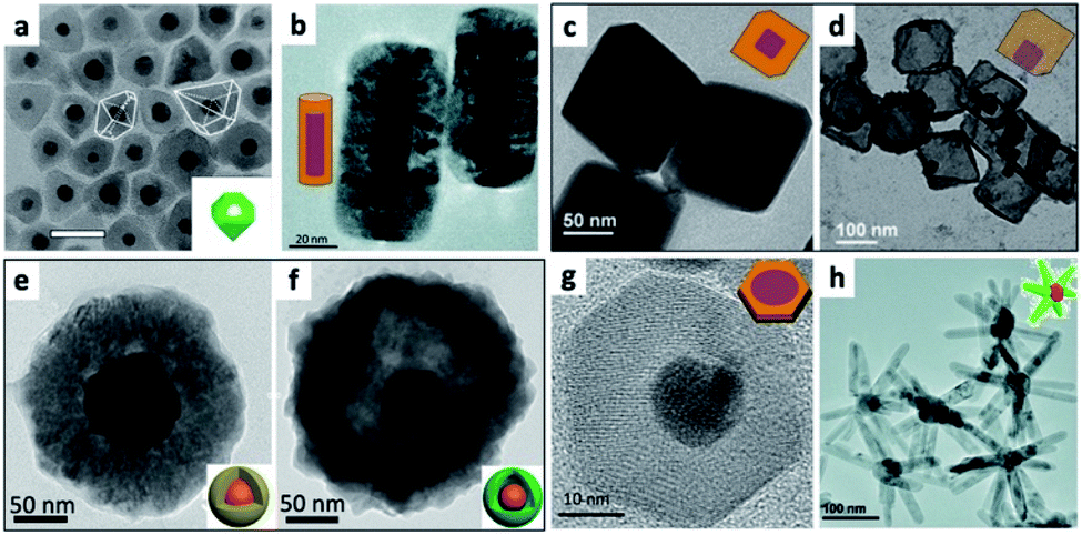
Some examples of different adaptations of the above-mentioned selective deposition methods of gold and platinum resulted in CdSe pyramids/Au,80 PbS QDs/Au,81 PbSe QDs/multiple-domain(s) and sizes of Au,82 PbTe nanocubes/Au,83 Ag2Se/Au and Ag3AuSe2/Au,84 Cu2ZnSnS4 (CZTS, a Cd-free SC with Eg ∼ 1.5 eV) cubes/Au and /Pt,85 NRs/Au,86 core@shell or heterodimers with Pt, Pd and Au,87 QDs/AuAg,88 CuInS2/Pt,89 CdSe@CdS NR/Pt,90 CdSe@CdS NR/Co,57 CdSe@CdS NR/Ni,91 Bi2S3/Au nano-dumbbells,92 anisotropic quasi-2D CdSe nanosheets or nanoplatelets (NPLs)70,93–96 and related 2D cadmium chalcogenides (e.g., CdS96,97 and CdSe–CdS core–crown NPLs94,95) with metals such as /Au,70,93–95,97 /Pt,93–97 /Pd,93 metal alloys such as Pt–Au95 and Ni–Pt,97 as well as selective deposition of distinguishable Pt and Au domains.95 The mentioned variations include changes to the shape, size, morphology and material of the starting SC, as well as expansion of the deposited metals and alloys, some of which are reproduced in Fig. 4.
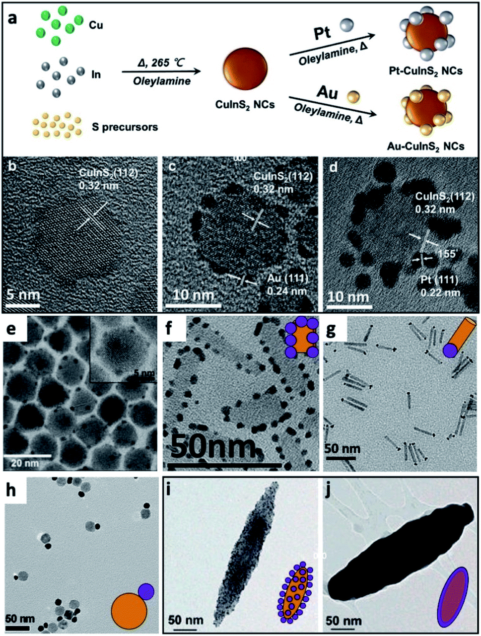 | ||
| Fig. 4 Gallery of chemical reduction and related methods of depositing metals on SCs. (a–d) Non-selective reduction of gold and platinum in the presence of OY on CuInS2 NCs, reproduced with permission from ref. 98, Wiley-VCH Verlag GmbH & Co., copyright 2019: (a) synthetic scheme, HRTEM image of (b) CuInS2 NCs, (c) Au/CuInS2 and (d) Pt/CuInS2. (e) CdSe NC/Au, where Au domains were reduced selectively on the apexes of the CdSe nanopyramids, reproduced with permission from the Royal Society of Chemistry, ref. 80 copyright 2010. (f) Pt on the edges of CdSe nanoplatelets (NPLs), adapted with permission from ref. 93, American Chemical Society, copyright 2015. (g) Selective reduction of Pt on one tip of CdS NRs, adapted with permission from the American Chemical Society, ref. 90 copyright 2016. (h) Au/Fe3O4 dimer, adapted with permission from ref. 108, American Chemical Society, copyright 2019. (i and j) Hybrid Fe2O3 ‘nanorice’ with Au NPs attached via a linker, (i) before and (j) after formation of a complete shell, adapted with permission from ref. 109, American Chemical Society, copyright 2006. | ||
A case where no selectivity is required is the deposition of multiple metal domains (such as Au and Pt) on isotropic NCs (such as CuInS2); such an example from Tang et al. is shown in Fig. 4a–d, where only OY is used for reduction of both metals, and the authors integrated this HNS into a photodetection device after forming an additional interface with MoS2.98 Other examples are deposition of 10–20 nm tin domains on CdSe 2D NPLs in tetrahydrofuran with tetrabutylammonium borohydride as the reducing agent.99 The same procedure on CdTe NPLs does not result in distinct Sn domains, but rather multiple decorations accompanied by the formation of CdSn3Te4.
An alternative to the previously described large Au-domains was reported utilizing a combination of the ‘spontaneous’ Au nucleation (chemical reduction of AuCl3 in the presence of DDAB using octadecylamine) and a second photoreduction step. The first step results in uniform single-Au-tipped HNSs, which are subsequently cleaned and redispersed under an inert atmosphere. Then, a photoreduction of Au3+ cations on the Au tips (formed at the first stage) of the HNS occurs, with the Au domains serving as the nuclei, thus preventing the deposition of gold elsewhere.100 This two-step method allows for excellent control over the size of the tips. The previously mentioned report on Au functionalization of CdSe-based NPLs from Mahler et al. also elegantly shows the benefits of choosing the reduction mechanism to control the formed domains: chemical reduction of AuCl3 in the presence of DDA and DDAB at rt results in small Au tips (<5 nm) at the edges, preferably at the corners; switching to a photo-assisted reduction, where CdSe/Cd0.5Zn0.5S NPLs are reduced in the same environment but at 0 °C and under Xe lamp illumination, results in larger 10–20 nm Au domains; Furthermore, the same procedure in the dark, but ca. 70 °C (i.e., thermal reduction) forms a large Au domain(s) (also) at the middle of the S-rich surface of the NPLs, with evidence of partial cation exchange (i.e., an Au2S phase is detected alongside the Au domain).70
Other metals such as cobalt were deposited on CdSe NRs by heating a solution of an organometallic Co-precursor in toluene in the presence of lauric acid and hexadecylamine under a reducing H2 atmosphere.101 When a multielement SC is desired, an attractive synthetic path is the use of single-source molecular precursors (SSPs), which decompose to yield, for example, tetragonal or hexagonal CuGaS2 (ref. 102) and CuGaxIn1−xSySe2−y.103 At high temperature, when the SSP decomposes, hot injection of a gold source (HAuCl4) in OY yields the SC/Au hybrid.102
An alternative approach, which circumvents using organometallic precursors is the protocol by Yang et al.,82 where different aqueous metal salt solutions are mixed with an ethanolic solution of a long chain amine (i.e., DDA), which allows transfer of the metal cation to an organic phase. They have used this to synthesize metal NPs, metal-sulfide SC nanocrystals, as well as metal-sulfide–metal HNSs. Such a multi-phase approach for metal NP synthesis has since been expanded for deposition of metals on non-sulfide-based SCs such as Pt–CeO2.104 An alternative from the Ryan group allowed controlled deposition of Au and Ag tips on Cd-chalcogenides (after sonicating their organic dispersions with octylamine and dimethylphenol, respectively) by mixing their precipitates (after centrifugation) in the respective aqueous metal-ion containing solutions, effectively inducing a phase-transfer.105 If the CdS NRs are water-soluble from the beginning, aqueous reduction of the metal is possible, as in CdS/Pt, but this approach is more suitable for coprecipitation of non-precious metal hydroxides such as CdS/Co(OH)2.106 A related mechanism involves the reduction of gold on the surface and/or edges of hydrophobic OY-capped CdSe/CdS NPLs by compression on a Langmuir–Blodget trough using an aqueous chloroauric acid subphase.107
There are also cases where a metal cation from the core can reduce a metal in its vicinity, for example, water-soluble Fe3O4 NPs in a boiling aqueous solution transform into Fe3O4/Au (shown in Fig. 4h) or /Ag, /Pd and /Pt heterodimers or metal-decorated Fe3O4 since Fe2+ on the surface can reduce Au(III) to Au(0).108
Another strategy for forming SC/M HNSs is chemical anchoring. A covalently attached molecule to the SC, with an appropriate Lewis base moiety such as an amine or sulfide, can donate its electrons to colloidal metal NPs, thus initiating a self-assembly process. This approach was used by the Halas group, for example, to attach 1–2 nm Au NPs to SiO2 cores with a 60 nm radius, treated with an organosilane (3-aminopropyltriethoxysilane), which leaves the silica spheres with outbound amines that attach to the colloidal Au NPs. As a second step, to achieve complete metal coating, further reduction by NaBH4 in the presence of chloroauric acid and potassium carbonate was used to deposit gold on and between the anchored colloidal gold particles, which serve as the seeds. These steps allow control over the shell thickness in the range between 5 and 20 nm. A similar procedure also allowed formation of water-dispersible Fe2O3 dielectric core–Au shell rice-shaped NPs (Fig. 4i and j) for investigation of plasmonic phenomena when the thicknesses of the cores and the shell are controlled (the main difference being that the reduction step was catalyzed by the Au seeds and performed using formaldehyde).109 Chang et al. used surface modification of CeVO4 nanosheets to induce a self-assembly process with a thiol (–SH) functionalization (alongside transforming the NPs into hydrophilic ones). These sites allow Ag+ ions in the solution to be directly reduced by the Ce3+, forming a CeVO4/Ag interface.110
 | ||
| Fig. 5 Examples of metals as seeds for SC overgrowth. (a) Au@NiSx core@shell HNS, reproduced from ref. 127 with permission from Elsevier, copyright 2020. (b) Au NRs@Cu2O, adapted with permission from ref. 113, the Royal Society of Chemistry, copyright 2016. (c and d) Cuprous oxide overgrowth on Pd NP cores, where the amount of reducing agent controls the polyhedron morphology, in (c) Pd@Cu2O truncated octahedron, which after addition of Na2S and acidic treatment is converted into Cu2S and partly leaches out resulting in a Pd–Cu2S yolk–shell (d), adapted with permission from the Royal Society of Chemistry, ref. 117 copyright 2013. (e and f) Cu2O overgrowth on Au by reduction of Cu2+ with hydrazine in the presence of polyvinylpyrrolidone (PVP) (e); sulfidation converts the shell into Cu9S8 and hollowing begins (f), adapted from ref. 126 with permission from Wiley-VCH Verlag GmbH & Co., copyright 2019. (g) Au/CuInS2 disc, adapted from ref. 129 with permission from the American Chemical Society, copyright 2016. (h) ZnO multipods grow out of a gold core, adapted with permission from the Royal Society of Chemistry, ref. 132 copyright 2016. | ||
The interaction of the metal core and the controlled Cu2O shell thickness are responsible for modulation of the metal plasmon position, as well as exhibiting changes to the absorption position of the cuprous oxide (a p-type direct-bandgap oxide SC, Eg = 2.17 eV).119 Shevchenko et al. have shown modulation of the Au plasmon following coating with an iron oxide shell; a similar effect was shown using a cuprous oxide shell. When an anisotropic Au NR was used as the core, not only the longitudinal but also the transverse plasmon was shifted.117
Additional optical response tuning can be achieved through formation of hollow centers in a HNS, e.g., Au@Cu2O core@shell,120 selective oxidation of Au NRs@Cu2O,121 formation of a selective gap between the outer metal core and internal Cu2O shell in Au NR@Ag@Cu2O HNSs121 and controlled formation of gaps in an Au–Cu2O yolk–shell system.122 For further information regarding the various LSPR (localized surface plasmon resonance) influences of the M–Cu2O and related M–metal oxide systems with emphasis on the facet-dependent properties we refer the reader to a review by Huang.123 On top of the tunable optical properties, these M–SC systems have potential catalytic applications, once the mechanism of electron transfer is understood. Wu and co-workers have explored the possible modes of electron transfer in Ag–Cu2O124 and in Au–Cu2O systems with a controlled silica insulating barrier layer, i.e., Au@SiO2@Cu2O.125 The increased charge-carrier generation in Cu2O stems from direct electron transfer as well as plasmon-induced resonant energy transfer.
Controlled conversion of the oxide to a sulfide results in etching of the interior part of the shell, without hurting the metal core, for example, resulting in Au NR–Cu2S and Pd–Cu2S yolk–shell HNSs117 or Au@Cu9S8 (converted from Au@Cu2O core@shell by exposure to NaHS, tested also in vivo for photoacoustic imaging and photothermal therapy, Fig. 5e and f).126
Some additional examples where a metal seed is used include: Au/NiSx where Au is the core at the center of a nickel sulfide polyhedron;127 Au/Fe7S8 NPL;128 Au/CuInS2 disc, where an epitaxial relationship was achieved by reacting Cu(acac)2 and In(acac)3 with DDT (thiolated Cu(II) and In(III) precursors) and OY in the presence of OY-capped gold seeds to first nucleate CuInS2 forming twin dots that evolved during the reaction at 200 °C to an epitaxial 0D fcc (cubic) gold/2D wurtzite (hexagonal) CuInS2 disc (Fig. 5g);129 Au/FexOy formed by reacting Fe(CO)5 with OA, OY and Au seeds, followed by a subsequent carving of the gold domain using iodine;130 Au/ZnO;131 Cu/ZnO, where the zinc precursor, ligands and solvent allow formation of ZnO multipods (Fig. 5h), shell and pyramid over Cu NPs and nanoforest sheath over Cu NWs.132
Gordon and Schaak have shown how a starting Au NP can evolve into an Au–In2O3 heterodimer without nucleation, but rather by forming an Au–In alloy, which transforms into AuIn2 intermetallic NPs surrounded by amorphous indium oxide, evolving into the final product via phase-segregation.133 This case is an excellent example for comparing the mechanism to the general approaches described in Fig. 1: in contrast to approach (I), where we would have expected an indium-based SC to nucleate on the gold, here approach (III) is manifested. The intermediates could be analyzed by a careful planning of the reaction kinetics, achieved by temporal control over the indium precursor concentrations using a syringe pump. The indium alloys with the gold core until an intermediate AuIn2@amorphous InOx forms (i.e., approach (III) is at play, where InOx precipitates out of the alloy core domain), first as a thin shell, and finally transforms into an Au–In2O3 heterodimer.133 The precipitation and heterodimer formation was induced by addition of an In(III) precursor (In(III) acetate in OA) into the hot alloy-core colloidal solution, thus possible oxygen sources are the acid moiety and the acetate of the indium precursor. The In oxidation can be regarded as a form of approach (II), which occurs during the synthesis.
A partial oxidation can take place on various starting morphologies: for example, different spherical NPs,136 and nanowires (NWs, such as copper into cuprous oxide forming 1D Cu@Cu2O NWs).137 As discussed by Cozzoli and co-workers,138 centrosymmetric M–SC core–shell systems are most common with transition-metal cores (e.g., Co, Fe, Cu) as they are easily oxidized. Several notable examples are mentioned herein: metallic copper NPs dispersed in hexane are oxidized under ambient conditions to form a Cu2O shell (the thickness of which depends on the elapsed time);139 this technique can be expanded to more complex starting NPs such as Cu@Ag—in which case, the benefit was the introduction of strain into the resulting Cu2O shell due to similarity with the Ag core's crystal structure;140 Pt–Co core–shell NPs can be oxidized to Pt–CoO by blowing an O2/Ar 1:4 v/v mixture into the solution at 455 K;141 Co is especially prone to oxidation as surface oxidation occurs even when the synthesis is carried out using standard air-free techniques.142 The study of metallic NP oxidation has consequences both on the synthetic opportunities of HNS design but also on the stability of NPs in applications and as an indirect characterization technique, as demonstrated by Ustarroz et al., who studied the electrochemical oxidation of Ag NPs, which can result in dissolution (stripping).143
As was briefly mentioned in the previous section (Section 2.1.3, and will be discussed again in Section 2.3), sulfidation (also known as sulfurization) can transform a metal or a metal-oxide into a metal-sulfide, sometimes forming a void. It is, however, possible to partly convert a metal surface into its sulfide, thus forming a M–metal-sulfide HNS. For example, transforming a Cd metal core, on which ZnO NPs were grown, into a ZnO–CdS@Cd HNS;144 in this example—by treatment with Na2S(aq). Moreover, if a second metal shell is formed on the first M core before sulfidation, a complete conversion of the former leads to HNS formation, for example, Au/Ag NRs can transform into different Au NR core/(complete, corner-opened or end-opened) Ag2S shell HNSs.145
Schaak and co-workers have designed bimetallic AuCu NPs, which were converted to Au–Cu2S when heated under bubbling oxygen in the presence of an OY surfactant and sulfur.146 This is an excellent demonstration of M–SC dimer formation without direct nucleation of an SC on the surface of the metal. In this case, depicted in Fig. 6, the dimer undergoes a chemically induced phase-segregation, where the copper transforms into a Cu2S SC. About 80% chemical yield is achieved, while only 3% of the particles seen in the TEM images are non-hybrid Cu2S NPs, which the authors suggest formed either through a de-wetting process of the HNS or by a reaction of the sulfur with a dissolved Cu-complex. The role of oxygen is to activate the transformation—probably by forming some kind of intermediate oxide. The authors have also checked whether an alternative mechanism of partial dissolution and reprecipitation is involved. Upon reacting Au NPs with copper and sulfur precursors, Au–Cu2S HNSs were formed but with yield ca. 16%—this different low yield suggests that the phase-segregation mechanism is the major reaction path.146
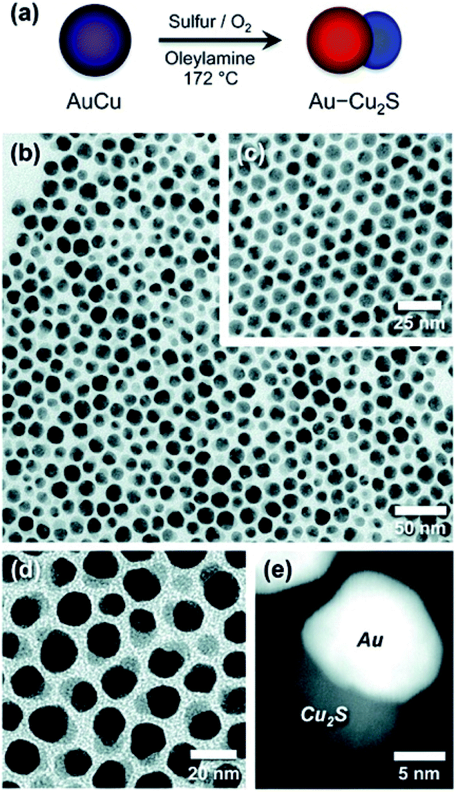 | ||
| Fig. 6 Chemically induced phase-segregation mechanism for the synthesis of Au–Cu2S heterodimers. In this mechanism the sulfidation does not partially convert the metal core—as depicted in approach (II) in Fig. 1—rather the bimetallic precursor phase-segregates into a dimer, with concurrent sulfidation of the copper into Cu2S, i.e., combination of approach (III) in Fig. 1 and sulfidation. (a) Synthetic path scheme, TEM of (b) dimers, (c) AuCu NPs before synthesis, (d) higher-magnification of dimers, and (e) dark-field image. Reproduced with permission from ref. 146, American Chemical Society, copyright 2012. | ||
Silver is especially popular as the metal transformed into Ag2S.147,148 Han and co-workers, for example, formed various M–Ag metallic heterodimers (where M = Pd, Au, Pt). In a subsequent step, in the presence of PVP (polyvinylpyrrolidone) and Na2S the silver was sulfidized, resulting in a M–SC heterodimer.147 This effect can also happen unintentionally, as in the case of Ag NWs, which are sulfidized under environmental conditions.149
Furthermore, addition of another reactive precursor containing a different element can also form a ternary sulfide as demonstrated by van Embden et al., who have used a ‘one-pot’ organic-phase synthesis (S coming from CS2, and DDT being the solvent) to form either core/shell or heterostructures of Ag/Ag8GeS6.150
A binary semiconductor can also be partially reduced to the metallic element it contains to form a SC/M interface. From the electronic structure point-of-view, even a reduction of few atoms due to charging (e.g., Cd0 in a cadmium chalcogenide) has significant influence as it forms a trap.151 On a larger scale, an ammonia electrosynthesis catalyst was prepared by reduction of iron oxyhydroxide to form a core–shell αFe–Fe3O4 hybrid by annealing under a reducing H2(g) environment.152 Another interesting related example is the formation of a bimetallic thin layer in a HNS: Peng and co-workers have shown that for Pt/Fe3O4 core/shell triangular nanoprisms, an interfacial iron–platinum layer is formed.153 This serves as an epitaxial layer, and is therefore important as a possible synthetic tool to allow formation of heterojunctions using partial reduction of the SC.
Such an approach was also used to form hybrid bimetallic CdNi decoration of CdS NRs: in the first step CdS NRs were partially chemically reduced by dispersing calcined NR powder in an aqueous NaBH4 solution; subsequently, a photodeposition procedure on CdS/Cd NRs was performed in an ethanolic solution of nickel chloride salt, resulting in CdNi decoration of CdS NRs.154 Aqueous-phase reduction using NaBH4 was used to form a complex Ag/AgBr/BiVO4 photocatalyst.155 First, AgBr was precipitated over hydrothermally prepared BiVO4 microspheres from a solution of Ag+(aq) and Br−(aq). Then, silver NPs were deposited over the AgBr domains by reduction of silver cations. In such a mechanism the solubility product of the AgBr determines the available concentration of silver for the reduction step, effectively transforming an AgBr NP into an Ag/AgBr dimer.155
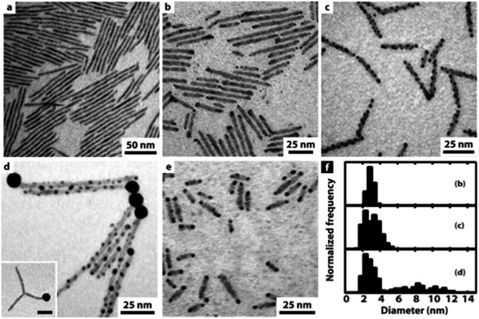
Reduction of Au(III) using DDA (a low AuCl3 concentration as the reactant source) in the presence of CdSe NWs and DDAB surfactant results in predominant growth at the tips (Fig. 7A). Increasing the Au/NW ratio results in enhanced overgrowth, probably on surface-defect sites. Further increase of concentration changes the mode of growth, with a transition from individual growth sites to areas of continuous overgrowth (Fig. 7C). At the highest concentrations, the integrity of the CdSe NW itself is endangered due to severe strain originating from the lattice mismatch of wurtzite (hexagonal) CdSe and cubic Au.165
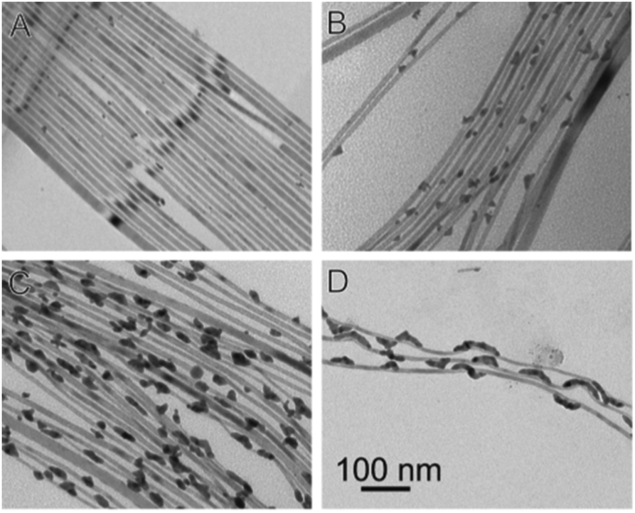 | ||
| Fig. 7 Gold overgrowth over SLS-grown CdSe NWs.165 Increasing amount of Au precursor from (A) to (D). Reproduced with permission from the American Chemical Society, copyright 2009. | ||
From the synthetic point of view, an important feature to achieve monodisperse size distribution of the CdSe NWs is the need for homogeneity of the Bi catalyst for the SLS mechanism. In the latter example, it was achieved by using a thin film of Bi deposited on a Si substrate, which melts and forms uniform droplets as had been reported by Wang and Xia.166
A recent study from the Waclawik group demonstrated a colloidal synthesis of different ZnO NC morphologies with a labile and relatively weakly bound ligand—benzyl amine. They have studied gold photodeposition on four different morphologies, in EtOH or EtOH:toluene mixture as the solvent (sometimes deaerated), with pulsed or continued irradiation.167 Photolysis of AuCl4− using UV illumination produces a metastable Au(I) complex [AuCl2]−, which in turn is reduced by excited electrons from the ZnO NC.63 They have shown that adjusting the described parameters allowed control over the average Au NP(s) per ZnO, as well as facet selectivity. They conclude that the most important factors are the charge distribution along the surface of the excited ZnO NC (influencing factors: shape, solvent and dissolved oxygen concentration, irradiation technique) and the energy barrier to nucleation at potential nucleation sites, which are determined mainly by the crystal facet and defects therein.167
Chen et al. have shown that by synthesis of ZnO nanoflowers using zinc stearate in a suspension of Ni@Au with OY, dibenzylether and hexadecanol they could form a hybrid that exhibits preferential orientation between the metal core (ca. 14 nm) and the ZnO pyramid (each ∼28 nm petal of the nanopyramid is a triangular pyramid).168 The Ni (111) plane is parallel to the wurtzite (0001) plane, which is a form of homoepitaxy, with most flat Ni facets acting as the nucleation and growth sites for the ZnO.
An important example for the thermodynamics of such systems was shown by the authors' group, where metal (Cu, Ag or Au)–ZnO nanopyramids with a selective metal attachment to the base or the tip of the pyramid were synthesized. In both cases, a one-pot reaction was carried out in the presence of oleic acid and oleylamine, which are the reducing and capping agents.169 When ZnO pyramids were present in the solution during the reduction of metal monomers, selective growth on the tip occurred (‘tip-attached’); when the precursors for both materials were heated-up, ‘base-attachment’ occurred since ZnO grew over the faster-forming metal NCs. This demonstrates the importance of the reactive sites. Once nanopyramids were present in the growth solution, the metal tended to nucleate on the vertex, due to the high surface energy of this geometry.58,72
As was described for these M/ZnO systems, there is a large mismatch between the lattice distances, which prevents formation of complete anisotropic core–shell systems. One way to circumvent this limitation is using a hydrothermally prepared coating of TiO2 over Ag NW cores, which allows deposition of multiple ZnO NPs as the sheath.170 Since Ag NWs have potential application as the main ingredient of conductive transparent (flexible) electrodes, such hybrids are of much interest, and simple deposition techniques (spin coating and mild thermal annealing) were used to this end to form ZnO NP/Ag NW composite mesh over polyethylene terephthalate (PET) as an example.171 Since the outcome is attachment based on random physical interactions without controlled interfaces, we will not discuss this synthetic approach further.
The previously discussed, Au-tipped Cd-chalcogenide system provides further insight into the formation of asymmetric hybrid structures from symmetric ones.72–74 Despite the symmetry of CdSe NRs in a colloidal solution, the gold complex is attracted to the tips. This stems from the combination of the following: (i) the tips are a location with a strong curvature, thus they have a high specific surface free energy (γ), relative to the sides of the NRs, (ii) the surfactant passivation at the tip is less ‘dense’, with higher defect probability both due to geometric considerations and the different exposed crystal plains (which during the high-temperature growth of the wurtzite hexagonal CdSe phase of the NRs grow parallel to the c-axis, i.e., 〈001〉). For these reasons, there is both a kinetic tendency for reduction on a tip (high number of Au-complexes adsorbed at the tip, and others with relatively easy access) and a thermodynamic one (γ). It is worth mentioning that removing part of the passivating NR ligands prevents the selective growth at the tips as in the report on the growth mechanism of Co on CdSe NRs by the Alivisatos group.79 Another consideration for single metal tip formation was demonstrated in a CoPt/CdS NR system. Here, unlike Pt under the same reaction conditions, Co does not nucleate on the CdS NR without an existing Pt tip, as its precursor is not reactive enough.78 In this mechanism, a Pt tip is formed (which could also be aided by the Pt–S interaction to the CdS at the tip) before a subsequent Co co-alloying occurs. In contrast to bimetallic alloy NP formation in solution, where each NP has a uniform Co and Pt distribution, in this case, a complete alloying of the Pt tip with Co takes place (fcc solid solution), but as the tip grows, strain release becomes possible by Co segregation or enrichment of Co at the later stages of tip growth.
The other point that needs explanation is why a low concentration of gold usually results in deposition on a single tip, forming an asymmetric structure. This is explained by the crystal structure of the NR that has one Cd-terminated end while the other end is chalcogenide-terminated. The electron-rich chalcogenide facet is expected to have higher reactivity towards gold reduction.74 The formation of asymmetric structures is not limited to the initial stages of metal deposition. With increasing concentration, after both ends of the NR are with Au tips (nano-dumbbell), a ripening process occurs, where small Au domains dissolve (due to both higher specific surface free energy and easier oxidation of small Au domains).172 This is an electrochemical ripening process that benefits further growth of the larger Au domain, since the free electron from the dissolving small domains migrates through the NR to the electron sink.
To achieve a metallic gold shell over CdSe dihexagonal pyramidal nanostructures, Meyns et al. have used wurtzite CdSe NCs as the seeds for a modified AuCl3 reduction procedure.80 They have reacted the NCs in the presence of OY and an Au(III) complex resembling Au(III)–DDAB (specifically, AuCl3 with n-dodecyltrimethylammonium bromide, DTAB). Under these reaction conditions, the OY surfactant is a mild reducing agent and a thin (partial) amorphous gold shell was formed around the CdSe NCs. When irradiated under a TEM electron beam, this shell transformed into Au dots on the vertices of the NC. This observation demonstrates several important lessons: (i) it shows the importance of high γ locations on a NC—when the reaction conditions allow a metastable state to reach the most thermodynamically stable one—high-energy vertices are classical nucleation points; (ii) crystal structure, morphology and ligand-passivation play a crucial role—when CdSe NRs of the same crystal structure are subjected to the same procedure, the result is the established double Au-tipped CdSe NRs. Since both morphologies have the same crystal structure, the empirical difference is attributed to (a) denser ligand coverage of the NRs, which poses a kinetic barrier to reduction on the NR's surface, thus the gold reduction occurs preferably on the tips (as discussed earlier); (b) despite sharing the same crystal structure with the NRs, the bipyramids have many Se- or Cd-terminated {101} surfaces, on which gold interacts with the Se (while the Lewis base moiety of the surfactant attaches to Cd atoms, which are Lewis acids). Additionally, a note of good practice is to remember that high-energy electron microscopy is not a ‘sterile’ environment and can induce not only beam damage but also chemical transformations, i.e., reduction (and in fact, using a stronger reducing agent, gold dots were formed on the vertices during the synthetic stage).80
In a subsequent report, Klinke, Juárez and co-workers tackled the oxidation state of gold not as a post-modification but during the synthesis itself.173 They have elegantly shown that using Au(I) or Au(III) complexes changes the final deposited gold morphology. They have switched the surfactant from alkylamine to dodecanethiol to easily obtain a solution of Au(I) precursor. Using the Au(III) complex only (with a subsequent addition of surfactant for stabilization), a shell was formed. When on the other hand, they injected an AuCl3–DTAB complex mixed with the DDT, i.e., an Au(I)-complex, the ‘standard’ gold dot nucleation occurred on several vertices of the CdSe NC.173 This report also explains the unstable gold shell as being composed of AuSe or AuSeCl (the Se source is the etching of the CdSe NC by the halide anions present).
For further discussion of the factors governing the formation of heterostructures vs. multi-component mixing, i.e., formation of solid solutions during synthesis, we refer the reader to a review by Jeong and co-workers.174
We have not explicitly discussed anionic and cationic exchange reactions177 of a semiconductor and galvanic exchange reactions of metals, but these are indirect synthetic paths to transform one domain of an HNS into another when the starting materials are more compatible and have a known proven syntheses. These reactions expand the possible attainable HNSs. For example, starting with a Pt–MnO heterodimer allows its transformation into Pt–MnE (E = S, Se), and finally to Pt–ME (M = Cu, Ag),178 or Zeng and co-worker's letter on Fe3O4/M mentioned in Section 2.1.2,108 where the aqueous-phase synthesis allowed further redox-based transformation of the metal (e.g., Ag into an AgPt alloy, Au into an Au@Pd core@shell).
2.2 Transition-metal–nonmetal compounds and other materials
In the previous section a description of interfacing different 2D semiconductor materials with a metal junction (for example, Ni/CdS nanosheets and Pt/CdSe NPL, shown in Fig. 2c and 4f, respectively, or Ni NP decorating MoS2 (ref. 179)) was given. Such materials have relevance to transistor (opto)electronics, hence various interfaces are formed via non-colloidal methods.180 The strong van der Waals (vdW) interactions between 2D layered materials such as graphene,181,182 phosphorene,183,184 transition metal dichalcogenides (TMDC),185,186 graphitic carbon nitride,187,188 and hexagonal boron nitride (h-BN)189 allow numerous opportunities to interface 2D–2D materials. The vdW interactions are a fascinating synthetic approach as it can direct the integration of mixed dimensionalities ranging from 0D to 3D complex structures into a variety of devices and architectures.180,190 In the colloidal synthetic realm, usually an exfoliation step is required before interfacing with metals,191 metal cations (which may transform the 2D substrate, see Fig. 8a–c)184 or other material classes. We refer the reader to a review by Dubertret and co-workers on 2D colloidal nanocrystals.192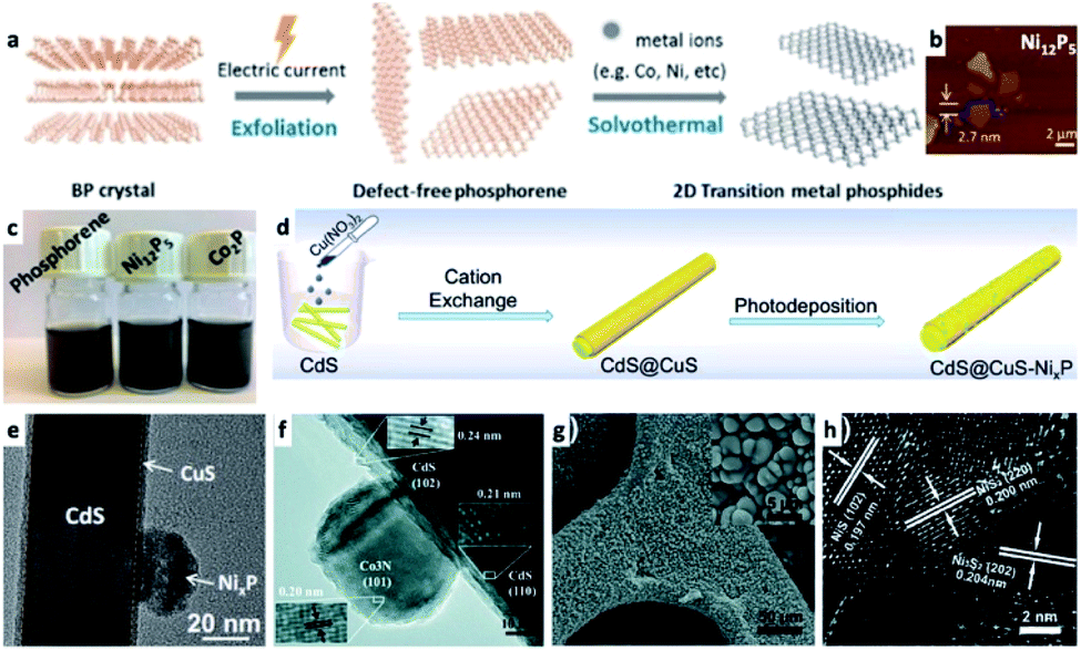 | ||
| Fig. 8 Examples of transition-metal (TM)–nonmetal compounds and their hybrids or chemical transformations. (a–c) Transformation of a 2D phosphorene into transition metal phosphides (TMPs) such as Ni12P5 and Co2P;184 (a) synthetic scheme showing that after an exfoliation step, a solvothermal reaction in the presence of TM ions forms the final product, (b) an atomic force microscope (AFM) characterization of Ni12P5, (c) images of vials with the dispersions. (d and e) A NixP TMP/CdS@CuS HNS; (d) a synthetic scheme where CdS NRs are coated with a CuS shell via cation exchange, followed by photodeposition of NixP, (e) TEM of this HNS, adapted from ref. 220 with permission from Elsevier, copyright 2019. (f) Co3N/CdS HNS formed by a hydrothermal reaction of cobalt nitrate and an amine source (hexamethylenetetramine) in the presence of CdS NRs, reproduced from ref. 207 with permission from the Royal Society of Chemistry, copyright 2017. (g and h) NixS/Ni HNS formed by sulfidation of a nickel foam substrate: (g) SEM, (h) HRTEM, reproduced from ref. 230 with permission from the Royal Society of Chemistry, copyright 2018. (a–c) Adapted from ref. 184 under a Creative Commons Attribution License, published by Wiley-VCH Verlag GmbH & Co., copyright 2020. | ||
Other classes of interfaces receiving tremendous attention in recent years mainly due to their promising catalytic abilities are metal-containing molecular species,193–196 hydrogenase enzymes,197 metal–organic frameworks (MOFs),198 and even metal-encapsulated MOFs.199–203 Since their attachment to the SC is usually chemisorption or some physical interaction (electrostatic), they are out of the scope of this review. Recently, Wolff et al. have demonstrated that molecular Ru-containing cocatalysts can augment classical CdS nanorod/Pt hybrid systems and achieve water splitting without sacrificial substances.204
An account from the Eisenberg group relates the development of Co and Ni containing molecules as alternatives for Pt or Pd as the catalysts for proton reduction to hydrogen.205 Simply put, after achieving the described significant progress in homogeneous catalysis using Co- and Ni-complexes, inspired by the dye-sensitization of semiconductors such as CdSe QDs, they have investigated the catalytic enhancement of aqueous dispersions of CdSe QDs using Ni2+ and Co2+. This account demonstrates how knowledge transfer between homogeneous molecular catalysis and heterogenous nanoscale catalysis is fruitful. Ni and Co as representative examples are now used not only as constituent atoms in molecular surface modifiers, but rather are part of a wide range of transition-metal (TM) based binary and ternary materials.
The transition metal chalcogenides (mostly oxides and sulfides) and pnictides (nitrides and phosphides) are common cocatalysts for photo- and electro-catalysis. Some of them have a metallic character, for example transition-metal phosphides (TMPs), which can be viewed as P-doped metals (Ni, Co, Fe, Mo, Mn, Cu),206 and TM-nitrides (e.g., Co3N, a metallic interstitial compound used in a Co3N/CdS NR HNS shown in Fig. 8f),207 while others can be semiconductors of varying bandgaps (e.g., Co3O4 (ref. 208) and late transition metal monoxides such as CoO,209 which have size-dependent band positions210). Generally, the catalytic activity of cobalt oxides stems from charge transport properties and the valency of the metals in the crystals, which is analogous to molecular systems. An important example is the use of CoO as a hole acceptor from a photoexcited TiO2 nanostructure, where a spatially separated Pt domain simultaneously acts as an electron acceptor.211 Other examples include a heterogeneous Ni–O bond containing cocatalysts on CdS (/Ni(OH)2,212 /NiO,213 /Ni2O3 (ref. 66)) and related systems,214–216 which resemble homogeneous molecular Ni-catalysts adsorbed on CdSe for hydrogen evolution.212
TMPs217 are common as the metallic cocatalysts in colloidal SC/M systems. Hybrid systems with a light absorbing semiconductor such as CdS include CdS QDs–TMP (CoP, Ni2P and Cu2P)218 and CdS NRs–TMP (MoP,219 NixP and CoxP220), which were used for water reduction, while electrostatically assembled Co3O4 on CdS NRs were used as water oxidation catalysts.221 It is important to stress that not all phosphides have metal-like properties, and various semiconductors are constantly synthesized and their properties are investigated, for example 1D SnIP.222
In the field of electrocatalysis various sulfides, phosphides, nitrides, oxides and (oxy)hydroxides are common catalysts, which are deposited on a substrate that serves as the electrode and they enhance either or both the activity and stability (for example, due to higher stability than the Si substrate in a strong alkaline environment).223–227 A common starting high-specific-surface-area metallic substrate is nickel foam (NF), on which gas-phase electrodeposition and a variety of solvothermal reactions are used to deposit the metallic catalyst. Various redox catalysts were deposited on NF such as binary Ni-based materials, e.g., Ni2P,228 Mo-doped Ni2P,229 ternary amorphous tungsten-doped NixP,228 or multiphase nickel sulfides,230 taking advantage of the abundant Ni surface. Electrodeposition allows forming CoPi over NiFe foam as well as Ni and Co oxides over NF.231
3D crystalline Co/amorphous Co3O4 core/shell nanosheets were demonstrated by a solution-phase deposition of cobalt oxide on the NF substrate, followed by partial reduction using hydrogen at 200 °C (where the newly formed Co crystals are the core of the amorphous Co3O4).232 More complex systems include NF supported 1D/1D hybrids of Ni12P5 nanowires over Ni3S2 nanorods233 and Pt over NF that was transformed into a mixture of nickel phosphides via solvothermal phosphorization.234
Phosphorization is also common in the gas-phase, for example by decomposition of NaH2PO2 at elevated temperature under a protective Ar atmosphere to transform a Ni/Cu/polymer into Ni2P–Cu2P@NiCuC,235 or trialkylphosphines over different metal foils, under 5% H2/Ar flow to eliminate surface oxides.236 In another recent phosphorization example, In-doped cobalt oxide was transformed into CoO/CoP for OER application in metal–air batteries.237 Another approach is formation of a hybrid structure which uses low amounts of precious metal (for example, Co2P/Pt core/shell NRs),238 and subsequently deposit it on an electrode, possibly in the form of a carbon matrix.
Recently, novel approaches have been utilized for the formation of 3D porous substrates via metallization, for the subsequent transformation into metal phosphides etc., for example using virus templates to form Ni3P or Ni2P and Ni5P4.239
This class of materials are treated in this review as semiconductors due to the similarity in the synthetic methods to other binary and ternary semiconductors as demonstrated in the work of Shavel and co-workers who have synthesized various colloidal TMPs of different aspect ratios.240
2.3 The HNS as a platform for hollow NPs
An interesting synthetic path to achieve hollow nanostructures has been demonstrated by several groups involving types of core@shell morphologies.241 Hollow NP formation is especially easy to detect when the formation is performed in situ using the electron beam of an electron microscope.242 Alongside the previously mentioned selective metal etching (using I2) of an HNS, leaving voids in the SC (Fig. 9a–c),130 one of the most common methods to achieve hollow NSs is the nanoscale Kirkendall effect,141 where a void is formed in NPs due to a significant difference in diffusion rates. In their report, Yin et al. have first demonstrated a designed experiment that harnesses this effect on the nanoscale with Co NPs. They showed how cobalt is sulfidized upon addition of a sulfur solution into a pre-heated Co NP solution. The hollow Co9S8 (at different Co/S ratios, also Co3S4 or their mixtures) is formed because the Co core that leaches out through the CoS shell much faster than sulfur is able to diffuse from the exterior, through the formed shell, resulting in hollow CoS as a representative cobalt chalcogenide. Another example is the formation of Ag2S nanotubes from ZnS NRs while the metallic Au tip is transformed into a bimetallic AuAg tip (Fig. 9d–h).243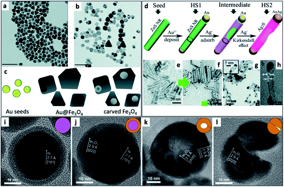 | ||
| Fig. 9 Hollow nanostructures derived from HNSs. (a–c) Au NPs serve as seeds for the growth of a shell (Au@Fe3O4, TEM shown in (a)), subsequently etched with iodine, removing the gold and resulting in carved Fe3O4 (b); scale bars are 100 nm; (c) scheme.130 (d–h) The nanoscale Kirkendall effect is responsible for the formation of Ag2S nanotubes with a gold–silver tip: (d) the synthetic scheme, (e) ZnS NRs (d ∼ 3 nm) serve as seeds for the reduction of gold on its tips (HS1, shown in (f)); following the exposure of HS1 to Ag+ ions two phenomena occur—the Au tip is alloyed to form an AuAg tip and the rod is transformed via the Kirkendall effect (silver cations diffuse inside, replacing the zinc cations, which diffuse outside) resulting in a hollow silver sulfide nanotube, Ag2S NT/AuAg (HS2); confirmation of the mechanism is evident from TEM images (g), where d ∼ 5 nm; a wall thickness of 0.8 ± 0.1 nm is confirmed by (h) HRTEM.243 (i–l) Hollow indium oxide NPs are formed via a non-Kirkendall mechanism in a deaerated atmosphere,249 namely In NPs (i) with a native amorphous InOx shell are first thermally oxidized to form an In@In2O3 core@shell (j), additional heating is responsible for crack formation due to thermal expansion and void-formation, resulting in hollow In2O3 (k); some NPs exhibit significant cracking shown in (l); the inset of every TEM image contains a schematic cartoon of the NS. (a–c) Adapted from ref. 130 with permission from the Royal Society of Chemistry, copyright 2018. (d–h) Adapted from ref. 243 with permission from the Royal Society of Chemistry, copyright 2015. (i–l) Adapted with permission from Wiley-VCH Verlag GmbH & Co., copyright 2013. | ||
A ‘reversed’ nanoscale Kirkendall effect has also been reported, where Au-decorated an InAs HNS was used as the starting material for the formation of a crystalline metallic Au core/amorphous (oxidized) InAs shell with voids due to faster inward diffusion of Au in an InAs matrix compared to the self-diffusion of InAs (outward).244 An additional limiting case of a Kirkendall effect was exploited by Manna and co-workers, who have used the different susceptibility towards oxidation of the ingredients of a copper selenide core/copper sulfide shell nanocrystals.245 They showed how Cu+ ions diffuse into the solution upon exposure to an oxidizing etchant (CuCl2). Subsequently, Cu+ cations diffused outwards from the Cu2−xSe core through the Cu2−xS shell, thus forming various hollow particles, including collapsed NCs. Though not a regular M/SC HNS example, it shows how similar systems can be used to expand the scope of synthesized multicomponent nanostructures (e.g., via cation exchange,246,247 and confined nano-to-micro particles).241,248
A related anion exchange phenomenon was exploited to form (hollow or void-containing) ZnS@Sn:ZnO nanostructures.250 Furthermore, different diffusion rates can be used to transform hybrid CdSe/Cu3P nanoplatelet systems into Cu2Se.251 Combination of such exchange strategies alongside selective etching was reported by Fenton et al. who formed various multi-domain nanostructures with combination of metal-sulfides, metals and voids.252
Another non-Kirkendall effect has been demonstrated using In@In2O3 core@shell NPs, which fractured upon heating to 250 °C due to the melting of the low-melting-point metal core. As a consequence, hollow indium oxide NPs were obtained (Fig. 9i–l).249
3 Formation of complex nanoparticle systems
3.1 Rational design of nanoparticles with increasing complexity
Multicomponent nanoparticles can be synthesized with multiple materials and domains, thus benefiting from two or more interfaces, at least one containing an M/SC junction. The final morphology can be a variant of a core@(multi-)shell, different multi-domain nanostructures and combinations thereof. Fig. 10a is a schematic representation of various multiple-heterojunction morphologies, which are attained from a single nanoparticle, starting with an ‘A’ NP, which can react with ‘B’ and consequently with ‘C’.253 In Fig. 10, some possible heterotrimer morphologies are depicted resulting from deposition of material ‘C’ on ‘A–B’ dimers that were formed in a previous step, adapted from Hodges et al.253 The Schaak group has thoroughly investigated the depicted heterostructures,253–256 and has even expanded the breadth of these methods, for example, by introduction of a solid-state protective group. Without a protective group (from A–B to C–A–B, marked with a green arrow in Fig. 10a), the third material (the metal) is formed on the metal of the dimer (TEM images in Fig. 10c and d show deposition of Au on Pt–Fe3O4 dimers, forming an Au–Pt–Fe3O4 heterotrimer).254 If, on the other hand, the dimer involves a thin shell, as is the case in the Pt@Fe3O4 example shown in Fig. 10e, where Pt is completely coated with Fe3O4, the subsequent Ag deposition occurs on the iron oxide, opposite to the Pt domain (without the protective group an Ag–Pt–Fe3O4 formed).256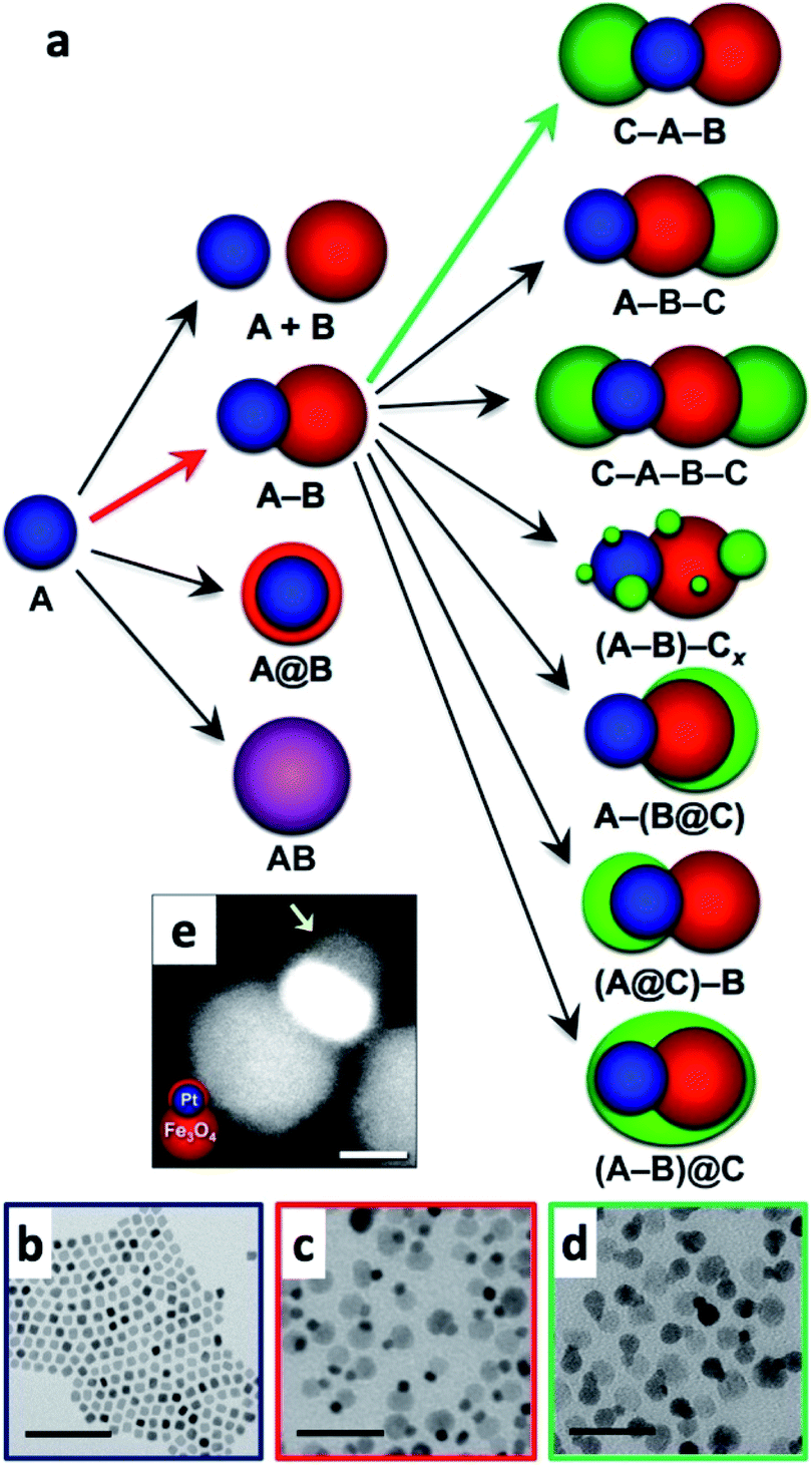 | ||
| Fig. 10 Sequential seeded-growth allows formation of various higher-order hybrid nanostructures, namely heterodimers and heterotrimers. (a) The first reacting NP is A (blue), which reacts with a second B NP (red), which in turn results in either a mixture of A + B, a heterodimer (A–B), a core@shell morphology (A@B) or an alloy particle (AB in purple implying a solid solution has been formed). The A–B heterodimer serves as the seed for deposition of a subsequent third material C (green).253 (b–d) TEM examples of the process depicted in (a) using color arrows: (b) Pt cubes serve as the seeds for formation of (c) Pt–Fe3O4 heterodimers (through the red arrow) that in the final step (through the green arrow) serve as seeds for selective gold deposition on the metal domain, forming the (d) Au–Pt–Fe3O4 heterotrimer.254 (e) Variation of A–B formation, where Fe3O4 forms a thin shell over the Pt in this heterodimer example with a protective layer.256 Adapted with permission from the American Chemical Society, (a–d) copyright 2017, (e) copyright 2014. | ||
An example of a core–multi-shell HNS is Au NRs, which are transformed into Au/AuAg to utilize the option of sulfidation, allowing the synthesis of Au/AuAg/Ag2S by reacting with thioacetamide in a basic environment. Finally, an additional shell layer of PbS could also be synthesized.257 A synthesis in the organic phase can also be used to form multi-shells as demonstrated by our group for M@ZnS@ZnSe (M = Ag, Au).258
Amongst the multi-domain HNSs, a system that was discussed previously and was explored in our group is the single-tipped semiconductor nanorods, where the metallic tip acts as an electron sink, thus serving as an excellent reduction catalyst (further discussion in Section 4.2). As SC NRs with a single metal tip have beneficial photocatalytic properties, and we had already shown that it is possible to deposit metal-sulfides selectively (e.g., PbS, Ag2S and Cu2−xS) on a tip of Cd-chalcogenide NRs,259 we combined these two kinds of interfaces into a single multi-component NR, which is based on a CdS (or CdSe-seeded CdS, i.e., CdSe@CdS) NR with two distinct domains on opposite tips: PbS and Pt, forming a SC–SC–M system (PbS–CdS–Pt).90 The rationale behind this system is to enhance the charge-carriers’ lifetimes by suppressing recombination due to spatial dissociation, i.e., the electrons are preferably located at the metal tip, while the holes (h+) reside on the other end of the complex heterostructure, since PbS acts as a h+ sink.
Transient absorption measurements confirm the described kinetic model, but unfortunately, the photocatalytic activity of the PbS–CdS–Pt system does not significantly improve relative to the CdS–Pt one, probably due to the combination of the following: (i) the systems' relatively flat conduction band does not provide sufficient thermodynamic driving force to transfer the electron from the CdS into the Pt tip, while the hole is tightly bound in the PbS, and (ii) electrons are being trapped at the PbS–CdS interface.90
Since it is a synthetic challenge to deposit two distinct (single) domains on each NS, Alivisatos and co-workers used a modified approach: they have synthesized a CdSe–Ru dimer as the seed for CdS NR growth. The CdS was successfully grown from the CdSe seed, which resulted in a CdSe@CdS NR with a Ru domain on the surface of the NR (the alkyl chain-length of the employed phosphonic acid could influence the seed position in the CdS). As a final step, a Pt tip was deposited on the NR, resulting in a Ru/CdSe@CdS/Pt HNS.260
Schick et al. have adapted an encapsulation procedure of MnO in silica to selectively encapsulate only the MnO domain of an Au–MnO heterodimer using a reverse microemulsion technique.261 This can be considered a multi-domain formation (a heterodimer) followed by a core–shell formation. The advantage of this method is that the encapsulation does not work on the metallic domain, and leaves it free for further functionalization with thiol molecules, which can allow dispersibility control and facilitate possible biocompatibility-requiring applications such as targeted drug delivery or imaging techniques taking advantage of the simultaneous optical and magnetic responses.261
Mirkin and co-workers have published a detailed analysis of palladium–tin alloys showing the possible multiple-domain HNSs with several metals (Ag, Au, Co, Cu) and their bimetallic versions and how they could be spatially arranged up to tetraphase nanoparticles containing six elements.262
Significant progress has been achieved by the Schaak group which has used heterodimers (as shown in Fig. 10) as the precursors for development of a wide array of complex inorganic nanostructures with a consecutive-step chemical approach (‘total-synthesis framework’).51,253,254 A Pt NP can serve as a nucleation site for Fe3O4via thermal decomposition of Fe(CO)5 in the presence of Pt seeds, for example, forming a Pt–Fe3O4 heterodimer. Then, another metal NP can be selectively placed on the Pt at an opposite direction to the Fe3O4 domain, resulting in an M–Pt–Fe3O4 (M = Au, Ag, Ni, Pd) structure.50 The chemical selectivity is interesting as the M does not nucleate on the iron oxide, nor at the Pt–Fe3O4 interface. This selectivity is explained by electron-transfer to the Pt domain, which then facilitates the reduction of the M domain on its surface. A third interface was also added to this system, forming a linear chain of four components, that is an MxS–Au–Pt–Fe3O4 heterotetramer, with selective formation of a metal-sulfide (in this report Cu2−xS and PbS) on the terminal gold.50 The key factor to the reported selectivity of the metal-sulfide to the gold is a kinetic competition between reaction of the Cu(I) precursor with the S and the adsorption of S to the HNS. Since sulfur is adsorbed faster on the gold, this is the site where it further reacts to form the metal-sulfide.50 A variation of this approach was used by the same group to grow several metal-nitrides on noble-metal seeds; specifically, a three component system was investigated: Cu3PdN nucleating on Pt nanocubes–Fe3O4 dimers.263 In this case, the nitride formed preferentially on the corners of the cubic Pt domain while using spherical seeds of Au or Pt results in a core@shell structure. Shi et al. have shown already in 2006 that using nucleation of a semiconductor PbE (E = S, Se) on a metal can be used to form a ternary hybrid Fe3O4–Au–PbE.264 The lead chalcogenide nucleates on the available gold domain, which under certain conditions resulted in the formation of PbS NRs as the third component.
The previously described approach is based on successive nucleation events. An alternative mechanism was also reported by Schaak and co-workers, who have used supersaturation and precipitation to transform heterodimers into heterotrimers (in this case, Au–Fe3O4 into Au–Ge–Fe3O4).265 In this pathway, the metal domain of a heterodimer acts as the center of precipitation for a third material, once it has been supersaturated. This method is less versatile than the ‘regular’ heterogeneous nucleation but has the benefit of minimizing the limitations of surface phenomena and allows the insertion of a distinct metal domain between the metal catalyst and its semiconductor partner in the parent dimer.
Our group has successfully used a related approach to insert a metal-sulfide semiconductor (i.e., CdS) between a preformed ZnO NR–Au tip. As shown in Fig. 11, the CdS precipitates out of the metallic Au–Cd core, pushing the ZnO NR during the synthesis.266 We proposed that this insertion mechanism is a form of an SLS growth as the gold tip is alloyed with Cd at the reaction temperature (320 °C), and it serves as the catalyst for CdS precipitation.
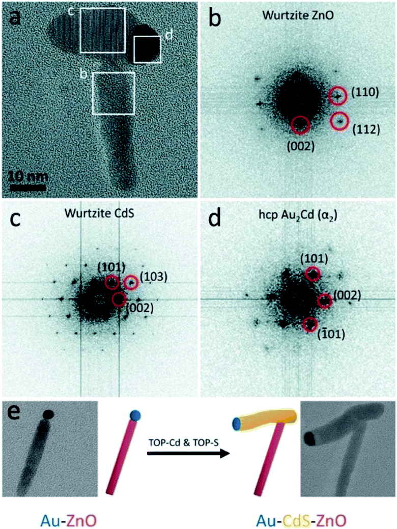 | ||
| Fig. 11 Ternary hybrid system using an SLS mechanism. (a) High-resolution TEM image of Au–CdS–ZnO with marked areas for fast-Fourier transform (FFT) analysis: (b) from the ZnO, (c) from the CdS, (d) from the Au–Cd. (e) Synthetic scheme and TEM images: Au–ZnO NR formed using the seeded growth approach is reacted with Cd- and S-complexes to insert a CdS domain. Reproduced from ref. 266 with permission from the Royal Society of Chemistry, copyright 2017. | ||
An additional option to obtain a complex heterojunction-containing colloidal structure is attachment of different structures in the system as discussed in the review by Buck and Schaak,51 followed by fusion. This is usually achieved by controlled elimination of stabilizing agents, which favors controlled aggregation, for example using iodine to ‘weld’ different Au-(multiple) tipped nanostructures as reported by Manna and co-workers.267
The ability to form three-component systems can also be used as an intermediate synthetic pathway to achieve two-component products, where the third component acts as a protective layer—to be removed during synthesis. This was reported using a polymer by Xia and co-workers for formation of bimetallic Au–M (M = Ag, Pd, Pt) NPs,268 and also in an all-inorganic system by Chen and co-workers, where a silica is protecting a gold core, i.e., an Au–SiO2 dumbbell is reacted with another metal, which cannot conformally coat the Au-core due to the existence of the SiO2 mask.269
This allowed formation of Pd–Au and Pt–Au dimers, as well as Pt–Pd–Au trimers, where dendritic Pt domains were deposited on the Pd, before removal of the protective silica layer from the terminal gold NP. Silica is popular as a hard template that can be removed, as demonstrated in the formation of Pt–Fe3O4 HNS encapsulated in N-doped carbon hollow spheres by embedding the dumbbell in silica and polydopamine, which after carbonization and silica removal resulted in a yolk–shell morphology.270 Naya et al. have used ZnO, which dissolves under mild conditions to form a ‘nanoegg’ shape, of half-cut Au(core)–CdS(shell).271
3.2 Complex (higher-order) systems
In addition to increasing the complexity (e.g., morphology, number of components and functionalities) of a single colloidal nanostructure, the different domains constituting an ensemble of HNSs can be used to form complex high order systems such as 3D superlattices and other arrangements on substrates. Much progress has been achieved in using self-assembly for these purposes. For example, Chen and co-workers could successfully demonstrate it using pressure-induced interparticle fusion272 and more recently39 using patchy Au QDs coupled to interparticle distance control via variation of the passivating ligand shell to self-assemble them into different superlattices using NPs without an inherent anisotropy (Fig. 12). The same group also reported how patchy gold domains on CdS–Au2S Janus NPs migrate and coalesce to form CdS–AuS–Au heterotrimers upon pressure-treatment.273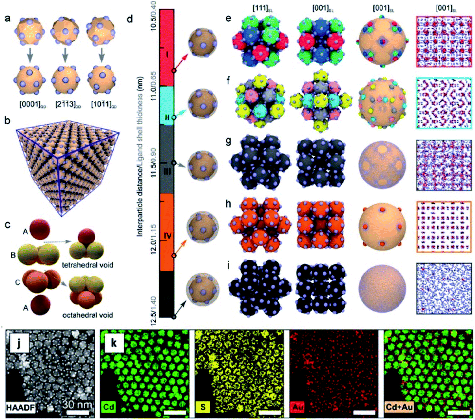 | ||
| Fig. 12 Self-assembly into superlattices from patchy quantum dot–gold hetero-structural nanocrystals without inherent anisotropy. The top part shows simulation of gold NPs on different facets of wurtzite QD hosts with varying interparticle distance adjusted by the ligand shell (surfactant chain-length) and the resulting unit cells: (a) satellite configurations of polyhedral and spherical models, (b) packing into a superlattice with a face-centered cubic (fcc) arrangement of individual patchy NCs, (c) illustration of the voids formed within the fcc lattice, (d) illustration of the five different orientational orders observed in the MD simulation, where the semitransparent gray highlight presents the length of the passivating ligand shell, (e–i) the different orientational order of the structures presenting different projections and a snapshot (right column) highlighting the contacts in red. The bottom part shows experimental high-angle annular dark-field scanning TEM (HAADF STEM) image (j) and the corresponding EDS elemental mapping of CdS polyhedra (9.7 ± 0.5 nm)/Au-satellites (2.2 ± 0.3 nm) HNSs after self-assembly (k), where Cd, S and Au are presented in green, yellow and red, respectively, and the rightmost frame shows the overlay of Cd and Au. Adapted from ref. 39 with permission from the American Chemical Society, copyright 2019. | ||
Integration into 2D predetermined patterns can also be achieved using the attraction of metal domains of the HNS to metal anchor points on a substrate (Fig. 13). Such integration was exemplified with Au/CdS NRs/Au nano-dumbbells forming ‘nanolithographic docking’ using the chemical affinity of dithiol molecules to AuPd nanodots on a Si substrate and the Au domains of the HNS.274
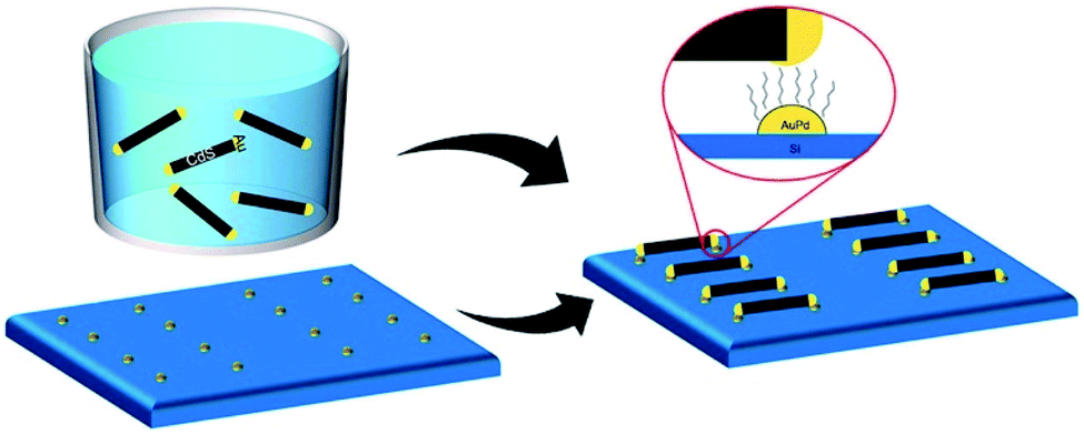 | ||
| Fig. 13 CdS–Au nano-dumbbells self-assemble on pre-fabricated AuPd NPs on a Si substrate (‘nanolithographic docking’).274 Reproduced with permission from the American Chemical Society, copyright 2018. | ||
4. Properties and applications
To utilize the unique properties of HNSs in many applications they must be connected to an external circuit when the electric response is required either as an input or an output, including sensing, photovoltaics, (photo)electrocatalysis and so forth. Since an electric signal is transported via metallic connectors, there are three common approaches to connect an HNS to an external electrode: (i) direct synthesis of the SC part on a metallic substrate as was discussed with the nickel foam examples in Section 2.2; (ii) deposition of a metal over a SC structure—a possible configuration for photovoltaic devices, where an active layer of semiconductor(s) is sandwiched between a transparent conductive oxide and metal electrodes;275 (iii) using the metal part of the HNS itself to serve as the anchoring point to an external macroscale measuring system, for example by connecting a metal to a nanoscale p–n junction. To achieve the latter, lithographic techniques as demonstrated in a recent report by Duan and co-workers186 are most common. As these three approaches are less suitable for colloidal HNSs they are mostly outside the scope of this review. Instead, we focus in this section on the utilization of the phenomena arising from the formation of colloidal HNSs in dispersion for (photo)catalytic, photoelectronic and some biomedical applications. Of note is that the solid-state Photovoltaic devices section (Section 4.3) deals with deposited HNS dispersions, which constitute the photoactive layer itself.For practical utilization of HNSs, the source of the favorable novel properties must be identified. Coupling a metal to a semiconductor can be beneficial for catalysis (Section 4.1) and can improve the light absorption through a plasmonic mechanism or improve the generated charge-carrier dissociation kinetics from the semiconductor—both mechanisms are elaborated in the photocatalysis subsection (Section 4.2).
The formation of a M/SC interface in a colloidal HNS solution also increases the conductance of individual NPs, as exemplified for CdSe NR/Au.276 Such phenomena can be used for characterization of multicomponent SC nanostructures using variants of probe microscopy277 on the one hand, and for providing a high-chemical yield method to connect metallic domain(s) on various NPs for further integration276 on the other hand. The latter is an alternative to the more traditional metal deposition through nanolithography, for integration into nanoelectronics as was demonstrated by the Alivisatos group.278 The exact mechanism of conductance enhancement in HNSs is still not fully understood and may change from system to system. Possible contributions (sometimes parallel) may stem from a lower Schottky barrier (shown in single NP measurements276 and CdSe/Au nano-dumbbells, which form linked networks),279 percolation of metallic domains, and different M–SC electronic coupling phenomena (including photoconduction in Pt–CdSe monolayers280) as discussed by Mahler et al., who conclude that the most likely explanation in the case of CdSe NPLs/Au is tunneling events between metal tips with little contribution (if any) from electronic states of the SC.70
4.1 Catalysis
An interesting example of interface engineering has been recently shown by Zhu et al., who have used galvanic replacement to partially exchange Cu NPs into Cu@Ag NPs alongside partial oxidation of the Cu to Cu2O.140 Control over the oxidation allowed formation of a thin layer (3–6 atomic layers) of Cu2O, which induced compressive strain at the NPs' surface, which was demonstrated as beneficial for the catalytic transformation of aniline into azobenzene (oxidation). Another common model reaction to test SC/M systems is the (photo)reduction of 4-nitrophenol (4-NP) to 4-aminophenol in the presence of sodium borohydride (NaBH4),117 which was recently shown to take place on the catalyst's surface—adsorbed 4-NP molecules are reduced using electrons from the catalyst and protons coming from the protic solvent (water, alcohol, etc. but not directly from BH4−).281The oxygen reduction reaction (ORR) is a reaction in the field of batteries (Li–O2 batteries, for example)282 and fuel cells,283 where an electrocatalyst (most commonly a precious metal) is responsible for the transformation of O2 into H2O (in the case of Pt(100) the ORR is performed via the oxygen dissociation mechanism).284 Using the interaction between the metal-oxide support and the metal,285–288 the energetics of the catalyst can be improved. Meng et al. have epitaxially grown Pt on single-crystal CuO NRs for this purpose.285 They have loaded a carbon cloth with fcc CoO NRs with pyramidal facets, which served as the nucleation centers for epitaxially grown fcc Pt NPs (∼7% lattice mismatch) using magnetron sputtering followed by annealing to achieve crystallization.
The reported Pt/CoO configuration results in electron donation from the oxide to the metal, which tunes the d-band structure of Pt in the hybrid system downwards, and results in favorable intermediate adsorption.289 This is an elegant demonstration of the electronic charge transfer into a metallic catalyst, which improves its catalytic efficiency. As pointed out by Wang et al., this is only one contribution to ORR activity and other effects such as particle size, crystal facets and lattice strain have a critical impact, which is usually hard to decouple from the charge transfer effect in hybrid structures (either M–support or M–M).289 Further advancement is expected when the metal-oxide support is doped, which can improve its conductivity, stability of the active electrochemical and specific surface areas, as well as tuning of the energy alignment with the metal catalyst.283
The hydrogen evolution reaction (HER) and related reactions are very common using a metallic catalyst coupled to a transition-metal chalcogenide or pnictide as was discussed in Section 2.2.290 As a rule-of-thumb, the most robust systems are expected to be grown directly on a conductive substrate that acts as the electrode, for example, Co/Co3O4 core/shell 3D structure over NF.232
Another electrocatalytic reaction of interest is the electrooxidation of alcohols. This reaction is usually performed using metal catalysts such as Pd or Pt and supported on metal oxides such as CeO2,104,291 TiO2,291,292 SnO2,291 Ni(OH)2 (ref. 293) and MoOx294 in alkaline media with a strong influence of the support on the selectivity of the process.291 The support–metal interaction is just another example of the novel properties arising in HNSs, which include charge transfer from the metal and improved oxygen binding of surface metal centers in the metal-oxide (surface oxygen vacancies); in electrooxidation these bound oxygen-containing species can be especially beneficial for the removal of poisoning intermediates from the metal surface.104 Other variants include PtAu/Bi2O3,295 Pt/CeO2/PANI (the polyaniline (PANI) polymer allowing 1D nanotube morphology)296 and Pd coupled to Co-doped CeO2 dots, which result in increased poisoning resistance.297 TMPs are also frequently used in conjunction with a carbon support, e.g., Pt over Co2P,298 PtP over NiCo2Px,299 and Pd/CoP.300 As a model electrocatalytic system, our group demonstrated EtOH oxidation using an insulating 3D scaffold of CaCO3 from a marine origin (Sorites), coated with cobalt and gold.301
4.2 Photocatalysis
Photocatalysis is probably the most common application of M/SC HNSs. The first step in a photocatalytic reaction is optical absorption, which is a light–matter interaction heavily influenced by the coupling extent between quantum states of the HNS's components. There is a strong influence of the material and shape of the SC (see for example, Kuno and co-workers),302,303 and it may be further altered after the formation of the M–SC heterojunction(s).As discussed by Sönnichsen and co-workers, CdS–Au matchsticks retain similar optical properties, while CdSe–Au dumbbells exhibit significant changes relative to their pristine SC NC.304 The strong M–SC interaction alongside spectral overlap between the CdSe excitonic band edge and the plasmonic Au resonance frequency leads to smearing of the ‘plasmonic’ absorption peak and complicates theoretical calculations. This observation leads the discussion to the second step in photocatalysis—generation of charge carriers and their migration. The basic model is that a semiconductor absorbs at its band edge (i.e., hν ≥ Eg), which leads to an electron excitation from the valence band (VB) to the conduction band (CB), where a hole is thus formed; a metal has a plasma frequency, where it also absorbs light, which if intense enough at the relevant wavelength causes excitation of free electrons, which in turn can participate in some kind of energy transfer.
Pradhan and co-workers have shown how the incorporation of Sb ions into a bismuth sulfide NR matrix improves light absorption of this non-heavy metal SC. These NRs were grown on gold seeds, forming a photocatalytically active Au–Bi2−xSbxS3 hybrid system.305 Two important features of this work are the shortening of the elongated Bi2S3 upon introduction of Sb with a single encapsulated Au NP per NR, and the addition of LSPR to the SC. It is important to mention that metal-sulfides are known for their strong localized surface plasmon resonance phenomena (due to sulfur vacancies). The energy of the resonance can be tuned by variation of the material as demonstrated by Gabka et al., who have synthesized Cu–Fe–S nanocrystals,306 or by formation of a heterostructure (variable ZnS domain length) to tune the nanoantenna (Cu1.96S) as was shown by Wang and co-workers.307 These materials allow a rational planning of hybrid materials, where the plasmonic response comes from the SC and not from the metal.
The third photocatalytic step is the charge and energy transfer phenomena, usually to the interfaces—the solid heterojunctions and to the surfaces of the HNS, where they meet the molecules relevant to the last catalytic reaction (surface bound ligands, solvent molecules and any other adsorbed molecule, including reactants). At this stage, the quality of the interface, the materials, and their morphology play a significant role (e.g., affecting the kinetics of electron transfer), as will be discussed for the relevant applications. For example, Yu et al. have shown a difference between electrons excited to the band edge (‘cold electrons’) and high-energy electrons (‘hot electrons’) in CdSe NRs. Comparing CdSe NR/Au and CdSe NR/Pt HNSs showed that hot electron (e−) injection is faster for the Au-tipped HNS while the cold e− injection yield is higher in the Pt-tipped one.308
To describe the role of the M/SC interfaces we deal with two main cases: (i) the metal serves as an antenna for light-harvesting through a plasmonic mechanism, and this energy can be transferred to the SC, thus enhancing the photocatalytic activity;125 (ii) the semiconductor absorbs the incident radiation, and the metal acts as a sink for the electrons, which can then perform a reduction reaction, while the holes remaining in the SC can perform an oxidation reaction. As in all heterogeneous catalytic reactions, the metal surface also provides adsorption sites.
The plasmonic mechanism is very appealing since this mechanism results in an experimentally improved absorption cross-section of the metallic domain relative to the purely geometric one309 (which is relatively low for small colloidal NPs). The metal can thus photo-enhance catalytic reactions,310 with an adjacent wide bandgap SC or insulator (a stable oxide) acting as a support. For example, the Linic group has shown the photocatalytic activity of alumina-supported silver nanostructures towards oxidation reactions.311 They have ascribed the plasmonic effect manifestation in the form of an electron transfer to antibonding orbitals of oxygen in the adsorbed reactants. Many others have used a variety of metal–metal-oxide combinations; some recent examples include Ag312 or Rh313 nanocubes supported on α-Al2O3, different Au NPs supported or coated on TiO2,314,315 SiO2,316,317 or both (i.e., Au@SiO2@TiO2),318 as well as multi-metal combinations as Al antenna–Ir NPs on an Al2O3 support319 for photocatalysis or for studying the interaction arising at the M/SC interface.320
Of note are the studies of Li, Wei and co-workers, who used plasmon-enhanced Au core(s)@MoS2 sphere shell HNSs for photocatalytic hydrogen production with stable high rates.321,322 In one configuration, the proximity between gold multimers (spacing of 5–10 nm) allowed enhancement of the absorption cross-section and an additional absorption frequency at ca. 630 nm appeared due to in-phase coupling in a single-material gold multimer system. A subsequent MoS2 shell formation results in an HNS with strong absorption both at the characteristic Au response (∼640 nm) and at the MoS2Eg (∼510 nm). The multimer hybrid thus exhibits both an improved absorption in the visible range and a higher energy transfer rate relative to single Au@MoS2, improving photocatalytic H2 production. The relative high stability of this colloidal system stems from the strength of the Au–S bond in the anchoring of MoS2 to gold and provides an additional photocatalytic advantage.321 The other system with high stability is the ternary HNS formed by reacting Au@MoS2 hydrothermally with a zinc source and an amine to form Au@MoS2–ZnO.322 The latter system benefits from the mechanical strength of the NRs in the composite (about 6–10 rods per sphere) and higher specific surface area, but more importantly, the introduction of ZnO alters the electronic structure resulting in improved light harvesting in the 350–700 nm range: a new absorbance intensity is measured in the UV (350–400 nm) and the authors ascribe the red shift of the typical MoS2 absorption at ca. 600 nm to 650 nm to the surface plasmon local field effect. Furthermore, ZnO, a known electron conductor, facilitates spatial charge separation, and in part is responsible for the reduced photocorrosion.322 For further plasmon-enhanced applications we refer the reader to a review from the Wei group regarding various metal–2D hybrids (graphene, MX2, BN, etc.).191
To explain the photocatalytic enhancement of the HNS, the commonly suggested modes of energy transfer are as follows: (i) the metallic NP, which absorbs the radiation performs a direct energy transfer between the LSPR and the coupled electronic state of a damping surface-attached chemical species (i.e., catalysis on the metal's surface), or (ii) indirect energy transfer, where the ‘hot’ carrier from the plasmonic structure is an intermediate agent that allows the dephasing of the surface plasmon and transfers the excess energy either as an electric charge or as vibrational energy to the interface at the surface.323Fig. 14 further elaborates the possible energy transfer mechanisms from the metal to the SC, based on the work of Cushing et al. on a silica-passivated M@SC shell (Au@SiO2@Cu2O).125 As they point out, there is still no consensus regarding which mechanism is at play for the reported systems, and novel probing techniques are constantly recruited for this task.324–327
 | ||
| Fig. 14 Various possible energy-transfer and separation processes responsible for plasmon-enhanced photocatalytic activity of Cu2O/Au-based HNS.125 (a) Scheme of energy absorption at the metal (pump) and the subsequent energy-transfer processes: (b–d) illustration of the metal core (Au) and the SC shell (Cu2O) energy positions (right) and processes (left): (b) direct energy transfer (DET), where LSPR ‘hot’ electrons are transferred to the SC's CB; (c) local electromagnetic field enhancement (LEMF), where the e−–h+ charge-separation in the SC is radiatively aided by the metal excitation; (d) resonant energy transfer (RET), where the LSPR dipole induces e−–h+ pair separation in the SC via a non-radiative mechanism that relaxes the localized surface plasmon dipole. Adapted with permission from the American Chemical Society, copyright 2012. | ||
One of the consequences of the plasmonic response is local heat generation through electron–phonon scattering,318 which has made a distinct contribution to successful photocatalytic CO2 methanation of Rh/TiO2, for example.318 It has been suggested recently that the catalytic activity of the generated ‘hot-electrons’, i.e., non-thermal charge carriers in the metallic nanoparticles (which are responsible for the photocatalytic enhancement reported for Cu–Ru NPs328 and others312,315,317) disregards the local heating effect of the plasmonic structures, and that the measured enhanced photocatalytic effects should be ascribed, in lieu, to thermal effects (well-described using a simple Arrhenius model).329–332
This intriguing explanation requires significant improvement of experimental apparatus and procedures both to perform correct control experiments and to allow the measurement of real local temperatures. It paves the way to further improvements by taking into account the resulting thermal gradients333 as well as rational design of HNSs that can sustain enhanced heat generation, for example by improving the heat conductance of the supporting oxide.330
The metal as an electron sink is the other common way to imbue enhanced photocatalytic properties to an absorbing SC nanostructure. The two most commonly reported photocatalytic applications are: (i) light-induced heterogeneous catalysis, mostly performed in a solution, where the colloidal HNSs are suspended, and (ii) photoelectrochemical cell (PEC) setups, where the HNSs are deposited on a photoanode or a photocathode. Colloidal-phase photocatalytic reactions are mainly oxidation or reduction reactions (possibly with radical intermediates) taking place in aqueous or organic media. Though organic-phase photocatalytic oxidation reactions exist (e.g., 2-mercaptobenzothiazole (MBT) oxidation demonstrated using cesium-lead-halide perovskite QDs in hexane,334 benzyl alcohol oxidation using titania and titania–iron oxide335 or using CdS and/or TiO2 in MeCN (acetonitrile) and or MeCN–trifluorotoluene mixtures336 and alcohol dehydrogenation in MeCN67), they are less common for M/SC hybrids as the metal serves as the electron sink. Therefore, when a SC/M hybrid is used, the electrons from the sink are consumed for the formation of radical species such as ˙O2 from dioxygen, which are consumed during the oxidation reaction.337
A report by Wang et al. describes synthesis and use of a hybrid Pd/ZnIn2S4 catalyst for alkylation of amines and ketones in alcohols. The organic reaction mechanism involves the dehydrogenation of alcohol to aldehyde, followed by condensation of the aldehyde and a nucleophile (amines and ketones) and then hydrogenation forming the final alkylated product. The semiconductor part photocatalyzes the dehydrogenation (the suitable valence band position slows controllable oxidation), while the Pd catalyzes the hydrogenation of the intermediate at the final step.338
Probably the most common aqueous-phase photocatalytic reactions are organic pollutant dye degradation and variants of water-splitting (the HER and/or the OER)—both requiring a ligand-exchange procedure, if the HNSs are initially synthesized in an organic phase, to allow their dispersibility. The spatial charge separation pathways and the corresponding energy band diagram are presented in Fig. 15.
 | ||
| Fig. 15 Schematic charge separation diagram (spatial paths and energy bands) on an HNS, illustrated on a SC nanorod with an M tip (reduction catalyst) and an additional oxidation cocatalyst. First, a semiconductor NR (gray) is excited with sufficient energy to excite an electron from the valence to the conduction band; the desired action is spatial charge separation, where the electron is drawn towards the metal tip (red), which serves as an electron sink at lower energy (the Fermi level, EF). From the metal, the electron can perform reduction of any adsorbed acceptor (A → A−), which in the case of water splitting are protons being reduced to hydrogen (i.e., the HER); in dye degradation experiments the e− can reduce the dye or form intermediate ˙O2− species in the presence of oxygen, which in turn form hydrogen peroxide, and finally destructive hydroxyl radicals. While this is occurring, the h+ oxidizes an adsorbed donor molecule (D → D+), which in the case of water splitting is water to oxygen (i.e., the OER) and in the case of dye degradation a possible reaction path is hydroxide (water) oxidation to hydroxyl radicals (and H+), which in turn mineralize the dye. The competing processes are bulk (volume) and surface recombination, occurring throughout the SC or at its surface (e.g., due to some passivation defect), respectively. To minimize recombination, the charge carrier kinetics is crucial—for example, while no donor accepts the hole, it serves as a coulombic attraction center for electrons. When the h+ removal is a sluggish process, as is the case in the OER, a possible solution is the addition of a cocatalyst (represented in dark gray), which catalyzes water oxidation, thus removing the h+ from the HNS and suppresses recombination. | ||
Examples of dye decoloration and degradation (mineralization) include methylene blue (MB) using MUA (mercaptoundecanoic acid)-capped Pt/CdS/PbS NRs90 and CZTS NRs/Au,86 toluidine blue using ZnO of various shapes/Au63,167 and ZnO/Au/Pt,64 rhodamine B (RhB) using calcined Au/ZnO nanopyramids339 or Au/Ni/ZnO flower HNSs,168 rhodamine 6G (Rh6G) using ultrasonicated tip-attached Ag/ZnO nanopyramids,169 azo-dyes such as methyl orange (MO) using ultrasonicated Au/ZnO nanopyramids60 or Au–Cu2O120 and orange G using Ag/ZnO hollow spheres.340 In the last example, the authors verified that the enhanced degradation stems not only from enhanced charge separation but also from the increased concentration of hydroxyl radicals (˙OH), formed from surface-attached hydroxyls. 4-NP reduction was demonstrated with triangular- and prism-shaped Au domains/ZnO HNSs, prepared in an aqueous phase.341 Epitaxial Au–triangular ZnO NPs (and Pt–Au–ZnO) were used to study the charge accumulation and discharge using degradation of toluidine blue, which allowed monitoring not only degradation (photoreduction) but also measuring on/off characteristics due to its ability to reoxidize.64
As these examples show, a metal domain is beneficial for dye degradation since it attracts photoexcited electrons, and then these electrons may generate hydroxyl and superoxide radicals, which then attack the dyes. To this end, a good practice is to measure not only photodegradation kinetics but also to detect the radicals using methods such as electron paramagnetic resonance (EPR) and a spin trapping agent such as 5,5-dimethyl-1-pyrroline-N-oxide (DMPO).168 It is important to stress that especially in the case of the common MB dye, decoloration can result from reversible photoreduction to the leucomethylene blue form,86,342 which is different from complete degradation (via a photooxidative path).343 MB can also be degraded from an alcoholic solution, where a catalytic amount can be dispersed even in an organic solvent (e.g., Au–Cu2S in hexane degrades MB in hexane).146 Related reactions, which provide further physical insight, are site-specific dye transformations. For example, Ha et al. have used an Au–CdS NR HNS to transform an amplex red dye (non-fluorescent) into resorufin (fluorescent) in the presence of H2O2. This work demonstrated the ability to distinguish between the charge carriers (h+ and e−), which are generated from distinct excitations, namely the gold metal domain, which is excited at its plasmonic resonance wavelength and the CdS SC, which is excited at its shorter-wavelength first excitonic band edge.344 Since the product is fluorescent, high-resolution localized imaging became possible. In a related report, fluorescent ATTO dyes were used to probe energy transfer and charge separation mechanisms.345
Dye degradation experiments are a facile method to test for photocatalytic activity, but much effort has been invested in using colloidal nanostructures of different compositions for direct utilization for water-splitting (specifically, the HER). Noble-metal/stable wide-bandgap oxides have been tested for this purpose for more than two decades (photo-deposited Pt on TiO2, for example, for direct photolysis or with alcohol hole-scavengers,346 as well as other electron donors such as oxalic acid).347 A thorough investigation by Banin and co-workers has shown the effect of metal type at the tip of CdS NRs on the formation of reactive oxygen species (ROS), which are the intermediates of the hydrogen evolution reaction (see Fig. 16a).348 They have synthesized single-tipped CdS NRs (48 ± 5 nm × 3.3 ± 0.5 nm) with either gold (2.5 ± 0.6 nm) or platinum (1.9 ± 0.5 nm) tips. Surprisingly they have found that though Pt is considered the ‘better’ H2(g) production catalyst, Au-tips have higher photocatalytic efficiencies towards H2O2 and ˙OH generation.
 | ||
| Fig. 16 Experimental energy band alignments for photocatalytic applications of CdS NR/M HNSs. (a) CdS NR (CB and VB) with either Au or Pt tips (EF) and the relevant HER, OER and intermediate radical energy positions on the electrochemical normal hydrogen electrode (NHE) and absolute vacuum scales. Reproduced with permission from ref. 348, Wiley-VCH Verlag GmbH & Co., copyright 2018. (b) Schematic reaction of the CdS NR/Ni photocatalyst producing H2(g) (HER) and oxidizing EtOH using a hydroxide intermediate, (c) the corresponding energy scale (y axis) of these reactions as a function of pH (x axis); reproduced with permission from ref. 69, Springer Nature publishing group, copyright 2014. | ||
Non-noble metal decorated HNSs were reported, e.g., NiCd/CdS154 or Ni/CdS69 NRs. In the latter colloidal system, the hole scavenger is ethanol being oxidized to acetaldehyde alongside a reductive HER (Fig. 16b and c). In this report, hydroxides on the surface of the CdS NRs act as a ‘shuttle’—they take the hole and oxidize the EtOH, with significantly higher HER rates with increasing pH.69
Another aspect to the role of the metal as an electron sink is that it might reduce electron–hole recombination, thus facilitating oxidation reactions, where the hole ‘attacks’ the oxidized species on the SC's surface. Such an example is the oxidation of benzyl alcohol by a TiO2/Pd hybrid in water.337
In the well-studied CdS NR/Pt system, Lian and co-workers found that the long-lived charge-separated state (∼1.2 ± 0.5 μs) stems from the spatial separation between the electron in the Pt tip and the hole trapped in the CdS rod.349
Since a noble metal generally allows fast electron transfer kinetics (SC to M charge transfer is fast349–351 and Pt, for example, has low overpotential for oxonium reduction), the hole transfer for water oxidation in water splitting reactions is usually the rate determining step. To circumvent this obstacle several approaches have been utilized:
(1) To use a hole scavenger—a molecule in the solution that is an electron donor, D, such as alcohol, SO32−, triethanolamine or EDTA4−,352 thus exploiting only the HER to obtain useful H2(g).
(2) To help increase the h+ lifetime, the SC part can be a core@shell nanostructure, preferably with the buried core, spatially far from the metal. For example, when a CdSe core is present inside a CdS NR, due to quasi-type II band alignment, the holes might be localized within the CdSe core, while the electron's wavefunction is spread throughout the NR, which allows its injection into a metallic tip. As described by Lian and co-workers, the actual charge dynamics is more complicated with several relevant time constants of the excitonic and charge-separated states.351 Two key points from this account are (i) the role of the phase-transfer agent, i.e., MUA or MPA (mercaptopropionic acid) ligand, whose thiol end attaches to allow the HNS's dispersibility in water, acts as an electron donor, and (ii) the charge transfer dynamics changes when the electron donor is changed, thus it is established for this system that the efficiency-limiting step is the hole removal.351,353
(3) To deposit an oxidation catalyst on the SC to allow fast oxidation of the donor molecule, usually OH− for the OER in an alkaline environment. Wolff et al. have used the very-well established double-sided Pt-tipped CdS NR system (nano-dumbbell) with a Ru-based molecular oxidation catalyst, anchored on the sides of CdS through dithiocarbamate bonds, for efficient water splitting.204 From transient absorption measurements, they conclude that the hole transfer to the molecular catalyst (which oxidized the Ru2+ center to the Ru3+ state) is also very fast, ca. 300 fs.204 This fast kinetics is achievable by using the dithiocarbamate bonds, unlike similar adsorbed Ru-complexes on CdS NRs.195
Amirav and co-workers have synthesized with this goal in mind hybrids of CdS NRs with IrO2 (ref. 354) and RuxOy260 NPs that showed extended durability under illumination. They are candidates for overall water splitting as demonstrated by Grätzel and co-workers,355 since iridium and ruthenium oxides are excellent oxygen evolution cocatalysts with the lowest overpotentials.356 Khan et al. deposited CoOx on CdSe NRs as the oxidation cocatalyst and also synthesized Pt/CdSe NR/PdS dual-cocatalyst HNS for the HER, where the selectively deposited Pt tips catalyze a reduction reaction while PdS NPs decorating the surface catalyze the oxidation one.357
Many additional variations to the cadmium chalcogenide NR/M system were attempted to improve the stability and increase catalytic efficiencies—including variation of the NR's dimensions, CdSe@CdS seeded NRs, variation of tip size, number of metal catalysts, composition of the tip (core–shell, multi-domain, alloy bimetallic tips) and so forth.100,348,351,358–360
It is important to note that since the reaction conditions and measurement protocols are not standardized, it is hard to compare between different reports, especially since the illumination intensity and wavelength can change the number of photoexcited charge carriers per HNS and influence the charge transfer mechanism. As pointed out by Ben-Shahar et al., this is especially important in photocatalytic reactions involving multi-electron reactions such as water splitting.361
As mentioned in the plasmonic mechanism of photocatalysis, careful planning of a HNS can allow harvesting additional energy with the metal: for example, by harnessing the enhanced scattering of gold coupled to CdS, alongside catalytic Pt tips in a triangular Au–Pt–CdS hybrid.362 Recently, Kawawaki et al. have demonstrated that an additional interfacial layer of Ag2S between a CdS NR and an Ag tip increases the plasmonic enhancement towards the HER.363 The silver sulfide domain in this Ag–Ag2S–CdS HNS serves as a carrier-selective blocking layer, i.e., prevents the electron from migrating away from the CdS towards the metal sink, thus the staggered band alignment between the semiconductors facilitates charge separation (electrons in CdS and holes in Ag2S), while maintaining the plasmonic effect. Furthermore, the h+ removal from CdS lowers its self-dissolution, one of the main practical problems in using CdS (sometimes referred to as photoetching).
The discussion thus far focused on model contaminant organic dye degradation and water splitting. Similar principles can apply to other photocatalytic systems such as the much sought-after CO2 reduction.364,365 The basic principle of such solar fuel production systems is that the electron reduces an adsorbed reactant CO2 with water to produce some valuable substance, i.e., the CO2 is the acceptor molecule (A) in Fig. 15, which is reduced to A−, for example CO and CH4 on Cu2S NR/Pt HNS.71 Other reactions include biomass valorization (oxidation to useful chemicals) alongside H2 production using CdS nanosheets/Ni,214 and even coupling to biological enzymes such as horseradish peroxidase366 since M/SC HNSs generate radicals, allowing building a setup for fundamental scientific investigation of a biological ‘machine’. Of note is that photoreduction can be used as a method to probe photogenerated charge distribution, for example resulting in oxidation of Pb2+(aq) to PbO2 or reduction of CrO42−(aq) to Cr2O3.367
Photoelectrochemical cells expand the photocatalytic applicability of HNSs since they allow the application of an external electrical bias. The arising difficulty is the need to deposit (or grow in the first place) the HNS on a conductive electrode, and that mass transport phenomena and charge carrier diffusion lengths within the absorbing (thin) layer become much more significant during the photocatalytic stage. The HNS is deposited on a photoelectrode (usually with a polymeric binder such as PEDOT:PSS or Nafion). For example, Au–Bi2−xSbxS3 NRs with LSPR-enhanced absorption were deposited on an indium tin oxide (ITO)-coated glass, which served as the photocathode, after a ligand-exchange procedure to MPA.305 In this case, the best results were obtained when a hole-selective transport layer of PEDOT:PSS was deposited between the ITO and the HNS. Similarly, Au/CuInS2 discs (Fig. 5g) were used in PEC photoanodes with and without a hole transporting PEDOT:PSS layer.129 Another possible deposition method is using a chemical bond. For example, 2-mercaptoglycolic acid-modified CdS NRs (loaded with varying Co3O4 amounts) are reacted in acidic pH to form an ester bond with the conductive ITO electrode.221
As previously mentioned, plasmonic effects can enhance the performance of thin-film devices. For example, a gold underlayer improves the photocatalytic performance of a p-type copper(I) oxide photocathode (electrodeposited Cu2O above Au/ITO) through both scattering and resonance mechanisms.368 Another benign oxide was used as a photoanode by the Yang group to fabricate an Fe2O3 (hematite) overlayer above ∼300 nm nanoimprinted Au nanopillars to utilize enhanced light absorption.369 Besides serving as a functional solar-fuel production device, PEC can also provide information regarding charge dynamics in an HNS. For example, the thoroughly discussed CdS (or CdSe@CdS) NR/multiple Au domain system was also investigated by Bigall and co-workers via linking on ITO with (3-mercaptopropyl)trimethoxysilane (MPTSMS).370 One of their findings is that the gold domains allow an improved contact between the NSs and the conductive substrate, and also allow measuring both positive and negative photocurrents at an appropriate bias voltage, a crucial feature for possible PEC sensing applications.
4.3 Photovoltaics
Photovoltaic devices, either all-solid-state, or some variation of a dye- or QD-sensitized solar cell (where a liquid electrolyte is present) use semiconductor(s) to harvest solar energy as a first step before the excited charge carriers are separated, and transported to two counter electrodes, thus inducing the photovoltaic energy harvesting. Although a photovoltaic device requires a metal contact, it is not commonly interfaced directly to individual SC nanostructures. The first reports using colloidal SCs as the absorbing material in a polymer matrix such as CdS and CdSe were reported more than two decades ago,371,372 and today they commonly exceed 10% photon-to-electron conversion (PCE) efficiencies.373 The benefit of using metallic NSs in a polymer blend is their light manipulation contribution, most commonly LSPR (e.g., Au NRs,374 Ag nanoparticles,375 and Au/Cu2−xS HNSs, which exhibit a broader scattering range than standard noble metal NPs376). We refer the reader for additional light management and manipulation strategies of metallic features such as incorporation into charge-selective layers, reflective surfaces and additional relevant aspects of plasmonics elsewhere.377–381Combining these two approaches, as mentioned above, results in the incorporation of M/SC HNSs in a polymer blend, which increases the absorption of a thin active layer using both the SC property and the plasmonic effect. For example, Au/Cu2−xS Janus particles with enhanced absorption in the 500–700 nm range were incorporated into an organic solar cell blend (specifically, into a bulk heterojunction cell (BJC), with the HNS being mixed into the P1:PC71BM blend, reaching PCE values of almost 5%).382
4.4 Biomedical applications
The tunable properties of HNSs make them candidates for various biomedical applications ranging from bioimaging to active phototherapeutic materials (a representative example will be the previously discussed ‘classic’ system of CdSe seed@CdS NR/Au NPs).383 The main concern regarding nanomaterials and the limiting factor for their application, in general, is their toxicity; much progress is being achieved recently in this respect for all kinds of nanomaterials.384 One possible cure is using heavy-metal-free materials, with significant progress achieved, for example, in SC NR-related systems.385Cheng et al. have shown a photothermal effect in a Bi2S3 NR/Au NP system, where bismuth sulfide absorbs a near-infrared (NIR) signal (808 nm laser) and the non-radiative recombination is enhanced via the decorating gold NPs, as shown in Fig. 17.386 Other examples include SiO2/Au/Fe3O4 multi-shell structures for photothermal treatment of breast cancer cells and magnetic stimuli functionality for MRI.387
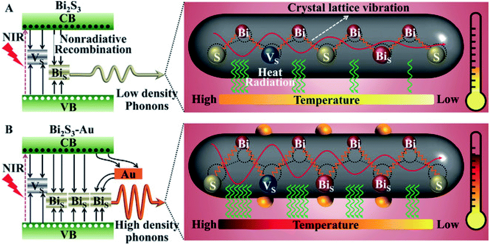 | ||
| Fig. 17 Schematic photothermal mechanism of (A) Bi2S3 NRs and (B) Bi2S3/Au HNSs. On the left side an energy diagram shows the SC band edge absorption, vacancy levels and possible gold incorporation are translated into phonons (crystal lattice vibrations, depicted on the right side) that generate the heat. Reproduced from ref. 386 with permission from Wiley-VCH Verlag GmbH & Co., copyright 2018. | ||
Related reported systems also include other hybrids with insulators or double hydroxides, such as core–shell Au NRs in Al and Mg hydroxides388 and Au NRs partially embedded in silica (Au–SiO2 Janus particle with the Au NR partially exposed) that show improved infrared response for photo-triggered drug delivery alongside improved loading.389 Another advancement was reported by Jiang and co-workers, who have synthesized a material with a strong response in the second NIR window (they measured light penetration at 1064 nm) using Au/Cu9S5 HNS, where both the metal and the semiconductor have an LSPR response.390 A related spherical core@shell Au@Cu2−xE (E = S, Se) was demonstrated by Zhu et al., where the coupling of the plasmonic response of the core and the shell was responsible for high extinction coefficient at 808 nm.391
Huang and co-workers have used the combination of facet-dependent absorption and a plasmonic response to tune photothermal effects of a simple Au–Cu2O system.113 Sun et al. have recently shown a very high photothermal anticancer activity with sub-stoichiometric tungsten trioxide (WO2.9) NRs, which exhibit partial metallic character.392
It is envisioned that this kind of systems can be further enhanced by an HNS formation and other modifications such as cation intercalation (e.g., NH4+).393 Biocompatible magnetic domain-containing HNSs are also promising due to their possible magnetic-controllable catch and release, as demonstrated for Au– and FePt–Fe3O4 heterodimers,394 and multimodal imaging using M/Fe3O4.108
5. Perspective
This review presents the synthesis and applications of diverse types of colloidal hybrid metal–semiconductor nanostructures reported over the last several years. One of the significant challenges in this field is the ability to design and increase the functionality of the single nanostructure. The recent advances in the development of multifunctional materials by interfacing multiple types of materials within a single nanoparticle entity are truly promising but still challenging and have to be further explored. Controlling the properties and the functionalities of nanostructures requires primarily a comprehensible knowledge of the material interfacing mechanism of the sought-after hybrid nanostructure. Thankfully, due to the enormous combinations of diverse hybrid nanomaterials, the scientific community has gained a better insight into the thermodynamic and kinetic parameters, which influence the formation and growth of the hybrid nanomaterials, on the road to develop new multi-component systems with increasing complexity.Further mechanistic elucidation is expected in the near future with the wide-spreading use of advanced electron microscopy techniques. Liquid-phase in situ TEM that allows continuous monitoring has made a significant progress in the elucidation of various metallic NP formation395–397 and transformation,398,399 as well as other inorganic materials.400–405 Other related fields such as superlattice self-assembly from NPs are also treated.406 Though some studies dealing with HNSs exist,407,408 we envision that a more extensive application of these techniques would thrive, mainly when applied to lower-temperature reactions and some technical limitations (see, for example, a tutorial by De Yoreo and co-workers)409 are solved.
Another aspect of characterization is the new information gained using aberration-corrected TEM or STEM: the atomic resolution was already applied to gain mechanistic insight for questions such as SC growth kinetics,410 structural evolution by atom diffusion,411 surface reconstruction,185 composition and bonding in multilayer or multivalent oxides,412 crystal structures of growing 1D materials from metallic catalysts (though usually in gas-phase syntheses),413,414 defects in 2D materials,415 liquid metal/metal-nitride interfaces416 and structural changes on the atomic level of SC NRs/M tips.417 We expect that its use would expand and allow further understanding of reaction intermediates.
Additionally, advanced analytical microscopy techniques coupled to the microscope will shed light on optical and optoelectronic properties.418 Advances in electron energy loss spectroscopy (EELS, used in STEM),419 in particular, could give further insight on the connection between composition (e.g., doping levels, oxidation states)420 and electronic structure (bandgap, plasmon frequencies, etc.421–423), temporal transformation of chemical properties424 and atomic-resolution of interfaces of complex nanostructures.425 Off-axis electron holography could provide detailed electrostatic maps when heterojunctions are formed426 or ions are incorporated,427 providing priceless information for electronic devices. 3D tomography would allow answering intriguing questions regarding surface structure, as pointed out in a review by Miao and co-workers.428
Since intermediate characterization is vital in mechanistic studies, it will not be limited to electron microscopy, and we expect other in situ techniques (e.g., X-ray,429,430 optical spectroscopy431–434) to gain traction alongside the growing use of multimodal imaging.435
The integration of hybrid nanostructures in various devices and applications depends tremendously on the progress that is achieved in two directions: simplifying and reducing the synthesis costs and also developing heavy metal-free (abundant and nontoxic elements) and stable hybrid nanostructures; these are yet to emerge.
Much effort is spent to achieve this goal, and we believe that combination of the mechanistic understanding of colloidal nano-synthesis with emphasis on earth-abundant and nontoxic materials44 alongside the advances of rational (complex) heterostructure design, discussed in this review, makes using hybrid nanoparticles in a wide range of applications definitely feasible and promising.
Conflicts of interest
There are no conflicts to declare.List of abbreviations
| CB | Conduction band |
| e− | Electron |
| fcc | Face-centered cubic |
| h+ | Hole |
| HAADF | High-angle annular dark field |
| HER | Hydrogen evolution reaction |
| HNS | Hybrid nanostructure |
| ITO | Indium tin oxide |
| LSPR | Localized surface plasmon resonance |
| M | Metal |
| NC | Nanocrystal |
| NF | Nickel foam |
| NIR | Near-infrared |
| NPL | Nanoplate or nanoplatelet |
| NR | Nanorod |
| NW | Nanowire |
| OER | Oxygen evolution reaction |
| ORR | Oxygen reduction reaction |
| PCE | Photon-to-electron conversion efficiency |
| PEC | Photoelectrochemical cell |
| QD | Quantum dot |
| rt | Room temperature (25 °C) |
| SC | Semiconductor |
| SLS | Solution–liquid–solid |
| SSP | Single-source precursor |
| STEM | Scanning transmission electron microscopy |
| TEM | Transmission electron microscopy |
| TM | Transition-metal |
| TMP | Transition-metal phosphide |
| VB | Valance band |
| vdW | van der Waals |
| VLS | Vapor–liquid–solid |
Chemicals and reagents
| acac | Acetylacetonate |
| DDA | Dodecylamine |
| DDAB | Didodecyldimethylammonium bromide |
| DDT | Dodecanethiol |
| DTAB | n-Dodecyltrimethylammonium bromide |
| EtOH | Ethanol |
| MB | Methylene blue |
| MeCN | Acetonitrile |
| MO | Methyl orange |
| MPA | Mercaptopropionic acid |
| MUA | Mercaptoundecanoic acid |
| 4-NP: | 4-Nitrophenol |
| OA | Oleic acid |
| OY | Oleylamine |
| PEDOT:PSS | Poly(3,4-ethylenedioxythiophene) polystyrene sulfonate |
| PVP | Polyvinylpyrrolidone |
| RhB | Rhodamine B |
| Rh6G | Rhodamine 6G |
References
- C. B. Murray, D. J. Norris and M. G. Bawendi, J. Am. Chem. Soc., 1993, 115, 8706–8715 CrossRef CAS.
- M. V. Kovalenko, L. Manna, A. Cabot, Z. Hens, D. V. Talapin, C. R. Kagan, V. I. Klimov, A. L. Rogach, P. Reiss, D. J. Milliron, P. Guyot-Sionnnest, G. Konstantatos, W. J. Parak, T. Hyeon, B. A. Korgel, C. B. Murray and W. Heiss, ACS Nano, 2015, 9, 1012–1057 CrossRef CAS PubMed.
- Y. Hong, Y. Wu, S. Wu, X. Wang and J. Zhang, Isr. J. Chem., 2019, 59, 661–672 CrossRef CAS.
- C. R. Kagan, E. Lifshitz, E. H. Sargent and D. V. Talapin, Science, 2016, 353, aac5523 CrossRef PubMed.
- D. V. Talapin and E. V. Shevchenko, Chem. Rev., 2016, 116, 10343–10345 CrossRef CAS.
- J. van Embden, A. S. R. Chesman and J. J. Jasieniak, Chem. Mater., 2015, 27, 2246–2285 CrossRef CAS.
- J. Lee, J. Yang, S. G. Kwon and T. Hyeon, Nat. Rev. Mater., 2016, 1, 16034 CrossRef CAS.
- S. G. Kwon and T. Hyeon, Small, 2011, 7, 2685–2702 CrossRef CAS.
- J. Park, J. Joo, S. G. Kwon, Y. Jang and T. Hyeon, Angew. Chem., Int. Ed., 2007, 46, 4630–4660 CrossRef CAS PubMed.
- M. A. Hines and P. Guyot-Sionnest, J. Phys. Chem., 1996, 100, 468–471 CrossRef CAS.
- O. Chen, J. Zhao, V. P. Chauhan, J. Cui, C. Wong, D. K. Harris, H. Wei, H. S. Han, D. Fukumura, R. K. Jain and M. G. Bawendi, Nat. Mater., 2013, 12, 445–451 CrossRef CAS PubMed.
- S. Jun and E. Jang, Angew. Chem., Int. Ed., 2013, 52, 679–682 CrossRef.
- S. Kim, B. Fisher, H.-J. Eisler and M. Bawendi, J. Am. Chem. Soc., 2003, 125, 11466–11467 CrossRef.
- A. Aharoni, T. Mokari, I. Popov and U. Banin, J. Am. Chem. Soc., 2006, 128, 257–264 CrossRef.
- P. Jing, J. Zheng, M. Ikezawa, X. Liu, S. Lv, X. Kong, J. Zhao and Y. Masumoto, J. Phys. Chem. C, 2009, 113, 13545–13550 CrossRef.
- P. Reiss, M. Protière and L. Li, Small, 2009, 5, 154–168 CrossRef.
- F. Gao, M. Kaneko, C. D. Heyes, P. Bajwa and B. Omogo, ACS Nano, 2016, 10, 4072–4082 CrossRef.
- Y. Jang, A. Shapiro, F. Horani, A. Abu-Hariri and E. Lifshitz, J. Phys. Chem. C, 2018, 122, 13840–13847 CrossRef CAS.
- J. Liu, S. Z. Qiao, J. S. Chen, X. W. Lou, X. Xing and G. Q. Lu, Chem. Commun., 2011, 47, 12578 RSC.
- R. Purbia and S. Paria, Nanoscale, 2015, 7, 19789–19873 RSC.
- A. Li, W. Zhu, C. Li, T. Wang and J. Gong, Chem. Soc. Rev., 2019, 48, 1874–1907 RSC.
- T. Teranishi and M. Sakamoto, J. Phys. Chem. Lett., 2013, 4, 2867–2873 CrossRef.
- K.-W. Kwon and M. Shim, J. Am. Chem. Soc., 2005, 127, 10269–10275 CrossRef.
- M. Saruyama, Y.-G. So, K. Kimoto, S. Taguchi, Y. Kanemitsu and T. Teranishi, J. Am. Chem. Soc., 2011, 133, 17598–17601 CrossRef.
- S.-H. Choi, E.-G. Kim and T. Hyeon, J. Am. Chem. Soc., 2006, 128, 2520–2521 CrossRef.
- D. V. Talapin, J. H. Nelson, E. V. Shevchenko, S. Aloni, B. Sadtler and A. P. Alivisatos, Nano Lett., 2007, 7, 2951–2959 CrossRef PubMed.
- A. Fiore, R. Mastria, M. G. Lupo, G. Lanzani, C. Giannini, E. Carlino, G. Morello, M. De Giorgi, Y. Li, R. Cingolani and L. Manna, J. Am. Chem. Soc., 2009, 131, 2274–2282 CrossRef PubMed.
- S. Deka, K. Miszta, D. Dorfs, A. Genovese, G. Bertoni and L. Manna, Nano Lett., 2010, 10, 3770–3776 CrossRef PubMed.
- H. Zhong and G. D. Scholes, J. Am. Chem. Soc., 2009, 131, 9170–9171 CrossRef.
- A. J. Mieszawska, R. Jalilian, G. U. Sumanasekera and F. P. Zamborini, Small, 2007, 3, 722–756 CrossRef PubMed.
- Y. Xia, P. Yang, Y. Sun, Y. Wu, B. Mayers, B. Gates, Y. Yin, F. Kim and H. Yan, Adv. Mater., 2003, 15, 353–389 CrossRef.
- H. Li, A. G. Kanaras and L. Manna, Acc. Chem. Res., 2013, 46, 1387–1396 CrossRef.
- Y. E. Panfil, M. Oded and U. Banin, Angew. Chem., Int. Ed., 2018, 57, 4274–4295 CrossRef.
- A. Teitelboim, N. Meir, M. Kazes and D. Oron, Acc. Chem. Res., 2016, 49, 902–910 CrossRef.
- A. Vilan and D. Cahen, Chem. Rev., 2017, 117, 4624–4666 CrossRef.
- K. L. Kelly, E. Coronado, L. L. Zhao and G. C. Schatz, J. Phys. Chem. B, 2003, 107, 668–677 CrossRef.
- W. E. Buhro and V. L. Colvin, Nat. Mater., 2003, 2, 138–139 CrossRef.
- A. P. Alivisatos, Science, 1996, 271, 933–937 CrossRef.
- H. Zhu, Z. Fan, L. Yu, M. A. Wilson, Y. Nagaoka, D. Eggert, C. Cao, Y. Liu, Z. Wei, X. Wang, J. He, J. Zhao, R. Li, Z. Wang, M. Grünwald and O. Chen, J. Am. Chem. Soc., 2019, 141, 6013–6021 CrossRef PubMed.
- J. Quiroz, E. C. M. Barbosa, T. P. Araujo, J. L. Fiorio, Y.-C. Wang, Y.-C. Zou, T. Mou, T. V. Alves, D. C. de Oliveira, B. Wang, S. J. Haigh, L. M. Rossi and P. H. C. Camargo, Nano Lett., 2018, 18, 7289–7297 CrossRef.
- U. Banin, Y. Ben-Shahar and K. Vinokurov, Chem. Mater., 2014, 26, 97–110 CrossRef.
- S. K. Dutta, S. K. Mehetor and N. Pradhan, J. Phys. Chem. Lett., 2015, 6, 936–944 CrossRef.
- N. Razgoniaeva, P. Moroz, S. Lambright and M. Zamkov, J. Phys. Chem. Lett., 2015, 6, 4352–4359 CrossRef.
- P. Reiss, M. Carrière, C. Lincheneau, L. Vaure and S. Tamang, Chem. Rev., 2016, 116, 10731–10819 CrossRef CAS.
- L. Carbone and P. D. Cozzoli, Nano Today, 2010, 5, 449–493 CrossRef CAS.
- R. Scarfiello, C. Nobile and P. D. Cozzoli, Front. Mater., 2016, 3, 1–29 Search PubMed.
- P. D. Cozzoli, T. Pellegrino and L. Manna, Chem. Soc. Rev., 2006, 35, 1195–1208 RSC.
- R. Costi, A. E. Saunders and U. Banin, Angew. Chem., Int. Ed., 2010, 49, 4878–4897 CrossRef CAS.
- C. Tan, J. Chen, X.-J. Wu and H. Zhang, Nat. Rev. Mater., 2018, 3, 17089 CrossRef CAS.
- M. R. Buck, J. F. Bondi and R. E. Schaak, Nat. Chem., 2012, 4, 37–44 CrossRef CAS PubMed.
- M. R. Buck and R. E. Schaak, Angew. Chem., Int. Ed., 2013, 52, 6154–6178 CrossRef CAS PubMed.
- K. D. Gilroy, A. Ruditskiy, H.-C. Peng, D. Qin and Y. Xia, Chem. Rev., 2016, 116, 10414–10472 CrossRef PubMed.
- I. Kriegel, F. Scotognella and L. Manna, Phys. Rep., 2017, 674, 1–52 CrossRef.
- S. Karthika, T. K. Radhakrishnan and P. Kalaichelvi, Cryst. Growth Des., 2016, 16, 6663–6681 CrossRef.
- B. Ma, C. Kong, J. Lv, W. Zhang, J. Guo, X. Zhang, Z. Yang and S. Yang, ChemistrySelect, 2018, 3, 10641–10645 CrossRef.
- J. D. S. Newman and G. J. Blanchard, Langmuir, 2006, 22, 5882–5887 CrossRef PubMed.
- S. Deka, A. Falqui, G. Bertoni, C. Sangregorio, G. Poneti, G. Morello, M. De Giorgi, C. Giannini, R. Cingolani, L. Manna and P. D. Cozzoli, J. Am. Chem. Soc., 2009, 131, 12817–12828 CrossRef PubMed.
- C. Pacholski, A. Kornowski and H. Weller, Angew. Chem., Int. Ed., 2004, 43, 4774–4777 CrossRef CAS PubMed.
- G. Dukovic, M. G. Merkle, J. H. Nelson, S. M. Hughes and A. P. Alivisatos, Adv. Mater., 2008, 20, 4306–4311 CrossRef CAS.
- K. X. Yao, X. Liu, L. Zhao, H. C. Zeng and Y. Han, Nanoscale, 2011, 3, 4195 RSC.
- M. D. Ballentine, E. G. Embry, M. A. Garcia and L. J. Hill, Beilstein J. Nanotechnol., 2019, 10, 718–724 CrossRef CAS.
- L. Carbone, A. Jakab, Y. Khalavka and C. Sönnichsen, Nano Lett., 2009, 9, 3710–3714 CrossRef CAS PubMed.
- J. F. S. Fernando, M. P. Shortell, C. J. Noble, J. R. Harmer, E. A. Jaatinen and E. R. Waclawik, ACS Appl. Mater. Interfaces, 2016, 8, 14271–14283 CrossRef CAS.
- J. F. S. Fernando, M. P. Shortell, K. L. Firestein, C. Zhang, K. V. Larionov, Z. I. Popov, P. B. Sorokin, L. Bourgeois, E. R. Waclawik and D. V. Golberg, Langmuir, 2018, 34, 7334–7345 CrossRef CAS.
- Y. Ge, T. Wang, M. Zheng, Z. Jiang and S. Wang, Nanotechnology, 2019, 30, 315702 CrossRef.
- X. Chen, W. Chen, P. Lin, Y. Yang, H. Gao, J. Yuan and W. Shangguan, Catal. Commun., 2013, 36, 104–108 CrossRef CAS.
- Z. Chai, T.-T. Zeng, Q. Li, L.-Q. Lu, W.-J. Xiao and D. Xu, J. Am. Chem. Soc., 2016, 138, 10128–10131 CrossRef CAS.
- M. Zhukovskyi, P. Tongying, H. Yashan, Y. Wang and M. Kuno, ACS Catal., 2015, 5, 6615–6623 CrossRef CAS.
- T. Simon, N. Bouchonville, M. J. Berr, A. Vaneski, A. Adrović, D. Volbers, R. Wyrwich, M. Döblinger, A. S. Susha, A. L. Rogach, F. Jäckel, J. K. Stolarczyk and J. Feldmann, Nat. Mater., 2014, 13, 1013–1018 CrossRef CAS.
- B. Mahler, L. Guillemot, L. Bossard-Giannesini, S. Ithurria, D. Pierucci, A. Ouerghi, G. Patriarche, R. Benbalagh, E. Lacaze, F. Rochet and E. Lhuillier, J. Phys. Chem. C, 2016, 120, 12351–12361 CrossRef CAS.
- A. Manzi, T. Simon, C. Sonnleitner, M. Döblinger, R. Wyrwich, O. Stern, J. K. Stolarczyk and J. Feldmann, J. Am. Chem. Soc., 2015, 137, 14007–14010 CrossRef CAS.
- T. Mokari, Science, 2004, 304, 1787–1790 CrossRef CAS.
- T. Mokari, C. G. Sztrum, A. Salant, E. Rabani and U. Banin, Nat. Mater., 2005, 4, 855–863 CrossRef CAS.
- T. Mokari, R. Costi, C. G. Sztrum, E. Rabani and U. Banin, Phys. Status Solidi, 2006, 243, 3952–3958 CrossRef CAS.
- A. E. Saunders, I. Popov and U. Banin, J. Phys. Chem. B, 2006, 110, 25421–25429 CrossRef CAS.
- S. E. Habas, P. Yang and T. Mokari, J. Am. Chem. Soc., 2008, 130, 3294–3295 CrossRef CAS.
- K. Ahrenstorf, O. Albrecht, H. Heller, A. Kornowski, D. Görlitz and H. Weller, Small, 2007, 3, 271–274 CrossRef CAS.
- B. D. Yuhas, S. E. Habas, S. C. Fakra and T. Mokari, ACS Nano, 2009, 3, 3369–3376 CrossRef CAS.
- H. Schlicke, D. Ghosh, L.-K. Fong, H. L. Xin, H. Zheng and A. P. Alivisatos, Angew. Chem., Int. Ed., 2013, 52, 980–982 CrossRef.
- M. Meyns, N. G. Bastus, Y. Cai, A. Kornowski, B. H. Juárez, H. Weller and C. Klinke, J. Mater. Chem., 2010, 20, 10602 RSC.
- T. Okuhata, Y. Kobayashi, Y. Nonoguchi, T. Kawai and N. Tamai, J. Phys. Chem. C, 2015, 119, 2113–2120 CrossRef.
- J. Yang, E. Sargent, S. Kelley and J. Y. Ying, Nat. Mater., 2009, 8, 683–689 CrossRef.
- I. R. Franchini, G. Bertoni, A. Falqui, C. Giannini, L. W. Wang and L. Manna, J. Mater. Chem., 2010, 20, 1357–1366 RSC.
- M. Dalmases, M. Ibáñez, P. Torruella, V. Fernàndez-Altable, L. López-Conesa, D. Cadavid, L. Piveteau, M. Nachtegaal, J. Llorca, M. L. Ruiz-González, S. Estradé, F. Peiró, M. V. Kovalenko, A. Cabot and A. Figuerola, Chem. Mater., 2016, 28, 7017–7028 CrossRef.
- X. Yu, A. Shavel, X. An, Z. Luo, M. Ibáñez and A. Cabot, J. Am. Chem. Soc., 2014, 136, 9236–9239 CrossRef CAS.
- P. S. Dilsaver, M. D. Reichert, B. L. Hallmark, M. J. Thompson and J. Vela, J. Phys. Chem. C, 2014, 118, 21226–21234 CrossRef CAS.
- A. Ganai, P. S. Maiti, L. Houben, R. Bar-Ziv and M. Bar Sadan, J. Phys. Chem. C, 2017, 121, 7062–7068 CrossRef CAS.
- X. Yu, R. Du, B. Li, L. Liu and Y. Zhang, J. Phys. Chem. C, 2017, 121, 6712–6720 CrossRef CAS.
- E. A. Hernández-Pagán, A. D. P. Leach, J. M. Rhodes, S. Sarkar and J. E. Macdonald, Chem. Mater., 2015, 27, 7969–7976 CrossRef.
- P. Rukenstein, A. Teitelboim, M. Volokh, M. Diab, D. Oron and T. Mokari, J. Phys. Chem. C, 2016, 120, 15453–15459 CrossRef.
- Y. Nakibli, Y. Mazal, Y. Dubi, M. Wächtler and L. Amirav, Nano Lett., 2018, 18, 357–364 CrossRef.
- B. Li, Y. Zhang, R. Du, L. Gan and X. Yu, Langmuir, 2016, 32, 11639–11645 CrossRef.
- S. Naskar, A. Schlosser, J. F. Miethe, F. Steinbach, A. Feldhoff and N. C. Bigall, Chem. Mater., 2015, 27, 3159–3166 CrossRef.
- H. Chauhan, Y. Kumar, J. Dana, B. Satpati, H. N. Ghosh and S. Deka, Nanoscale, 2016, 8, 15802–15812 RSC.
- S. Naskar, F. Lübkemann, S. Hamid, A. Freytag, A. Wolf, J. Koch, I. Ivanova, H. Pfnür, D. Dorfs, D. W. Bahnemann and N. C. Bigall, Adv. Funct. Mater., 2017, 27, 1604685 CrossRef.
- Q. Li, F. Zhao, C. Qu, Q. Shang, Z. Xu, L. Yu, J. R. McBride and T. Lian, J. Am. Chem. Soc., 2018, 140, 11726–11734 CrossRef.
- H. Fridman, L. Tian, K. Shreteh, M. Volokh and T. Mokari, Front. Mater., 2020, 6, 345 CrossRef.
- S.-Y. Tang, H. Medina, Y.-T. Yen, C.-W. Chen, T.-Y. Yang, K.-H. Wei and Y.-L. Chueh, Small, 2019, 15, 1803529 CrossRef.
- E. P. Lazareva, V. F. Kozlovskii, R. B. Vasiliev and A. M. Gaskov, Russ. J. Inorg. Chem., 2018, 63, 642–646 CrossRef.
- Y. Ben-Shahar, F. Scotognella, I. Kriegel, L. Moretti, G. Cerullo, E. Rabani and U. Banin, Nat. Commun., 2016, 7, 10413 CrossRef.
- J. Maynadié, A. Salant, A. Falqui, M. Respaud, E. Shaviv, U. Banin, K. Soulantica and B. Chaudret, Angew. Chem., Int. Ed., 2009, 48, 1814–1817 CrossRef.
- A. B. Ghosh, N. Saha, A. Sarkar, A. K. Dutta, J. Satra and B. Adhikary, Dalton Trans., 2018, 47, 1071–1081 RSC.
- O. Kluge, I. J.-L. Plante, M. Diab, M. Volokh, A. Teitelboim and T. Mokari, J. Mater. Chem. C, 2015, 3, 4657–4662 RSC.
- Q. Tan, C. Du, Y. Sun, G. Yin and Y. Gao, J. Mater. Chem. A, 2014, 2, 1429–1435 RSC.
- T. Bala, A. Singh, A. Sanyal, C. O'Sullivan, F. Laffir, C. Coughlan and K. M. Ryan, Nano Res., 2013, 6, 121–130 CrossRef.
- L. J. Zhang, R. Zheng, S. Li, B. K. Liu, D. J. Wang, L. L. Wang and T. F. Xie, ACS Appl. Mater. Interfaces, 2014, 6, 13406–13412 CrossRef.
- S. Das, B. Satpati, H. Chauhan, S. Deka, M. K. Ghosalya, C. S. Gopinath and T. Bala, RSC Adv., 2016, 6, 14658–14665 RSC.
- J. Zeng, M. Gong, D. Wang, M. Li, W. Xu, Z. Li, S. Li, D. Zhang, Z. Yan and Y. Yin, Nano Lett., 2019, 19, 3011–3018 CrossRef.
- H. Wang, D. W. Brandl, F. Le, P. Nordlander and N. J. Halas, Nano Lett., 2006, 6, 827–832 CrossRef CAS.
- M. Chang, M. Wang, Y. Chen, M. Shu, Y. Zhao, B. Ding, Z. Hou and J. Lin, Nanoscale, 2019, 11, 10129–10136 RSC.
- C. Kuo, T. Hua and M. H. Huang, J. Am. Chem. Soc., 2009, 131, 17871–17878 CrossRef CAS.
- W. Wang, L. Lyu and M. H. Huang, Chem. Mater., 2011, 23, 2677–2684 CrossRef CAS.
- H. Wang, K. Yang, S. Hsu and M. H. Huang, Nanoscale, 2016, 8, 965–972 RSC.
- S. Rej, H. Wang, M.-X. Huang, S. Hsu, C. Tan, F. Lin, J.-S. Huang and M. H. Huang, Nanoscale, 2015, 7, 11135–11141 RSC.
- K. Yang, S. Hsu and M. H. Huang, Chem. Mater., 2016, 28, 5140–5146 CrossRef CAS.
- C.-F. Hsia, C.-H. Chang and M. H. Huang, Part. Part. Syst. Charact., 2018, 35, 1800112 CrossRef.
- N. Meir, I. Jen-La Plante, K. Flomin, E. Chockler, B. Moshofsky, M. Diab, M. Volokh and T. Mokari, J. Mater. Chem. A, 2013, 1, 1763–1769 RSC.
- H. Jing, N. Large, Q. Zhang and H. Wang, J. Phys. Chem. C, 2014, 118, 19948–19963 CrossRef CAS.
- C. Kuo and M. H. Huang, J. Am. Chem. Soc., 2008, 130, 12815–12820 CrossRef CAS.
- B. Lu, A. Liu, H. Wu, Q. Shen, T. Zhao and J. Wang, Langmuir, 2016, 32, 3085–3094 CrossRef CAS.
- S. Zhang, R. Jiang, Y. Guo, B. Yang, X.-L. Chen, J. Wang and Y. Zhao, Small, 2016, 12, 4264–4276 CrossRef CAS.
- L. Zhang, D. A. Blom and H. Wang, Chem. Mater., 2011, 23, 4587–4598 CrossRef CAS.
- M. H. Huang, Small, 2019, 15, 1804726 CrossRef.
- J. Li, S. K. Cushing, J. Bright, F. Meng, T. R. Senty, P. Zheng, A. D. Bristow and N. Wu, ACS Catal., 2013, 3, 47–51 CrossRef CAS.
- S. K. Cushing, J. Li, F. Meng, T. R. Senty, S. Suri, M. Zhi, M. Li, A. D. Bristow and N. Wu, J. Am. Chem. Soc., 2012, 134, 15033–15041 CrossRef CAS PubMed.
- C. Tao, L. An, J. Lin, Q. Tian and S. Yang, Small, 2019, 15, 1903473 CrossRef CAS.
- Y. Lv, S. Duan, Y. Zhu, H. Guo and R. Wang, Chem. Eng. J., 2020, 382, 122794 CrossRef CAS.
- S. Javaid, Y. Li, D. Chen, X. Xu, Y. Pang, W. Chen, F. Wang, Z. Shao, M. Saunders, J.-P. Veder, G. Jia and F. Jones, J. Phys. Chem. C, 2019, 123, 10604–10613 CrossRef CAS.
- B. K. Patra, S. Khilari, D. Pradhan and N. Pradhan, Chem. Mater., 2016, 28, 4358–4366 CrossRef CAS.
- F. Vita, C. Innocenti, A. Secchi, F. Albertini, V. Grillo, A. Fiore, P. D. Cozzoli and C. de Julián Fernández, J. Mater. Chem. C, 2018, 6, 12329–12340 RSC.
- J. F. S. Fernando, M. P. Shortell, K. C. Vernon, E. A. Jaatinen and E. R. Waclawik, Cryst. Growth Des., 2015, 15, 4324–4330 CrossRef CAS.
- D. Zeng, P. Gong, Y. Chen, Q. Zhang, Q. Xie and D.-L. Peng, Nanoscale, 2016, 8, 11602–11610 RSC.
- T. R. Gordon and R. E. Schaak, Chem. Mater., 2014, 26, 5900–5904 CrossRef CAS.
- C. W. Li and M. W. Kanan, J. Am. Chem. Soc., 2012, 134, 7231–7234 CrossRef CAS.
- S. Lee, D. Kim and J. Lee, Angew. Chem., Int. Ed., 2015, 54, 14701–14705 CrossRef CAS.
- M. Verelst, T. O. Ely, C. Amiens, E. Snoeck, P. Lecante, A. Mosset, M. Respaud, J. M. Broto and B. Chaudret, Chem. Mater., 1999, 11, 2702–2708 CrossRef CAS.
- W. Liu, L. Chen, L. Cui, J. Yan, S. Zhang and S. Shi, J. Mater. Chem. A, 2019, 7, 15089–15100 RSC.
- M. Casavola, R. Buonsanti, G. Caputo and P. D. Cozzoli, Eur. J. Inorg. Chem., 2008, 837–854 CrossRef CAS.
- L.-I. Hung, C.-K. Tsung, W. Huang and P. Yang, Adv. Mater., 2010, 22, 1910–1914 CrossRef CAS.
- X. Zhu, H. Rong, X. Zhang, Q. Di, H. Shang, B. Bai, J. Liu, J. Liu, M. Xu, W. Chen and J. Zhang, Nano Res., 2019, 12, 1187–1192 CrossRef CAS.
- Y. Yin, R. M. Rioux, C. K. Erdonmez, S. Hughes, G. A. Somorjai and P. A. Alivisatos, Science, 2004, 304, 711–714 CrossRef CAS.
- J. B. Tracy, D. N. Weiss, D. P. Dinega and M. G. Bawendi, Phys. Rev. B: Condens. Matter Mater. Phys., 2005, 72, 064404 CrossRef.
- J. Ustarroz, M. Kang, E. Bullions and P. R. Unwin, Chem. Sci., 2017, 8, 1841–1853 RSC.
- X. Wang, G. Liu, L. Wang, Z.-G. Chen, G. Q. M. Lu and H.-M. Cheng, Adv. Energy Mater., 2012, 2, 42–46 CrossRef.
- F. Nan, S. Liang, J.-H. Wang, X.-L. Liu, D.-J. Yang, X.-F. Yu, L. Zhou, Z.-H. Hao and Q.-Q. Wang, Adv. Opt. Mater., 2014, 2, 679–686 CrossRef.
- N. E. Motl, J. F. Bondi and R. E. Schaak, Chem. Mater., 2012, 24, 1552–1554 CrossRef.
- S. U. Lee, J. W. Hong, S. Il Choi and S. W. Han, J. Am. Chem. Soc., 2014, 136, 5221–5224 CrossRef.
- M. L. Nguyen, J. A. Murphy, L. C. Hamlet and B. L. T. Lau, Environ. Sci.: Nano, 2018, 5, 1090–1095 RSC.
- Y. Zhang, J. Xia, Y. Liu, L. Qiang and L. Zhu, Environ. Sci. Technol., 2016, 50, 13283–13290 CrossRef.
- J. van Embden, L. Bourgeois, E. Della Gaspera, L. Waddington, Y. Yin, N. V. Medhekar, J. J. Jasieniak and A. S. R. Chesman, J. Mater. Chem. A, 2016, 4, 7060–7070 RSC.
- I. du Fossé, S. ten Brinck, I. Infante and A. J. Houtepen, Chem. Mater., 2019, 31, 4575–4583 CrossRef PubMed.
- B. H. R. Suryanto, C. S. M. Kang, D. Wang, C. Xiao, F. Zhou, L. M. Azofra, L. Cavallo, X. Zhang and D. R. MacFarlane, ACS Energy Lett., 2018, 3, 1219–1224 CrossRef CAS.
- M. Jiang, W. Liu, X. Yang, Z. Jiang, T. Yao, S. Wei and X. Peng, ACS Nano, 2015, 9, 10950–10960 CrossRef CAS PubMed.
- B. Wang, S. He, L. Zhang, X. Huang, F. Gao, W. Feng and P. Liu, Appl. Catal., B, 2019, 243, 229–235 CrossRef CAS.
- Z. Wei, F. Yue, Z. Jin, Z. Fengxia, S. Zhenhuan, D. Benlin, D. Y. C. Leung, Z. Lili and X. Jiming, ACS Appl. Energy Mater., 2019, 2, 694–704 CrossRef CAS.
- T. J. Trentler, K. M. Hickman, S. C. Goel, A. M. Viano, P. C. Gibbons and W. E. Buhro, Science, 1995, 270, 1791–1794 CrossRef CAS.
- T. Hanrath and B. A. Korgel, J. Am. Chem. Soc., 2002, 124, 1424–1429 CrossRef CAS PubMed.
- S. Kan, A. Aharoni, T. Mokari and U. Banin, Faraday Discuss., 2004, 125, 23–38 RSC.
- S. Kan, T. Mokari, E. Rothenberg and U. Banin, Nat. Mater., 2003, 2, 155–158 CrossRef CAS PubMed.
- T. J. Trentler, S. C. Goel, K. M. Hickman, A. M. Viano, M. Y. Chiang, A. M. Beatty, P. C. Gibbons and W. E. Buhro, J. Am. Chem. Soc., 1997, 119, 2172–2181 CrossRef CAS.
- K.-T. Yong, Y. Sahoo, K. R. Choudhury, M. T. Swihart, J. R. Minter and P. N. Prasad, Chem. Mater., 2006, 18, 5965–5972 CrossRef CAS.
- J. Sun and W. E. Buhro, Angew. Chem., 2008, 120, 3259–3262 CrossRef.
- A. T. Heitsch, C. M. Hessel, V. A. Akhavan and B. A. Korgel, Nano Lett., 2009, 9, 3042–3047 CrossRef CAS PubMed.
- F. Wang, A. Dong, J. Sun, R. Tang, H. Yu and W. E. Buhro, Inorg. Chem., 2006, 45, 7511–7521 CrossRef CAS PubMed.
- I. Jen-La Plante, S. E. Habas, B. D. Yuhas, D. J. Gargas and T. Mokari, Chem. Mater., 2009, 21, 3662–3667 CrossRef CAS.
- Y. Wang and Y. Xia, Nano Lett., 2004, 4, 2047–2050 CrossRef CAS.
- J. M. De Corrado, J. F. S. Fernando, M. P. Shortell, B. L. J. Poad, S. J. Blanksby and E. R. Waclawik, ACS Appl. Nano Mater., 2019, 2, 7856–7869 CrossRef CAS.
- Y. Chen, D. Zeng, M. B. Cortie, A. Dowd, H. Guo, J. Wang and D.-L. Peng, Small, 2015, 11, 1460–1469 CrossRef PubMed.
- K. Flomin, I. Jen-La Plante, B. Moshofsky, M. Diab and T. Mokari, Nanoscale, 2014, 6, 1335–1339 RSC.
- X.-B. Xiang, Y. Yu, W. Wen and J.-M. Wu, New J. Chem., 2018, 42, 265–271 RSC.
- Y. Tang, H. Ruan, H. Liu, J. Zhang, D. Shi, T. Han and L. Yang, J. Alloys Compd., 2018, 747, 659–665 CrossRef.
- W. J. Plieth, J. Electroanal. Chem. Interfacial Electrochem., 1986, 204, 343–349 CrossRef.
- L. De La Cueva, M. Meyns, N. G. Bastús, J. Rodríguez-Fernández, R. Otero, J. M. Gallego, C. Alonso, C. Klinke and B. H. Juárez, Chem. Mater., 2016, 28, 2704–2714 CrossRef CAS.
- Y. Min, J. Kwak, A. Soon and U. Jeong, Acc. Chem. Res., 2014, 47, 2887–2893 CrossRef CAS PubMed.
- R. Weichelt, J. Ye, U. Banin, A. Eychmüller and R. Seidel, Chem.–Eur. J., 2019, 25, 9012–9016 CrossRef CAS PubMed.
- X.-J. Lin, T.-Q. Sun, L.-P. Yang, Y.-G. Sun, D.-S. Bin, S.-Y. Duan, Y. Liu, R.-W. Lv and A.-M. Cao, Chem. Commun., 2019, 55, 1076–1079 RSC.
- L. De Trizio and L. Manna, Chem. Rev., 2016, 116, 10852–10887 CrossRef CAS PubMed.
- J. L. Fenton, J. M. Hodges and R. E. Schaak, Chem. Mater., 2017, 29, 6168–6177 CrossRef CAS.
- X. Shi, S. Posysaev, M. Huttula, V. Pankratov, J. Hoszowska, J.-C. Dousse, F. Zeeshan, Y. Niu, A. Zakharov, T. Li, O. Miroshnichenko, M. Zhang, X. Wang, Z. Huang, S. Saukko, D. L. González, S. van Dijken, M. Alatalo and W. Cao, Small, 2018, 14, 1704526 CrossRef PubMed.
- Y. Liu, Y. Huang and X. Duan, Nature, 2019, 567, 323–333 CrossRef CAS PubMed.
- G. Konstantatos, M. Badioli, L. Gaudreau, J. Osmond, M. Bernechea, F. P. G. de Arquer, F. Gatti and F. H. L. Koppens, Nat. Nanotechnol., 2012, 7, 363–368 CrossRef CAS PubMed.
- Z. Xu, J. Park, G. Yoon, H. Kim and K. Kang, Small Methods, 2019, 3, 1800227 CrossRef CAS.
- D. Kwak, P. Ramasamy, Y.-S. Lee, M.-H. Jeong and J.-S. Lee, ACS Appl. Mater. Interfaces, 2019, 11, 29041–29046 CrossRef CAS PubMed.
- S. Yang, G. Chen, A. G. Ricciardulli, P. Zhang, Z. Zhang, H. Shi, J. Ma, J. Zhang, P. W. M. Blom and X. Feng, Angew. Chem., 2020, 132, 473–478 CrossRef.
- P. S. Maiti, A. K. Ganai, R. Bar-Ziv, A. N. Enyashin, L. Houben and M. Bar Sadan, Chem. Mater., 2018, 30, 4489–4492 CrossRef CAS.
- G. Sun, B. Li, J. Li, Z. Zhang, H. Ma, P. Chen, B. Zhao, R. Wu, W. Dang, X. Yang, X. Tang, C. Dai, Z. Huang, Y. Liu, X. Duan and X. Duan, Nano Res., 2019, 12, 1139–1145 CrossRef CAS.
- M. Gao, Y. Yu, W. Yang, J. Li, S. Xu, M. Feng and H. Li, Nanoscale, 2019, 11, 3506–3513 RSC.
- M. Volokh, G. Peng, J. Barrio and M. Shalom, Angew. Chem., Int. Ed., 2019, 58, 6138–6151 CrossRef PubMed.
- D. V. Shtansky, K. L. Firestein and D. V. Golberg, Nanoscale, 2018, 10, 17477–17493 RSC.
- Y. Liu, N. O. Weiss, X. Duan, H.-C. Cheng, Y. Huang and X. Duan, Nat. Rev. Mater., 2016, 1, 16042 CrossRef.
- X. Li, J. Zhu and B. Wei, Chem. Soc. Rev., 2016, 45, 3145–3187 RSC.
- M. Nasilowski, B. Mahler, E. Lhuillier, S. Ithurria and B. Dubertret, Chem. Rev., 2016, 116, 10934–10982 CrossRef PubMed.
- R. Matheu, I. A. Moreno-Hernandez, X. Sala, H. B. Gray, B. S. Brunschwig, A. Llobet and N. S. Lewis, J. Am. Chem. Soc., 2017, 139, 11345–11348 CrossRef PubMed.
- H. Fridman, M. Diab, M. Volokh, A. I. Shames, S. Kolusheva and T. Mokari, Part. Part. Syst. Charact., 2019, 36, 1800452 CrossRef.
- H.-W. Tseng, M. B. Wilker, N. H. Damrauer and G. Dukovic, J. Am. Chem. Soc., 2013, 135, 3383–3386 CrossRef PubMed.
- S. Lian, M. S. Kodaimati, D. S. Dolzhnikov, R. Calzada and E. A. Weiss, J. Am. Chem. Soc., 2017, 139, 8931–8938 CrossRef PubMed.
- J. K. Utterback, M. B. Wilker, D. W. Mulder, P. W. King, J. D. Eaves and G. Dukovic, J. Phys. Chem. C, 2019, 123, 886–896 CrossRef.
- Q. Liu, Z.-X. Low, L. Li, A. Razmjou, K. Wang, J. Yao and H. Wang, J. Mater. Chem. A, 2013, 1, 11563 RSC.
- Q. Yang, Q. Xu and H. L. Jiang, Chem. Soc. Rev., 2017, 46, 4774–4808 RSC.
- K. M. Choi, D. Kim, B. Rungtaweevoranit, C. A. Trickett, J. T. D. Barmanbek, A. S. Alshammari, P. Yang and O. M. Yaghi, J. Am. Chem. Soc., 2017, 139, 356–362 CrossRef CAS PubMed.
- F. Fu, C. Wang, Q. Wang, A. M. Martinez-Villacorta, A. Escobar, H. Chong, X. Wang, S. Moya, L. Salmon, E. Fouquet, J. Ruiz and D. Astruc, J. Am. Chem. Soc., 2018, 140, 10034–10042 CrossRef CAS.
- J. G. Hinman, J. G. Turner, D. M. Hofmann and C. J. Murphy, Chem. Mater., 2018, 30, 7255–7261 CrossRef CAS.
- J.-K. Wu, P. Tan, J. Lu, Y. Jiang, X.-Q. Liu and L.-B. Sun, ACS Appl. Mater. Interfaces, 2019, 11, 29298–29304 CrossRef CAS.
- C. M. Wolff, P. D. Frischmann, M. Schulze, B. J. Bohn, R. Wein, P. Livadas, M. T. Carlson, F. Jäckel, J. Feldmann, F. Würthner and J. K. Stolarczyk, Nat. Energy, 2018, 3, 862–869 CrossRef CAS.
- Z. Han and R. Eisenberg, Acc. Chem. Res., 2014, 47, 2537–2544 CrossRef CAS.
- J. Zhang, B. Tian, L. Wang, M. Xing and J. Lei, in Photocatalysis: Fundamentals, Materials and Applications, Springer Singapore, Singapore, 2018, pp. 375–402 Search PubMed.
- H. Chen, D. Jiang, Z. Sun, R. M. Irfan, L. Zhang and P. Du, Catal. Sci. Technol., 2017, 7, 1515–1522 RSC.
- B. Varghese, B. Mukherjee, K. R. G. Karthik, K. B. Jinesh, S. G. Mhaisalkar, E. Soon Tok and C. Haur Sow, J. Appl. Phys., 2012, 111, 104306 CrossRef.
- F. Tran, P. Blaha, K. Schwarz and P. Novák, Phys. Rev. B: Condens. Matter Mater. Phys., 2006, 74, 155108 CrossRef.
- K.-W. Park and A. M. Kolpak, J. Catal., 2018, 365, 115–124 CrossRef CAS.
- S. Zhu, W. Liao, M. Zhang and S. Liang, Chem. Eng. J., 2019, 361, 461–469 CrossRef CAS.
- Z. Han, F. Qiu, R. Eisenberg, P. L. Holland and T. D. Krauss, Science, 2012, 338, 1321–1324 CrossRef CAS PubMed.
- Z. Khan, M. Khannam, N. Vinothkumar, M. De and M. Qureshi, J. Mater. Chem., 2012, 22, 12090–12095 RSC.
- G. Han, Y.-H. Jin, R. A. Burgess, N. E. Dickenson, X.-M. Cao and Y. Sun, J. Am. Chem. Soc., 2017, 139, 15584–15587 CrossRef CAS PubMed.
- I. Vamvasakis, I. T. Papadas, T. Tzanoudakis, C. Drivas, S. A. Choulis, S. Kennou and G. S. Armatas, ACS Catal., 2018, 8, 8726–8738 CrossRef CAS.
- L. Zhang, G. Wang and Z. Jin, New J. Chem., 2019, 43, 6411–6421 RSC.
- Y. Lu, T. Wang, X. Li, G. Zhang, H. Xue and H. Pang, RSC Adv., 2016, 6, 87188–87212 RSC.
- S. Cao, Y. Chen, C. Wang, X. Lv and W.-F. Fu, Chem. Commun., 2015, 51, 8708–8711 RSC.
- Q. Yue, Y. Wan, Z. Sun, X. Wu, Y. Yuan and P. Du, J. Mater. Chem. A, 2015, 3, 16941–16947 RSC.
- Y.-H. Li, M.-Y. Qi, J.-Y. Li, Z.-R. Tang and Y.-J. Xu, Appl. Catal., B, 2019, 257, 117934 CrossRef CAS.
- O. Yehezkeli, D. R. B. de Oliveira and J. N. Cha, Small, 2015, 11, 668–674 CrossRef.
- C. Ott, F. Reiter, M. Baumgartner, M. Pielmeier, A. Vogel, P. Walke, S. Burger, M. Ehrenreich, G. Kieslich, D. Daisenberger, J. Armstrong, U. K. Thakur, P. Kumar, S. Chen, D. Donadio, L. S. Walter, R. T. Weitz, K. Shankar and T. Nilges, Adv. Funct. Mater., 2019, 29, 1900233 CrossRef.
- J. Yang, K. Walczak, E. Anzenberg, F. M. Toma, G. Yuan, J. Beeman, A. Schwartzberg, Y. Lin, M. Hettick, A. Javey, J. W. Ager, J. Yano, H. Frei and I. D. Sharp, J. Am. Chem. Soc., 2014, 136, 6191–6194 CrossRef.
- J. C. Hill, A. T. Landers and J. A. Switzer, Nat. Mater., 2015, 14, 1150–1155 CrossRef.
- S. Oh, S. Jung, Y. H. Lee, J. T. Song, T. H. Kim, D. K. Nandi, S. H. Kim and J. Oh, ACS Catal., 2018, 8, 9755–9764 CrossRef.
- C. Li, M. Huang, Y. Zhong, L. Zhang, Y. Xiao and H. Zhu, Chem. Mater., 2019, 31, 171–178 CrossRef CAS.
- B. M. Hunter, H. B. Gray and A. M. Müller, Chem. Rev., 2016, 116, 14120–14136 CrossRef CAS PubMed.
- Y. Shi and B. Zhang, Chem. Soc. Rev., 2016, 45, 1529–1541 RSC.
- Y. Sun, L. Hang, Q. Shen, T. Zhang, H. Li, X. Zhang, X. Lyu and Y. Li, Nanoscale, 2017, 9, 16674–16679 RSC.
- F. Jing, Q. Lv, J. Xiao, Q. Wang and S. Wang, J. Mater. Chem. A, 2018, 6, 14207–14214 RSC.
- M. J. Kenney, J. E. Huang, Y. Zhu, Y. Meng, M. Xu, G. Zhu, W.-H. Hung, Y. Kuang, M. Lin, X. Sun, W. Zhou and H. Dai, Nano Res., 2019, 12, 1431–1435 CrossRef CAS.
- X. Yan, L. Tian, M. He and X. Chen, Nano Lett., 2015, 15, 6015–6021 CrossRef CAS.
- H. Q. Fu, L. Zhang, C. W. Wang, L. R. Zheng, P. F. Liu and H. G. Yang, ACS Energy Lett., 2018, 3, 2021–2029 CrossRef CAS.
- J. Xia, K. Dhaka, M. Volokh, G. Peng, Z. Wu, Y. Fu, M. Caspary Toroker, X. Wang and M. Shalom, Sustainable Energy Fuels, 2019, 3, 2006–2014 RSC.
- L. Yu, J. Zhang, Y. Dang, J. He, Z. Tobin, P. Kerns, Y. Dou, Y. Jiang, Y. He and S. L. Suib, ACS Catal., 2019, 9, 6919–6928 CrossRef CAS.
- C. G. Read, J. F. Callejas, C. F. Holder and R. E. Schaak, ACS Appl. Mater. Interfaces, 2016, 8, 12798–12803 CrossRef CAS.
- W. Jin, J. Chen, B. Liu, J. Hu, Z. Wu, W. Cai and G. Fu, Small, 2019, 15, 1904210 CrossRef CAS.
- C. Liu, Z. Ma, M. Cui, Z. Zhang, X. Zhang, D. Su, C. B. Murray, J. X. Wang and S. Zhang, Nano Lett., 2018, 18, 7870–7875 CrossRef CAS.
- W. C. Records, S. Wei and A. M. Belcher, Small, 2019, 15, 1903166 CrossRef CAS PubMed.
- J. Liu, M. Meyns, T. Zhang, J. Arbiol, A. Cabot and A. Shavel, Chem. Mater., 2018, 30, 1799–1807 CrossRef CAS.
- X. Wang, J. Feng, Y. Bai, Q. Zhang and Y. Yin, Chem. Rev., 2016, 116, 10983–11060 CrossRef CAS PubMed.
- A.-A. El Mel and C. Bittencourt, Nanoscale, 2016, 8, 10876–10884 RSC.
- Y. Tian, W. Zhou, H. Tang, H. Fu and L. Wang, Chem. Commun., 2015, 51, 11818–11821 RSC.
- J. Liu, Y. Amit, Y. Li, A. M. Plonka, S. Ghose, L. Zhang, E. A. Stach, U. Banin and A. I. Frenkel, Chem. Mater., 2016, 28, 8032–8043 CrossRef.
- K. Miszta, R. Brescia, M. Prato, G. Bertoni, S. Marras, Y. Xie, S. Ghosh, M. R. Kim and L. Manna, J. Am. Chem. Soc., 2014, 136, 9061–9069 CrossRef PubMed.
- K. Miszta, G. Gariano, R. Brescia, S. Marras, F. De Donato, S. Ghosh, L. De Trizio and L. Manna, J. Am. Chem. Soc., 2015, 137, 12195–12198 CrossRef PubMed.
- X. Q. Chen, Y. Bai, Z. Li, L. Z. Wang and S. X. Dou, Chempluschem, 2016, 81, 414–420 CrossRef PubMed.
- A. Kumar, K.-W. Jeon, N. Kumari and I. S. Lee, Acc. Chem. Res., 2018, 51, 2867–2879 CrossRef CAS PubMed.
- I. Jen-La Plante and T. Mokari, Small, 2013, 9, 56–60 CrossRef CAS PubMed.
- S. Paul, S. Ghosh and S. K. De, Langmuir, 2018, 34, 4324–4339 CrossRef CAS PubMed.
- L. De Trizio, F. De Donato, A. Casu, A. Genovese, A. Falqui, M. Povia and L. Manna, ACS Nano, 2013, 7, 3997–4005 CrossRef CAS PubMed.
- J. L. Fenton, B. C. Steimle and R. E. Schaak, Science, 2018, 360, 513–517 CrossRef CAS.
- J. M. Hodges and R. E. Schaak, Acc. Chem. Res., 2017, 50, 1433–1440 CrossRef CAS.
- J. M. Hodges, J. R. Morse, J. L. Fenton, J. D. Ackerman, L. T. Alameda and R. E. Schaak, Chem. Mater., 2017, 29, 106–119 CrossRef CAS.
- J. M. Hodges, J. R. Morse, M. E. Williams and R. E. Schaak, J. Am. Chem. Soc., 2015, 137, 15493–15500 CrossRef CAS.
- J. M. Hodges, A. J. Biacchi and R. E. Schaak, ACS Nano, 2014, 8, 1047–1055 CrossRef CAS.
- F. Nan, F.-M. Xie, S. Liang, L. Ma, D.-J. Yang, X.-L. Liu, J.-H. Wang, Z.-Q. Cheng, X.-F. Yu, L. Zhou, Q.-Q. Wang and J. Zeng, Nanoscale, 2016, 8, 11969–11975 RSC.
- P. Kumar, M. Diab, K. Flomin, P. Rukenstein and T. Mokari, J. Colloid Interface Sci., 2016, 480, 159–165 CrossRef CAS.
- P. Rukenstein, I. Jen-La Plante, M. Diab, E. Chockler, K. Flomin, B. Moshofsky and T. Mokari, CrystEngComm, 2012, 14, 7590 RSC.
- L. Amirav, F. Oba, S. Aloni and A. P. Alivisatos, Angew. Chem., Int. Ed., 2015, 54, 7007–7011 CrossRef CAS PubMed.
- I. Schick, S. Lorenz, D. Gehrig, A. M. Schilmann, H. Bauer, M. Panthöfer, K. Fischer, D. Strand, F. Laquai and W. Tremel, J. Am. Chem. Soc., 2014, 136, 2473–2483 CrossRef CAS PubMed.
- P.-C. Chen, M. Liu, J. S. Du, B. Meckes, S. Wang, H. Lin, V. P. Dravid, C. Wolverton and C. A. Mirkin, Science, 2019, 363, 959–964 CrossRef CAS PubMed.
- R. W. Lord, C. F. Holder, J. L. Fenton and R. E. Schaak, Chem. Mater., 2019, 31, 4605–4613 CrossRef CAS.
- W. Shi, H. Zeng, Y. Sahoo, T. Y. Ohulchanskyy, Y. Ding, Z. L. Wang, M. Swihart and P. N. Prasad, Nano Lett., 2006, 6, 875–881 CrossRef CAS PubMed.
- C. G. Read, T. R. Gordon, J. M. Hodges and R. E. Schaak, J. Am. Chem. Soc., 2015, 137, 12514–12517 CrossRef CAS PubMed.
- K. Flomin, M. Diab and T. Mokari, Nanoscale, 2017, 9, 16138–16142 RSC.
- A. Figuerola, I. R. Franchini, A. Fiore, R. Mastria, A. Falqui, G. Bertoni, S. Bals, G. Van Tendeloo, S. Kudera, R. Cingolani and L. Manna, Adv. Mater., 2009, 21, 550–554 CrossRef CAS PubMed.
- J. Qiu, M. Xie, Z. Lyu, K. D. Gilroy, H. Liu and Y. Xia, Nano Lett., 2019, 19, 6703–6708 CrossRef.
- C. C. Crane, J. Tao, F. Wang, Y. Zhu and J. Chen, J. Phys. Chem. C, 2014, 118, 28134–28142 CrossRef.
- J. Sun, J. Hu, J. Han, G. Yuan and R. Guo, Langmuir, 2019, 35, 12704–12710 CrossRef PubMed.
- S. Naya, T. Kume, R. Akashi, M. Fujishima and H. Tada, J. Am. Chem. Soc., 2018, 140, 1251–1254 CrossRef.
- L. Yu, O. Chen, R. Tan, K. Hills-Kimball, R. Li, H. Zhu, K. Wang, Y. Fang, Y. Nagaoka and Z. Wang, J. Am. Chem. Soc., 2017, 139, 8408–8411 CrossRef PubMed.
- H. Zhu, T. Cai, Y. Yuan, X. Wang, Y. Nagaoka, J. Zhao, Z. Liu, R. Li and O. Chen, ACS Appl. Nano Mater., 2019, 2, 6804–6808 CrossRef.
- A. Marcovici, G. Le Saux, V. Bhingardive, P. Rukenstein, K. Flomin, K. Shreteh, R. Golan, T. Mokari and M. Schvartzman, ACS Nano, 2018, 12, 10016–10023 CrossRef CAS.
- M. Volokh, M. Diab, O. Magen, I. Jen-La Plante, K. Flomin, P. Rukenstein, N. Tessler and T. Mokari, ACS Appl. Mater. Interfaces, 2014, 6, 13594–13599 CrossRef CAS.
- M. T. Sheldon, P.-E. Trudeau, T. Mokari, L.-W. Wang and A. P. Alivisatos, Nano Lett., 2009, 9, 3676–3682 CrossRef CAS.
- S. U. Nanayakkara, J. van de Lagemaat and J. M. Luther, Chem. Rev., 2015, 115, 8157–8181 CrossRef.
- P. E. Trudeau, M. T. Sheldon, V. Altoe and A. P. Alivisatos, Nano Lett., 2008, 8, 1936–1939 CrossRef PubMed.
- R. Lavieville, Y. Zhang, A. Casu, A. Genovese, L. Manna, E. Di Fabrizio and R. Krahne, ACS Nano, 2012, 6, 2940–2947 CrossRef PubMed.
- M. Meyns, S. Willing, H. Lehmann and C. Klinke, ACS Nano, 2015, 9, 6077–6087 CrossRef PubMed.
- Y. Zhao, R. Li, P. Jiang, K. Zhang, Y. Dong and W. Xie, J. Phys. Chem. C, 2019, 123, 15582–15588 CrossRef.
- Q. Wei, F. Xiong, S. Tan, L. Huang, E. H. Lan, B. Dunn and L. Mai, Adv. Mater., 2017, 29, 1602300 CrossRef.
- C. He, S. Sankarasubramanian, I. Matanovic, P. Atanassov and V. Ramani, ChemSusChem, 2019, 12, 3468–3480 CrossRef CAS.
- Z. Duan and G. Wang, J. Phys. Chem. C, 2013, 117, 6284–6292 CrossRef CAS.
- C. Meng, T. Ling, T.-Y. Ma, H. Wang, Z. Hu, Y. Zhou, J. Mao, X.-W. Du, M. Jaroniec and S.-Z. Qiao, Adv. Mater., 2017, 29, 1604607 CrossRef.
- Y. Jeon, Y. Ji, Y. Il Cho, C. Lee, D. H. Park and Y. G. Shul, ACS Nano, 2018, 12, 6819–6829 CrossRef CAS.
- E. Hornberger, A. Bergmann, H. Schmies, S. Kühl, G. Wang, J. Drnec, D. J. S. Sandbeck, V. Ramani, S. Cherevko, K. J. J. Mayrhofer and P. Strasser, ACS Catal., 2018, 8, 9675–9683 CrossRef CAS.
- H. Woo, J. Park, S.-W. Yun, J. C. Park, S. Park, Y.-T. Kim and K. H. Park, ACS Omega, 2017, 2, 8483–8489 CrossRef CAS.
- X. Wang, Y. Orikasa and Y. Uchimoto, ACS Catal., 2016, 6, 4195–4198 CrossRef CAS.
- I. Roger, M. A. Shipman and M. D. Symes, Nat. Rev. Chem., 2017, 1, 0003 CrossRef.
- E. A. Monyoncho, S. Ntais, N. Brazeau, J.-J. Wu, C.-L. Sun and E. A. Baranova, ChemElectroChem, 2016, 3, 218–227 CrossRef.
- I. A. Rutkowska and P. J. Kulesza, J. Electrochem. Soc., 2016, 163, H3052–H3060 CrossRef.
- W. Huang, X.-Y. Ma, H. Wang, R. Feng, J. Zhou, P. N. Duchesne, P. Zhang, F. Chen, N. Han, F. Zhao, J. Zhou, W.-B. Cai and Y. Li, Adv. Mater., 2017, 29, 1703057 CrossRef.
- Z. Liu, J. E. Hu, Q. Wang, K. Gaskell, A. I. Frenkel, G. S. Jackson and B. Eichhorn, J. Am. Chem. Soc., 2009, 131, 6924–6925 CrossRef.
- S. Sarkar, R. Jana, H. Vadlamani, S. Ramani, D. Mumbaraddi and S. C. Peter, ACS Appl. Mater. Interfaces, 2017, 9, 15373–15382 CrossRef.
- H. Xu, A.-L. Wang, Y.-X. Tong and G.-R. Li, ACS Catal., 2016, 6, 5198–5206 CrossRef CAS.
- Q. Tan, H. Zhu, S. Guo, Y. Chen, T. Jiang, C. Shu, S. Chong, B. Hultman, Y. Liu and G. Wu, Nanoscale, 2017, 9, 12565–12572 RSC.
- J. Zhu, G. He and P. K. Shen, J. Power Sources, 2015, 275, 279–283 CrossRef CAS.
- M. Jiang, L. Ma, M. Gan, L. Hu, H. He, F. Xie and H. Zhang, Electrochim. Acta, 2019, 293, 30–39 CrossRef.
- S.-H. Ye, J.-X. Feng and G.-R. Li, ACS Catal., 2016, 6, 7962–7969 CrossRef.
- M. Diab, K. Shreteh, M. Volokh, S. Abramovich, U. Abdu and T. Mokari, ACS Appl. Mater. Interfaces, 2019, 11, 6456–6462 CrossRef.
- M. P. McDonald, R. Chatterjee, J. Si, B. Jankó and M. Kuno, Nat. Commun., 2016, 7, 12726 CrossRef.
- R. Chatterjee, I. M. Pavlovetc, K. Aleshire and M. Kuno, J. Phys. Chem. C, 2018, 122, 16443–16463 CrossRef.
- E. Shaviv, O. Schubert, M. Alves-Santos, G. Goldoni, R. Di Felice, F. Vallée, N. Del Fatti, U. Banin and C. Sönnichsen, ACS Nano, 2011, 5, 4712–4719 CrossRef.
- B. K. Patra, S. Khilari, A. Bera, S. K. Mehetor, D. Pradhan and N. Pradhan, Chem. Mater., 2017, 29, 1116–1126 CrossRef CAS.
- G. Gabka, P. Bujak, A. Ostrowski, W. Tomaszewski, W. Lisowski, J. W. Sobczak and A. Pron, Inorg. Chem., 2016, 55, 6660–6669 CrossRef CAS.
- F. Huang, X. Wang, J. Xu, D. Chen and Y. Wang, J. Mater. Chem., 2012, 22, 22614 RSC.
- P. Yu, X. Wen, Y.-C. Lee, W.-C. Lee, C.-C. Kang and J. Tang, J. Phys. Chem. Lett., 2013, 4, 3596–3601 CrossRef.
- D. D. Evanoff and G. Chumanov, J. Phys. Chem. B, 2004, 108, 13957–13962 CrossRef.
- N. Zhou, V. López-Puente, Q. Wang, L. Polavarapu, I. Pastoriza-Santos and Q.-H. H. Xu, RSC Adv., 2015, 5, 29076–29097 RSC.
- P. Christopher, H. Xin and S. Linic, Nat. Chem., 2011, 3, 467–472 CrossRef.
- P. Christopher, H. Xin, A. Marimuthu and S. Linic, Nat. Mater., 2012, 11, 1044–1050 CrossRef.
- X. Zhang, X. Li, D. Zhang, N. Q. Su, W. Yang, H. O. Everitt and J. Liu, Nat. Commun., 2017, 8, 14542 CrossRef CAS.
- S. Atta, A. M. Pennington, F. E. Celik and L. Fabris, Chem, 2018, 4, 2140–2153 CAS.
- S. Mukherjee, F. Libisch, N. Large, O. Neumann, L. V. Brown, J. Cheng, J. B. Lassiter, E. A. Carter, P. Nordlander and N. J. Halas, Nano Lett., 2013, 13, 240–247 CrossRef CAS.
- L. Meng, R. Yu, M. Qiu and F. J. García de Abajo, ACS Nano, 2017, 11, 7915–7924 CrossRef CAS.
- S. Mukherjee, L. Zhou, A. M. Goodman, N. Large, C. Ayala-Orozco, Y. Zhang, P. Nordlander and N. J. Halas, J. Am. Chem. Soc., 2014, 136, 64–67 CrossRef CAS.
- C. Zhan, Z.-Y. Wang, X.-G. Zhang, X.-J. Chen, Y.-F. Huang, S. Hu, J.-F. Li, D.-Y. Wu, M. Moskovits and Z.-Q. Tian, J. Am. Chem. Soc., 2019, 141, 8053–8057 CrossRef CAS.
- D. F. Swearer, H. Robatjazi, J. M. P. Martirez, M. Zhang, L. Zhou, E. A. Carter, P. Nordlander and N. J. Halas, ACS Nano, 2019, 13, 8076–8086 CrossRef CAS.
- S. Tan, A. Argondizzo, J. Ren, L. Liu, J. Zhao and H. Petek, Nat. Photonics, 2017, 11, 806–812 CrossRef CAS.
- X. Li, S. Guo, C. Kan, J. Zhu, T. Tong, S. Ke, W. C. H. Choy and B. Wei, Nano Energy, 2016, 30, 549–558 CrossRef CAS.
- S. Guo, X. Li, J. Zhu, T. Tong and B. Wei, Small, 2016, 12, 5692–5701 CrossRef CAS.
- B. Seemala, A. J. Therrien, M. Lou, K. Li, J. P. Finzel, J. Qi, P. Nordlander and P. Christopher, ACS Energy Lett., 2019, 4, 1803–1809 CrossRef CAS.
- G. Li, C. Cherqui, N. W. Bigelow, G. Duscher, P. J. Straney, J. E. Millstone, D. J. Masiello and J. P. Camden, Nano Lett., 2015, 15, 3465–3471 CrossRef CAS.
- S.-H. Lee, S. W. Lee, T. Oh, S. H. Petrosko, C. A. Mirkin and J.-W. Jang, Nano Lett., 2018, 18, 109–116 CrossRef CAS.
- S. M. Collins, E. Ringe, M. Duchamp, Z. Saghi, R. E. Dunin-Borkowski and P. A. Midgley, ACS Photonics, 2015, 2, 1628–1635 CrossRef CAS.
- D. Peckus, H. Rong, L. Stankevičius, M. Juodenas, S. Tamulevičius, T. Tamulevičius and J. Henzie, J. Phys. Chem. C, 2017, 121, 24159–24167 CrossRef CAS.
- L. Zhou, D. F. Swearer, C. Zhang, H. Robatjazi, H. Zhao, L. Henderson, L. Dong, P. Christopher, E. A. Carter, P. Nordlander and N. J. Halas, Science, 2018, 362, 69–72 CrossRef CAS.
- Y. Sivan, J. Baraban, I. W. Un and Y. Dubi, Science, 2019, 364, eaaw9367 CrossRef CAS.
- Y. Sivan, I. W. Un and Y. Dubi, arXiv:1902.03169 [physics.chem-ph], 2019, 1–36.
- Y. Sivan, I. W. Un and Y. Dubi, Faraday Discuss., 2019, 214, 215–233 RSC.
- Y. Sivan, J. Baraban and Y. Dubi, arXiv:1907.04773 [physics.chem-ph], 2019, 1–22.
- X. Li, X. Zhang, H. O. Everitt and J. Liu, Nano Lett., 2019, 19, 1706–1711 CrossRef CAS.
- D. Cardenas-Morcoso, A. F. Gualdrón-Reyes, A. B. Ferreira Vitoreti, M. García-Tecedor, S. J. Yoon, M. Solis de la Fuente, I. Mora-Seró and S. Gimenez, J. Phys. Chem. Lett., 2019, 10, 630–636 CrossRef CAS.
- J. C. Colmenares, W. Ouyang, M. Ojeda, E. Kuna, O. Chernyayeva, D. Lisovytskiy, S. De, R. Luque and A. M. Balu, Appl. Catal., B, 2016, 183, 107–112 CrossRef CAS.
- M. J. Pavan, H. Fridman, G. Segalovich, A. I. Shames, N. G. Lemcoff and T. Mokari, ChemCatChem, 2018, 10, 2541–2545 CrossRef CAS.
- J. Wang, P. Rao, W. An, J. Xu and Y. Men, Appl. Catal., B, 2016, 195, 141–148 CrossRef CAS.
- B. Wang, Z. Deng, X. Fu, C. Xu and Z. Li, Appl. Catal., B, 2018, 237, 970–975 CrossRef CAS.
- P. Li, Z. Wei, T. Wu, Q. Peng and Y. Li, J. Am. Chem. Soc., 2011, 133, 5660–5663 CrossRef CAS.
- W. Lu, S. Gao and J. Wang, J. Phys. Chem. C, 2008, 112, 16792–16800 CrossRef CAS.
- B. Bottega-Pergher, J. Graus, C. J. Bueno-Alejo and J. L. Hueso, Eur. J. Inorg. Chem., 2019, 3228–3234 CrossRef CAS.
- I. Jen-La Plante, A. Teitelboim, I. Pinkas, D. Oron and T. Mokari, J. Phys. Chem. Lett., 2014, 5, 590–596 CrossRef CAS PubMed.
- T. Takizawa, T. Watanabe and K. Honda, J. Phys. Chem., 1978, 82, 1391–1396 CrossRef CAS.
- J. W. Ha, T. P. A. Ruberu, R. Han, B. Dong, J. Vela and N. Fang, J. Am. Chem. Soc., 2014, 136, 1398–1408 CrossRef CAS.
- U. Bhattacharjee, L. Men, B. A. Rosales, S. R. Alvarado, J. Vela and J. W. Petrich, J. Phys. Chem. C, 2017, 121, 676–683 CrossRef CAS.
- T. Abe, E. Suzuki, K. Nagoshi, K. Miyashita and M. Kaneko, J. Phys. Chem. B, 1999, 103, 1119–1123 CrossRef CAS.
- Y. Li, G. Lu and S. Li, Appl. Catal., A, 2001, 214, 179–185 CrossRef CAS.
- D. Stone, Y. Ben-Shahar, N. Waiskopf and U. Banin, ChemCatChem, 2018, 10, 5119–5123 CrossRef CAS.
- K. Wu, H. Zhu, Z. Liu, W. Rodríguez-Córdoba and T. Lian, J. Am. Chem. Soc., 2012, 134, 10337–10340 CrossRef CAS.
- D. Mongin, E. Shaviv, P. Maioli, A. Crut, U. Banin, N. Del Fatti and F. Vallée, ACS Nano, 2012, 6, 7034–7043 CrossRef CAS.
- K. Wu, H. Zhu and T. Lian, Acc. Chem. Res., 2015, 48, 851–859 CrossRef CAS.
- M. J. Berr, P. Wagner, S. Fischbach, A. Vaneski, J. Schneider, A. S. Susha, A. L. Rogach, F. Jäckel and J. Feldmann, Appl. Phys. Lett., 2012, 100, 223903 CrossRef.
- K. Wu, Z. Chen, H. Lv, H. Zhu, C. L. Hill and T. Lian, J. Am. Chem. Soc., 2014, 136, 7708–7716 CrossRef CAS.
- P. Kalisman, Y. Kauffmann and L. Amirav, J. Mater. Chem. A, 2015, 3, 3261–3265 RSC.
- K. Kalyanasundaram, E. Borgarello, D. Duonghong and M. Grätzel, Angew. Chem., Int. Ed. Engl., 1981, 20, 987–988 CrossRef.
- S. Giménez and J. Bisquert, Photoelectrochemical Solar Fuel Production, Springer International Publishing, Cham, 2016 Search PubMed.
- K. Khan, X. Tao, Y. Zhao, B. Zeng, M. Shi, N. Ta, J. Li, X. Jin, R. Li and C. Li, J. Mater. Chem. A, 2019, 7, 15607–15614 RSC.
- L. Amirav and A. P. Alivisatos, J. Phys. Chem. Lett., 2010, 1, 1051–1054 CrossRef CAS.
- P. Kalisman, L. Houben, E. Aronovitch, Y. Kauffmann, M. Bar-Sadan and L. Amirav, J. Mater. Chem. A, 2015, 3, 19679–19682 RSC.
- E. Aronovitch, P. Kalisman, S. Mangel, L. Houben, L. Amirav and M. Bar-Sadan, J. Phys. Chem. Lett., 2015, 6, 3760–3764 CrossRef CAS.
- Y. Ben-Shahar, J. P. Philbin, F. Scotognella, L. Ganzer, G. Cerullo, E. Rabani and U. Banin, Nano Lett., 2018, 18, 5211–5216 CrossRef CAS PubMed.
- L. Ma, K. Chen, F. Nan, J.-H. Wang, D.-J. Yang, L. Zhou and Q.-Q. Wang, Adv. Funct. Mater., 2016, 26, 6076–6083 CrossRef CAS.
- T. Kawawaki, T. Nakagawa, M. Sakamoto and T. Teranishi, J. Am. Chem. Soc., 2019, 141, 8402–8406 CrossRef CAS PubMed.
- X. Li, J. Yu, M. Jaroniec and X. Chen, Chem. Rev., 2019, 119, 3962–4179 CrossRef CAS.
- S. N. Habisreutinger, L. Schmidt-Mende and J. K. Stolarczyk, Angew. Chem., Int. Ed., 2013, 52, 7372–7408 CrossRef.
- N. Waiskopf, Y. Ben-Shahar, M. Galchenko, I. Carmel, G. Moshitzky, H. Soreq and U. Banin, Nano Lett., 2016, 16, 4266–4273 CrossRef.
- S. Wang, Y. Gao, S. Miao, T. Liu, L. Mu, R. Li, F. Fan and C. Li, J. Am. Chem. Soc., 2017, 139, 11771–11778 CrossRef PubMed.
- T. Lan, C. Mundt, M. Tran and S. Padalkar, J. Mater. Res., 2017, 32, 1656–1664 CrossRef.
- H. Gao, C. Liu, H. E. Jeong and P. Yang, ACS Nano, 2012, 6, 234–240 CrossRef PubMed.
- J. F. Miethe, F. Lübkemann, J. Poppe, F. Steinbach, D. Dorfs and N. C. Bigall, ChemElectroChem, 2018, 5, 175–186 CrossRef.
- N. C. Greenham, X. Peng and A. P. Alivisatos, Phys. Rev. B: Condens. Matter Mater. Phys., 1996, 54, 17628–17637 CrossRef PubMed.
- W. U. Huynh, Science, 2002, 295, 2425–2427 CrossRef PubMed.
- C. Cho, J. H. Song, C. Kim, S. Jeong and J.-Y. Lee, Sci. Rep., 2017, 7, 17393 CrossRef PubMed.
- C. Liu, C. Zhao, X. Zhang, W. Guo, K. Liu and S. Ruan, J. Phys. Chem. C, 2016, 120, 6198–6205 CrossRef.
- I. Vangelidis, A. Theodosi, M. J. Beliatis, K. K. Gandhi, A. Laskarakis, P. Patsalas, S. Logothetidis, S. R. P. Silva and E. Lidorikis, ACS Photonics, 2018, 5, 1440–1452 CrossRef.
- H. Wang, Y. Ding, W. Chen, Y. Liu, D. Tang, G. Cui, W. Li, J. Shi and Z. Bo, ACS Appl. Mater. Interfaces, 2018, 10, 30919–30924 CrossRef PubMed.
- Q.-D. Ou, Y.-Q. Li and J.-X. Tang, Adv. Sci., 2016, 3, 1600123 CrossRef.
- Y. H. Jang, Y. J. Jang, S. Kim, L. N. Quan, K. Chung and D. H. Kim, Chem. Rev., 2016, 116, 14982–15034 CrossRef PubMed.
- K. Ueno, T. Oshikiri, Q. Sun, X. Shi and H. Misawa, Chem. Rev., 2018, 118, 2955–2993 CrossRef PubMed.
- W. Wang and L. Qi, Adv. Funct. Mater., 2019, 29, 1807275 CrossRef.
- G. H. Carey, A. L. Abdelhady, Z. Ning, S. M. Thon, O. M. Bakr and E. H. Sargent, Chem. Rev., 2015, 115, 12732–12763 CrossRef PubMed.
- H. Wang, S. Ming, L. Zhang, X. Li, W. Li and Z. Bo, Nanoscale, 2018, 10, 11745–11749 RSC.
- J. Fan, M. Liu, C. Li, S. Hong, D. Zheng, X.-H. Liu, S. Chen, H. Cheng and X.-Z. Zhang, Nanoscale Horiz., 2017, 2, 349–355 RSC.
- L. Yan, F. Zhao, J. Wang, Y. Zu, Z. Gu and Y. Zhao, Adv. Mater., 2019, 31, 1805391 CrossRef PubMed.
- G. Jia, Y. Pang, J. Ning, U. Banin and B. Ji, Adv. Mater., 2019, 31, 1900781 CrossRef.
- Y. Cheng, Y. Chang, Y. Feng, H. Jian, Z. Tang and H. Zhang, Angew. Chem., Int. Ed., 2018, 57, 246–251 CrossRef PubMed.
- R. Bardhan, W. Chen, M. Bartels, C. Perez-Torres, M. F. Botero, R. W. McAninch, A. Contreras, R. Schiff, R. G. Pautler, N. J. Halas and A. Joshi, Nano Lett., 2010, 10, 4920–4928 CrossRef PubMed.
- K. Ma, Y. Li, Z. Wang, Y. Chen, X. Zhang, C. Chen, H. Yu, J. Huang, Z. Yang, X. Wang and Z. Wang, ACS Appl. Mater. Interfaces, 2019, 11, 29630–29640 CrossRef PubMed.
- Y. Liu, C. Wei, L. Huang, W. Liu, J. Lin, L. Chen, Y. Yang, P. Hu, A. Liu and X. Wang, ACS Biomater. Sci. Eng., 2019, 5, 740–747 CrossRef.
- X. Ding, C. H. Liow, M. Zhang, R. Huang, C. Li, H. Shen, M. Liu, Y. Zou, N. Gao, Z. Zhang, Y. Li, Q. Wang, S. Li and J. Jiang, J. Am. Chem. Soc., 2014, 136, 15684–15693 CrossRef PubMed.
- H. Zhu, Y. Wang, C. Chen, M. Ma, J. Zeng, S. Li, Y. Xia and M. Gao, ACS Nano, 2017, 11, 8273–8281 CrossRef.
- L. Sun, Z. Li, R. Su, Y. Wang, Z. Li, B. Du, Y. Sun, P. Guan, F. Besenbacher and M. Yu, Angew. Chem., Int. Ed., 2018, 57, 10666–10671 CrossRef.
- Z. Fang, B. Wang, W. Wang, J. Yan and G. Pang, Eur. J. Inorg. Chem., 2019, 245–249 CrossRef.
- J. S. Beveridge, M. R. Buck, J. F. Bondi, R. Misra, P. Schiffer, R. E. Schaak and M. E. Williams, Angew. Chem., Int. Ed., 2011, 50, 9875–9879 CrossRef PubMed.
- A. Hutzler, T. Schmutzler, M. P. M. Jank, R. Branscheid, T. Unruh, E. Spiecker and L. Frey, Nano Lett., 2018, 18, 7222–7229 CrossRef PubMed.
- Y. Cheng, J. Tao, G. Zhu, J. A. Soltis, B. A. Legg, E. Nakouzi, J. J. De Yoreo, M. L. Sushko and J. Liu, Nanoscale, 2018, 10, 11907–11912 RSC.
- A. Hutzler, B. Fritsch, M. P. M. Jank, R. Branscheid, R. C. Martens, E. Spiecker and M. März, Adv. Mater. Interfaces, 2019, 6, 1901027 CrossRef.
- L. Luo, Y. Nian, S. Wang, Z. Dong, Y. He, Y. Han and C. Wang, Angew. Chem., Int. Ed., 2020, 59, 2505–2509 CrossRef PubMed.
- S. Lee, J. Im, Y. Yoo, E. Bitzek, D. Kiener, G. Richter, B. Kim and S. H. Oh, Nat. Commun., 2014, 5, 3033 CrossRef PubMed.
- L. Liu, S. Zhang, M. E. Bowden, J. Chaudhuri and J. J. De Yoreo, Cryst. Growth Des., 2018, 18, 1367–1375 CrossRef CAS.
- C. Hobbs, S. Jaskaniec, E. K. McCarthy, C. Downing, K. Opelt, K. Güth, A. Shmeliov, M. C. D. Mourad, K. Mandel and V. Nicolosi, npj 2D Mater. Appl., 2018, 2, 4 CrossRef.
- Y.-C. Chou, W.-W. Wu, S.-L. Cheng, B.-Y. Yoo, N. Myung, L. J. Chen and K. N. Tu, Nano Lett., 2008, 8, 2194–2199 CrossRef CAS PubMed.
- X. Peng, A. Abelson, Y. Wang, C. Qian, J. Shangguan, Q. Zhang, L. Yu, Z. W. Yin, W. Zheng, K. C. Bustillo, X. Guo, H. G. Liao, S. G. Sun, M. Law and H. Zheng, Chem. Mater., 2019, 31, 190–199 CrossRef CAS.
- L. Liu, M. L. Sushko, E. C. Buck, X. Zhang, L. Kovarik, Z. Shen, J. Tao, E. Nakouzi, J. Liu and J. J. De Yoreo, J. Phys. Chem. Lett., 2019, 10, 6827–6834 CrossRef CAS PubMed.
- N. Bhattarai, D. L. Woodall, J. E. Boercker, J. G. Tischler and T. H. Brintlinger, Nanoscale, 2019, 11, 14573–14580 RSC.
- T. Woehl, ACS Nano, 2019, 12272–12279 CrossRef CAS.
- F.-C. Chen, J.-Y. Chen, Y.-H. Lin, M.-Y. Kuo, Y.-J. Hsu and W.-W. Wu, Nanoscale, 2019, 11, 10486–10492 RSC.
- G. Zhou, L. Luo, L. Li, J. Ciston, E. A. Stach, W. A. Saidi and J. C. Yang, Chem. Commun., 2013, 49, 10862–10864 RSC.
- G. Zhu, H. Reiner, H. Cölfen and J. J. De Yoreo, Micron, 2019, 118, 35–42 CrossRef CAS PubMed.
- S. Mangel, E. Aronovitch, A. N. Enyashin, L. Houben and M. Bar-Sadan, J. Am. Chem. Soc., 2014, 136, 12564–12567 CrossRef CAS PubMed.
- B. Jin, F. Zhang, G. Wu, T. Yuan, Q. Wang, H. Zhou, Y. Zhao, G. Zhang and X. Hong, Chem. Commun., 2019, 55, 13176–13178 RSC.
- Y.-H. Ting, C.-W. Huang, A. Yasuhara, S.-Y. Chen, J.-Y. Chen, L. Chang, K.-C. Lu and W.-W. Wu, Nano Lett., 2019 DOI:10.1021/acs.nanolett.9b03510.
- R. R. Zamani and J. Arbiol, Nanotechnology, 2019, 30, 262001 CrossRef CAS.
- H. Gao, Q. Sun, W. Sun, H. H. Tan, C. Jagadish and J. Zou, Nano Lett., 2019, 19, 8262–8269 CrossRef CAS.
- J. Hong, C. Jin, J. Yuan and Z. Zhang, Adv. Mater., 2017, 29, 1606434 CrossRef PubMed.
- A. Kumamoto, N. Shibata, K. Nayuki, T. Tohei, N. Terasaki, Y. Nagatomo, T. Nagase, K. Akiyama, Y. Kuromitsu and Y. Ikuhara, Sci. Rep., 2016, 6, 22936 CrossRef CAS PubMed.
- E. Aronovitch, P. Kalisman, L. Houben, L. Amirav and M. Bar-Sadan, Chem. Mater., 2016, 28, 1546–1552 CrossRef CAS.
- J. F. S. Fernando, C. Zhang, K. L. Firestein and D. Golberg, Small, 2017, 13, 1701564 CrossRef.
- M. J. Zachman, J. A. Hachtel, J. C. Idrobo and M. Chi, Angew. Chem., Int. Ed., 2019, 2–15 Search PubMed.
- X. Cai, K. Chen, X. Gao, C. Xu, M. Sun, G. Liu, X. Guo, Y. Cai, B. Huang, J. Deng, J. Z. Liu, A. Tricoli, N. Wang, C. Dwyer and Y. Zhu, Chem. Mater., 2019, 31, 5769–5777 CrossRef CAS.
- A. Yamaguchi, M. Haruta, T. Nemoto and H. Kurata, Appl. Phys. Lett., 2018, 113, 053101 CrossRef.
- D. A. Muller, L. F. Kourkoutis, M. Murfitt, J. H. Song, H. Y. Hwang, J. Silcox, N. Dellby and O. L. Krivanek, Science, 2008, 319, 1073–1076 CrossRef CAS.
- W. Zhan, V. Venkatachalapathy, T. Aarholt, A. Y. Kuznetsov and Ø. Prytz, Sci. Rep., 2018, 8, 848 CrossRef PubMed.
- E. Pomarico, Y. J. Kim, F. J. García De Abajo, O. H. Kwon, F. Carbone and R. M. Van Der Veen, MRS Bull., 2018, 43, 497–503 CrossRef.
- R. R. Zamani, F. S. Hage, S. Lehmann, Q. M. Ramasse and K. A. Dick, Nano Lett., 2018, 18, 1557–1563 CrossRef CAS PubMed.
- D. Wolf, R. Hübner, T. Niermann, S. Sturm, P. Prete, N. Lovergine, B. Büchner and A. Lubk, Nano Lett., 2018, 18, 4777–4784 CrossRef CAS.
- M. R. McCartney, R. E. Dunin-Borkowski and D. J. Smith, Ultramicroscopy, 2019, 203, 105–118 CrossRef CAS PubMed.
- J. Miao, P. Ercius and S. J. L. Billinge, Science, 2016, 353, aaf2157 CrossRef.
- Y. Yao, C. Patzig, Y. Hu and R. W. J. Scott, J. Phys. Chem. C, 2015, 119, 21209–21218 CrossRef CAS.
- S. Mozaffari, W. Li, M. Dixit, S. Seifert, B. Lee, L. Kovarik, G. Mpourmpakis and A. M. Karim, Nanoscale Adv., 2019, 1, 4052–4066 RSC.
- S. Nilsson, D. Albinsson, T. J. Antosiewicz, J. Fritzsche and C. Langhammer, Nanoscale, 2019, 11, 20725–20733 RSC.
- M. D. Susman, Y. Feldman, T. A. Bendikov, A. Vaskevich and I. Rubinstein, Nanoscale, 2017, 9, 12573–12589 RSC.
- Y. Bu, C. J. Weststrate, J. W. Niemantsverdriet and H. O. A. Fredriksson, ACS Catal., 2016, 6, 7994–8003 CrossRef CAS.
- H. Yoshida, R. Kakei, A. Fujiwara, Y. Uchida and M. Machida, J. Phys. Chem. C, 2018, 122, 28173–28181 CrossRef CAS.
- A. Belianinov, A. V. Ievlev, M. Lorenz, N. Borodinov, B. Doughty, S. V. Kalinin, F. M. Fernández and O. S. Ovchinnikova, ACS Nano, 2018, 12, 11798–11818 CrossRef CAS PubMed.
| This journal is © The Royal Society of Chemistry 2020 |