
 Open Access Article
 This Open Access Article is licensed under a Creative Commons Attribution-Non Commercial 3.0 Unported Licence
Electrical transport properties and ultrafast optical nonlinearity of rGO–metal chalcogenide ensembles†
Abdulla Bin
Rahaman‡§
a,
Atri
Sarkar‡
a,
Tara
Singha
a,
Koushik
Chakraborty
b,
Snehasish
Dutta
a,
Tanusri
Pal
c,
Surajit
Ghosh
 b,
Prasanta K.
Datta
a and
Debamalya
Banerjee
a
b,
Prasanta K.
Datta
a and
Debamalya
Banerjee
a
aDepartment of Physics, Indian Institute of Technology Kharagpur, Kharagpur, 721302, India. E-mail: pkdatta@phy.iitkgp.ac.in; debamalya@phy.iitkgp.ac.in
bDepartment of Physics, Vidyasagar University, Midnapore, 721102, India
cDepartment of Physics, Midnapore College, Midnapore, 721101, India
First published on 14th February 2020
Abstract
In recent times, nanomaterials that harvest solar radiation and transform it into other forms of energy are of considerable interest. Herein, the electrical transport properties of reduced graphene oxide (rGO), rGO–zinc selenide (rGO–ZnSe) and rGO–zinc telluride (rGO–ZnTe) thin films have been investigated at 87–473 K under both dark and illumination conditions. A comparative study of photosensitivity (P) and charge carrier mobility (μ), calculated using a trap-free space charge limited current model, shows the highest values for 54 wt% ZnSe and 50 wt% ZnTe contents (namely samples C1 and C2, respectively). A decreasing trend in P values with increasing temperature is seen in all the samples (rGO, C1, and C2) and has been attributed to enhanced electron–phonon scattering. Also, photosensitivity and change in mobility under illumination show a maximum change for C2 in the entire temperature range. The nonlinear absorption coefficient (β) of C2 is ∼1.6 times higher than that of C1 and both the samples depict a positive nonlinear refractive index when measured with 630 nm femtosecond pulses. Moreover, C2 shows a two-fold faster electron transfer rate as revealed by a time resolved fluorescence study than C1. This, along with better dispersion of ZnTe nanoparticles in the rGO matrix, explains why rGO–ZnTe has better optoelectronic properties as compared to the rGO–ZnSe composite. These results in turn make the rGO–ZnTe composite a promising candidate for optoelectronic and photonic device applications.
1 Introduction
Graphene is a two dimensional (2D) atomic layer of sp2 hybridized carbon atoms bonded in a hexagonal honeycomb lattice.1,2 Due to its unique electrical properties, graphene has attracted great attention in the scientific community.3 However, the zero band gap of graphene is the main drawback which limits the development of graphene based optoelectronic devices.4 To overcome this constraint, one method is the introduction of disorder in the graphene structure which can induce an electronic band gap.5 One approach to create defects or disorder is to produce graphene flakes by reduction of graphene oxide (GO). GO can be considered to be composed of two randomly distributed domains: (i) graphene like domains with sp2 hybridized carbon atoms and (ii) oxidized domains having sp3 hybridization mainly due to the presence of oxygen functional groups.6 These oxidized domains destroy the long range conductivity of GO breaking the conjugated network of graphene domains and make GO electrically insulating.7 The removal of these oxygen functional groups from GO i.e. the reduction of GO to reduced graphene oxide (rGO) can partially restore the sp2 conjugated network depending on the degree of reduction. The reduction of GO to rGO allows the creation of percolation pathways among intact graphene domains. Consequently the system gets transformed into graphene like semimetal, but with a good amount of defects in the graphite lattice.8 There are many popular techniques to reduce GO to rGO like epitaxial growth,9 thermal treatment,10 chemical reduction11etc. Among these methods, chemical reduction of GO to rGO is the most widely used method due to its low cost and easy processing.12Zinc selenide (ZnSe, direct band gap of 2.67 eV (ref. 13)) and zinc telluride (ZnTe, direct band gap of 2.36 eV (ref. 14)) have been extensively used in the field of optoelectronic device applications like photodetectors, light emitting diodes, sensors, photocatalysis etc.14–16 However, fast carrier recombination rates and low electron mobility restrict their multifunctional applications. Enhanced optoelectronic device performances have been observed when semiconductor materials are functionalized with rGO, carbon nanotubes or other carbon related compounds.16,17 Recent studies show that rGO functionalized with ZnSe or ZnTe nanoparticles increases the electrical conductivity of the composite as compared to their semiconducting counterparts.16,18 This, in turn, will enhance the device performances, which is helpful for optoelectronic applications.
A metal semiconductor junction can be ohmic in nature or may form a Schottky barrier diode depending on the metal work function and the value of the conduction/valence band (HOMO/LUMO) of the semiconductor.19 The Schottky behavior is typically described by a space charge limited current (SCLC) conduction model. SCLC is triggered above a certain voltage (threshold voltage) below which it remains ohmic. In the SCLC region, a carrier injected from the metal electrode to semiconductor sample dominates over the intrinsic carrier concentration to form the conduction current.20,21 The SCLC model is a very popular method to calculate carrier mobility in rGO-based systems.22,23 In semiconductor transport studies, carrier mobility is considered as an important figure of merit alongside the carrier concentration and conductivity.24
The nonlinear optical (NLO) properties of GO, rGO and rGO–nanomaterial composites have been considerably studied by the scientific community.25–27 The nonlinear optical materials are widely being used in different areas like diversifying lasers, laser mode-lockers, advanced spectroscopy, information technology etc.28 Pristine graphene with vanishingly small band gaps possesses only saturation absorption (SA). Other nonlinear properties (like two photon absorption (TPA), reverse saturation absorption (RSA), multiphoton absorption, etc.) are noted in graphene derivatives (GO and rGO) with higher band gaps.25 S. Bhattacharya et al. using a femtosecond (fs) laser have observed SA and TPA behavior in GO and rGO dispersed in water. It was found that with a higher degree of reduction of GO to rGO, both the saturation intensity and TPA coefficient (βeff) increase which is due to a higher TPA cross-section of the sp2 domain over the sp3 matrix.29 It is shown in several reports that rGO–nanomaterial composites show enhanced NLO properties as compared to pure nanomaterials due to better photoinduced charge transfer from nanomaterials to rGO sheets.27,30 In an experiment, laser pulses tend to heat up the samples resulting in thermally generated charge carriers. These thermally generated carriers intervene in accurate measurements of NLO properties. Since the fs laser pulse merely causes sample heating, thermal dissipation is minimal. Hence trustworthy measurements of NLO parameters are possible in the fs regime with the aim of fabricating ultrafast photonic devices.
In this work, we have analysed temperature dependent current density–voltage (J–V) characteristics of rGO, rGO–ZnSe, and rGO–ZnTe under both dark and illumination conditions. It has been found that extracted charge carrier mobility values enhance significantly under illumination compared to dark conditions for all the samples, the maximum enhancement being for the rGO–ZnTe composite. The applicability of the samples has been tested by measuring the NLO properties and temperature dependent photoresponse behavior. The rGO–ZnTe composite performs better compared to other two samples in those applicability aspects.
2 Experimental details
GO was synthesized using modified Hummers' method.31 The detailed synthesis procedures of rGO, rGO–ZnSe, and rGO–ZnTe samples with different ZnSe and ZnTe contents are described in our previous reports.14,32 The ZnSe contents in the rGO–ZnSe composite have been varied as 26, 38, 54, 72, and 81 wt% and labelled them samples A1, B1, C1, D1, and E1, respectively.32 Similarly, ZnTe fractions in the rGO–ZnTe composites are 16, 36, 50, 69, and 75 wt% and marked as samples A2, B2, C2, D2, and E2, respectively.14 For electrical measurements, samples were prepared in top-bottom and top electrode configuration for SCLC and photoresponse measurements, respectively, as described previously.16,32The powder X-ray diffraction (XRD) patterns of the samples were recorded using a Rigaku-Miniflex II spectrometer with Cu-Kα radiation (λ = 1.5418 Å) operated at 10 mA and 30 kV. X-ray photoelectron spectroscopy (XPS) measurements were performed with a ULVAC-PHI 5000 Versa Probe II spectrometer using Al-Kα monochromatic radiation (energy 1486.6 eV) operated at 25 watt and 15 kV. For a qualitative understanding of the reduction of GO to rGO, Raman spectra of the samples were recorded using a micro-Raman spectrometer (TRIZX550, JY, France) equipped with a 514 nm exciton laser. The morphology of the samples was obtained on a transmission electron microscope (JEOL-TEM 2100F) operated at 200 keV and a field emission scanning electron microscope (SEM, Zeiss, operated at 5 keV). The film thickness was measured using a 3D-optical surface profiler (3D-OSP, Bruker, Contour GT). UV-vis absorption measurements are carried out on a Shimadzu UV-1700 spectrophotometer. Steady state photoluminescence (PL) spectra are recorded using a PerkinElmer LS 55 spectrometer. The temperature dependent electrical transport characteristics of the samples were recorded using a Keithley 2450 source measure unit. During temperature dependent measurements, the samples were kept in a liquid nitrogen cooled bath type optical cryostat under 5 × 10⁻⁶ mbar vacuum pressure. For measurements under irradiation, the samples are exposed to 80 mW cm−2 illumination intensity (calibrated with a standard sample). The effective distance between the sample stage and irradiation window is ∼10 cm. Both open aperture (OA) and closed aperture (CA) z-scan traces have been recorded at 630 nm using an optical parametric amplifier (TOPAS PRIME, Light Conversion Inc.) seeded with a Ti: sapphire regenerative amplifier (Libra He, Coherent Inc.) laser pulse at 808 nm, the 1 kHz repetition rate, and 150 fs. The femtosecond laser pulse of beam waist 30 μm is focused using a plano-convex lens of 15 cm. The sample solutions (dispersed in dimethylformamide (DMF) solvent) are kept in a cuvette of 2 mm path length under continuous magnetic stirring and the Rayleigh range of the focused beam is 1.1 cm. A beam splitter of the 90(T)/10(R) ratio is placed just after the collecting lens for simultaneous measurement of CA and OA signals. To record the CA signal, a transmitted beam from the beam splitter is measured with a silicon photodiode (Thorlab, PDA100A), placed behind an aperture of 1.5 mm, whereas the whole reflected beam is collected using another Si photodiode to retrieve the OA signal. To avoid saturation, variable neutral density filters are placed before both the photodiodes. The z-scan measurements have been performed in an intensity range of 40–145 GW cm−2 and beyond this intensity supercontinuum generation takes place. Time resolved fluorescence measurements were performed using a time correlated single photon counting (TCSPC) instrument.
3 Results and discussion
XRD patterns of GO, rGO, ZnSe, rGO–ZnSe (sample C1), ZnTe and rGO–ZnTe (sample C2) are shown in Fig. 1(a). A broad diffraction peak at around 10.9° in the XRD pattern of GO confirms the phase formation of GO having a d-spacing of 8.12 Å. It is observed from XRD patterns of both GO and rGO that a peak has appeared at 42.5° ((10) plane) which comes from the short range ordering of stacked graphene sheets.33 The XRD pattern of ZnSe shows major diffraction peaks at 27.2°, 43.2° and 53.5° which correspond to the (111), (220) and (311) planes, respectively.34 The diffraction peaks of ZnTe are assigned to the (111), (200), (220), (311), (400) and (331) planes.35 The patterns of rGO–ZnSe (C1) and rGO–ZnTe (C2) composites are almost identical to those of pure ZnSe and ZnTe, respectively. This signifies that the incorporation of ZnSe and ZnTe into the rGO matrix cannot alter the crystallinity of ZnSe and ZnTe. | ||
| Fig. 1 (a) XRD patterns of GO, rGO, ZnSe, rGO–ZnSe (C1), ZnTe and rGO–ZnTe (C2) samples. High resolution XPS spectra with C 1s deconvoluted peaks of (b) C1 and (c) C2. (d) Raman spectra of GO, rGO, and samples C1, and C2. The intensity ratios of the D band to G band have been calculated by deconvolution of the spectra. | ||
XPS analysis was performed, especially at the position of core carbon electrons (C 1s), to confirm the reduction of GO to rGO and to probe the different functional groups present in the samples. Fig. 1(b) and (c) show the XPS spectrum of rGO–ZnSe (C1) and rGO–ZnTe (C2) composites, respectively. In the deconvoluted C 1s peaks for rGO–ZnSe and rGO–ZnTe, the sharp peaks centred at around 284.7 eV correspond to sp2 bonded carbon (C–C bond) atoms which indicates the presence of rGO in the samples.18 The full surface survey spectra (Fig. S(I) in the ESI†) show the presence of Zn, Se, C, and O elements in rGO–ZnSe and Zn, Te, C, and O in the rGO–ZnTe composite. Raman spectroscopy was performed to confirm the reduction of GO to rGO. The Raman spectrum of GO (Fig. 1(d)) shows two distinct bands at ∼1350 cm−1 (D band) and 1598 cm−1 (G band), respectively. The D band originates from the disorderness and structural defect, while the G band is due to sp2 bonded ordered graphitic carbon domains. The integrated intensity ratio of D to G bands (ID/IG) gives an idea about the degree graphitization of the samples. The ID/IG ratio of GO is notably higher than that of rGO and samples C1, and C2 (ID/IG = 1.23, 1.28, and 1.30 for rGO, C1, and C2, respectively, and 1.39 for GO). This indicates the removal of oxygen functional groups and recovery of the graphitic structure during the solvothermal synthesis process.16
In TEM images of the samples (Fig. 2(a) and (b)) the ZnSe and ZnTe nanoparticles appeared as dark microspheres, dispersed on the wrinkled rGO sheets. A closely acquainted interfacial contact between the nanoparticles and rGO sheets is observed which in turn is helpful for photoinduced charge transfer from nanoparticles to graphene sheets. The SEM images of the composite samples (Fig. S(II) in the ESI†) also confirm the presence of ZnSe and ZnTe microspheres on wrinkled rGO sheets. Furthermore, the ZnTe microspheres are smaller in size as compared to ZnSe microspheres. UV-vis absorption spectra (Fig. S(III)(a) and (c) in the ESI†) show that the absorption coefficient of the composites is more as compared to pure rGO and semiconductors over the whole visible range. Moreover, the PL spectra (Fig. S(III)(b) and (d) in the ESI†) show that the presence of rGO causes efficient charge transfer from the conduction band of ZnSe/ZnTe to rGO sheets which results in quenching of the emission band in the composites.36 The improved optical absorption and significant quenching of the emission band of the composites are advantageous for optoelectronic and photonic device applications.
 | ||
| Fig. 2 TEM images of samples (a) C1 and (b) C2. The inset of (a) shows the high resolution TEM image of C1. | ||
The photoresponses of different rGO–ZnSe and rGO–ZnTe films have been measured at room temperature under 80 mW cm−2 illumination intensity. The current–voltage (I–V) curves show linear behavior i.e. ohmic in nature throughout the applied voltage range (±5 V), shown in Fig. 3(a). For the sample configuration used in these measurements (inset of Fig. 3(a)), the I–V response shows significant increase in photocurrent (Iph = Iillumination − Idark) for all compositions. Photosensitivity (P = Iph/Idark), a figure of merit of a photodetector, has been calculated at room temperature which reaches a maximum value for 54% ZnSe content in rGO–ZnSe (sample C1) and 50% ZnTe content in the rGO–ZnTe (sample C2) composite, as shown in Fig. 3(b). Alongside, Fig. 3(c) shows the charge carrier mobility values at 380 K under both dark and illumination conditions. Only at this temperature the exponent (m) of J–V characteristics ranges between (2 ± 0.25) for all the samples under both dark and illumination conditions (see below for details, the J–V curves and m values are shown in Fig. S(IV) and Table ST(I) in the ESI,† respectively). From Fig. 3(c) it is observed that the μ values peak around C1 and C2. As the conductivity of the samples increases with higher rGO contents (Fig. S(IV) in the ESI†), the scattering between charge carriers also increases in the process. For an rGO content of ∼50 wt% we get an optimal blend that offers a combination of high mobility and moderate resistivity. Consequently photosensitivity and charge carrier mobility values decrease on either sides of C1 and C2. This finding prompted us to study the charge transport processes, optoelectronic behavior, and NLO response of samples C1 and C2 in detail.
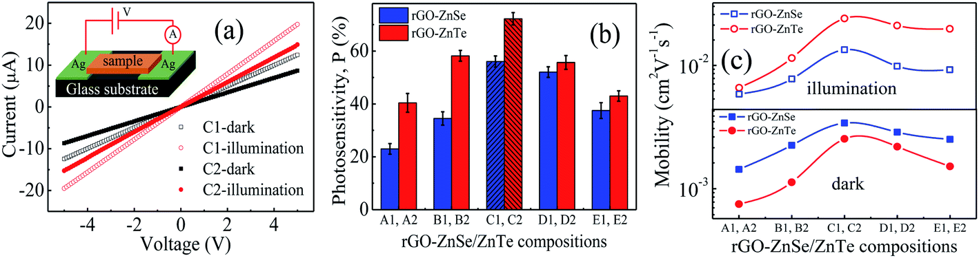 | ||
| Fig. 3 (a) I–V characteristics of C1 and C2 under dark and illumination conditions at room temperature. The inset shows the schematic diagram of samples used to measure I–V characteristics in the top electrode configuration. (b) Comparison of the photosensitivity of different rGO–ZnSe and rGO–ZnTe compositions at room temperature. Maximum responses from both the composites (C1 and C2) are shaded. (c) Comparison of the mobility values of different rGO–ZnSe and rGO–ZnTe composites at 380 K temperature. | ||
To understand the charge transport processes in the Al/semiconductor composite (active layer) junction, J–V characteristics have been measured in the 87–473 K temperature range with the top-bottom electrode configuration, as shown in Fig. 4(a), (b), and S(V) (in the ESI†) in the dark and under illumination. The current density increases under illumination at any particular temperature which implies photogeneration of charge carriers in the samples. The individual J–V curve follows J − Vm power law. The J–V characteristics consist of two distinct regions having different exponent (m) values which signify different charge transport processes. Region I (shown in the inset of Fig. 4(a)) is denoted by Ohm's law (J–V). In region II, above a certain threshold voltage, the injected carriers dominate over the intrinsic carrier concentration and we have a SCLC region with m ≥ 2.21,22,37 When there are no traps or the trap states do not take part in charge transport, the J–V characteristics may be described with the Mott–Gurney equation38
 | (1) |
 | ||
| Fig. 4 (a) J–V characteristics of sample C2 (a) in the dark and (b) under illumination at different temperatures. The inset of (a) shows the data (open symbols) at 280 K; solid lines are fitted to J – Vm in two regions. The inset of (b) shows the schematic diagram of samples in the top-bottom electrode configuration. (c) Electron mobilities of rGO, C1, and C2 both in the dark and under illumination at different temperatures. Mobility values have been calculated in the trap free SCLC region with m = (2 ± 0.25). (d) Percentage change in the mobility of different samples with an error bar. The change in μ has been estimated by taking the average of change in mobility values at the overlapped temperatures (e.g. four temperatures for C2). | ||
The individual J–V curve has been fitted in both regions for all three samples and the m values are tabulated in Table ST(III).† It is observed that in region II, m values show a decreasing trend with increase in temperature (m = 2.96 at 120 K and 1.99 at 300 K for C1 in the dark). At low temperatures, as the applied voltage reaches above the threshold value, the charge carriers can overcome the interface potential barrier easily. Some of the injected carriers fill these empty traps and rest of them participate in current conduction and we have m > 2.37,39 At higher temperatures, more number of carriers come out of the trap states to take part in transport processes. Injected carriers fill these unoccupied traps and consequently the m values decrease with increase in temperature. Although the m values decrease with increase in temperature (Table ST(III) in the ESI†), we assume that the systems are trap free in a limited temperature range (where m = 2 ± 0.25) and have applied eqn (1) for temperature dependent mobility calculations and the results are shown in Fig. 4(c).
Fig. 4(c) shows that μ increases monotonically with temperature due to available thermal energy. Owing to enhancement in the charge carrier concentration under illumination, the current for a given applied voltage increases. This leads to an increase of the slope of J vs. V2. As a result mobility increases under illumination as observed previously for rGO-based composites at room temperature.23 It is observed that under illumination the μ values have increased by ∼1.8 times for rGO, ∼2.5 times for C1, and ∼10.2 times for C2 compared to dark conditions. Also, this enhancement is almost constant with temperature. From the temperature dependent μ values we have estimated percentage change in mobility under illumination compared to dark conditions. It shows ∼56%, ∼150% enhancement of μ for rGO and C1, respectively, and almost three orders of magnitude higher for C2 (Fig. 4(d)). This way, Fig. 4(d) reflects the same trend as that shown in Fig. 3(c).
The nonlinear optical properties of rGO–ZnSe (C1) and rGO–ZnTe (C2) composites have been studied using a z-scan technique at different input pulse intensities, as shown in Fig. 5. The samples were dispersed in the DMF solvent by ultrasonic treatment. Upon excitation by a femtosecond (∼150 fs) laser pulse of 630 nm wavelength (energy ∼1.97 eV), the OA z-scan traces of the samples (Fig. 5(a) and (b)) show a transmittance valley which indicates reverse saturation absorption (RSA) behavior. The valley feature becomes prominent with increase in pulse intensities, signifying enhanced NLO properties. Pure DMF does not exhibit significant traces of NLA in the experimental pulse energies. To calculate the NLA coefficient (β), we have theoretically fitted the experimental data with the following equation29
 | (2) |
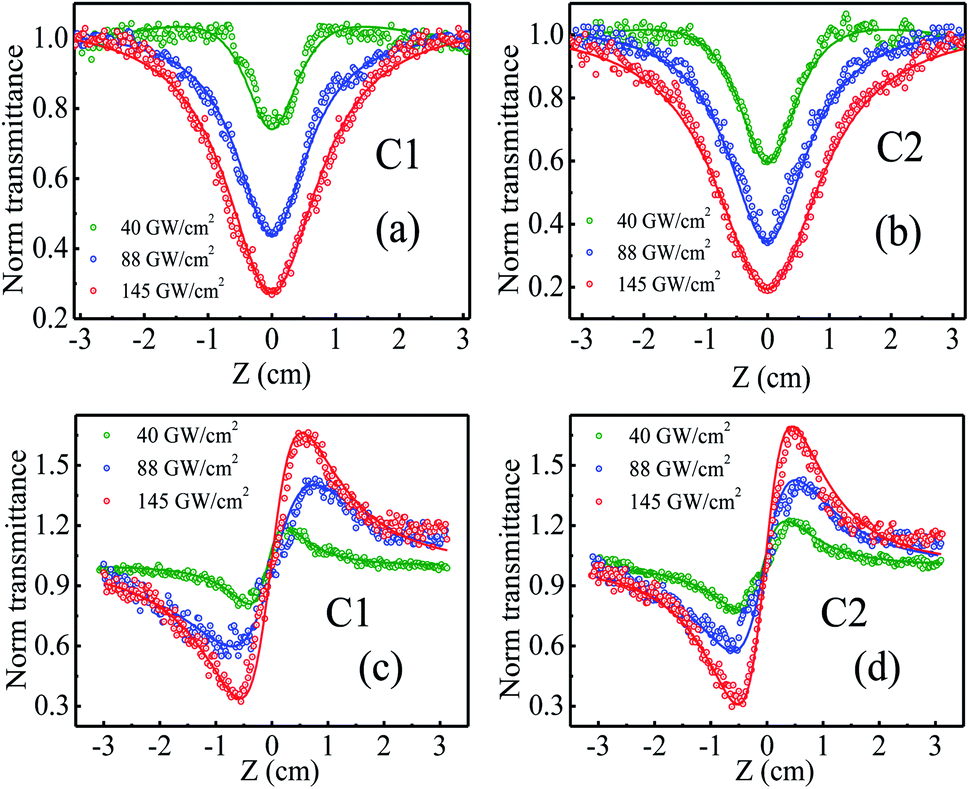 | ||
| Fig. 5 (a and b) Open aperture and (c and d) closed aperture z-scan traces of samples C1 and C2 at different input intensities. Scattered points are the experimental data and solid lines are the fitted results. | ||
 | ||
| Fig. 6 Variation of (a) NLA coefficient and (b) nonlinear refractive index of samples C1 and C2 at different input intensities. Solid lines are a guide to the eye. | ||
Fig. 5(c) and (d) show the closed aperture z-scan patterns of samples C1 and C2. CA measurements have been performed to calculate the nonlinear refractive index (n2) of the samples. The CA traces exhibit a valley-peak pattern for both the samples which points out positive n2 (self-focusing) in the measured intensity range. The n2 values have been estimated by fitting the z-scan curves with the equation given below:40
 | (3) |
The NLO behavior of rGO-based composites has been reported in the literature.26,44 For example, Anand et al. have investigated the NLO properties of hydrogen exfoliated graphene-Pd composites and reported a NLA coefficient of ∼ 4.9 × 10⁻⁴ cm GW−1 with fs excitation.44 A study has shown a β value of ∼ 1.8 × 10⁻³ cm GW−1 in exfoliated graphene-CuO hybrid composites in the fs regime.45 Saravanan et al. have reported a maximum two photon absorption coefficient of 0.1 cm GW−1 in rGO–ZnFe2O4 composites when excited with an 800 nm, 150 fs laser pulse.40 Our samples demonstrate a promising NLA coefficient (0.14–0.2 cm GW−1 for C1 and 0.22–0.3 cm GW−1 for C2) in comparison to the reports on similar systems. Besides, other layered nonlinear optical materials such as TiS2 films depict a β value of −4 × 104 cm GW−1 in the femtosecond regime.46 Ni-metal organic frameworks (MOFs) show saturation absorption behavior with β of −3 × 10⁻² cm GW−1 and n2 ∼ −8 × 10⁻⁷ cm2 GW−1.47 Antimonene possesses a giant nonlinear refractive index of ∼104 cm2 GW−1 at 532 and 633 nm continuous laser.48 Though our samples exhibit higher values of β than Ni-MOF, they depict lower NLO coefficients compared to layered antimonene and TiS2 films. The possibilities of tuning the optical nonlinearity of rGO–ZnSe and rGO–ZnTe are manifold such as by varying the fraction of oxygen functional groups present in rGO sheets, size of ZnSe/ZnTe nanoparticles, wavelength of the laser beam etc.
To reveal the applicability of the samples at low and high temperatures, photoresponse measurements have been performed at 84–460 K. Fig. S(VIII)† shows I–V characteristics of the samples under dark and illumination conditions at different temperatures. It is observed that P values decrease with increasing temperature (Fig. 7) for all the samples. At high temperatures, phonon density is comparatively higher which results in enhanced electron–phonon scattering. Also electron–electron scattering increases as temperature increases.49,50 With increase in different scattering factors, transit time (average time taken by charge carriers to travel from one electrode to the other) will be increased. This leads to a decrease in the charge collection rate at the electrode51 and consequently, photosensitivity decreases with increase in temperature. Moreover, it is observed that the P values of C1 are lower than those of sample C2. Pure ZnSe has a higher band gap (2.65 eV) compared to ZnTe (2.4 eV) (Fig. S(III)(a) and (c)†). For white light illumination with a xenon lamp, the probability of exciton dissociation in ZnTe is more as compared to that in ZnSe. Besides, the charge transfer rate between the semiconductor and rGO sheet plays an important role in determining the photosensitivity of rGO–semiconductor composites.
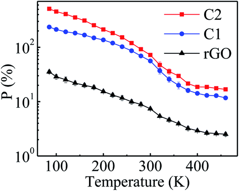 | ||
| Fig. 7 Photosensitivity of rGO, C1, and C2 at different temperatures with error bars. The error bars are evaluated from values obtained for identical samples in different measurements. Error bars are small compared to the dimension of points for some data. | ||
To find the correlation between the charge carrier mobility and defect states of the system, trap state density (Nt) has been calculated by extrapolating the J–V curves, as shown in Fig. 8(a) and (b), and S(VII).† The trap states start to get filled up with charge carriers with increasing bias voltage. After a certain voltage (VC), all the trap states are filled and this temperature independent voltage is given by52VC = qNtd2/2ε0εr. The VC values have been obtained from the extrapolated J–V curves and hence trap density is calculated under both dark and illumination conditions, as shown in Fig. 8(c). Fig. 4(c) and 8(c) indicate that charge carrier mobility is the highest for rGO under both dark and illumination conditions. The μ values are the lowest for samples C2 and C1 in the dark and under illumination, respectively. It is worth mentioning that rGO possesses minimum density of trap states irrespective of dark or illumination conditions whereas trap density is maximum for C2 (2.87 × 10²² m−3) in the dark and sample C1 (1.35 × 10²² m−3) under illumination.
 | ||
| Fig. 8 Extrapolation of J–V curves at different temperatures for C2 under (a) dark and (b) illumination conditions which gives VC ∼ 51 V and 21 V, respectively. (c) Comparison of room temperature μ and Nt values of rGO, C1 and C2 in the dark and under illumination. | ||
Generally trap states originate from structural disorder and surface defects that are exponentially distributed within the energy band gap.53 When graphite powder is oxidized to GO or during the reduction of GO to rGO, part of the C–C network gets distorted in the processes creating vacancies, defects etc.54 Moreover, the folding and wrinkling of rGO sheets create defects.55 The trap states are regarded as the degree of disorderness which restrains the movement of charge carriers in a sample. So the lowest trap density in rGO under both dark and illumination conditions correlates well to the fact that among three samples, rGO has the best charge carrier mobility values. Similarly, trap density in samples C1 and C2 follows an opposite trend of carrier mobility for both dark and illumination conditions (Fig. 8(c)).
The intensified light–matter interplay between the rGO–nanoparticle composite and white light/fs laser can be interpreted with the help of PL quenching (Fig. S(III)(b) and (d) in the ESI†). The efficient fluorescence quenching of rGO–ZnSe/rGO–ZnTe appears due to photoinduced electron transfer from the nanoparticle to graphene sheets. Absorbed photons create excitons within ZnSe/ZnTe which in effect dissociate at the ZnSe/ZnTe–rGO interface and then get transferred to the electrodes through the rGO matrix by means of excellent electron accepting nature of the latter.16 To get further insight about electronic interactions between rGO sheets and nanoparticles, time resolved fluorescence decays of samples C1 and C2 were measured at 304 nm excitation wavelength, shown in Fig. 9. The decay curves are fitted biexponentially and the corresponding decay times are tabulated in Table 1. The fast decaying component (τ1) corresponds to electron transfer from the conduction band of the nanoparticle to rGO and the second term (τ2) is due to electron transition from an intermediate defect state to the valence band of the nanoparticle.56,57 Interestingly, from Table 1 it is observed that the fast component for C1 is twice as much as that for C2 (0.50 ns vs. 0.26 ns) whereas the slow time scale is comparable for both. The decrease in the fast component signifies a better transfer rate of photogenerated electrons to rGO in C2.
 | ||
| Fig. 9 Time resolved decay curves of C1 and C2. The inset shows the enlarged view of the decay curves. | ||
| Sample | τ 1 (ns) (a1) | τ 2 (ns) (a2) |
|---|---|---|
| rGO–ZnSe (C1) | 0.50 (0.65) | 7.60 (0.35) |
| rGO–ZnTe (C2) | 0.26 (0.80) | 7.80 (0.20) |
So far we have observed that the dark mobility of rGO–ZnSe is more compared to rGO–ZnTe. But under illumination (white light or femtosecond laser pulse) rGO–ZnTe shows better optoelectronic properties than rGO–ZnSe. While dark mobility for a composite system depends primarily on the disorderness of the matrix, TCSPC studies give us a hint that the improved optoelectronic properties of rGO–ZnTe could be due to better and efficient charge transfer between graphene sheets and nanoparticles. It is then logical to compare the disorderness between rGO–ZnSe and rGO–ZnTe composites. A comparison may be achieved from frequency dependent conductivity measurements as described in our previous article. The exponent (s) value of Jonscher's power law (σ(ω) ∼ Bωs,58 where σ represents the conductivity, B is a prefactor, and ω stands for angular frequency) is a measure of disorder. In general, the higher value of s signifies higher disorder in a system.58,59 We have measured s ∼ 1.3 for rGO–ZnTe16 whereas in the case of the rGO–ZnSe composite, it is ∼0.96 at room temperature (see Fig. S(IX) and subsequent discussion in the ESI†). These values point to more disordered nature of the rGO–ZnTe system than rGO–ZnSe, and we observe less mobile charge carriers under dark conditions in the former matrix (Fig. 4(c)). Under illumination the fast transfer of photogenerated carriers plays an important role and rGO–ZnTe performs better in terms of photosensitivity, NLO properties, and μ values under illumination than rGO–ZnSe. At the microscopic level, better and uniform dispersion of ZnTe nanoparticles on rGO sheets as compared to ZnSe nanoparticles is evident from the TEM images (Fig. 2). Better dispersion of ZnTe nanoparticles leads to better surface sharing, i.e. electronic coupling between ZnTe and rGO sheets, resulting in two fold faster charge transfer compared to the rGO–ZnSe system (Table 1).
4 Conclusions
In summary, photosensitive hybrid composites based on rGO–ZnSe and rGO–ZnTe with different compositions have been synthesized. Photosensitivity and charge carrier mobility measurements on different compositions reveal that samples C1 and C2 are the most efficient optoelectronic materials. Temperature dependent P values indicate a decreasing trend for rGO, C1, and C2 with increasing temperature owing to the enhanced charge carrier scattering mechanisms. Comparative study on change in μ (dark to illumination) and P of these two samples indicates a better performance of C2 in the entire temperature range. Moreover, the measured NLA coefficient and n2 values in the femtosecond regime of sample C2 are higher than C1. Our samples demonstrate better third order optical nonlinearity as compared to other rGO-based composites. The better optoelectronic performances of C2 can be attributed to the faster photoinduced charge transfer rate and better dispersion of ZnTe nanoparticles on rGO sheets, which would provide a platform for manifold optoelectronic applications of the rGO–ZnTe hybrid system.Conflicts of interest
There are no conflicts to declare.Acknowledgements
DST FIST funded XPS facility at the Department of Physics, IIT Kharagpur is thankfully acknowledged. The authors are grateful to the SDGRI scheme (UPM project) of IIT Kharagpur for the z-scan measurement facility. We thank Prof. Nilmoni Sarkar's group (Department of Chemistry, IIT Kharagpur) for TCSPC measurements.References
- K. S. Novoselov, A. K. Geim, S. V. Morozov, D. Jiang, M. I. Katsnelson, I. V. Grigorieva, S. V. Dubonos and A. A. Firsov, Two-dimensional gas of massless dirac fermions in graphene, Nature, 2005, 438, 197–200 CrossRef CAS PubMed.
- A. K. Geim, Graphene: status and prospects, Science, 2009, 324, 1530–1534 CrossRef CAS PubMed.
- J.-H. Chen, C. Jang, S. Xiao, I. Masa and M. S. Fuhre, Intrinsic and extrinsic performance limits of graphene devices on sio2, Nat. Nanotechnol., 2008, 3, 206–209 CrossRef CAS PubMed.
- M. Freitag, Graphene: nanoelectronics goes flat out, Nat. Nanotechnol., 2008, 3, 455–457 CrossRef CAS PubMed.
- R. Balog, B. Jørgensen, L. Nilsson, M. Andersen, E. Rienks, M. Bianchi, M. Fanetti, E. Lægsgaard, A. Baraldi, S. Lizzit, Z. Sljivancanin, F. Besenbacher, B. Hammer, T. G. Pedersen, P. Hofmann and L. Hornekær, Bandgap opening in graphene induced by patterned hydrogen adsorption, Nat. Mater., 2010, 9, 315–319 CrossRef CAS PubMed.
- H. He, J. Klinowski, M. Forster and A. Lerf, A new structural model for graphite oxide, Chem. Phys. Lett., 1998, 287, 53–56 CrossRef CAS.
- D. Joung and Saiful I. Khondaker, Efros-shklovskii variable-range hopping in reduced graphene oxide sheets of varying carbon sp2 fraction, Phys. Rev. B, 2012, 86(1–8), 235423 CrossRef.
- S. Pei and H.-M. Cheng, The reduction of graphene oxide, Carbon, 2012, 50, 3210–3228 CrossRef CAS.
- C. Berger, Z. Song, X. Li, X. Wu, N. Brown, C. Naud, D. Mayou, T. Li, J. Hass, A. N. Marchenkov, E. H. Conrad, P. N. First and W. A. de Heer, Electronic confinement and coherence in patterned epitaxial graphene, Science, 2006, 312, 1191–1196 CrossRef CAS PubMed.
- I. Jung, D. A. Dikin, R. D. Piner and R. S. Ruoff, Tunable electrical conductivity of individual graphene oxide sheets reduced at “low” temperatures, Nano Lett., 2008, 8, 4283–4287 CrossRef CAS PubMed.
- G. Scott, S. Han, M. Wang, K. L. Wang and R. B. Kaner, A chemical route to graphene for device applications, Nano Lett., 2007, 7, 3394–3398 CrossRef PubMed.
- D. Li, M. B. Müller, G. Scott, R. B. Kaner and G. G. Wallace, Processable aqueous dispersions of graphene nanosheets, Nat. Nanotechnol., 2008, 3, 101–105 CrossRef CAS PubMed.
- L. Yang, J. Zhu and D. Xiao, Microemulsion-mediated hydrothermal synthesis of ZnSe and Fe-doped ZnSe quantum dots with different luminescence characteristics, RSC Adv., 2012, 2, 8179–8188 RSC.
- K. Chakraborty, T. Pal and S. Ghosh, rGO-ZnTe: a graphene based composite for tetracycline degradation and their synergistic effect, ACS Appl. Nano Mater., 2018, 1, 3137–3144 CrossRef CAS.
- X.-P. Wu, J. Gu, S.-M. Zhou, X.-Y. Li, S.-L. Wang, L. Jin, H. Chen and J.-J. Shi, Red bayberry-like ZnTe microstructures: controlled synthesis, growth mechanism and enhanced photocatalytic performance, J. Alloys Compd., 2015, 627, 166–173 CrossRef CAS.
- A. Sarkar, A. B. Rahaman, K. Chakraborty, T. Pal, S. Ghosh and D. Banerjee, ZnTe dispersed in rGO matrix: investigation of electrical transport processes, magnetic properties and their synergistic effect, Appl. Surf. Sci., 2019, 493, 279–286 CrossRef CAS.
- S. Chakrabarty, K. Chakraborty, A. Laha, T. Pal and S. Ghosh, Photocurrent generation and conductivity relaxation in reduced graphene oxide Cd0.75Zn0.25S nanocomposite and its photocatalytic activity, J. Phys. Chem. C, 2014, 118, 28283–28290 CrossRef CAS.
- K. Chakraborty, S. Chakrabarty, T. Pal and S. Ghosh, Synergistic effect of zinc selenide–reduced graphene oxide towards enhanced solar light-responsive photocurrent generation and photocatalytic 4-nitrophenol degradation, New J. Chem., 2017, 41, 4662–4671 RSC.
- C. Yim, N. McEvoy, H.-Y. Kim, E. Rezvani and G. S. Duesberg, Investigation of the interfaces in schottky diodes using equivalent circuit models, ACS Appl. Mater. Interfaces, 2013, 5, 6951–6958 CrossRef CAS PubMed.
- Z. Chiguvare and V. Dyakono, Trap-limited hole mobility in semiconducting poly(3-hexylthiophene), Phys. Rev. B, 2004, 70(1–8), 235207 CrossRef.
- Y.-H. Lou, L. Zhang, M.-F. Xu, Z.-K. Wang, S. Naka, H. Okada and L.-S. Liao, Direct comparison of charge transport and electronic traps in polymer–fullerene blends under dark and illuminated conditions, Org. Electron., 2014, 15, 299–305 CrossRef CAS.
- D. Joung, A. Chunder, L. Zhai and S. I. Khondaker, Space charge limited conduction with exponential trap distribution in reduced graphene oxide sheets, Appl. Phys. Lett., 2010, 97(1–3), 093105 CrossRef.
- M. Das, J. Datta, R. Jana, S. Sil, S. Halder and P. P. Ray, Synthesis of rGO–Zn0.8Cd0.2S via in situ reduction of go for the realization of a schottky diode with low barrier height and highly enhanced photoresponsivity, New J. Chem., 2017, 41, 5476–5486 RSC.
- S. M. Sze, Physics of Semiconductor Devices, John Wiley and Sons, 1981 Search PubMed.
- X. Zhao, Z.-B. Liu, W.-B. Yan, Y. Wu, X.-L. Zhang, Y. Chen and J.-G. Tian, Ultrafast carrier dynamics and saturable absorption of solution processable few-layered graphene oxide, Appl. Phys. Lett., 121905, 98(1–3), 2011 Search PubMed.
- S. Bhattacharya, C. Biswas, S. S. K. Raavi, J. V. S. Krishna, N. V. Krishna, L. Giribabu and V. Rao Soma, Synthesis, optical, electrochemical, dft studies, nlo properties, and ultrafast excited state dynamics of carbazole-induced phthalocyanine derivatives, J. Phys. Chem. C, 2019, 123, 11118–11133 CrossRef CAS.
- A. B. Rahaman, S. Bhattacharya, A. Sarkar, T. Singha, D. Banerjee and P. K. Datta, Enhancement of ultrafast nonlinear optical response of zinc selenide nanoparticle decorated reduced graphene oxide sheets, J. Appl. Phys., 2019, 126(1–10), 233101 CrossRef.
- E. Garmire, Nonlinear optics in daily life, Opt. Express, 2013, 21, 30532–30544 CrossRef PubMed.
- S. Bhattacharya, R. Maiti, A. C. Das, S. Saha, S. Mondal, S. K. Ray, S. N. B. Bhaktha and P. K. Datta, Efficient control of ultrafast optical nonlinearity of reduced graphene oxide by infrared reduction, J. Appl. Phys., 2016, 120(1–8), 013101 CrossRef.
- A. Wang, Yu Wang, Yu Fang, Y. Song, J. Ding, L. Long, M. P. Cifuentes, M. G. Humphrey and C. Zhang, Facile hydrothermal synthesis and optical limiting properties of TiO2-reduced graphene oxide nanocomposites, Carbon, 2015, 89, 130–141 CrossRef CAS.
- W. S. Hummers Jr and R. E. Offema, Preparation of graphitic oxide, J. Am. Chem. Soc., 1958, 80, 1339 CrossRef.
- A. B. Rahaman, A. Sarkar, K. Chakraborty, J. Mukherjee, T. Pal, S. Ghosh and D. Banerjee, Observation of different charge transport processes and origin of magnetism in rGO and rGO-ZnSe composite, J. Phys. Chem. C, 2019, 123, 15441–15450 CrossRef CAS.
- L. Stobinski, B. Lesiak, A. Malolepszy, M. Mazurkiewicz, B. Mierzwa, J. Zemek, P. Jiricek and I. Bieloshapka, Graphene oxide and reduced graphene oxide studied by the XRD, TEM and electron spectroscopy methods, J. Electron Spectrosc. Relat. Phenom., 2014, 195, 145–154 CrossRef CAS.
- S. Sarkar, S. Acharya, A. Chakraborty and N. Pradhan, Zinc blende 0d quantum dots to wurtzite 1d quantum wires: the oriented attachment and phase change in ZnSe nanostructures, J. Phys. Chem. Lett., 2013, 4, 3292–3297 CrossRef CAS.
- M. Fahad Ehsan, M. Naeem Ashiq and He Tao, Hollow and mesoporous ZnTe microspheres: synthesis and visible-light photocatalytic reduction of carbon dioxide into methane, RSC Adv., 2015, 5, 6186–6194 RSC.
- Y. L. Cao, Y. B. Tang, Y. Liu, Z. T. Liu, L. B. Luo, Z. B. He, J. S. Jie, R. Vellaisamy, W. J. Zhang, C. S. Lee and S. T. Lee, Coaxial nanocables of p–type zinc telluride nanowires sheathed with silicon oxide: synthesis, characterization and properties, Nanotechnology, 2009, 20(1–7), 455702 CrossRef CAS PubMed.
- A. Sarkar, A. B. Rahaman and D. Banerjee, Temperature dependent charge transport studies across thermodynamic glass transition in P3HT:PCBM bulk heterojunction: insight from J–V and impedance spectroscopy, J. Phys. D: Appl. Phys., 2018, 51(1–10), 095602 CrossRef.
- M. A. Lampert and P. Mark, Current Injection in Solids, Academic Press, New York, 1970 Search PubMed.
- A. B. Rahaman, D. Giri, A. Sarkar, S. K. Patra and D. Banerjee, Effect of thermodynamic glass transition on charge transport properties in a benzodithieno-imidazole π-conjugated polymer: fullerene blend, Mater. Res. Express, 2019, 6(1–8), 115114 CrossRef.
- M. Saravanan, T. C. Sabari Girisun, G. Vinitha and S. Venugopal Rao, Improved third-order optical nonlinearity and optical limiting behaviour of (nanospindle and nanosphere) zinc ferrite decorated reduced graphene oxide under continuous and ultrafast laser excitation, RSC Adv., 2016, 6, 91083–91092 RSC.
- K. Wang, J. Wang, J. Fan, M. Lotya, A. O'Neill, D. Fox, Y. Feng, X. Zhang, B. Jiang, Q. Zhao, H. Zhang, J. N. Coleman, L. Zhang and W. J. Blau, Ultrafast saturable absorption of two-dimensional MoS2 nanosheets, ACS Nano, 2013, 7, 9260–9267 CrossRef CAS PubMed.
- R. A. Ganeev, I. A. Kulagin, A. I. Ryasnyansky, R. I. Tugushev and T. Usmanov, Characterization of nonlinear optical parameters of KDP, LiNbO3 and BBO crystals, Opt. Commun., 2004, 229, 403–412 CrossRef CAS.
- D. Wang, T. Li, S. Wang, J. Wang, Z. Wang, X. Xu and F. Zhang, Study on nonlinear refractive properties of KDP and DKDP crystals, RSC Adv., 2016, 6, 14490–14495 RSC.
- B. Anand, A. Kaniyoor, S. Siva Sankara Sai, R. Philip and S. Ramaprabhu, Enhanced optical limiting in functionalized hydrogen exfoliated graphene and its metal hybrids, J. Mater. Chem. C, 2013, 1, 2773–2780 RSC.
- B. Anand, A. Kaniyoor, D. Swain, T. T. Baby, S. Venugopal Rao, S. Siva Sankara Sai, S. Ramaprabhu and R. Philip, Enhanced optical limiting and carrier dynamics in metal oxide-hydrogen exfoliated graphene hybrids, J. Mater. Chem. C, 2014, 2, 10116–10123 RSC.
- Y. Ge, Z. Zhu, Y. Xu, Y. Chen, S. Chen, Z. Liang, Y. Song, Y. Zou, H. Zeng, S. Xu, H. Zhang and D. Fan, Broadband nonlinear photoresponse of 2d TiS2 for ultrashort pulse generation and all-optical thresholding devices, Adv. Opt. Mater., 2018, 6(1–10), 1701166 CrossRef.
- X. Jiang, L. Zhang, S. Liu, Y. Zhang, Z. He, W. Li, F. Zhang, Y. Shi, L. ü Wei, Li Yu, W. Qiao, J. Li, J. Feng, S. Ruan, Yu-J. Zeng, Xi Zhu, Y. Lu and H. Zhang, Ultrathin metal–organic framework: An emerging broadband nonlinear optical material for ultrafast photonics, Adv. Opt. Mater., 2018, 6(1–11), 1800561 CrossRef.
- L. Lu, X. Tang, R. Cao, L. Wu, Z. Li, G. Jing, B. Dong, S. Lu, Y. Li, Y. Xiang, J. Li, D. Fan and H. Zhang, Broadband nonlinear optical response in few-layer antimonene and antimonene quantum dots: a promising optical kerr media with enhanced stability, Adv. Opt. Mater., 2017, 5(1–9), 1700301 CrossRef.
- Abid, P. Sehrawat, S. S. Islam, P. Mishra and S. Ahmad, Reduced graphene oxide (rGO) based wideband optical sensor and the role of temperature, defect states and quantum efficiency, Sci. Rep., 2018, 8(1–12), 3537 CrossRef CAS PubMed.
- P. Sehrawat, Abid, S. S. Islam and P. Mishra, Reduced graphene oxide based temperature sensor: Extraordinary performance governed by lattice dynamics assisted carrier transport, Sens. Actuators, B, 2018, 258, 424–435 CrossRef CAS.
- B. G. Streetman and S. K. Banerjee, Solid State Electronic Devices, Prentice-Hall, 2005 Search PubMed.
- V. Kumar, S. C. Jain, A. K. Kapoor, J. Poortmans and R. Mertens, Trap density in conducting organic semiconductors determined from temperature dependence of J–V characteristics, J. Appl. Phys., 2003, 94, 1283–1285 CrossRef CAS.
- S. Baidyaroy and P. Mark, Analytical and experimental investigation of the effects of oxygen chemisorption on the electrical conductivity of cds, Surf. Sci., 1972, 30, 53–68 CrossRef CAS.
- W. Zhang, V. Carravetta, Z. Li, Y. Luo and J. Yang, Oxidation states of graphene: insights from computational spectroscopy, J. Chem. Phys., 2009, 131(1–6), 244505 CrossRef PubMed.
- H. C. Schniepp, Je-L. Li, M. J. McAllister, H. Sai, M. Herrera-Alonso, D. H. Adamson, R. K. Prud’homme, R. Car, D. A. Saville and I. A. Aksay, Functionalized single graphene sheets derived from splitting graphite oxide, J. Phys. Chem. B, 2006, 110, 8535–8539 CrossRef CAS PubMed.
- S. Maity, D. Bain, K. Bhattacharyya, S. Das, R. Bera, B. Jana, B. Paramanik, A. Datta and A. Patra, Ultrafast relaxation dynamics of luminescent copper nanoclusters (Cu7L3) and efficient electron transfer to functionalized reduced graphene oxide, J. Phys. Chem. C, 2018, 122, 13354–13362 CrossRef CAS.
- Z. S. Seddigi, S. A. Ahmed, S. Sardar and S. K. Pal, Ultrafast dynamics at the zinc phthalocyanine/zinc oxide nanohybrid interface for efficient solar light harvesting in the near red region, Sol. Energy Mater. Sol. Cell., 2015, 143, 63–71 CrossRef CAS.
- S. R. Elliot, AC conduction in amorphous chalcogenide and pnictide semiconductors, Adv. Phys., 1987, 36, 135–218 CrossRef.
- J. Parui and S. B. Krupanidhi, Slim p-e hysteresis loop and anomalous dielectric response in sol-gel derived antiferroelectric pbzro3 thin films, J. Appl. Phys., 2008, 104(1–11), 024107 CrossRef.
Footnotes |
| † Electronic supplementary information (ESI) available: XPS full surface survey spectrum, SEM images, UV-vis absorption and PL spectra, J–V characteristics, capacitance–frequency response, sample thickness, the dielectric constant, values of m in the dark and under illumination, and the frequency dependent conductivity of samples C1 and C2. See DOI: 10.1039/c9na00728h |
| ‡ These authors contributed equally to this work. |
| § Present address: Department of Physics, Uluberia College, Uluberia, 711315, India. |
| This journal is © The Royal Society of Chemistry 2020 |