
 Open Access Article
 This Open Access Article is licensed under a Creative Commons Attribution-Non Commercial 3.0 Unported Licence
A novel strategy to design a multilayer functionalized Cu2S thin film counter electrode with enhanced catalytic activity and stability for quantum dot sensitized solar cells†
Libin
Wu
a,
Zhengmeng
Lin
a,
Pengyu
Feng
a,
Liping
Luo
a,
Lanlan
Zhai
 *a,
Fantai
Kong
b,
Yun
Yang
a,
Lijie
Zhang
a,
Shaoming
Huang
*c and
Chao
Zou
*a
*a,
Fantai
Kong
b,
Yun
Yang
a,
Lijie
Zhang
a,
Shaoming
Huang
*c and
Chao
Zou
*a
aZhejiang Key Laboratory of Carbon Materials, College of Chemistry and Material Engineering, Wenzhou University, Wenzhou 325027, People's Republic of China. E-mail: zhaill@wzu.edu.cn; zouchao@wzu.ed.cn
bKey Laboratory of Photovoltaic and Energy Conservation Materials, Institute of Applied Technology, Hefei Institutes of Physical Science, Chinese Academy of Sciences, Hefei 230088, People's Republic of China
cSchool of Materials and Energy, Guangdong University of Technology, Guangzhou 510006, People's Republic of China. E-mail: smhuang@gdut.edu.cn
First published on 6th January 2020
Abstract
As the essential component of a quantum dot-sensitized solar cell (QDSC), the counter electrode (CE) plays an important role in electron transfer and catalytic reduction acquisition throughout the device. A novel route to design multilayer functionalized Cu2S thin films as CEs with high catalytic activity and enhanced stability, as well as large specific surface area and high conductivity, is presented. Firstly, Mo-based films were prepared by magnetron sputtering on a glass substrate, and then porous CuZnMo conductive films were formed by etching with hydrochloric acid. Secondly, indium tin oxide (ITO) film was sputtered onto the porous structure to act as a protective layer, and a porous ITO/CuZnMo structured film was obtained after optimization. In the third step, multilayer Cu(x)/ITO/CuZnMo structured films were acquired by sputtering Cu films. Finally, multilayer Cu2S(t)/ITO/CuZnMo functionalized film CEs were obtained via in situ sulfidation of sputtered Cu films. The functions of conduction and resistance to electrolyte corrosion were produced and enhanced by annealing an ITO layer at high temperature prior to Cu deposition, while catalytic activity enabled by Cu2S was realized from Cu film sulfidation. The multilayer Cu2S/ITO(500 °C)/CuZnMo functionalized films exhibit high catalytic activity and enhanced stability for resistance to electrolyte corrosion. Taking multilayer Cu2S/ITO(500 °C)/CuZnMo films as CEs, the QDSCs demonstrated good stability of power conversion efficiency (PCE) after 500 h of irradiation, from an initial 4.21% to a final 4.00%. Furthermore, the thickness of Cu2S film modulated by the duration of Cu sputtering was investigated. It was found that the QDSCs using multilayer Cu2S(40 min)/ITO/CuZnMo functionalized film with a Cu2S thickness of 1.2 μm as CE exhibit the best performance, and the Rct value was 0.57 Ω. The best photovoltaic performance with a PCE of 5.21% (Voc = 533.1 mV, Jsc = 18.80 mA cm−2, FF = 52.84%) was achieved under AM 1.5 radiation with an incident power of 100 mW cm−2. This design of a multilayer functionalized CE introduces potential alternatives to the common brass-based CE for long-term QDSCs with high performance.
1 Introduction
As third-generation solar photovoltaic devices, semiconductor quantum dot-sensitized solar cells (QDSCs) have received a great deal of attention in recent years.1–3 Semiconductor quantum dots (QDs) as sensitizers are considered to be the best alternatives for the dye in dye-sensitized solar cells,4 and have many excellent properties, including multiple exciton effect, band-gap energy controllability, high absorption coefficient, simple preparation method and quantum confinement effect.5–7 Moreover, the theoretical power conversion efficiency (PCE) of QDSCs has been predicted to be 44%, which breaks the Shockley–Queisser limit (31%).8–10QDSCs consist mainly of photoanode adsorbing QDs, electrolyte and CE. QD sensitizers11,12 are commonly binary, ternary, or quaternary semiconductors, such as CdS,13,14 CdSe,15 PbS,16,17 Ag2Se,18 ZnS,19 AgInSe2,20 CuIn(S,Se)2,21 or Cu2ZnSnS4 (CZTS).22 To improve the performance of QDSCs, one should not only consider the influence of QDs on the performance, but also the required properties of the CE and electrolyte. The electrolyte is used as a material for electron and hole transport in QDSCs.23 Organic electrolytes with I3−/I− redox couples have been widely used as electrolytes in DSSCs. However, I3−/I− redox couples can easily corrode QDs, forming cadmium iodide, leading to a deterioration in QDSC performance.24,25 Thus, QDSCs mainly use polysulfide electrolyte S2−/S22− as an electrolyte which can provide a stable environment for QDs.26 Pt-based CEs have been widely used as electrolytes in DSSCs due to their high catalytic ability with I3−/I− redox couples.27 However, Pt-based CEs can adsorb sulfur atoms, leading to a decrease in surface activity and conductivity of CEs.28,29 In recent years, a variety of CEs has been used on QDSCs to substitute for Pt-based CEs, such as metal electrodes, metal chalcogenides, polymers, or composite CEs. Chalcogenides have been applied to CEs with high-conductivity catalytic activity for polysulfide electrolytes.29–33
As a catalytic reduction regeneration medium for electron transport and the realization of an electrolyte redox couple in QDSCs, CEs are mainly composed of a conductive substrate and a catalytic material.34,35 Therefore, an excellent CE should have the following merits: (1) good electrical conductivity; (2) high catalytic activity; (3) a large specific surface area to provide more active sites for the electrolyte; (4) corrosion resistance to the electrolyte. Like the photoanode, there are many materials which can be selected as a conductive substrate material, such as metal, FTO conductive glass, ITO-PET, ITO-PEN, etc.36–38 Currently, the commonest CE for QDSCs is the traditional brass-based CE.39–41 The brass-based CE is made by hydrochloric acid etching of the active metal, forming a porous construction, and then polysulfide electrolyte being added to form a compact Cu2S film.42 However, the polysulfide electrolyte continues to corrode the CuZn alloy, resulting in unstable performance of the QDSCs. In order to improve the corrosion resistance of the substrate material, researchers have used a non-metallic material as a conductive substrate material. Wang et al. coated Cu2S films on FTO glass with DMSO as a template by an electroplating method to achieve an efficiency of 4.32% of QDSCs.43 Zhong et al. used a highly conductive titanium mesh as the conductive substrate, coated with a layer of activated mesoporous carbon (MC/Ti) to improve conductivity and catalytic performance. They found that the performance of QDSCs was greatly improved with PCE = 11%.44 Prabakar et al. coated an FTO layer onto glass by a screen-printing method, and prepared hexagonal CuS film by chemical bath deposition to achieve a better performance.32 Meng et al. deposited a thin copper layer on the surface of FTO by an electroplating method, and then immersed the copper layer coated glass in polysulfide solution to form a Cu2S CE. The favourable porous structure of the film promoted better catalytic ability, and QDSCs assembled with the CE and CdS QD based photoanode exhibited a PCE of 2.6%.45 Wang et al. prepared nanosheet-structured CuxS thin films as CEs, and the corresponding CdS/CdSe QDSC achieved the best PCE of 3.67%.46 However, suffering from continuous sulfidation by polysulfide electrolyte, the aforementioned CEs, including brass/Cu2S, CuS/FTO, and MC/Ti, have shortcomings, such as poor stability, low resistance under pressure, and easy detachment from the Ti mesh. Therefore, it still remains a challenge to find a suitable CE with high conductivity and resistance to electrolyte corrosion.
In response to these challenges, herein we provide a route to design functionalized CEs achieving a large specific surface area arising from the porous structures of an etched alloy layer, improved conductivity and resistance to electrolyte corrosion originating from an annealed ITO layer, and high catalytic activity provided by cuprous sulfide. The design adopts a four-step process method. Firstly, Mo-based films were prepared by magnetron sputtering, and then porous CuZnMo conductive films were obtained by hydrochloric acid etching. Secondly, a layer of ITO film was sputtered onto the porous structure as a protective film, and a porous ITO/CuZnMo structured film was prepared after optimization. Thirdly, multilayer Cu(x)/ITO/CuZnMo structured films were sputtered with different thicknesses of Cu films. Finally, multilayer Cu2S(t)/ITO/CuZnMo functionalized film CEs were obtained via one-step in situ sulfidation of Cu films. A schematic description of the preparation process is presented in Fig. 1. The annealing of the ITO/glass films at 500 °C reduced electrical resistivity from 1.06 × 10⁻² Ω cm to 2.28 × 10⁻⁴ Ω cm. The multilayer Cu2S/ITO(500 °C)/CuZnMo functionalized films used as CEs exhibited high catalytic activity and enhanced resistance to electrolyte corrosion, in which fabricated QDSCs demonstrated a stable PCE after 500 h of irradiation, from an initial 4.21% to a final 4.00%. The multilayer Cu2S(40 min)/ITO/CuZnMo functionalized film exhibited the best performance with a Cu2S thickness of 1.2 μm, and an Rct value of 0.57 Ω. The best photovoltaic performance of the QDSCs was achieved with a PCE of 5.21% (Voc = 533.1 mV, Jsc = 18.80 mA cm−2, FF = 52.84%) under AM 1.5 radiation with an incident power of 100 mW cm−2.
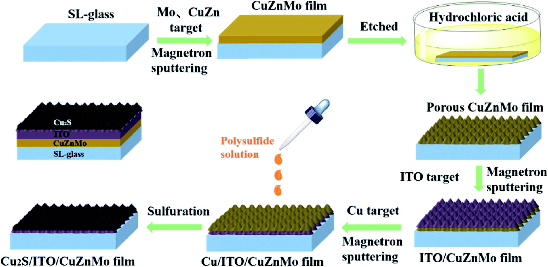 | ||
| Fig. 1 Schematic diagram for preparing multilayer Cu2S(t)/ITO/CuZnMo functionalized film CEs. | ||
2 Experimental
2.1 Materials
All chemicals were used as received without further purification. Mo target (¢ 50.8 × 5 mm, >99%), CuZn target (¢ 50.8 × 5 mm, >99.99%), ITO target (¢ 50.8 × 4 mm, >99.99%), Cu target (¢ 50 × 5 mm, >99.995%) were purchased from ZhongNuoXinCai company (Beijing, China). Copper diethyldithiocarbate (Cu(dedc)2, >97%) and indium nitrate (In(NO3)3, 99.9%) were obtained from Alfa Aesar; sodium diethyldithio-carbamate trihydrate (Na(dedc), 99%), n-hexane (95%) and 3-mercaptopropionic acid (MPA, 99%) were obtained from J&K; oleylamine (OLA, >80%) was obtained from Acros.2.2 Preparation of porous CuZnMo conductive films
Soda lime (SL) glass was cleaned in ethanol and acetone solution using an ultrasound bath for 30 min, and rinsed with ethanol and deionized water, and blow dried with nitrogen. Magnetron sputtering was used to pre-sputter Mo for 30 min on SL-glass at an Ar pressure of 1.0 Pa and power of 100 W. The Mo target was sputtered for 30 min at low pressure and high temperature, and then the Mo and CuZn alloy targets were co-sputtered for 30 min. Finally, the CuZn alloy target was sputtered for 1–1.5 h at 0.35 Pa and 100 W to obtain CuZnMo conductive film. Then, the CuZnMo conductive film was etched in concentrated hydrochloric acid for 5–10 min, rinsed with deionized water and ethanol, and blown dry with nitrogen to obtain a porous CuZnMo conductive film.2.3 Preparation of porous ITO/CuZnMo structured films and ITO/glass films
Due to the fact that the porous CuZnMo conductive film obtained after acid etching has poor corrosion resistance to the electrolyte, the film falls off easily and the surface metal is easily oxidized when it is exposed to air for a long time. To avoid this, an additional protective layer must be added onto the porous conductive film. Lower contact resistance between the applied protective layer and the porous conductive film would be better for electron transportation. In consideration of these requirements, ITO film was selected as the protective layer. ITO film was prepared by magnetron sputtering. The effects of gas atmosphere, coating time and substrate temperature on the resistivity of ITO film were optimized. Suitable conditions can be listed as follows: room temperature, Ar pressure of 0.20 Pa and power of 100 W. The films coated on SL-glass and on the porous CuZnMo conductive film were solely annealed at 200 °C, 300 °C, 400 °C, 500 °C for 2 h, and were respectively named ITO/glass-(T) films and ITO(T)/CuZnMo structured films.2.4 Preparation of Cu2S/ITO(T)/CuZnMo CEs, Cu(t)/ITO/CuZnMo films, Cu2S(t)/ITO/CuZnMo CEs and brass-based CEs
2.5 Preparation of CuInS2 QD and TiO2 photoanodes
The In(dedc)3 precursors were synthesized using a previously reported method.48,49 Briefly, Na(dedc) (6 mmol) and In(NO3)3 (2 mmol) were dissolved in 100 mL and 50 mL of deionized water, respectively. The In(NO3)3 solution was added dropwise to the Na(dedc) solution under magnetic stirring, forming a white precipitate. The precipitation was washed 3 times with ethanol and treated in a vacuum drying oven at 60 °C for 3 h. The synthesized precursors were stored in a desiccator at room temperature.For the typical synthesis of CuInS2 QDs, Cu(dedc)2 (0.5 mmol) and In(dedc)3 (0.1 mmol) were loaded into a 50 mL round-bottom flask, followed by the addition of 4 mL of oleylamine. The above mixture was treated ultrasonically and was then heated in a 180 °C oil bath for 1 h. When the reaction was complete, the solution was cooled to room temperature. The dark red product was collected via centrifugation and washed several times with absolute ethanol and n-hexane. The obtained CuInS2 QDs were dispersed in dichloromethane.
Ligand exchange of oil-soluble CuInS2 QDs to water-soluble QDs can improve adsorption performance. For a typical ligand exchange, 130 μL of MPA was dissolved in 1 mL of methanol, and then the pH was adjusted to about 9 using 30% NaOH solution. The MPA solution was slowly added into 15 mL of CuInS2 QD solution under magnetic stirring. After 30 min, water-soluble CuInS2 QDs precipitated; then 10 mL of deionized water was added and the mixture was stirred for another 30 min. The aqueous phase containing the MPA-capped CuInS2 QDs was collected. The aqueous dispersion was further purified by centrifugation and decantation with the addition of acetone. The precipitation was redissolved in 1.0 mL of deionized water.
The double-layered mesoporous TiO2 photoanodes were fabricated on well-cleaned FTO glass.47,48 Before the 10 μm thick transparent TiO2 layer was coated on the FTO substrate by successive screen-printing of TiO2 paste, the cleaned FTO glass was treated with 40 mM TiCl4 aqueous solution for the formation of a compact TiO2 layer on the substrate, followed by another screen-printing of a 2.0 μm thick light-scattering TiO2 layer. Finally, the film was heated on a hot plate at 500 °C for 30 min.
The CuInS2 QD sensitizers were absorbed into the mesoporous TiO2 films by pipetting 30 μL of CuInS2 QD aqueous dispersion (absorbance of 3.0 and pH of 11.0) onto the TiO2 film surface and maintaining it for 2 h before rinsing sequentially with deionized water and ethanol. The SILAR process immersed the TiO2 films into 0.1 M Zn(NO3)2 solution for 1 min, rinsed with ethanol, and dried with a drier.47 This was followed by further immersion into 0.1 M Na2S solution for 1 min, rinsing with ethanol, and drying with a drier. Each two-step immersion constitutes a single SILAR cycle. This ZnS SILAR procedure was repeated for three cycles.
2.6 Assembling solar cells
In this paper, three types of CEs were fabricated for comparison: brass-based CEs, multilayer Cu2S/ITO(T)/CuZnMo CEs and Cu2S(t)/ITO/CuZnMo functionalized film CEs.(1) The sandwich-type brass-based CEs cells were constructed by assembling the photoanode and the brass-based CEs using 50 μm thick Scotch spacer. A droplet (10 μL) of polysulfide electrolyte was injected into the cell device.
(2) The sandwich-type cells based on multilayer CEs were constructed by assembling the photoanode and the multilayer Cu2S/ITO(T)/CuZnMo CEs and Cu2S(t)/ITO/CuZnMo functionalized film CEs, respectively, using a 60 μm thick Sarin film spacer. 10 μL of polysulfide electrolyte was injected into the cell device using a pipette in a vacuum, melting the Sarin film with a heat gun to form a sandwich-like cell to complete the solar cell packaging. The area of the cells was 0.25 cm2. The Cu2S/ITO(T)/CuZnMo CEs were used to optimize the annealing temperature of the sputtered ITO films. The Cu2S(t)/ITO/CuZnMo functionalized film CEs were used to optimize the sputtering time of the Cu films, and the annealing temperature of the sputtered ITO films was fixed at 500 °C, in accordance with the former step. In each case of preparing QDSCs, several cells were produced and tested in parallel.
2.7 Characterization
X-ray diffraction patterns (XRD) of the prepared samples were recorded with a Bruker D8 advance X-ray diffractometer using graphite monochromatized Cu Kα (λ = 1.5405 Å) radiation with a step of 0.02° in 2θ ranging from 10° to 80° (4° min−1). Scanning electron microscopy (SEM) images were taken with an FEI Nova NanoSEM200 microscope. Atomic force microscope (AFM) images were taken using a Veeco NanoscopeIIIa microscope. Resistivities of the ITO films were measured with a Lucas Labs PRO4-EEON with an ASTM F84 in line four-point probe configuration. A Keithley 2400 digital source meter (Keithley, USA) was used to measure the photocurrent density–photovoltage curves (J–V) of the QDSCs under AM 1.5G illumination (100 mW cm−2) with an Oriel Sol 3A Solar Simulator (94023A, Newport Stratford Inc., USA), calibrated with a standard crystalline silicon solar cell. A solar cell quantum efficiency measurement system (QEX10, PV Measurements, Inc.) was adopted to record incident photon-to-current conversion efficiency (IPCE) curves, and was calibrated with an NREL-certified Si diode before measurement.3 Results and discussion
In order to explore the formation process of the multilayer Cu2S(t)/ITO/CuZnMo functionalized film on SL-glass, the growth of the films at different stages was monitored by the XRD analyses shown in Fig. 2. There is a conspicuous diffraction peak differing from Mo-based film at 2θ degrees of 40.5° and 73.6° for the magnetron sputtered film on SL-glass, which is assigned to cubic Mo (JCPDS file no. 42-1120). After co-sputtering Mo and CuZn alloys to obtain the CuZnMo film, two obvious diffraction peaks of CuZnMo film appear at 2θ of 42.59° and 49.69°, which correspond to the (110) and (202) peaks of the alloy CuZn crystal (JCPDS file no. 25-0322). There is no significant change in XRD pattern after the CuZnMo film is etched, since the active metal Zn is not completely etched due to too short an etching time. The film is prone to pitting corrosion, which affects the subsequent performance, if the etching time is increased. No obvious change is detected in XRD patterns between the porous ITO/CuZnMo structured film and the multilayer Cu/ITO/CuZnMo structured film, since only Cu metal was added. For the multilayer Cu2S/ITO/CuZnMo functionalized film obtained after in situ sulfidation, a clear diffraction peak is observed at 2θ = 46.83°, which corresponds to the bottom monoclinic phase Cu1.75S (JCPDS file no. 23-0958; crystal plane of (086)). There are no other obvious diffraction peaks present since the peak of the metal substrate is too strong to allow other diffraction peaks to be shown. It should be noted that the copper–sulfur chemical composition is complex, as several stable and metastable phases of varying stoichiometries exist between the ideal compositions of Cu2S and CuS. To simplify the description, the abbreviation Cu2S is used in the following work.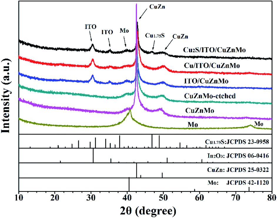 | ||
| Fig. 2 XRD patterns of prepared multilayer Mo, CuZnMo, CuZnMo-etched, ITO/CuZnMo, Cu/ITO/CuZnMo and Cu2S/ITO/CuZnMo films. | ||
The large specific surface area in the multilayer CEs is designed to arise from the porous structures of the etched alloy layer. The evolution of the morphology and thickness of the films at different stages, magnetron sputtering, etching, and in situ sulfidation, was investigated and is shown in Fig. 3. The CuZnMo alloy layer and the Mo-based film have uniform thickness and a smooth interface, and the upper and lower layers have good adhesion (Fig. 3a and f), which is favourable for maintaining the overall composition and morphologies in the subsequent etching process. After the CuZnMo film was etched with hydrochloric acid, a flat porous CuZnMo conductive film was obtained with a large pore size and an average thickness of about 1.2 μm (Fig. 3b and g). Benefitting from the high electrical conductivity and corrosion resistance of the sputtered ITO layer, ITO/CuZnMo structured film could be used as a protective film (Fig. 3c and h). ITO grows along the direction of the hole and acts as a protective layer in three-dimensional directions. After 20 min of magnetron sputtering deposition, a Cu film composed of Cu nanoparticles was formed on the ITO/CuZnMo film. The Cu nanoparticles were not only distributed uniformly, but were also attached closely to the ITO/CuZnMo film, forming a Cu/ITO/CuZnMo multilayer film (Fig. 3d and i). The subsequent polysulfide treatment resulted in the transformation of compact Cu film into a porous Cu2S film with a thickness of 480 nm, and produced a Cu2S/ITO/CuZnMo multilayer film, as shown in Fig. 3e and j. Transformed Cu2S displayed a uniformly distributed porous nanosheet shape, providing a larger specific surface area for the electrolyte and providing high catalytic activity to the CE.45 It is worth noting that the adhesion between Cu2S and the substrate is affected by the flatness of the ITO/CuZnMo substrate. The rougher the substrate is, the greater the adhesion will be. There are several reports about Cu2S-based CEs that were prepared by using FTO/ITO glass as the substrate.32,43,45,46,50 The utilization of FTO/ITO glass as substrates for CE in QDSCs facilitates the whole process and reduces the cost for commercial accessibility. However, adhesion forces between Cu2S and the FTO/ITO glass substrate were simultaneously lowered to some extent because of their flatness. In the present work, a porous ITO/CuZnMo film substrate is designed to promote the adhesion of the following Cu2S film and the resistance of the CE to electrolyte corrosion.
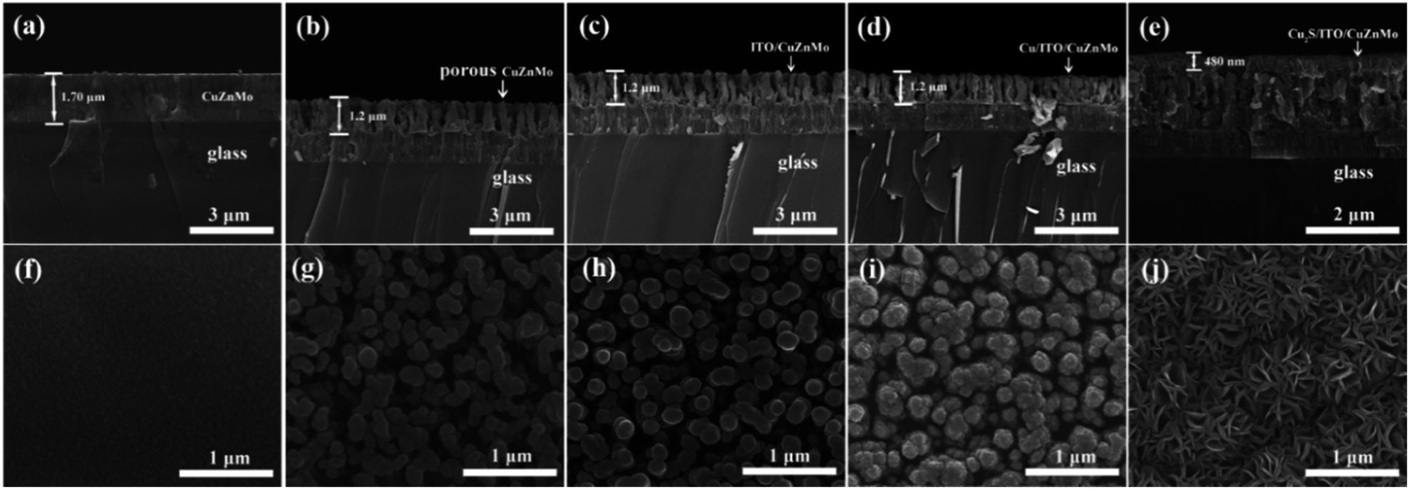 | ||
| Fig. 3 SEM micrographs of surface and cross-section of (a and f) CuZnMo conductive film, (b and g) porous CuZnMo conductive film, (c and h) porous ITO/CuZnMo film, (d and i) Cu/ITO/CuZnMo film, (e and j) Cu2S/ITO/CuZnMo film. | ||
The roles of conduction and resistance of CEs to electrolyte corrosion can be enhanced, depending on the sputtered ITO layer in multilayer CEs. To improve the corrosion resistance of the final multilayer Cu2S/ITO/CuZnMo functionalized film CEs to polysulfide electrode solution, heat treatment to sputtered ITO/glass films was performed prior to Cu deposition by magnetron sputtering. The average thickness of the film is approximately 200 nm when the ITO deposition time is 30 min, as shown in Fig. S1.† It is found that the ITO film has good adhesion to glass, and large particles are distributed upon the ITO film, which grows mainly in columns and has small bulges at the top. Fig. S2† shows the XRD patterns of the obtained ITO/glass films after annealing at different temperatures under an atmosphere of pure nitrogen. The diffraction peaks of the ITO/glass film prepared at room temperature are weak. By comparison, sharper diffraction peaks of (211), (222), (400), (440), and (622) planes are present for the annealed ITO/glass films, confirming a cubic phase after annealing at a temperature higher than 300 °C. When magnetron sputtering on a glass substrate is performed at room temperature, the lower mobility of the deposited atoms causes the deposited particles to grow mainly as island shapes, and the probability of formation of an impurity phase increases, resulting in structural defects and non-stoichiometric ingredients of ITO/glass films. The high-temperature annealing process facilitates the rearrangement of oxide atoms of nonstoichiometric components, such as In2O3−x and SnO2−x. An obvious increase in the intensities of the diffraction peaks can be observed with higher annealing temperatures, implying the ITO films are formed with higher crystallinity.
In order to further investigate the effect of annealing temperature on ITO/glass films, the surface morphology of the film was characterized by AFM. AFM 3D diagrams of the ITO/glass films annealed under nitrogen atmosphere are shown in Fig. 4. As annealing temperature increases, the surface of ITO/glass films becomes more compact with less roughness and the size of grains is increased, indicating that heat treatment under a higher temperature is beneficial to the regrowth of the grains and improves the compactness of the films. In order to demonstrate that the high-temperature annealed ITO/glass film has better electrical properties, resistance analysis of the ITO/glass films annealed at different temperatures was carried out using a four-probe method. The experimental results are shown in Fig. S3.† It is found that the annealing temperature has an obvious influence on the resistance of ITO/glass films. Originally, oxygen vacancies exist in ITO films due to the different deposition rates between cation and anion during the process of ITO sputtering. Simultaneously, some absorbed oxygen atoms escape from the surface of the ITO film, when the oxygen is insulated during the annealing process at high temperature. The original and escaped oxygen vacancies can serve as two weakly bound electrons for the donor by itself, making the defect semiconducting and increasing carrier concentrations. Finally, the atoms are rearranged to form polycrystalline films and lowering the resistivity of the ITO films. The sheet resistance of the deposited ITO/glass films falls from about 700 to 10 Ω sq−1, when the annealing temperature increases from room temperature to 500 °C under a nitrogen atmosphere. Accordingly, the resistivities of the films fall from 1.06 × 10⁻² Ω cm to 2.28 × 10⁻⁴ Ω cm. We also conducted the annealing of ITO/glass film at as high a temperature as 600 °C, and found that the final sheet resistance value is about 40 Ω sq−1. However, the higher temperature caused the cracking of CuZnMo films.
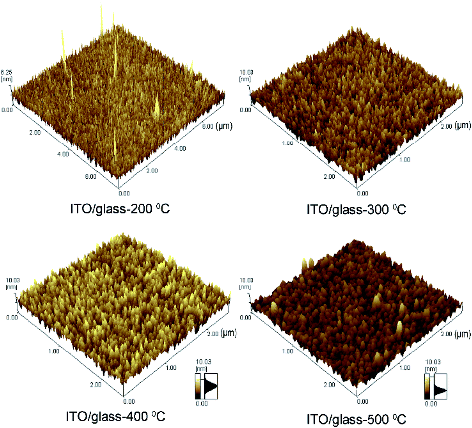 | ||
| Fig. 4 AFM 3D images of ITO/glass films annealed under a pure nitrogen atmosphere at different temperatures. | ||
To demonstrate the electrocatalytic activity and corrosion resistance of the multilayer Cu2S/ITO(T)/CuZnMo functionalized film CEs, the photovoltaic performance of CuInS2 QDSCs based on the CEs was investigated. The J–V curves of the CuInS2 QDSCs under the illumination of an AM 1.5G solar simulator with an intensity of 100 mW cm−2 (1 full sun) are shown in Fig. 5a, and the extracted photovoltaic parameters are summarized in Table 1. It should be noted that the photovoltaic performance measurements were conducted on at least five cells. Swapping of a brass-based CE for the multilayer Cu2S/ITO/CuZnMo CE reduces the PCE of the QDSCs, if the corresponding ITO protective layers are annealed below 300 °C. When the annealing temperature of the ITO protective layers increases to 400/500 °C, the QDSCs based on the multilayer Cu2S/ITO/CuZnMo film CEs exhibit a better photovoltaic performance with a higher Jsc, Voc, FF and PCE than those of QDSCs based on brass-based CEs, partially because of their improved electrical properties and conductivities of the CEs. A PCE of 4.40% with Jsc of 16.81 ± 0.04 mA cm−2, Voc of 535.4 ± 0.9 mV and FF of 48.84 ± 0.04% is achieved for QDSCs based on a multilayer Cu2S/ITO(500 °C)/CuZnMo film CE. The PCE of the QDSCs increases by 13.6% compared with that of a multilayer Cu2S/ITO(200 °C)/CuZnMo film CE. As the annealing temperature of the ITO protective layer increases, the CE films exhibit a more crystalline structure. Both the resistivity of the ITO films and the sheet resistance of the CEs decrease, resulting in enhanced conductivity of the CEs. This probably leads to a better FF and PCE of the corresponding QDSCs. When the annealing temperature of the ITO protective layer is higher than 500 °C, the ITO films begin to crack; hence the sheet resistivity of the CEs increases, which is consistent with a previous report.51
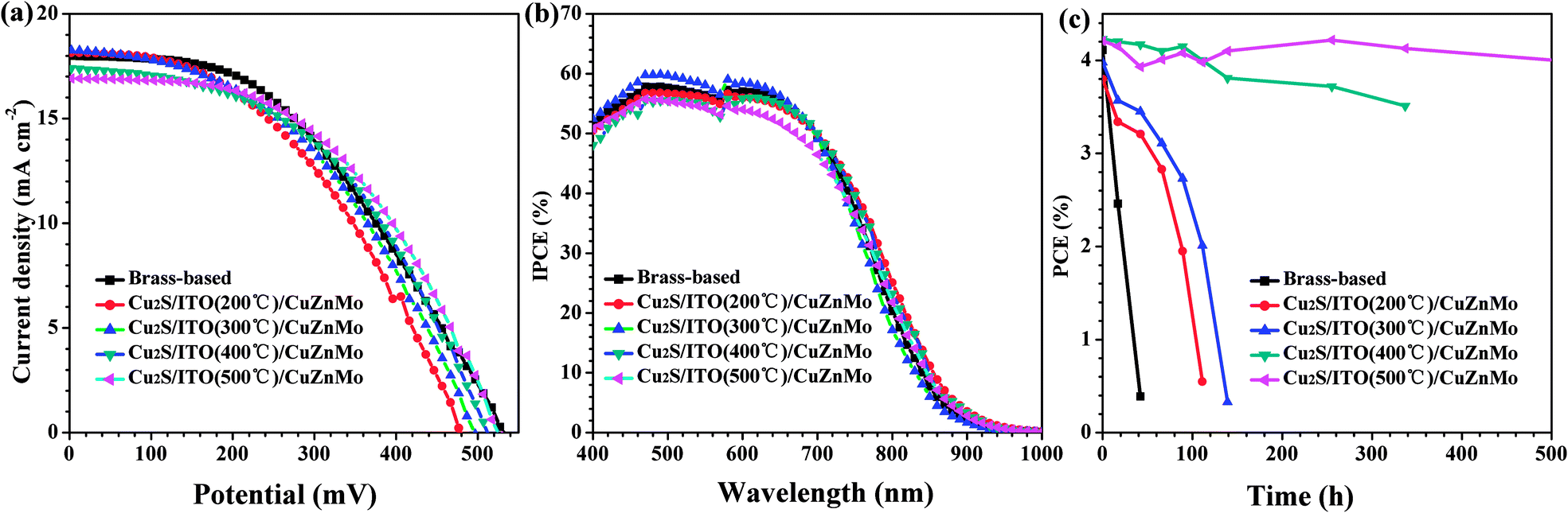 | ||
| Fig. 5 (a) J–V curves and (b) IPCE spectra of QDSCs using different multilayer Cu2S/ITO(T)/CuZnMo functional films and brass-based CEs, and (c) PCE stability of QDSCs assembled with different CEs. | ||
| CEs | J sc (mA cm−2) | V oc (mV) | FF (%) | PCE (%) |
|---|---|---|---|---|
| a Average values of at least five different cells. | ||||
| Brass-based | 17.89 ± 0.22 | 534.9 ± 4.1 | 43.62 ± 0.8 | 4.17 ± 0.01 |
| Cu2S/ITO(200 °C)/CuZnMo | 17.91 ± 0.45 | 486.1 ± 2.3 | 44.59 ± 1.75 | 3.87 ± 0.22 |
| Cu2S/ITO(300 °C)/CuZnMo | 17.44 ± 0.98 | 486.9 ± 2.9 | 44.45 ± 0.11 | 3.86 ± 0.23 |
| Cu2S/ITO(400 °C)/CuZnMo | 17.26 ± 0.10 | 515.3 ± 3.5 | 47.85 ± 0.46 | 4.24 ± 0.03 |
| Cu2S/ITO(500 °C)/CuZnMo | 16.81 ± 0.04 | 535.4 ± 0.9 | 48.84 ± 0.04 | 4.40 ± 0.01 |
The IPCE represents the number of photo-generated charge carriers that contribute to the current of each incident photon. The IPCE curves of the QDSCs fabricated with different CEs shown in Fig. 5b are basically similar. QDSCs based on multilayer Cu2S/ITO(300 °C)/CuZnMo functionalized film CE show the maximum IPCE of about 60% in the range from 460 nm to 650 nm, which is higher than the value for the QDSCs based on a brass-based CE. The difference between current densities measured from the J–V curves tested under AM 1.5G illumination and calculated by integrating IPCE spectra is thought to be caused by the low efficiencies of charge separation and collection under limited light intensity from the monochromator in the IPCE.
To characterize the stability of the assembled QDSCs using the multilayer Cu2S/ITO(T)/CuZnMo functionalized film CEs, QDSCs were sealed and tested under successive irradiation via an AM 1.5G solar simulator with an intensity of 100 mW cm−2 at room temperature. As shown in Fig. 5c, the annealing temperature of the ITO protective film is positively related to the stability of the corresponding QDSCs. And the high annealing temperature is beneficial for improving the stability of the QDSCs. The PCE of QDSCs assembled with a multilayer Cu2S/ITO(500 °C)/CuZnMo functionalized film CE degrades from an initial 4.21% to a final 4.00% with a negligible drop of 5% after 500 h of irradiation. In comparison, the PCE of QDSCs assembled with a brass-based CE had dropped 40% after only 17 h, and the QDSCs basically failed after 24 h. In fact, the QDSCs assembled with brass-based CEs are hard to seal because of the porous surface of Cu2S CEs after sulfidation from etched brass. It is clear that the multilayer Cu2S/ITO(400/500 °C)/CuZnMo functionalized film CEs demonstrate improved stability compared to brass-based CEs, indicating that the multilayer Cu2S/ITO(500 °C)/CuZnMo functionalized film CE has enhanced resistance to electrolyte corrosion and good stability. The improved stability of the corresponding QDSCs was firstly attributed to the flatter surface of CEs than brass-based CEs, and also derived from enhanced adhesion strength between 400/500 °C annealed ITO film and porous alloy structures after HCl etching.
The catalytic activity derived from Cu2S is enabled by Cu sputtering and following sulfidation. In this work, the influence of Cu2S film thickness after in situ sulfidation was further investigated. Surface and cross-section micrographs of Cu2S(t) film on the porous ITO/CuZnMo structured films were characterized and are shown in Fig. 6. The Cu film is sulfated along the pores to obtain following Cu2S nanosheets. With the increase in Cu sputtering time, the stacking of Cu2S nanosheets greatly improves the thickness of the films. When the sputtering time is less than 20 min, there are only the spherical nanosheets after sulfidation, due to the sputtering time of Cu film being too short to maintain the porous structure. The thickness of the obtained Cu2S layer is about 480 nm at a deposition time of 20 min. The thickness of the Cu2S layer increases from about 746 nm to 1.95 μm, with the time of Cu deposition increasing from 30 to 60 min. When the sputtering time is 40 min, as shown in Fig. 6d and i, Cu2S nanosheet layers with thickness of about 1.2 μm are obtained after sulfidation, which still have good adhesion with the porous ITO/CuZnMo structured film. The adhesion of catalytic materials with the resulting conductive substrate determines the performance of QDSCs.52 The catalytic materials in the CE might fall from the substrate without enough adhesion, which will thereby weaken the long-term photovoltaic performance of the QDSCs. In addition, the thickness of the catalytic materials also determines the catalytic activity of the electrode. A thin Cu2S layer cannot provide sufficient active sites for the redox couple of the polysulfide electrolyte, while too thick a Cu2S layer can reduce the adhesion strength that may cause small amounts of Cu2S nanosheets to fall from the porous ITO/CuZnMo structured films.
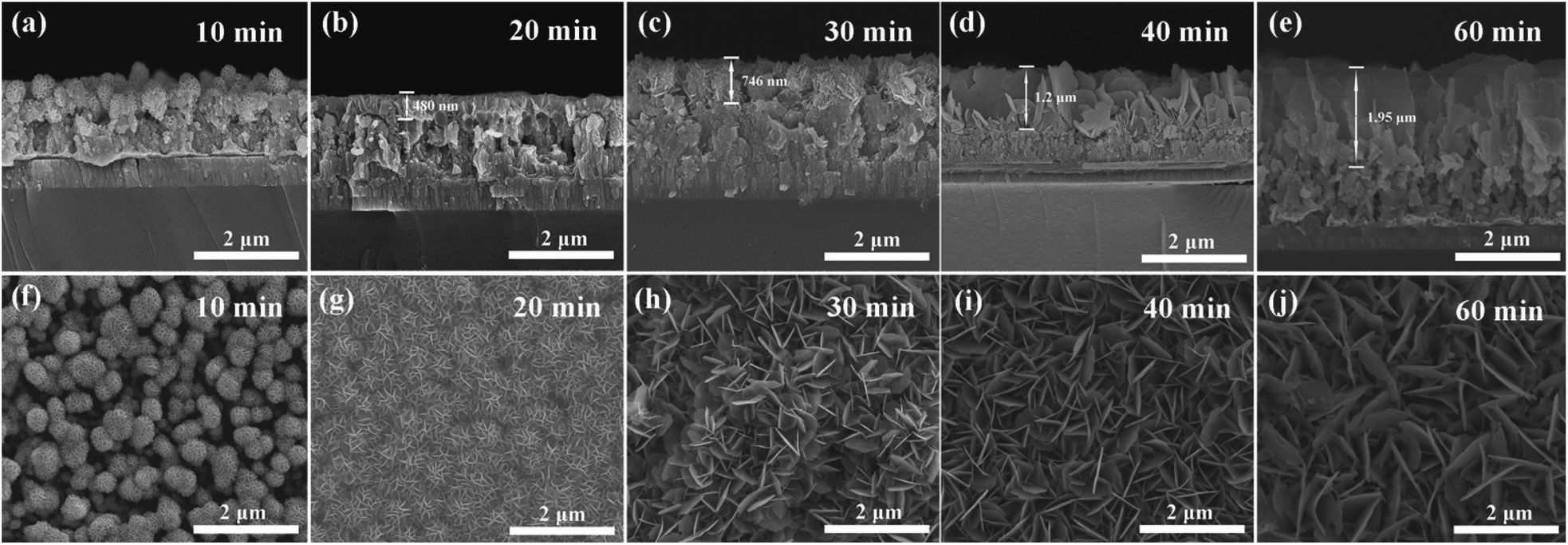 | ||
| Fig. 6 SEM micrographs of surface and cross-section of multilayer Cu2S(t)/ITO/CuZnMo functional film prepared at different Cu sputtering times: (a and f) 10 min, (b and g) 20 min, (c and h) 30 min, (d and i) 40 min, (e and j) 60 min. | ||
To demonstrate the electrocatalytic activity of the multilayer Cu2S(t)/ITO/CuZnMo functionalized film CEs for the polysulfide electrolyte, the photovoltaic performance of the QDSCs fabricated with the multilayer Cu2S(t)/ITO/CuZnMo functionalized film CEs at different deposition times were investigated. The J–V curves of the solar cells under the illumination of an AM 1.5G solar simulator with an intensity of 100 mW cm−2 (1 full sun) are shown in Fig. 7a, and the extracted photovoltaic parameters are summarized in Table 2. The QDSCs based on multilayer Cu2S(t)/ITO/CuZnMo functionalized film CEs exhibit better photovoltaic performance than those based on brass-based CEs, which suffer from continuous corrosion of the brass alloy by the electrolyte. A PCE of 5.21%, with Jsc of 18.50 mA cm−2, Voc of 533.1 mV and FF of 52.84% is achieved for QDSCs based on the multilayer Cu2S(40 min)/ITO/CuZnMo functionalized film CE. As the Cu2S film in the CE becomes thicker, the total amount of the Cu2S nanosheets increases and the electrode presents more catalytic sites, probably providing more active sites for polysulfide electrolytes and thus enhancing the performance of the QDSCs. In contrast, a thinner Cu2S film in a CE cannot provide sufficient active sites for the redox couple of the polysulfide electrolyte, resulting in a PCE of 4.17% for QDSCs based on the multilayer Cu2S(10 min)/ITO/CuZnMo functionalized film CE. It is also found that too thick a Cu2S layer has worse adhesion with the porous ITO/CuZnMo structured film and can easily fall off, which may result in a deterioration of the photovoltaic performance of the QDSCs.
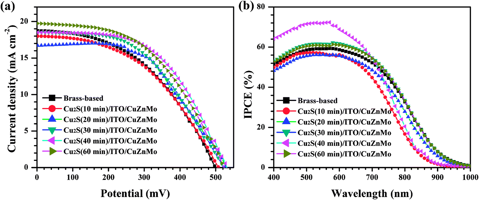 | ||
| Fig. 7 (a) J–V curves and (b) IPCE spectra of QDSCs using different multilayer Cu2S(t)/ITO/ZnMo functional films and brass-based CEs. | ||
| CEs | J sc (mA cm−2) | V oc (mV) | FF (%) | PCE (%) |
|---|---|---|---|---|
| a Average values of at least five different cells. b Best performance of QDSCs based on Cu2S(40 min)/ITO/CuZnMo CE. | ||||
| Brass-based | 18.78 ± 0.47 | 494.8 ± 3.1 | 45.92 ± 0.26 | 4.22 ± 0.01 |
| Cu2S(10 min)/ITO/CuZnMo | 17.88 ± 0.05 | 508.8 ± 4.7 | 45.92 ± 0.16 | 4.17 ± 0.02 |
| Cu2S(20 min)/ITO/CuZnMo | 17.07 ± 0.22 | 535.8 ± 3.0 | 48.26 ± 1.67 | 4.41 ± 0.14 |
| Cu2S(30 min)/ITO/CuZnMo | 18.72 ± 0.12 | 526.6 ± 6.8 | 47.50 ± 0.56 | 4.64 ± 0.06 |
| Cu2S(40 min)/ITO/CuZnMo | 18.63 ± 0.09 | 532.6 ± 0.2 | 52.16 ± 0.42 | 5.18 ± 0.02 |
| Cu2S(60 min)/ITO/CuZnMo | 19.68 ± 0.04 | 532.8 ± 4.5 | 47.69 ± 0.33 | 5.00 ± 0.09 |
| Cu2S(40 min)/ITO/CuZnMo | 18.50 | 533.1 | 52.84 | 5.21 |
Fig. 7b shows the IPCE spectra of QDSCs based on different CEs. The QDSCs based on the nanosheet Cu2S layer display almost the same spectral response ranges from 400 nm to 1000 nm and close IPCE values, since they have the same photoanode and electrolyte. The IPCE curve of QDSCs based on a multilayer Cu2S(40 min)/ITO/CuZnMo functionalized film CE exhibits a strong photoresponse (maximum 72%) over the window below 600 nm, higher than those of the other QDSCs based on Cu2S/ITO/CuZnMo functionalized CEs or brass-based CE (58%), indicating the better electrocatalytic activity of the multilayer Cu2S(40 min)/ITO/CuZnMo functionalized film CE, which is consistent with the J–V curves.
In order to reveal the nature of the better electrochemical characteristics of the multilayer Cu2S(t)/ITO/CuZnMo functionalized film CEs compared to brass-based CEs, EIS was performed to analyse charge transfer resistance (Rct) in the interface of the CEs and the electrolyte.53–55Fig. 8a shows the Nyquist plots of symmetrical thin-layer cells based on different CEs measured at zero bias potential over the frequency range of 0.1 Hz to 100 kHz under dark conditions. The illustration shows the EIS Nyquist enlarged view and equivalent circuit diagram, and the fitting results are listed in Table 3. Rs is the series resistance of symmetrical thin-layer cells, and Rct is the charge transfer resistance and CPE in the equivalent circuit represents the corresponding constant phase angle at the CE/electrolyte interface and the photoanode/electrolyte interface. It is found that the multilayer Cu2S(t)/ITO/CuZnMo functionalized film CEs have small Rs values (less than 4 Ω) comparable with brass-based CEs, suggesting good conductivity and close contact between Cu2S and the porous ITO/CuZnMo structured film. The Rct values of all the multilayer Cu2S(t)/ITO/CuZnMo functionalized film CEs are far lower than those of brass-based CEs. In particular, the multilayer Cu2S(40 min)/ITO/CuZnMo functionalized film CE has an Rct as low as 0.57 Ω. A reduced Rct would lead to a higher FF, and thereby an enhanced PCE, which are consistent with the difference in the photovoltaic performance of QDSCs.
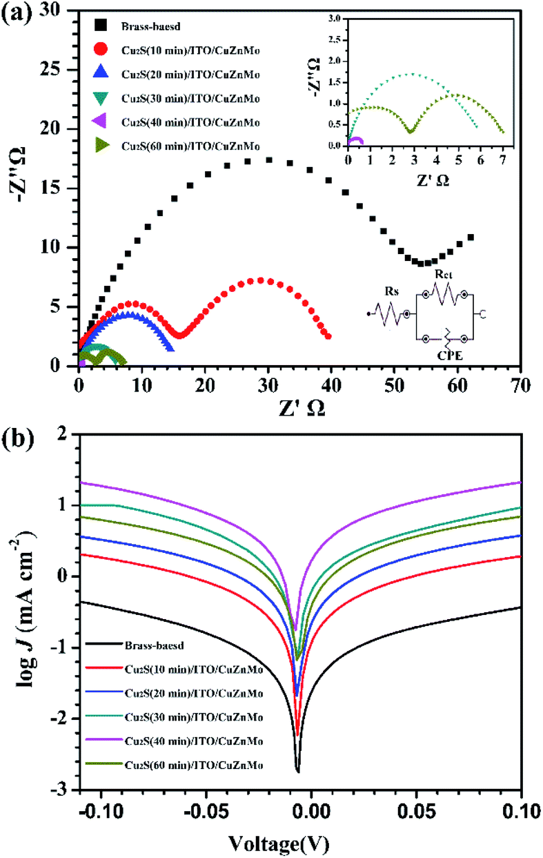 | ||
| Fig. 8 (a) EIS Nyquist diagram; (b) Tafel polarization curves of symmetric cells based on multilayer Cu2S(t)/ITO/CuZnMo functional films and brass-based CEs. | ||
| CEs | R s (Ω) | R ct (Ω) | CPE |
|---|---|---|---|
| Brass-based | 7.36 | 58.5 | 3.7 × 10⁻⁵ |
| Cu2S(10 min)/ITO/CuZnMo | 16.1 | 17.3 | 8.6 × 10⁻⁵ |
| Cu2S(20 min)/ITO/CuZnMo | 1.03 | 15.1 | 1.1 × 10⁻⁵ |
| Cu2S(30 min)/ITO/CuZnMo | 0.79 | 5.81 | 1.6 × 10⁻² |
| Cu2S(40 min)/ITO/CuZnMo | 3.36 | 0.57 | 5.9 × 10⁻³ |
| Cu2S(60 min)/ITO/CuZnMo | 1.53 | 5.95 | 1.8 × 10⁻² |
To further verify the electrochemical performance of the multilayer Cu2S(t)/ITO/CuZnMo functionalized film CEs, Tafel polarization curves were also measured and are shown in Fig. 8b. Here Cu2S(t)/ITO/CuZnMo in the figure is replaced by the abbreviation Cu2S(t)-CE for the convenience of drawing. The catalytic activity of the CE can be seen from the current density at equilibrium J0. It is inversely proportional to Rct in EIS and is calculated from equation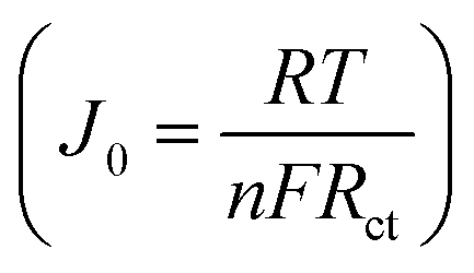 (where n represents the number of electrons involved in the polysulfide reduction, F is the Faraday constant, and R is the gas constant, and J0 is related to the steep gradient of the cathode and anode branches). The steep slope indicates that the J0 value is large, and the electrode has a better catalytic performance. The multilayer Cu2S(40 min)/ITO/CuZnMo functionalized film has the largest J0 value, implying the best catalytic activity, which is consistent with the J–V measurements above, and the regularity is consistent with the EIS test results.
4 Conclusions
Multilayer Cu2S/ITO/CuZnMo functional film CEs were prepared by magnetron sputtering, etching, and in situ sulfidation. These CEs achieved a large specific surface area arising from the porous structures of the etched alloy layer, good conductivity and resistance to electrolyte corrosion originating from the annealed ITO layer, and high catalytic activity provided by the Cu2S layer. The annealing of the ITO/glass film at 500 °C reduced the electrical resistivity from 1.06 × 10⁻² Ω cm to 2.28 × 10⁻⁴ Ω cm. The QDSCs based on multilayer Cu2S/ITO(500 °C)/CuZnMo functionalized films exhibit enhanced resistance to electrolyte corrosion, high catalytic activity and good stability with the PCE maintained at 4.00% after 500 h of irradiation. The multilayer Cu2S(40 min)/ITO/CuZnMo functionalized films possess the best performance of Cu2S with a thickness of 1.2 μm and an Rct of 0.57 Ω. The best photovoltaic performance of QDSCs based on multilayer Cu2S/ITO/CuZnMo functionalized films is achieved with a PCE of 5.21% (Voc = 533.1 mV, Jsc = 18.80 mA cm−2, FF = 52.84%) under AM 1.5 radiation (1 full sun) illumination with an incident power of 100 mW cm−2. The design strategy on multilayer films could be adapted to other efficient CEs beyond QDSCs.Conflicts of interest
There are no conflicts to declare.Acknowledgements
This work was financially supported by the funds from the National Natural Science Foundation of China (51572199, 51772218, 61471270) and the Key Lab of Novel Thin Film Solar Cells, Chinese Academy of Sciences (KF201603).References
- A. Zaban, O. I. Mićić, B. A. Gregg and A. J. Nozik, Langmuir, 1998, 14, 3153–3156 CrossRef CAS.
- R. Vogel, K. Pohl and H. Weller, Chem. Phys. Lett., 1990, 174, 241–246 CrossRef CAS.
- Z. Pan, H. Rao, I. Mora-Seró, J. Bisquert and X. Zhong, Chem. Soc. Rev., 2018, 47, 7659–7702 RSC.
- Z. Pan, K. Zhao, J. Wang, H. Zhang, Y. Feng and X. Zhong, ACS Nano, 2013, 7, 5215–5222 CrossRef CAS PubMed.
- M. Booth, A. P. Brown, S. D. Evans and K. Critchley, Chem. Mater., 2012, 24, 2064–2070 CrossRef CAS.
- A. D. Leach and J. E. Macdonald, J. Phys. Chem. Lett., 2016, 7, 572 CrossRef CAS.
- Z. Pan, L. Yue, H. Rao, J. Zhang, X. Zhong, Z. Zhu and A. K.-Y. Jen, Adv. Mater., 2019, 31, 1903696 CrossRef CAS.
- W. Shockley and H. J. Queisser, J. Appl. Phys., 1961, 32, 510–519 CrossRef CAS.
- R. D. Schaller, V. M. Agranovich and V. I. Klimov, Nat. Phys., 2015, 1, 189–194 Search PubMed.
- S. Gorer and G. Hodes, J. Phys. Chem., 1994, 98, 5338–5346 CrossRef CAS.
- G. S. Selopal, H. Zhao, G. Liu, H. Zhang, X. Tong, K. Wang, J. Tang, X. Sun, S. Sun, F. Vidal, Y. Wang, Z. M. Wang and F. Rosei, Nano Energy, 2019, 55, 377–388 CrossRef CAS.
- L. Zhang, H. Rao, Z. Pan and X. Zhong, ACS Appl. Mater. Interfaces, 2019, 11, 41415–41423 CrossRef CAS PubMed.
- R. S. Dibbell and D. F. Watson, J. Phys. Chem. C, 2009, 113, 3139–3149 CrossRef CAS.
- A. Tubtimtae and M. W. Lee, Thin Solid Films, 2012, 526, 225–230 CrossRef CAS.
- J. H. Bang and P. V. Kamat, Adv. Funct. Mater., 2010, 20, 1970–1976 CrossRef CAS.
- S. S. Mali, S. K. Desai, S. S. Kalagi, C. A. Betty, P. N. Bhosale, R. S. Devan, Y. R. Ma and P. S. Patil, Dalton Trans., 2012, 41, 6130–6136 RSC.
- J. Jiao, Z. Zhou, W. Zhou and S. Wu, Mater. Sci. Semicond. Process., 2013, 16, 435–440 CrossRef CAS.
- A. Tubtimtae, M. W. Lee and G. J. Wang, J. Power Sources, 2011, 196, 6603–6608 CrossRef CAS.
- N. Balis, V. Dracopoulos, K. Bourikas and P. Lianos, Electrochim. Acta, 2013, 91, 246–252 CrossRef CAS.
- L. C. Chen, Y. C. Ho, R. Y. Yang, J. H. Chen and C. M. Huang, Appl. Surf. Sci., 2012, 258, 6558–6563 CrossRef CAS.
- H. Mcdaniel, N. Fuke, J. M. Pietryga and V. I. Klimov, J. Phys. Chem. Lett., 2013, 4, 1059 CrossRef CAS PubMed.
- C. Steinhagen, M. G. Panthani, V. Akhavan, B. Goodfellow, B. Koo and B. A. Korgel, J. Am. Chem. Soc., 2009, 131, 12554–12555 CrossRef CAS PubMed.
- H. Song, H. Rao and X. Zhong, J. Mater. Chem. A, 2018, 6, 4895–4911 RSC.
- G. Hodes, J. Phys. Chem. C, 2008, 112, 17778–17787 CrossRef CAS.
- V. Jovanovski, V. González-Pedro, S. Giménez, E. Azaceta, G. Cabañero, H. Grande, R. Tena-Zaera, I. Mora-Seró and J. Bisquert, J. Am. Chem. Soc., 2011, 133, 20156–20159 CrossRef CAS PubMed.
- V. Chakrapani, D. Baker and P. V. Kamat, J. Am. Chem. Soc., 2011, 133, 9607–9615 CrossRef CAS PubMed.
- A. Hauch and A. Georg, Electrochim. Acta, 2002, 46, 3457–3466 CrossRef.
- G. Hodes, J. Manassen and D. Cahen, J. Appl. Electrochem., 1977, 7, 181–182 CrossRef CAS.
- L. Quan, W. Li, L. Zhu, H. Geng, X. Chang and H. Liu, J. Power Sources, 2014, 272, 546–553 CrossRef CAS.
- J. Wang, I. Mora-Seró, Z. Pan, K. Zhao, H. Zhang, Y. Feng, G. Yang, X. Zhong and J. Bisquert, J. Am. Chem. Soc., 2013, 135, 15913–15922 CrossRef CAS PubMed.
- P. K. Santra and P. V. Kamat, J. Am. Chem. Soc., 2012, 134, 2508–2511 CrossRef CAS PubMed.
- A. D. Savariraj, K. K. Viswanathan and K. Prabakar, ACS Appl. Mater. Interfaces, 2014, 6, 19702–19709 CrossRef CAS PubMed.
- C. Y. Lin, C. Y. Teng, T. L. Li, Y. L. Lee and H. Teng, J. Mater. Chem. A, 2013, 1, 1155–1162 RSC.
- Y. Lin, H. Song, H. Rao, Z. Du, Z. Pan and X. Zhong, J. Phys. Chem. Lett., 2019, 10, 4974–4979 CrossRef CAS PubMed.
- S. Thomas, T. G. Deepak, G. S. Anjusree, T. A. Arun, S. V. Nair and A. S. Nair, J. Mater. Chem. A, 2014, 2, 4474–4490 RSC.
- Y. Jiang, X. Zhang, Q. Q. Ge, B. B. Yu, Y. G. Zou, W. J. Jiang, W. G. Song, L. J. Wan and J. S. Hu, Nano Lett., 2014, 14, 365 CrossRef CAS PubMed.
- M. H. Yeh, C. P. Lee, C. Y. Chou, L. Y. Lin, H. Y. Wei, C. W. Chu, R. Vittal and K. C. Ho, Electrochim. Acta, 2011, 57, 277–284 CrossRef CAS.
- T. Shu and Z. L. Ku, J. Alloys Compd., 2014, 586, 257–260 CrossRef CAS.
- G. Hodes, J. Manassen and D. Cahen, J. Electrochem. Soc., 1980, 127, 544–549 CrossRef CAS.
- S. Giménez, I. Mora-Seró, L. Macor, N. Guijarro, T. Lana-Villarreal, R. Gómez, L. J. Diguna, Q. Shen, T. Toyoda and J. Bisquert, Nanotechnology, 2009, 20, 295204 CrossRef PubMed.
- K. Zhao, H. Yu, H. Zhang and X. Zhong, J. Phys. Chem. C, 2014, 118, 5683–5690 CrossRef CAS.
- X. Q. Chen, Z. Li, Y. Bai, Q. Sun, L. Z. Wang and S. X. Dou, Chem.–Eur. J., 2015, 21, 1055–1063 CrossRef CAS PubMed.
- F. Wang, D. Hui, J. Pan, J. Li, L. Qi and D. Xu, J. Phys. Chem. C, 2014, 118, 19589–19598 CrossRef CAS.
- Z. Du, Z. Pan, F. Fabregatsantiago, Z. Ke, D. Long, Z. Hua, Y. Zhao, X. Zhong, J. S. Yu and J. Bisquert, J. Phys. Chem. Lett., 2016, 7, 3103–3111 CrossRef CAS.
- M. Ke, P. K. Surolia, O. Byrne and K. R. Thampi, J. Power Sources, 2014, 248, 218–223 CrossRef.
- Y. Wang, Q. Zhang, Y. Li and H. Wang, J. Power Sources, 2016, 318, 128–135 CrossRef CAS.
- J. Du, Z. Du, J. S. Hu, Z. Pan, Q. Shen, J. Sun, D. Long, H. Dong, L. Sun and X. Zhong, J. Am. Chem. Soc., 2016, 138, 4201–4209 CrossRef CAS PubMed.
- C. Cai, L. Zhai, Q. Wu, Y. Ma, L. Zhang, Y. Yang, C. Zou and S. Huang, J. Alloys Compd., 2017, 719, 227–235 CrossRef CAS.
- C. Cai, L. Zhai, Y. Ma, C. Zou, L. Zhang, Y. Yang and S. Huang, J. Power Sources, 2017, 341, 11–18 CrossRef CAS.
- S. Wang and J. Tian, RSC Adv., 2016, 6, 90082–90099 RSC.
- L. J. Meng and M. P. D. Santos, Thin Solid Films, 1996, 426, 65–69 CrossRef.
- J. G. Radich, R. Dwyer and P. V. Kamat, J. Phys. Chem. Lett., 2015, 2, 2453–2460 CrossRef.
- W. Qing, I. Seigo, G. T. Michael, F. S. Francisco, M. S. Iván, B. Juan, B. Takeru and I. Hachiro, J. Phys. Chem. B, 2006, 110, 25210–25221 CrossRef PubMed.
- E. M. Barea, S. Menny, G. Sixto, H. Idan, M. S. Iván, Z. Arie and B. Juan, J. Am. Chem. Soc., 2010, 132, 6834–6839 CrossRef CAS PubMed.
- G. P. Victoria, X. Xueqing, M. S. Iván and B. Juan, ACS Nano, 2010, 4, 5783–5790 CrossRef PubMed.
Footnote |
| † Electronic supplementary information (ESI) available: SEM images of surface and cross-section of ITO/glass, resistance and resistivity analysis of ITO/glass film after annealing. See DOI: 10.1039/c9na00654k |
| This journal is © The Royal Society of Chemistry 2020 |