
 Open Access Article
 This Open Access Article is licensed under a
 Creative Commons Attribution 3.0 Unported Licence
In-plane anisotropic electronics based on low-symmetry 2D materials: progress and prospects
Siwen
Zhao
 a,
Baojuan
Dong
bc,
Huide
Wang
a,
Hanwen
Wang
bc,
Yupeng
Zhang
a,
Zheng Vitto
Han
*bc and
Han
Zhang
*a
a,
Baojuan
Dong
bc,
Huide
Wang
a,
Hanwen
Wang
bc,
Yupeng
Zhang
a,
Zheng Vitto
Han
*bc and
Han
Zhang
*a
aInternational Collaborative Laboratory of 2D Materials for Optoelectronics Science Technology of Ministry of Education, Key Laboratory of Optoelectronic Devices and Systems of Ministry of Education and Guangdong Province, Shenzhen University, Shenzhen 518060, China. E-mail: hzhang@szu.edu.cn
bShenyang National Laboratory for Materials Science, Institute of Metal Research, Chinese Academy of Sciences, Shenyang 110000, China. E-mail: vitto.han@gmail.com
cSchool of Material Science and Engineering, University of Science and Technology of China, Anhui 230026, China
First published on 6th December 2019
Abstract
Low-symmetry layered materials such as black phosphorus (BP) have been revived recently due to their high intrinsic mobility and in-plane anisotropic properties, which can be used in anisotropic electronic and optoelectronic devices. Since the anisotropic properties have a close relationship with their anisotropic structural characters, especially for materials with low-symmetry, exploring new low-symmetry layered materials and investigating their anisotropic properties have inspired numerous research efforts. In this paper, we review the recent experimental progresses on low-symmetry layered materials and their corresponding anisotropic electrical transport, magneto-transport, optoelectronic, thermoelectric, ferroelectric, and piezoelectric properties. The boom of new low-symmetry layered materials with high anisotropy could open up considerable possibilities for next-generation anisotropic multifunctional electronic devices.
1. Introduction
Two dimensional (2D) layered materials with strong in-plane covalent bonds and weak out-of-plane van der Waals interactions span a very broad range of solids and exhibit extraordinary and unique layer-dependent physical properties after the discovery of graphene.1–6 Even though graphene has extremely large mobility and outstanding electron-transport properties, the absence of a band gap restricts its applications in (opto)electronic devices. Beyond graphene, 2D layered materials have become more and more popular among researchers due to their unique structural,7,8 mechanical,9 electrical,10,11 thermoelectric,12–15 optical,16–22 catalytic,23,24 and sensing properties,.25–30 Transition metal dichalcogenides (TMDCs) with tunable band gap fully exert the advantages in low-cost, flexible, and high-performance logic and optoelectronic devices, such as field-effect transistors (FETs), photodetectors, photonic devices and solar cells. However, people mainly focus on the in-plane isotropic behaviors in graphene and TMDCs because of their symmetric crystal structures until the rediscovery of low-symmetry black phosphorus (BP).It is known that reducing the symmetry of materials is generally associated with exceptional anisotropy in electronic energy band structure and can be regarded as a process of lowering the dimensionality of the carrier transport. Therefore, the electrical, optical, thermal, and phonon properties of these anisotropic materials are diverse along the different in-plane crystal directions. Since these unique intrinsic angle-dependent properties of low-symmetry 2D materials cannot be easily realized in highly symmetric 2D materials, the emergence of in-plane anisotropic properties can provide another new degree of freedom to tune the previous unexplored properties and supply a tremendous opportunity to the design of new devices, such as polarization sensitive photodetectors,31,32 polarization sensors,33 artificial synaptic devices,34 digital inverters,35 and anisotropic memorizers36 that are highly desired in integrated logic circuits. Thus, BP and other low-symmetry layered materials (Table 1) have attracted enormous research interest towards potential applications and become a hot topic in the community of nanoscience and nanotechnology.
| Crystal system | Space group (bulk) | Materials | Band gap | Absorption coefficient | Band structure | Effective mass along different directions | Mobility ratio (μmax/μmin) | Anisotropic conductance | Ref. |
|---|---|---|---|---|---|---|---|---|---|
| Orthorhombic | Cmca | BP | 0.35 eV | 104 to 105 cm−1 (visible region) | Direct | Hole: 6.35/0.15 | 1.5 | 1.5 | 22 |
| Electron: 1.12/0.17 | |||||||||
| Pnma | SnS | 1.3 eV | 105 cm−1 (visible region) | Indirect | Hole: 0.21/0.36 | ≈1.7 | ∼2.0 | 23 | |
| SnSe | 0.86 eV | >105 cm−1 (visible region) | Indirect | Electron: 0.14/0.08 | is ∼5.8 | ∼3.9 | 24 | ||
| GeS | ∼1.55–1.65 eV | 1.2 × 105 cm−1 (2.0 eV) | Indirect (1,2 L) to direct (3 L) | 41 | |||||
| GeSe | 1.1–1.2 eV | 105 cm−1 (visible region) | Indirect | Hole: 0.33/0.16 | 1.85 | ≈3 | 42 | ||
| Sb2Se3 | 1.03 eV | >105 cm−1 (visible region) | Direct | 43 | |||||
| Cmc21 | SiP | 1.69 to 2.59 eV | Direct (monolayer) to indirect (multilayer) | 44 | |||||
| Pbam | GeAs2 | 0.98 eV | Indirect | Hole: 0.65![[thin space (1/6-em)]](https://www.rsc.org/images/entities/char_2009.gif) :0.41 :0.41 |
Hole ≈ 1.9 | 1.8 | 45 | ||
| Electron: 0.57:0.14 |
|||||||||
| Pmn21 | 1T′ MoS2 | 1.8 | 46 | ||||||
| Td-MoTe2 | Type II Weyl semimetal | 47 | |||||||
| Td-WTe2 | Type II Weyl semimetal | 1.64 | 48 | ||||||
| TaIrTe4 | Type II Weyl semimetal | 1.8–2.2 (10–100 K) | 1.7 (300 K) | 49 | |||||
| Cmcm | Ta2NiS5 | 0.2 eV | Direct | Electron: 3.64/0.34 | 1.41 | 50 | |||
| Hole: 0.79/0.39 | |||||||||
| ZrTe5 | Dirac semimetal | 1.5 | 51 | ||||||
| Monoclinic | C2/m | GeP | 1.68 eV for monolayer to 0.51 eV for bulk | Indirect | Hole: 0.98/0.57 | 1.52 | 52 | ||
| Electron: 0.72/0.4 | |||||||||
| GeAs | 0.57 (bulk) to 1.66 eV (monolayer) | Indirect | 4.6 | 53 | |||||
| GaTe | ∼1.7 eV | >104 cm−1 (visible region) | Direct | ∼10 | 1000 at Vg = −40V | 36 | |||
| P21/m | TiS3 | 0.8–1 eV | Direct | 2.3 | 4.4 | 54 | |||
| ZrS3 | 2.56 eV | Direct | 55 | ||||||
| P21/c | GeS2 | 3.71 eV | ≈1.37 × 104 cm−1 (4 eV) | Indirect | |||||
| β-GeSe2 | 2.74 eV | 104 cm−1 | Direct | Hole: 1.562/0.755 | 2.1 | 1.58 | 56 | ||
| MoO2 | Metallic | 10.1 | 57 | ||||||
| Triclinic |
P1![[1 with combining macron]](https://www.rsc.org/images/entities/char_0031_0304.gif) |
ReS2 | 1.35 eV | Direct | 3.1 | 7.5 | 35 | ||
| ReSe2 | 1.2–1.3 eV | Indirect | 58 | ||||||
| MP15 (M = Li, Na, K) | 1.16–1.52 eV | Indirect | Hole: 1.39–2.7 | 10–100 | 59 | ||||
| Electron: 4.44–24.75 | |||||||||
| Trigonal | P3121 | α-Te | ∼0.35 eV in bulk and ∼1 eV in monolayer | <1.6 μm is 4.5 × 106 cm−1 | Indirect along Te chains and direct perpendicular to Te chain | 0.32/0.3 | ≈1.43 | 1.35 | 60 |
| Tetragonal | I4/mcm | TlSe | 0.73 eV | Indirect | Hole: 0.64:0.35 |
61 |
Moreover, strong in-plane anisotropic transport properties of low-symmetry 2D materials are typically a result of the different energy band structure along the different in-plane directions of the layered crystal lattice, leading to drastically different carrier effective mass along the different crystal directions. Therefore, the study on anisotropic magneto-transport properties of low-symmetry layered 2D materials could offer a powerful and useful tool to investigate energy band structures and new physical phenomena of low-symmetry layered 2D materials, such as anisotropic weak localization, anisotropic superconducting, and anisotropic non-linear magneto-resistance, which provide more a comprehensive understanding of their physical properties and insights into potential applications.
In addition, due to the anisotropy of transport properties offered by low-symmetry layered 2D materials, their optoelectronic, thermoelectric, piezoelectric, and ferroelectric properties should also be dependent on the crystalline directions. There is no doubt that the corresponding performance along a certain crystalline direction is better than the others. Therefore, investigating the anisotropic electronic properties along different crystalline orientations in low-symmetry 2D materials can optimize the performance of field effect transistors,35 photodetectors,36 thermoelectric devices,15 piezoelectric devices,37 ferroelectric devices,38 and so on. Some anisotropic semimetals exhibit large non-saturating magnetoresistance (MR) along a specular orientation and can be used in magnetic devices, e.g., magnetic sensors and magnetic memories.37–40 Therefore, the study on anisotropic electronic properties in low-symmetry 2D materials is of considerable interest and importance.
Herein, we summarize the recent advances in low-symmetry layered materials and their anisotropic electrical properties. We firstly classify these low-symmetry layered materials by the periodic table of elements and crystal structures. Secondly, we introduce the synthetics methods and their relative merits of these materials, followed by the common methods for characterizing the anisotropy including polarization-dependent absorption spectroscopy (PDAS), azimuth-dependent reflectance difference microscopy (ADRDM), angle-resolved polarization Raman spectroscopy (ARPRS), and angle-resolved DC conductance. Then, the anisotropic electronic properties, e.g., optoelectronic, magneto-transport, thermoelectric, piezoelectric, and ferroelectric properties (Fig. 1) with the applications using them are introduced and discussed. In the end, we conclude the challenges encountered and the future prospects of low symmetry layered materials.
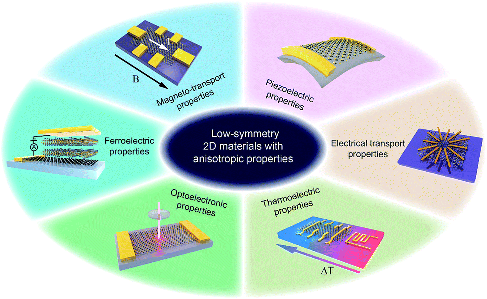 | ||
| Fig. 1 Low-symmetry 2D layered materials with anisotropic electrical transport, magneto-transport, optoelectronic, thermoelectric, piezoelectric, and ferroelectric properties. | ||
2. Crystal structure and electronic band structure
Since materials' anisotropic properties and functionalities are strongly related to their crystal structures and compositions, it is crucial to study the low-symmetry 2D layered crystal structures first. After early investigations on the characterization of structures and properties of bulk samples, the family of low-symmetry 2D layered materials have recently attracted tremendous attentions due to the novel anisotropic properties. Here, we will categorize the low-symmetry 2D layered materials through the conductivity and periodic table of elements as shown in Fig. 2.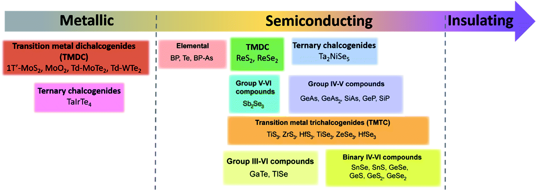 | ||
| Fig. 2 The categorized low-symmetry 2D layered materials by the conductivity and periodic table of elements. | ||
2.1 Elementary 2D material
Among the 2D layered anisotropic materials, black phosphorus (BP) has a wide thickness-tunable direct bandgap (∼0.3 eV of monolayer to 2 eV of bulk) and high intrinsic mobility, with a puckered orthorhombic structure of a Cmca space group symmetry (see Fig. 3), which makes it a promising core material for next-generation (opto)electronic devices.31,62–68 In the atomic layer, each phosphorus atom in BP is connected to three adjacent phosphorus atoms, leading to two distinguishing defined directions: armchair and zigzag directions along the x and y axis, respectively. The highly anisotropic crystal lattice gives rise to its anisotropic in-plane electrical, optical, and phonon properties. Tellurene is another elementary in-plane anisotropic semiconductor, which is comprised of non-covalently bound parallel Te chains. Tellurene crystallizes in a structure composed of Te atomic chains in a triangular helix that are stacked together via van der Waals forces in a hexagonal array. In this structure, Te atoms form covalent bonds only to the two nearest neighboring Te atoms in the helical chain as shown in Fig. 3. The band gap of tellurene is also thickness-tunable varying from nearly direct 0.31 eV (bulk) to indirect 1.17 eV (2 L). Moreover, compared with BP, 2D tellurene also exhibits an extremely high hole mobility (∼105 cm2 V−1 s−1) but has a better environmental stability. Tellurene, therefore, is expected to rival black phosphorus in many applications.15,60,69–74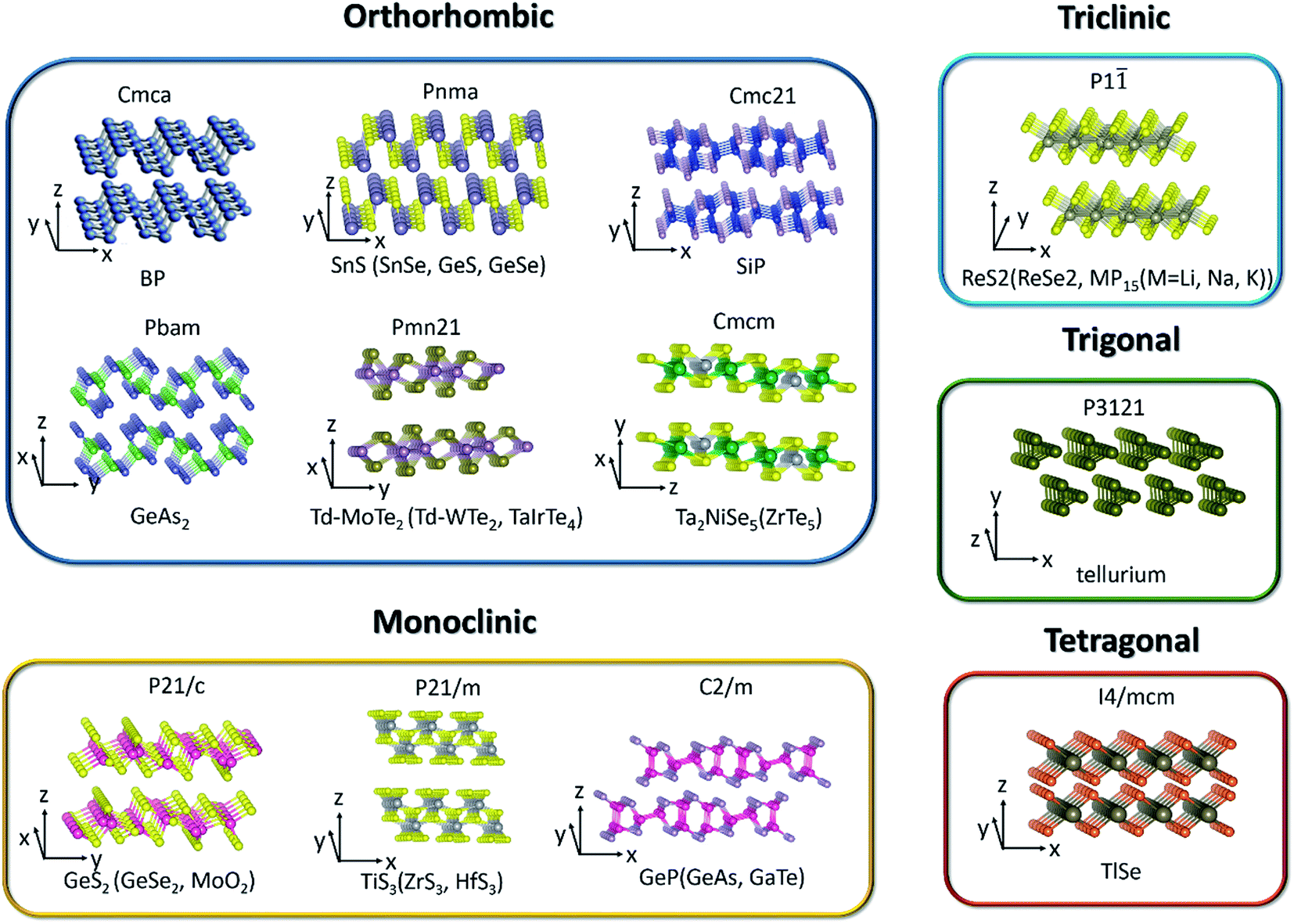 | ||
| Fig. 3 The crystal structure of low-symmetry 2D layered materials. | ||
2.2 Binary IV–VI chalcogenides
Similar to BP, the anisotropic layered IV–VI metal monochalcogenides (MX, M = Ge, Sn; X = S, Se, etc.) also possess puckered orthorhombic (distorted NaCl-type) crystal structure and exhibit high Grüneisen parameters, which give rise to ultralow thermal conductivities and exceptionally high thermoelectric figures of merit.12,75 In addition, their low-symmetry crystal structures can lead to highly anisotropic behaviors manifested in, such as, the in-plane anisotropic carrier's mobility,76–78 photoresponse,42,79–82 and Raman intensity.78,83,84 Conventionally, the zigzag accordion-like projection is defined as x-axis and y-axis denoting the armchair direction. Theoretical calculations have predicted the valley-dependent transport excited by linearly polarized light,85 reversible in-plane anisotropy switching by strain or electric field,86 and anisotropic spin-transport properties.87 Lin et al. demonstrated valley-dependent absorption excited by linearly polarized light.88 Beyond that, in the bulk forms, SnSe and SnS exhibit both multi-valley features at valence bands and very low thermal conductivities, which result in high thermoelectric anisotropic properties.12,75Germanium disulfide (GeS2) and germanium diselenide (GeSe2) are other typical layered materials among binary IV–VI chalcogenides. Monoclinic β-GeSe2 is the most stable phase among all the GeSe2 phases with relatively lower lattice symmetry and exhibits in-plane anisotropic behaviors.56,89,90Fig. 3 shows the crystal structure of GeS2 and β-GeSe2. Unlike BP with strong interlayer coupling, the interlayer interactions of GeS2 and β-GeSe2 are relatively weak.91 Owing to the high stability under ambient environment and large direct bandgap, GeS2 and β-GeSe2 are promising candidates for short-wave photodetection.
2.3 Group IV–V compounds
Group IV–V compounds, silicon and germanium phosphides and arsenides, (e.g., silicon phosphide (SiP), germanium phosphide (GeP), silicon arsenide (SiAs), germanium arsenide (GeAs), and germanium diarsenide (GeAs2)), are another family of low-symmetry layered materials.92–95 It is reported that they are crystallized into different layered structures with either orthorhombic (Cmc21 space group, SiP,44 Pbma space group, SiP2 and GeAs2 (ref. 45)) or monoclinic (C2/m space group, GeP, GeAs and SiAs) symmetries.52,96,97 All these IV–V binary compounds are semiconductors with band gaps of 0.52–1.69 eV. In analogy to the transition metal dichalcogenides, the interactions between the layers are weak.98 People have also investigated the in-plane anisotropic optical, electrical, and optoelectrical properties of them due to the highly anisotropic dispersions of the band structures. Both theoretical calculations and experiments have revealed that 2D SiP has a widely tunable direct band gap (1.69–2.59 eV), high carrier mobility (2.034 × 103 cm2 V−1 s−1) similar to BP and fast photoresponse.44,99,100 Moreover, GeAs and GeAs2 have been proved to be promising in thermoelectric materials by theoretical calculations and experiments.44,99,1002.4 Transition metal dichalcogenides (TMDCs)
TMDCs have attracted increasing research interest due to their attractive physicochemical properties.101–104 Low level of in-plane crystal symmetry can also occur in TMDCs, such as 1T′-molybdenum disulfide (MoS2), Td-molybdenum ditelluride (MoTe2), Td-tungsten ditelluride (WTe2), rhenium disulfide (ReS2), and rhenium diselenide (ReSe2).32,46,48,105,106 Stable metallic 1T′-MoS2 (distorted octahedral MoS2) can be obtained and crystallizes in the orthorhombic crystal structure (Pmn21). Unlike the trigonal prismatic (2H) or octahedral (1T) structure of MoS2, each Mo atom in 1T′-MoS2 is linked with six sulfur atoms and connects with two adjacent Mo atoms.107 Based on the distinct phased-induced anisotropy in 1T′-MoS2, people have investigated its anisotropic electrical transport properties and electrocatalytic performance.46 As for Td-MoTe2 and Td-WTe2, the Td phase shares the same in-plane crystal structure with the 1T′ phase but stacks vertically in a different way as depicted in Fig. 3. Td phase MoTe2 can be regarded as the distortion of MoTe2 along the a-axis. From Fig. 3, we can see that each Mo(W) atom bonds to two adjacent Te atoms, leading to the formation of Mo(W) chains along the a-axis, perpendicular to the in-plane b-axis and the interlayer c-axis. Besides the in-plane anisotropic properties, Td-MoTe2 and Td-WTe2 are also good candidates of type-II Weyl semimetals, which present a large amount of novel physical properties to be undiscovered.Unlike MoS2 with hexagonal structures, group VI TMDCs with rhenium atoms (ReX2, X = S, Se) have distorted CdCl2 layer structure (denoted 1T′ phase, see Fig. 3) leading to triclinic symmetry and large in-plane anisotropy.108,109 In contrast to the 1T phase, the 1T′ phase displays covalent bonding between the nearest Re atoms. The covalent bonded Re atoms form diamond-like pattern leading to quasi one-dimensional Re chains.
2.5 Transition metal trichalcogenides (TMTC)
Group IV transition metal trichalcogenides MX3 are composed of transition metals M belonging to either group IVB (Ti, Zr, Hf) or group VB (Nb, Ta) and chalcogen atoms, X, from group VIA (S, Se, Te).110,111 The MX3 crystal structures (see Fig. 3) can be described as the stacking of individual chain units with the same orientation. Parallel neighbor chains are formed by sequential triangular prisms, where M and X atoms are respectively placed at the corners. These parallel chains in the same quasi-layer are bonded one to another with weak van der Waals interaction. Therefore, each layer of MX3 consists of unique quasi-1D chain-like structure and contributes to its anisotropic properties. In particular, titanium trisulfide (TiS3) that crystallizes in the monoclinic crystal structure (P21/m) with two formula units per unit cell has a direct bandgap of 1.13 eV. Apart from the in-plane electrical anisotropy, TiS3 also exhibits ultrahigh efficiency of visible photoresponse, which makes it a suitable material for polarized photodetectors.112 In addition, NbS3 (triclinic structure), NbSe3 (monoclinic structure), and TaS3 (orthorhombic structure) also present the formation of charge density waves (CDW) and superconductivity at low temperature.113,1142.6 Group III–VI compounds
Layered III–VI semiconductors, such as GaSe and InSe, are of wide interest due to their strong exciton peaks at room temperature absorption edge, large non-linear effect, and high intrinsic carrier mobility.115–117 They open up more possibilities for applications in non-linear optics and electronics. In contrast to GaSe, gallium telluride (GaTe) crystallizes in the monoclinic system with space group (C2/m) and one-third of the Ga–Ga bonds lies in the plane of the layer, as shown in Fig. 3. These bonds are perpendicular to the b-axis and lead to in-plane anisotropic physical properties.Bulk TlSe crystallizes in a tetragonal structure with the space group of I4/mcm. Two thallium ions, monovalent Tl+ and trivalent Tl3+, exist in the crystal-line structure. The trivalent Tl3+ ions form chains of tetrahedral bonds disposed along the tetragonal axis, while the monovalent Tl+ ions are located between the chains and are held together by weak coupling interaction.61
2.7 Ternary transition metal chalcogenides
Nowadays, many 2D ternary transition metal chalcogenides (i.e., Ta2NiS5, TaIrTe4) have been successfully fabricated and are good candidates for excitonic insulator and type II Weyl semimetals.49,118,119 In particular, the crystal structure of bulk Ta2NiS5 is shown in Fig. 3. It crystallizes in the orthorhombic structure with the space group Cmcm. The octahedral coordinated Ta chain and the tetrahedral coordinated Ni chain form one-dimensional structures along the a-axis and stack along the c-axis in the order of Ta–Ni–Ta. The NiS4 and TaS6 units are formed by coordination with the nearest-neighbor S atoms arranged along the c axis with NiS4 units, which are separated by two TaS6 units. Therefore, the different arrangement of chains in the layer gives rise to the one-dimensional characteristic.1202.8 Group V2–VI3 compounds
V2–VI3 compounds, such as Bi2Te3 and Sb2Te3, have gained great interest and extensive research due to their striking thermoelectric properties and possibility to be topological insulators candidates.121,122 Some other V2–VI3 compounds such as Sb2S3, Sb2Se3, and Bi2S3 are composed of one dimensional covalently linked ribbons stacking along the c-axis by weak van der Waals interactions. Take Sb2Se3 for example; bulk Sb2Se3 was recently studied as a light sensitizer in photovoltaic devices due to its narrow direct band gap of about 1.1–1.3 eV, which crystallizes in an orthorhombic structure with the space group Pnma. It consists of staggered, parallel layers of 1D (Sb4Se6)n ribbons that are composed of strong Sb–Se bonds along the 〈001〉 direction. For the 〈100〉 and 〈010〉 directions, the ribbons are stacked owing to their van der Waals interactions.43,1232.9 Others
MoO2 crystallizes in the monoclinic phase with the space group of P21/c and its crystal structure is distorted to the rutile-type.57 This is because O atoms are closely packed into octahedrons and Mo atoms occupy half the space of the octahedral void, which results in the edge-sharing MoO6 octahedrons connected with each other and forms the distorted rutile structure. Although MoO2 has a typical wide band gap, the Mo–Mo metallic bonds give rise to metallic transport properties.124,125The binary alkaline metal phosphide family MP15 (M = Li, Na, K) crystallizes in the triclinic phase with the space group of P.59 It is demonstrated that the anisotropic carrier mobility ratio of single-layer MP15 is extraordinarily large (∼101 to 102) between the x- and y-directions.126 MP15 is composed of parallel units with two antiparallel rows of P tubes in one [P15] unit. In one [P15]-cell, one P atom has two adjacent P atoms and the other 14 P atoms have three adjacent P atoms, which causes a pentagonal arrangement cross-sectionally. This tubular phosphorus structure makes KP15 highly anisotropic.
As seen from Fig. 3, the low-symmetry layered 2D materials in the same crystal structure and space group exhibit similar physical properties, which is highly desirable and important for the analysis of anisotropic properties in low-symmetry layered 2D materials.
3. Fabrication methods
Mono- and few-layer low symmetry 2D materials could be produced by using either “top-down” or “bottom-up” approaches. Top-down approaches include mechanical or ultrasound-assisted liquid phase exfoliation from the single crystal bulk. Bottom-up approaches, whereby the low symmetry materials are grown layer by layer, involve physical vapor deposition (PVD), chemical vapor deposition (CVD), molecular beam epitaxy (MBE), as well as solution synthesis.3.1 Bottom down
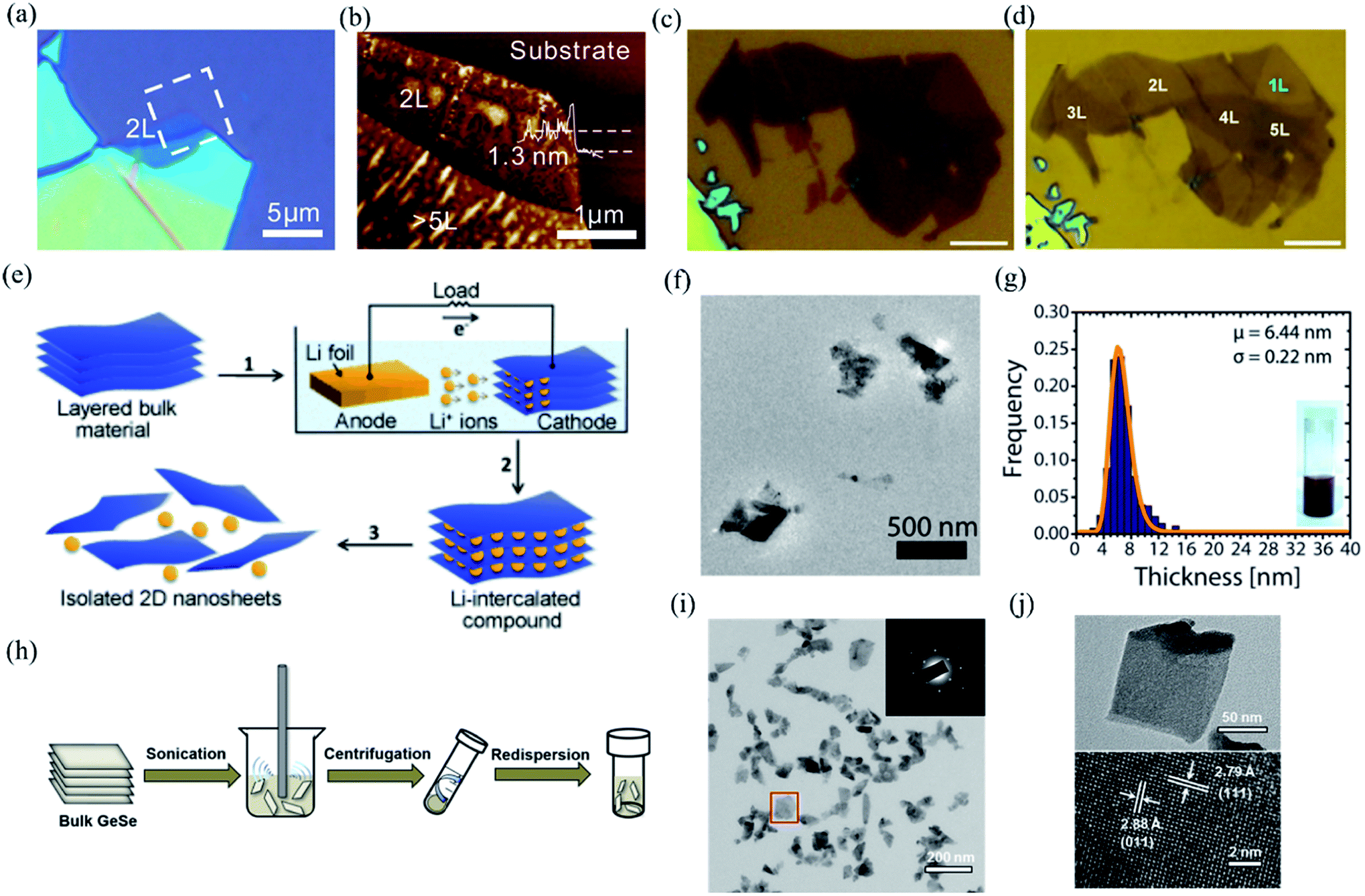 | ||
| Fig. 4 Optical image (a) and AFM image (b) of the mechanical exfoliated BP. Reproduced from ref. 18 with permission from American Chemical Society. (c and d) Optical images of multilayered BP before and after Ar+ plasma thinning. The scale bars are 5 μm. Reproduced from ref. 127 with permission from Tsinghua University Press. (e) Schematic of electrochemical lithiation process for the fabrication of layered 2D nanosheets from bulk material. Reproduced from ref. 128 with permission from Wiley-VCH. (f) Low magnification TEM image of the GeS nanosheets by LPE. (g) Thickness histograms of the as-exfoliated GeS nanosheets. Reproduced from ref. 129 with permission from American Chemical Society. (h) Schematic illustration of the ultrasonic assisted liquid phase exfoliation of GeSe. Large particles after sonication are removed by centrifugation at a moderate speed, while few-layer GeSe dispersed in the supernatant was precipitated at a higher speed and then redispersed in a different solvent. (i) TEM and SAED pattern (inset) of the GeSe nanosheet. (j) TEM and HRTEM image of the dispersed GeSe nanosheet. Reproduced from ref. 132 with permission from American Chemical Society. | ||
3.2 Bottom up
In contrast to bottom down techniques, the bottom up PVD or CVD methods can not only fabricate the 2D layered materials at a large scale and with controllable thickness but also maintain the extraordinary quality, which is desirable for both fundamental research and device applications. For instance, Tian et al. have developed a PVD method, whose schematic instrument is shown in Fig. 5(a), to obtain rhombic SnS nanoplates with different thickness (6–20 nm).137 The AFM image of a 2D SnS nanoplate is shown in Fig. 5(b), which indicates good surface roughness and crystalline degree. Wu et al. recently improved the CVD synthesis of ReS2 monolayers onto [0001] (c-cut) sapphire substrates and produced highly crystallized ReS2 domains with well-defined structural anisotropy (see Fig. 5(c) and (d)).138 As shown in Fig. 5(e), the HRSTEM image of the monolayer ReS2 clearly shows the quasi-1D nature of the synthesized monolayer. The schematic depiction of the lattice directions during the growth of the monolayer is shown in Fig. 5(f). They found that the sapphire substrate can effectively control the shape, thickness, crystallinity, and structural anisotropy of the as-grown ReS2 flakes. Similarly, Zhou et al. have successfully produced single-crystalline rhombic β-GeSe2 flakes using van der Waals epitaxy and a halide precursor, which is shown in Fig. 5(g). The left of Fig. 5(h) shows the crystal structure of β-GeSe2 when looking down the c-axis. The angle between the (110) and (−110) planes is 45°. The unit cell of monoclinic crystalline GeSe2 along the a-axis is shown in the right of Fig. 5(h). It is interesting that the morphology of the flakes, as seen using low magnification (Fig. 5(i)), are consistent with the rhombic features of the molecular structure. Through high-resolution TEM (HRTEM) in Fig. 5(j), the high quality of the GeSe2 rhombic flakes were confirmed with the lattice fringes of the (110) and (021) planes that were measured to be 0.58 and 0.61 nm, respectively.90
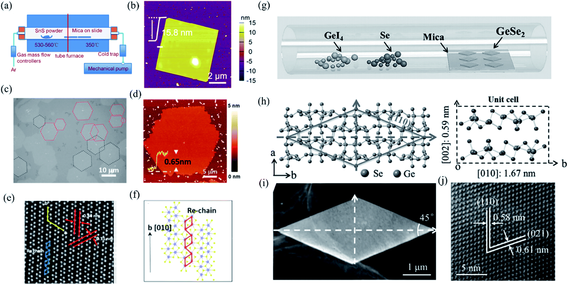 | ||
| Fig. 5 (a) Schematic illustration of the PVD growth system. (b) The AFM image of the as-grown SnS nanoplate transferred onto SiO2 substrates. Reproduced from ref. 137 with permission from American Chemical Society. (c) The optical image of the oriented hexagonal monolayer ReS2 in two distinct directions (red and black dashed lines) grown on the c-cut sapphire substrates by the CVD method. (d) The AFM image of the hexagonal monolayer ReS2. (e) HRSTEM images taken from the ReS2 monolayers showing the quasi-1D nature of the synthesized monolayers and (f) schematic of ReS2 monolayers along the b-axis lattice directions. Reproduced from ref. 138 with permission from American Chemical Society. (g) Schematic of the CVD method for the growth of GeSe2. (h) Crystal structure as determined by XRD. Left: looking down the c-axis, showing the (110) plane system. Right: unit cell of GeSe2, including some lattice parameters. (i) Low-magnification TEM image of the as-grown GeSe2 flake, and (j) the corresponding HRTEM image. Reproduced from ref. 90 with permission from Wiley-VCH. | ||
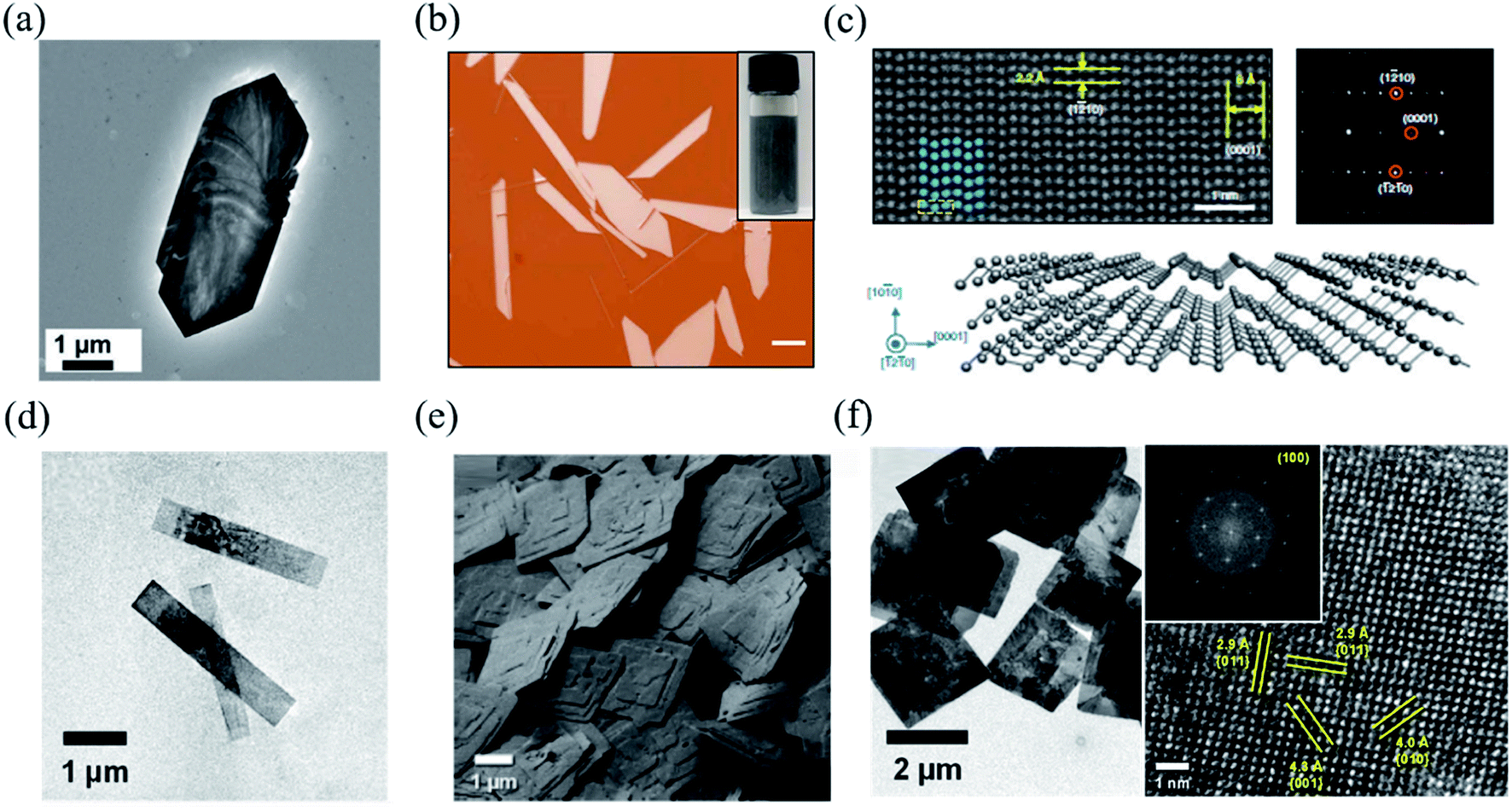 | ||
| Fig. 6 (a) TEM image of a single GeS nanosheet. Reproduced from ref. 142 with permission from Royal Society of Chemistry. (b) The optical image of solution-grown Te flakes. The inset is the optical image of the Te solution dispersion. The scale bar is 20 μm. (c) HAADF-STEM image of tellurene. False-coloured (in blue) atoms are superimposed on the original STEM image to highlight the helical structure. The upper right is the diffraction pattern of tellurene. The bottom is the illustration of the structure of tellurene. Reproduced from ref. 72 with permission from Nature Publishing Group. (d) TEM images of the colloidal SnS nanoribbons. (e) SEM images of the SnS square nanosheets dispersed on a substrate, indicating the high morphological uniformity of individual crystals within the colloidal solution. (f) The left shows the TEM images of μm-scale 2D colloidal SnS square nanosheets. The right is the HRTEM image of a single SnS nanoribbon and (inset) the resulting FFT, both of which reveal that they are single-crystalline with a surface that can be indexed to α-SnS (100). Reproduced from ref. 143 with permission from American Chemical Society. | ||
4. Characterization
The low-symmetry crystal structures and anisotropic band structures of highly asymmetric 2D layered materials enable their strong optical anisotropy. In order to rapidly and directly detect and characterize the optical anisotropy of the low-symmetry 2D layered materials without destroying the samples, the azimuth-dependent reflectance difference microscopy (ADRDM), angle-resolved polarization Raman spectroscopy (ARPRS), and polarization-dependent absorption spectroscopy (PDAS) are effective detection techniques.96,1124.1 Polarization-dependent absorption spectroscopy (PDAS)
The detection principle of PDAS is to directly measure the difference of light absorption, which makes it a reliable method for the identification of crystalline orientation.32,144–146 The scheme of the PDAS measurements is displayed in Fig. 7(a). Firstly, the few-layer 2D materials are exfoliated and transferred on a quartz substrate. Then, the incident light beam is focused onto the flake and the inverted microscope is used to collect the transmitted light. Simultaneously, a spectrometer equipped with a CCD camera can analyze the intensity of transmitted light. If the anisotropic reflection can be neglected, the absorbance (A) is equal to ln(I0/I), where I0 and I are the light intensities transmitted through the quartz substrate nearby the flake location and through the flake, respectively. For example, Li et al. carried out the PRAS measurements of the multilayered GeS flake by rotating the direction of the probe light's polarization from 0° to 180°.145 The anisotropic absorption of GeS is clearly seen in Fig. 7(b) and the polar plot of absorption as a function of degree of polarization is shown in Fig. 7(c), thus presenting the linear dichroic characteristics of GeS. Since the polarization-dependent absorption spectroscopy only considers the electron–photon interaction, it is a reliable way to identify the crystalline orientations. Angle-resolved polarization Raman spectroscopy is another choice besides PDAS. However, it involves both electron–photon and electron–phonon interactions, which makes direct detection of crystalline orientation complicated.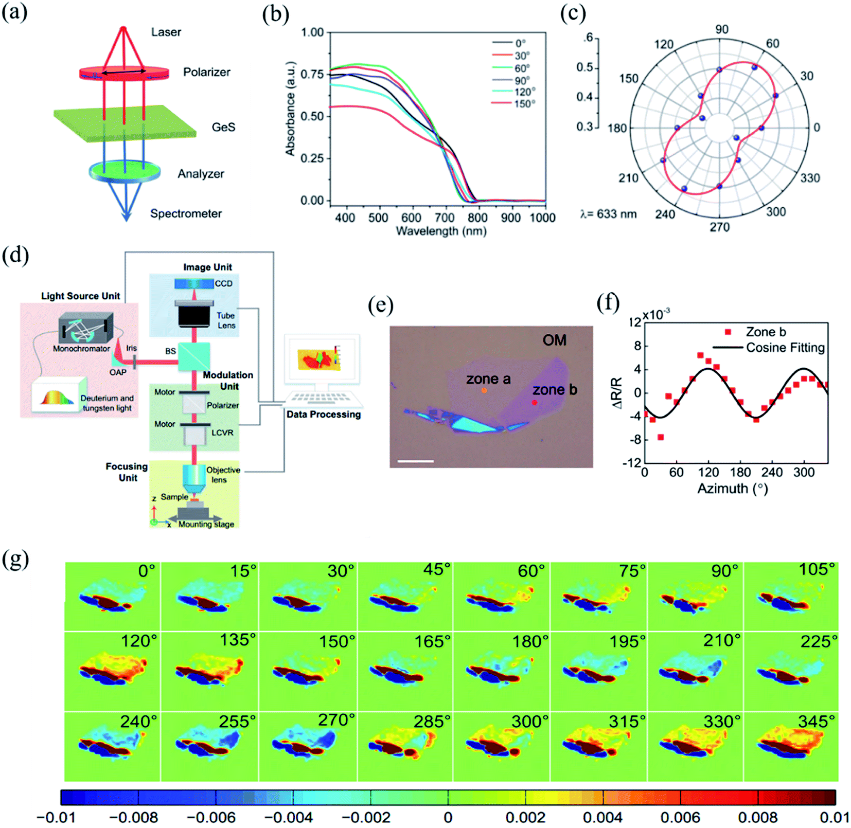 | ||
| Fig. 7 (a) Schematic of PDAS. (b) PDAS of the GeS flake with the spectral range 300–1000 nm. (c) Polar plot of the absorbance of the GeS flake at the wavelength of 633 nm. Reproduced from ref. 145 with permission from American Chemical Society. (d) Scheme of azimuth-dependent reflectance difference microscopy (ADRDM). (e) Optical image of a BP flake on the Si/SiO2 substrate. (f). Azimuth-dependent ΔR/R of zone b. (g) All the azimuth-dependent RDM images. Reproduced from ref. 148 with permission from Royal Society of Chemistry. | ||
4.2 Azimuth-dependent reflectance difference microscopy (ADRDM)
The detection principle of ADRDM is to directly measure the difference in the normalized reflectance (ΔR) between two arbitrary orthogonal directions in the surface plane (a and b) when the sample is illuminated by polarized light, which can be defined as:147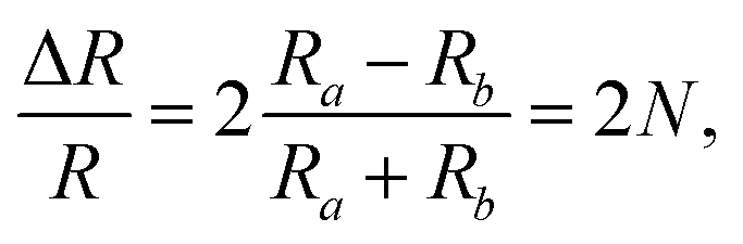 | (1) |
 | (2) |
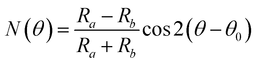
4.3 Angle-resolved polarization Raman spectroscopy (ARPRS)
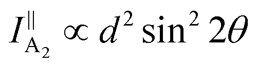
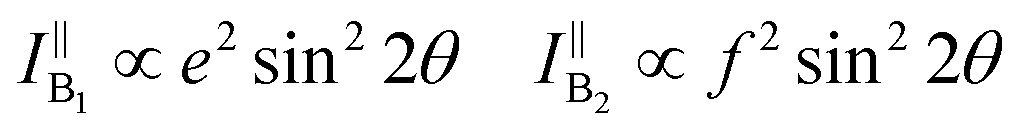
Based on group theory, from Raman tensors and density functional theory (DFT) calculations, the intensity of Raman signals can be quantitatively expressed as:149| I ∝ |eiRes|2 | (3) |
θ, sinθ, 0), where θ is the angle between the incident light polarization and one crystalline orientation of the material. The schematic illustration of the angle-resolved polarized Raman spectroscopy is shown in Fig. 8(a). For the scattered light in the parallel-polarized configuration, es = (cosθ, sinθ, 0), while in the perpendicular-polarized configuration, es = (−sinθ, 0, cosθ). Take TaIrTe4 for example; the Raman tensors of A1, A2, B1, and B2 modes can be expressed as:49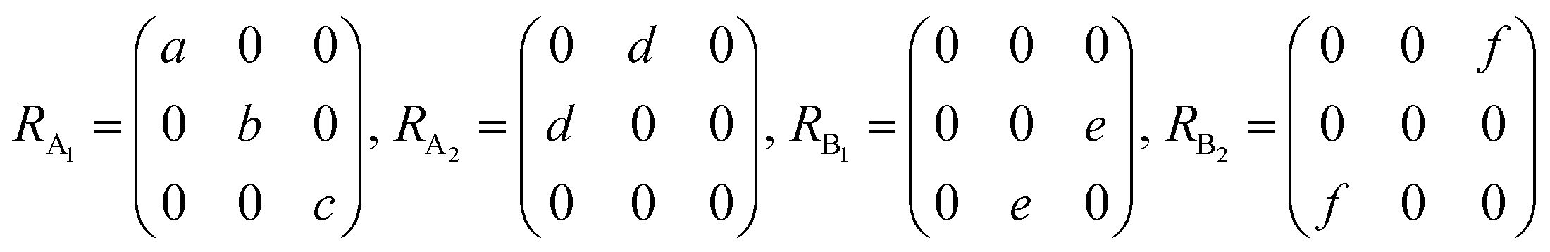 | (4) |
 | (5) |
 | (6) |
 | (7) |
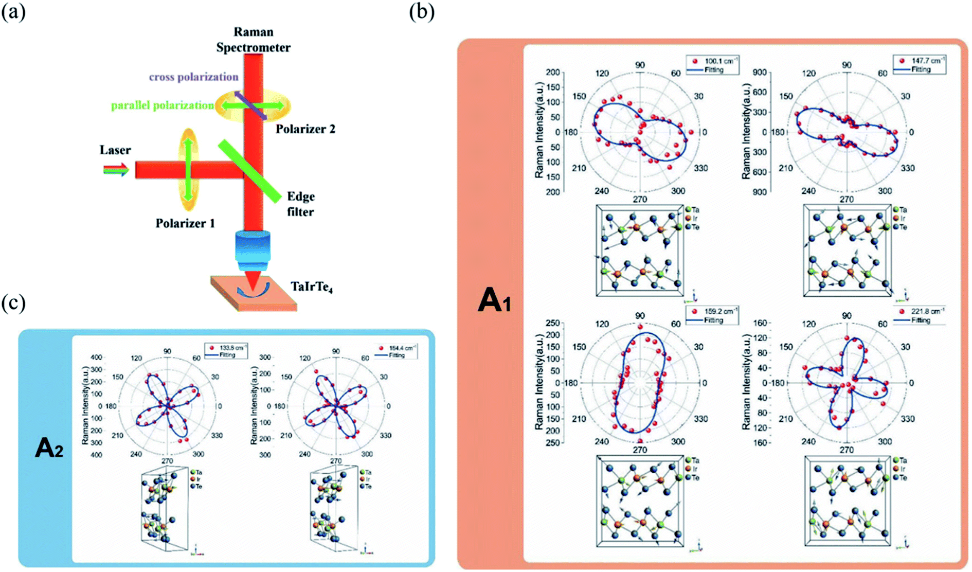 | ||
| Fig. 8 (a) Schematic of the angle-resolved polarized Raman spectroscopy of TaIrTe4 samples. Raman intensities of (b) A1 and (c) A2 modes as a function of the sample rotation angle and the corresponding phonon modes in the atomic view. The scattered dots are the experimental data and the solid lines are the fitting curves. Reproduced from ref. 49 with permission from Wiley-VCH. | ||
From the equations above and the measured Raman intensities of A1 and A2 modes shown in Fig. 7(c) and 8(b), we can see that the intensity of A1 mode varied in periods of 180° and 90° in parallel-polarized configuration, whereas the A2, B1, and B2 modes have 90° variation periods. Therefore, we can deduce the crystalline orientations of the low-symmetry materials by investigating the maximum and minimum intensities of A1 mode with a 180° variation period. The relative magnitude of matrix elements in A1, a > c or a < c determines whether the main axis is along the a-axis or c-axis. However, ARPRS alone cannot confirm the relative magnitude of a and c. In addition, because Raman scattering involves both electron–photon and electron–phonon interactions, the anisotropy of Raman scattering could be diverse at different detection conditions, such as the variable of laser wavelength and the thickness of sample.96 Therefore, combining ARPRS with other techniques such as high resolution TEM (HRTEM), PDAS, ADRDM, or angle-resolved DC conductance is an alternative method to confirm the crystalline orientations.
4.4 Angle-resolved DC conductance
Owing to the highly asymmetric crystal structure, the band dispersions along two perpendicular directions (e.g., Γ–X and Γ–Y) and electron–phonon scattering may be strongly anisotropic. Therefore, the effective mass of the carriers along different crystalline orientations may differ a lot. According to the deformation potential theory, the anisotropy of effective mass gives rise to the anisotropy of the carrier's mobility μ and electrical conductivity σ. Consequently, by using the angle-resolved DC conductance measurement, one can independently determine the crystalline orientations for the low-symmetry layered materials. For instance, the electrical anisotropy of ZrTe5 was determined through the angle-resolved DC conductance measurement.51 In order to eliminate the geometric factors that might affect the current flow, the measured region should be circular. 12 electrodes were patterned uniformly and spaced at an angle of 30° along the directions, as shown in the inset of Fig. 9(a). Fig. 9(a) schematically illustrates the structure of the device. DC conductance measurements across each pair of diagonal electrodes at zero back gate bias were performed and the results are shown in Fig. 9(b). The angle dependent DC conductance fits well with the measured data using the equation:| Gθ = Gxsin2θ + Gycos2θ | (8) |
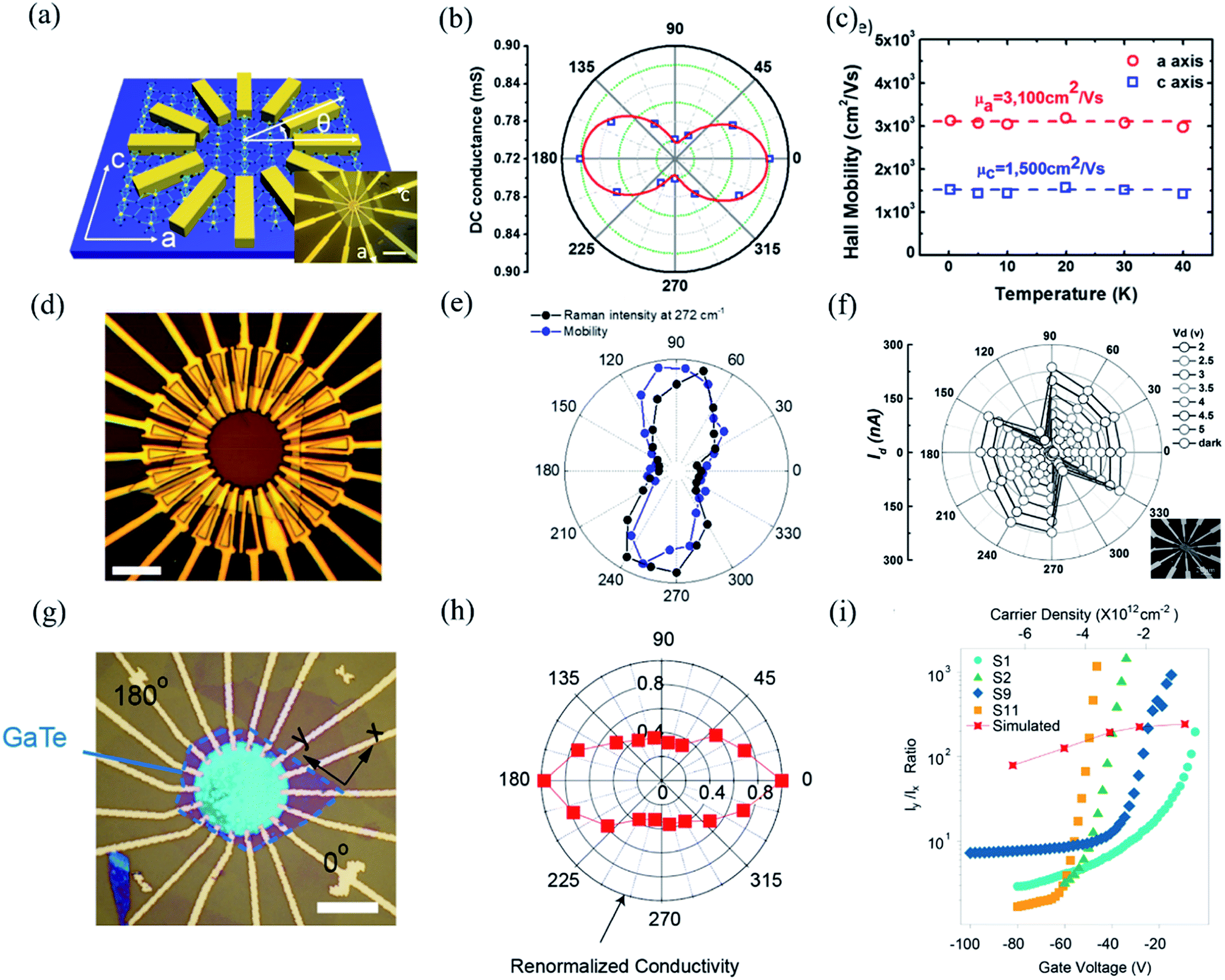 | ||
| Fig. 9 Angle-resolved DC conductance measurements. (a) Schematic illustration of the device structure of ZrTe5 flake. Inset: optical image of this device. Scale bar is 10 μm. (b) Angle-dependent DC conductance of the ZrTe5 flake. The data points are fitted with the equation: σθ = σxsin2θ + σy cos2θ. (c) Hall mobility along a and c axis at low temperatures. Reproduced from ref. 51 with permission from American Chemical Society. (d) Optical image of the transistors on the GeAs flake with electrodes spaced 15° apart for angle-resolved conductance measurement. (e) Polar plot of anisotropic field-effect mobility and Raman intensity at 272 cm−1 with orientation corresponding to optical image in figure (d). Reproduced from ref. 53 with permission from Wiley-VCH. (f) Angle-resolved current of the 10 nm thick Sb2Se3 nanosheet device at bias from 1 to 5 V. The inset is the optical image of the device. Reproduced from ref. 43 with permission from Wiley-VCH. (g) Optical image of a typical device made of 14 nm GaTe flake encapsulated in h-BN with electrodes spaced 20° apart. (h) Polar plot of normalized angle-dependent current at Vds = 2 V and Vg = −80 V. (i) The electrical maximum anisotropic ratio Iy/Ix extracted from different samples as a function of gate voltage. Reproduced from ref. 36 with permission from Nature Publishing Group. | ||
In the same way, Guo et al. also investigated the angle-resolved transport in multi-layered GaAs using the device shown in Fig. 9(d).53 An obvious anisotropic characteristics can be found by the angle dependent field-effect mobility, as shown in Fig. 9(d). The ratio of anisotropic mobility can reach as high as 4.8, which is comparable with black phosphorus and SnSe.78,150 Besides, from Fig. 9(e), we can see that the angle-resolved plot of Raman intensity at 272 cm−1 is very close to that of mobility, which means that the direction of maximum mobility (or conductance) is perpendicular to the b-direction of GeAs. As shown in Fig. 9(f), similar results can also be found in other low-symmetry layered materials such as Sb2Se3, whose ratio between maximum and minimum current is 16, which is the record of the in-plane anisotropic current (or conductance) ratio reported at room temperature.43,54
Recently, Wang et al. discovered that the angle dependent conductance can be effectively modulated by gate bias in few-layered semiconducting GaTe.36 The optical image of the device is shown in Fig. 9(g). By measuring the anisotropic DC conductance at Vg = −80 V, as shown in Fig. 9(h), one can identify that the maximum Ids flow is in 0°, which is parallel to the y-axis, as marked in Fig. 9(g). It is striking that the ratio of anisotropic conductance (Imax/Imin) is gate-tunable and can reach as high as 103 at Vg = −30 V, as shown in Fig. 9(i). The gate-tunable anisotropic conductance is probably due to the different ratio of transmission channels in x- and y-directions at diverse gate bias. By calculating the transmission coefficient, the researchers found that at low gate voltage (−9.1 V), there is almost no x-direction transmission channel in the scattering region between the source energy level and drain energy, while a sizable y-direction transmission is observed, resulting in a large anisotropic ratio at low gate voltages. In contrast, at high gate voltage (−82 V), the transmission is comparable in both x- and y-directions, thus greatly suppressing the anisotropic ratio in GaTe.
Beyond the results described above, researchers have also investigated the anisotropic carrier transport properties of other low-symmetry 2D materials by the angle-resolved DC conductance method as well. The predicted and measured anisotropic effective mass, mobility, and conductance of low-symmetry 2D materials are summarized and depicted in Table 1. We can see that the studies of anisotropic carrier transport properties of certain low-symmetry 2D materials are still missing. There is no doubt that one can fabricate anisotropic devices with higher performance if low-symmetry 2D materials with large anisotropy ratio of carrier transport were studied more deeply.
Based on the detection principles of different measurements mentioned above, we can see that PDAS and ADRDM are reliable ways to quickly and directly identify crystalline orientations without damaging the materials. However, if the 2D materials are extremely thin, the signals of PDAS are too weak to detect and resolve. In addition, the interference effect may cause a reversed result of ADRDM when the 2D materials are placed on a multilayer substrate (e.g., SiO2/Si). ARPRS is another choice besides PDAS and ADRDM. However, it involves both electron–photon and electron–phonon interactions, which make the direct detection of crystalline orientation complicated and difficult. Meanwhile, the anisotropy of Raman scattering is strongly dependent on the laser wavelength and the thickness of the sample. Therefore, ARPRS might be restricted to analysis when it is compared with other techniques. In the end, even though angle-resolved DC conductance measurement can effectively identify the crystal directions, the procedure of fabricating the electrodes is complicated and time consuming.
5. Multifunctionality
5.1 Anisotropic magneto-transport properties
As the first predicted candidate for a type-II Weyl semimetal, Td-WTe2 has become an attractive topic owing to its exotic physical properties, such as huge non-saturated magnetoresistance (MR), chiral anomaly, and ultrahigh carrier mobilities.13,152–154 The non-saturable large MR and chiral anomaly of WTe2 are strongly related to its Td crystal structure. Recently, Li et al. have proved that WTe2 was indeed a type-II Weyl semimetal with topological Fermi arcs by observing the anisotropic chiral anomaly through magneto-transport measurements in one WTe2 nanoribbon.154 When the electric field is applied along the ky(b-)-direction and the magnetic field is applied along the z-(or c-) direction in the b-axis ribbon of WTe2, a closed Weyl orbit is formed (Fig. 10(a)) and corresponds to a trajectory in the xz-plane in real space. The temperature-dependent resistivity curves of the a-axis and b-axis ribbons shown in Fig. 10(b), which demonstrate the anisotropic transport properties in WTe2. A higher residual resistivity along the a-axis than that along the b-axis indicates that the average carrier mobility is smaller along the a-axis than along the b-axis (σ= (n + p)eμ), which is consistent with the transport anisotropy observed previously in bulk WTe2.13,155 In order to confirm the existence of a Weyl orbit (Fermi arcs), the authors measured the MR of both the a-axis and b-axis ribbon at 2 K, as shown in Fig. 10(c), where quantum oscillations can be observed in the b-axis ribbon, while those cannot be seen in the a-axis ribbon. Therefore, it is demonstrated that the quantum oscillations came from the Weyl orbit (Fermi arcs) instead of the trivial surface states. The disappearance of quantum oscillations in the a-axis ribbon can be attributed to the strong mobility anisotropy μa < μb, which is supported by the data in Fig. 10(b). In addition, a negative MR induced by this chiral anomaly should be observed when a magnetic field is applied parallel to the tilted direction of the Weyl cones. Inversely, the positive MR emerges when the unsaturated electric field and the magnetic field are mutually vertical, and the current is parallel to the W-chain.156,157 The anisotropic MR curves measured at 2 K with B∥a, B∥b, and B∥c are shown in Fig. 10(d). Although the magnetic fields are perpendicular to the current in both cases, B∥a and B∥c, the positive MR ratio when B∥a is almost two orders of magnitude smaller than that when B∥c is consistent with a previous observation in bulk WTe2.33
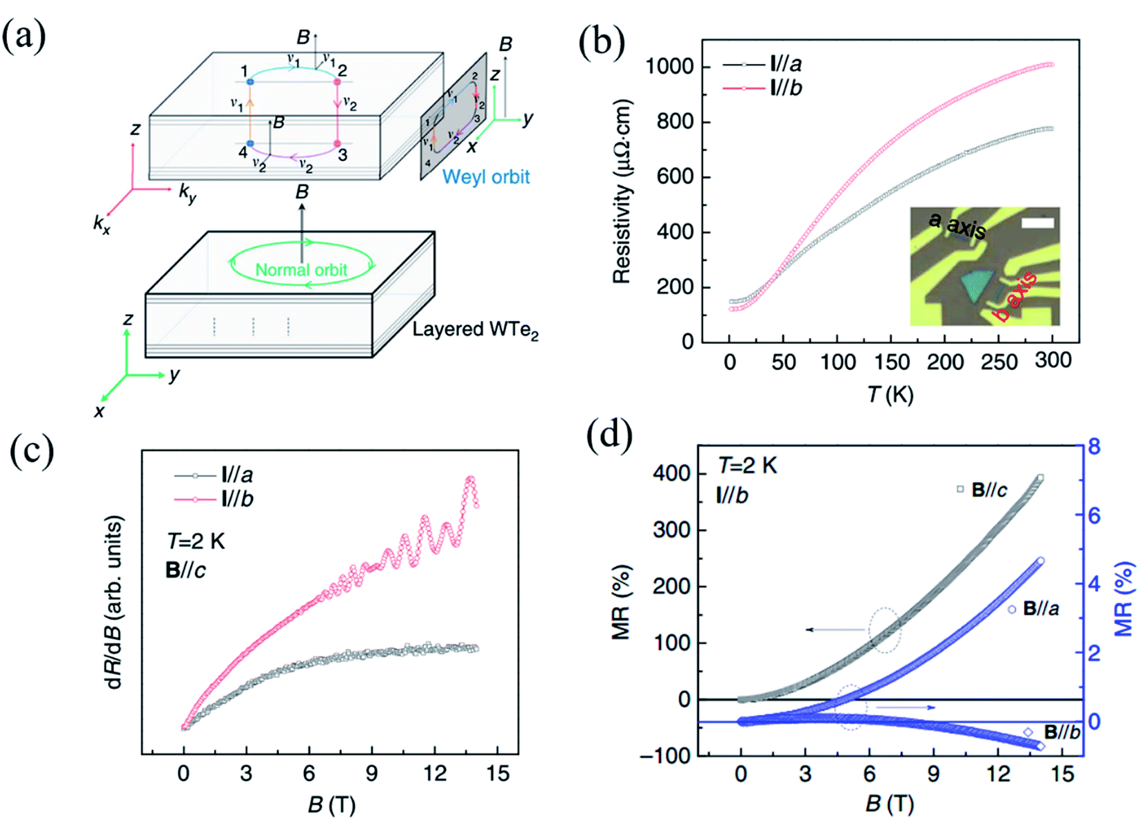 | ||
| Fig. 10 (a) Schematic of a Fermi-arc-induced Weyl orbit in a thin WTe2 nanoribbon, in which the magnetic field is along the z-axis (or c-) axis. The trajectory of the Weyl orbit in real space is in the xz-plane, and the Weyl orbit is plotted in a combination of real space and momentum space. (b) Temperature dependent resistivity of WTe2 nanoribbon with the current along the a- and b-axis. The inset is the optical image of these two ribbons and the scale bar is 5 μm. (c) Quantum oscillation in both the ribbons with the magnetic field parallel to the a- and b-axis. (d) Anisotropic MR data obtained along a, b, and c field directions at 2 K. Reproduced from ref. 154 with permission from Nature Publishing Group. | ||
Meanwhile, negative MR can be observed when B∥b. When magnetic field tilts slightly from the E-field direction, the absolute value of negative MR in the b-axis ribbon decreases quickly, while no negative MR can be observed in the a-axis ribbon. All these experimental data demonstrate that the Weyl points and Fermi arcs are found along the y-direction (b-axis) and are indeed induced by the chiral anomaly. This strongly anisotropic MR behavior is mainly ascribed to the strong anisotropy in the carrier mobility.13,155 Therefore, the measured anisotropic magneto-transport properties can indeed give evidence to the band structure of some low-symmetry 2D materials.
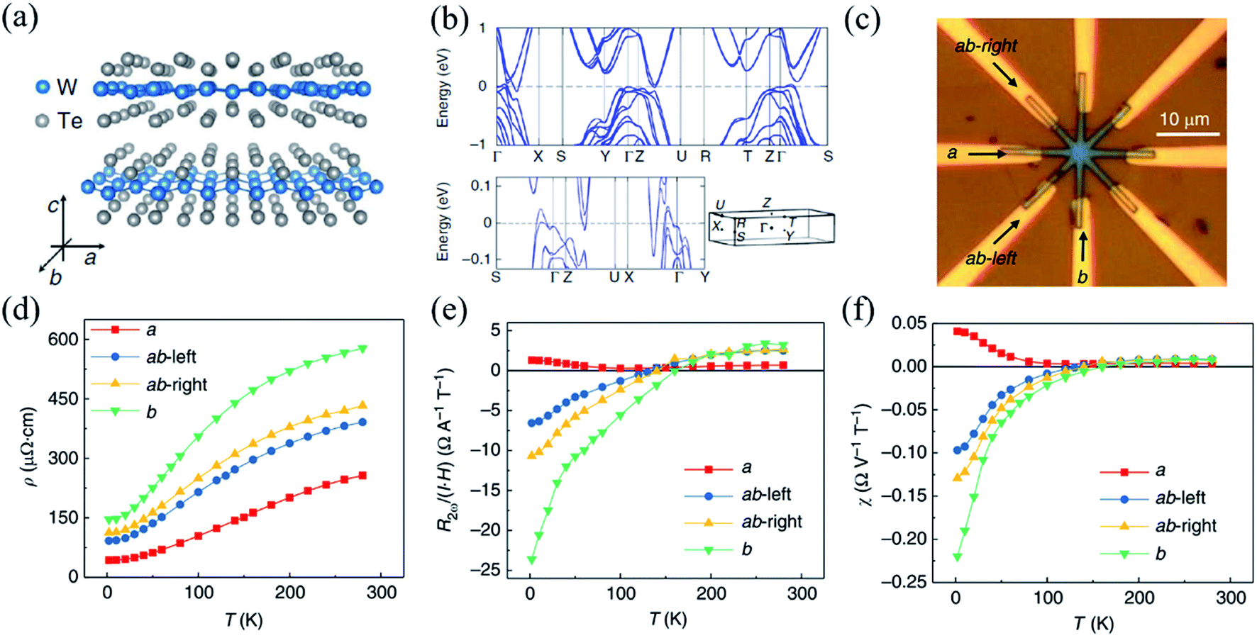 | ||
| Fig. 11 (a) Crystal structure of the layered WTe2 and its crystalline directions. (b) The calculated band structure of bulk WTe2, where the high symmetry k points are indicated in the 3D Brillouin zone sketched underneath. (c) Optical image of the device with arrows indicating the a- and b-directions. (d) Temperature dependent linear resistivity ρ along different crystalline directions. Temperature dependence of NLMR R2ω normalized under unit current and magnetic field (e) and normalized under unit electric voltage and magnetic field (f) along different crystalline orientations. Reproduced from ref. 158 with permission from Nature Publishing Group. | ||
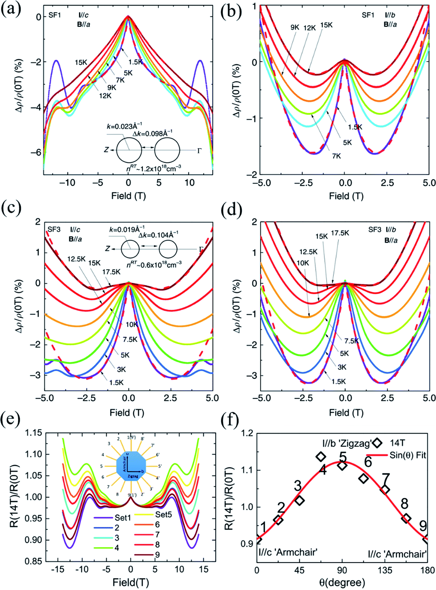 | ||
| Fig. 12 Negative MR in the SF1 sample for (a) I∥c and (b) I∥b at different temperatures, respectively. The low field MR in the SF3 sample at different temperatures when (c) I∥c and (d) I∥b. The low-field negative MR in the SF1 sample is more anisotropic than the SF3 sample. The insets of (a) and (c) show the sketches of the cross-sections of Fermi surfaces for the SF1 and SF3 samples, respectively. (e) Anisotropic MR for I applied along various directions and B∥a. (f) The normalized MR curves by the zero-field resistivity for better comparison. Note the exotic non-saturating behavior up to 14 T for I∥c-axis. Reproduced from ref. 162 with permission from Nature Publishing Group. | ||
However, such exotic behaviors of the I∥c-axis are in striking contrast to the MR behaviors when the current is parallel to the zigzag direction (I∥b-axis). The WL effect induced negative MRs are only dominant at low fields below 2 T before prevalence of positive MR, as shown in Fig. 12(b). However, the MR characteristics in the SF3 sample is less anisotropic than the SF1 sample, while the WL effect is more robust and dominant in the SF3 sample. From Fig. 12(c) and (d), we can see that the SF3 sample shows significantly larger low-field negative MR, which can reach as large as ∼ −3% at 2 T and 1.5 K, than the SF1 sample in the same configuration. But the magnitude of low-field negative MR does not differ much in comparison with the SF1 sample. As shown in the insets of Fig. 12(a) and (c), because the hole doping in the SF1 sample is about two times higher than that of the SF3 sample, the Fermi energy level is shifted downwards by about 5 meV, which reduces the separations between the two pudding-mould valleys. Thus, the momentum mismatch Δp is compensated by the dipole field acceleration of hole carriers and the intervalley scattering is expected to be stronger in SF1 sample when I∥c. Generally, for non-relativistic fermions, the enhanced intervalley scattering gives rise to the suppression of WL because of the interruption of backscattering loops. Therefore, the WL effect induced negative MR is weakened in the SF1 sample and dependent on doping. Also, the in-plane anisotropic WL phenomena may be attributed to strong intervalley scattering along the ferroelectric dipole field direction (c-axis). Moreover, the anisotropic and non-saturating MRs can also be observed in the BR1 sample, as shown in Fig. 12(e) and (f).
 | ||
| Fig. 13 (a) The left is the STEM image of few-layer Td-MoTe2. The right is the simulated STEM images of few-layer MoTe2 in 1T′ and Td stacking viewed along the (001) axis, respectively. (b) MR of the 3 nm-thick MoTe2 device at T = 0.3 K (T = 0.07Tc) with different in-plane tilted angles φ. (c) Angular dependence of the in-plane upper critical field normalized by Pauli limit Hc2/Hp. The experimental data are measured at 0.07Tc, 0.35Tc, 0.6Tc, and 0.95Tc, respectively. The theoretical value of H∥c2 at T = 0 K is plotted to show the two-fold symmetry consistent with the experimental data at low temperature. (d) The left is the first-principle calculations for the band structure of the bilayer Td-MoTe2. The right is the in-plane spin texture at the Fermi level. The temperature phase diagram for the superconducting state with anisotropic SOC under (e) φ = 90° and (f) φ = 0° oriented in-plane magnetic field, respectively. Reproduced from ref. 163 with permission from Nature Publishing Group. | ||
From the reported results above, the anisotropic magneto-transport measurements have been proven to be powerful and useful in the study of band structures and new physical phenomena of low-symmetry layered 2D materials.
5.2 Anisotropic optoelectronic properties
The optoelectronic properties of 2D layered materials are strongly related to the band gap and light absorption coefficient, which are depicted in Table 1. Similar to the conventional semiconductors, low-symmetry 2D materials, e.g., black phosphorus, Td-MoTe2, tellurene, and ternary TaIrTe4, can also realize a wide response range across the electromagnetic spectrum because of their small bandgaps. The bandgap values of low-symmetry 2D materials and their corresponding detection range are summarized in Fig. 14.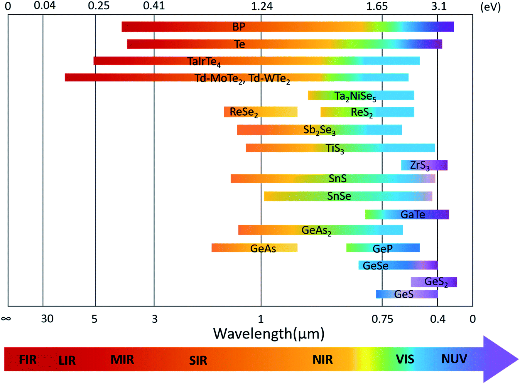 | ||
| Fig. 14 Band-gap values of various low-symmetry 2D materials and their corresponding absorption or detection range. | ||
Likewise, anisotropic optoelectronic properties can be introduced by reducing the lattice symmetry of layered materials. To explore the optoelectronic applications deeply, the detection of polarized light is exceptionally useful in several fields, including optical communication, remote sensing, and optical data storage.166,167 Since highly asymmetric arrangement of atoms can lead to anisotropic band dispersions, further leading to the anisotropic electronic and optical properties, and thus optoelectronic properties, the materials with anisotropic optoelectronic properties are promising candidates for polarization-sensitive photodetectors.31,106,168,169
In order to investigate the anisotropic optoelectronic properties of low-symmetry materials, two-terminal phototransistors were fabricated, as schematically shown in Fig. 15(a).61 In the measurement, the polarized incident light was modulated by the λ/2 plate and changed at a step of one certain degree. Then, the photocurrents at different polarized degrees can be obtained and plotted. Fig. 15(b) shows the typical polarization-sensitive photoresponse of the 2D TlSe flake with two-fold symmetry axes.61 To characterize the magnitude of the linear dichromic photoresponse, a dichroic ratio γ = Imax/Imin can be introduced. The larger the value of the dichroic ratio that is measured, the more sensitivity to the polarized incident light the material exhibits. Furthermore, it is of vital importance to figure out the origin of the polarization-sensitive photoresponse. Zhai et al. have recently measured the polarization-dependent photocurrent of the few-layered GeAs2 at different source-drain bias, as shown in Fig. 15(c).45 The authors also measured the polarization-dependent reflectance contrast of the sample and compared it with the trend of polarization-dependent photocurrent, as shown in Fig. 15(d). Both the photocurrent and reflectance contrast display similar polarization-dependent behavior, which manifests that the origin of polarization-dependent photocurrent is the sample's intrinsic linear dichroism. Javey et al. have investigated the polarization-dependent photoresponse of 2D Te nanoflakes.73 Surprisingly, the behavior of photoresponse as a function of polarization under the illumination of 1.5 and 3 μm laser is different, as shown in Fig. 15(e). Since Te has a direct band gap at 0.71 eV due to a strong absorption when the polarized light is along the direction of Te-chain and an indirect band gap at 0.31 eV owing to a weak absorption when the polarized light is perpendicular to the direction of Te-chain, the photoresponse of 3 μm (indirect band gap) is more anisotropic than that of 1.5 μm (direct band gap). Scanning photocurrent microscopy (SPCM) has been widely utilized for understanding the mechanism for the generation of photocurrent. In order to exclude the anisotropic collection of the photo-induced carriers, Yuan et al. have fabricated a ring-shaped electrode on the BP flake. By measuring the mapping of polarization-dependent photocurrent, they demonstrated that the mechanism of the photocurrent in BP is photothermoelectric effect and the dichroic ratio of BP was about 3.5 at 1200 nm.31 Typical mappings of polarization-dependent photocurrent in a GeAs flake by SPCM measurement are displayed in Fig. 15(f).170 As shown in Fig. 15(f), the photocurrent is predominantly generated near the contact between the electrodes and the sample, and has opposite sign at the two electrodes, from which we can deduce that the Schottky barriers are formed at the interface between the electrodes and the sample, and the mechanism of photocurrent is photovoltaic and photothermoelectric effect. Moreover, from Fig. 15(f), it is clearly seen that the maximum photoresponse direction under 520 nm light is along about 0°, while it differs by about 80° under 830 nm light. This interesting phenomenon may be related to the strongest absorption polarization reversing from b-axis to a-axis at 623 nm. Other low-symmetry layered 2D materials exhibit polarization-sensitive photoresponse as well. We have summarized the reported dichroic ratio of the low-symmetry layered 2D materials in Table 2.
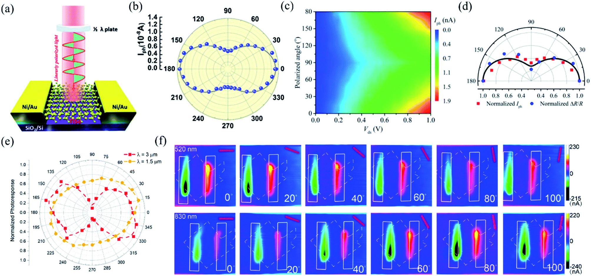 | ||
| Fig. 15 (a) Schematic of the polarization-sensitive photodetector. (b) Polar plots of the photocurrent of the TlSe flake as a function of φ at Vds = 1 V (from 0° to 360° with a step size of 10°). Reproduced from ref. 61 with permission from American Chemical Society. (c) The polarization-dependent photocurrent of GeAs2 at different Vds. The light polarized along the a-axis is defined as 0° reference. (d) Polar plot of the normalized polarization-dependent photocurrent (red square) and reflectance contrast (blue circle) in GeAs2. Reproduced from ref. 45 with permission from Wiley-VCH. (e) Polar plots of the normalized polarization-dependent photocurrent of the 2D Te flake at wavelengths of 3 and 1.5 μm. Reproduced from ref. 73 with permission from American Chemical Society. (f) Polarization-dependent photocurrent mapping of the GeAs device at Vds = 30 mV under the illumination of 520 nm and 830 nm laser, respectively, showing linear dichroic photodetection. Reproduced from ref. 170 with permission from American Chemical Society. | ||
| Device | Responsitivity (R) | Detectivity (D*) | Response time | Dichroic ratio | Ref. |
|---|---|---|---|---|---|
| BP | 518 mA W−1 at 3.4 μm | N/A | N/A | ≈4 at 5 μm | 223 |
| 23A W−1 at 3.68 μm | N/A | N/A | N/A | 224 | |
| 2A W−1 at 4 μm | |||||
| ≈11 A W−1 at 3.7 μm | 6 × 1010 cm Hz1/2 W−1 at 3.8 μm | 12.4 μs (980 nm) | >100 at (3.5 μm) | 217 | |
| As0.83P0.17 | 216.1 mA W−1 at 2.36 μm | 9.2 × 10⁹ jones at 2.4 μm | 0.54 ms at 4.034 μm | 3.88 at (1550 nm) | 225 |
| As0.83P0.17 | 190 mA W−1 at 3.4 μm | N/A | N/A | ≈6 (3.4 μm) | 226 |
| As0.91P0.09 | N/A | 2.4 × 1010 cm Hz1/2 W−1 at 4.2 μm | N/A | N/A | 217 |
| Te | 5.3 A W−1 at 1.5 μm | N/A | N/A | 1.43 (1.5 μm) | 73 |
| 3 A W−1 at 3.0 μm | 6.0 (3.0 μm) | ||||
| GeS | 206 A W−1 at 633 nm | 2.35 × 10¹³ jones at 633 nm | 7 ± 2 ms | N/A | 227 |
| 6.8 × 10³ A at 500 nm | 5.6 × 10¹⁴ jones at 633 nm | 200 ms | N/A | 81 | |
| 173 A W−1 at 405 nm | 1.74 × 10¹³ jones at 633 nm | 0.11 s | N/A | 142 | |
| GeS2 | N/A | N/A | N/A | 2.1 (325 nm) | 228 |
| GeSe | 4.25 A W−1 at 532 nm | N/A | N/A | 1.09 (532 nm), 1.44 (638 nm), 2.16 (808 nm) | 218 |
| 870 A W−1 at 405 nm | 1.12 × 10¹³ jones at 633 nm | 0.15 s | N/A | 142 | |
| 7.05 A W−1 at 633 nm | 3.04 × 10⁸ jones at 633 nm | 1 s | N/A | 79 | |
| 1.6 × 10⁵ A W−1 | 2.9 × 10¹³ jones at 532 nm | N/A | 1.3 (532 nm) | 42 | |
| 43.6−76.3 μA W−1 (UV-Vis) | N/A | 0.2 s | N/A | 229 | |
| β-GeSe2 | N/A | N/A | N/A | 3.4 (450 nm) | 56 |
| 2.5 A W−1 at 450 nm | 1.85 × 10⁸ jones at 450 nm | 0.2 s | N/A | 90 | |
| GeP | 3.11 A W−1 at 532 nm | N/A | N/A | 1.83 (532 nm) | 52 |
| GeAs | 6 A W−1 at 1.6 μm | N/A | 2.5 ms | N/A | |
| N/A | N/A | N/A | 1.49 (520 nm) 4.4 (830 nm) | 170 | |
| o-SiP | 0.05 mA W−1 at 671 nm | N/A | 0.5 s | 3.14 (671 nm) | 44 |
| GeAs2 | N/A | N/A | N/A | ≈2 (532 nm) | 45 |
| GaTe | 274.3 A W−1 | 4 × 10¹² jones at 254 nm | 48 ms | N/A | 19 |
| 104 A W−1 at 532 nm | N/A | 6 ms | N/A | 230 | |
| 0.2 A W−1 | N/A | 2 s | N/A | 231 | |
| TlSe | 1.48 A W−1 at 633 nm | N/A | N/A | 2.65 | 61 |
| SnS | 365 A W−1 at 808 nm | 2.72 × 10⁹ jones at 808 nm | 035 s | 1.49 | 82 |
| 300 A W−1 at 800 nm | 6 × 10⁹ jones at 800 nm | 36 ms | N/A | 232 | |
| 156 A W−1 at 405 nm | 2.94 × 10¹⁰ jones at 405 nm | 5.1 ms | N/A | ||
| 2040 A W−1 | 6 × 10⁹ jones at 800 nm | 90 ms | N/A | ||
| SnSe | N/A | N/A | N/A | 2.15 at 532 nm | 84 |
| 5.5 A W−1 at 370 nm | 6 × 10¹⁰ jones at 370 nm | N/A | N/A | 233 | |
| 330 A W−1 at white light | N/A | N/A | N/A | 234 | |
| TiS3 | 2910 A W−1 | N/A | 4 ms | N/A | 235 |
| 2500 A W−1 at 808 nm | N/A | N/A | ≈4.0 (830 nm) | 169 | |
| ≈4.6 (638 nm) | |||||
| ≈2.8 (532 nm) | |||||
| 5.22 × 10² A W−1 at 1064 nm | 1.69 × 10⁹ jones | 1.53 s | N/A | 236 | |
| Sb2Se3 | 1.58 A W−1 at 633 nm | N/A | N/A | 15.05 at (633 nm) | 43 |
| ReS2 | 4 A W−1 at 633 nm | N/A | 20 μs (633 nm) | N/A | |
| 1000 A W−1 at 532 nm | N/A | 2 s (532 nm) | ≈4 (532 nm) | 32 | |
| 604 A W−1 at 500 nm | 4.44 × 10¹⁰ jones | 2 ms | N/A | 237 | |
| 8.86 × 10⁴ A W−1 at 532 nm | 1.182 × 10¹² jones | 100 s | N/A | 238 | |
| 2.5 × 10⁷ A W−1 at 405 nm | N/A | 0.67 s | N/A | 239 | |
| ReSe2 | 0.1 A W−1 at 633 nm | N/A | 2 ms | ≈2 | 106 |
| 2.98 A W−1 | N/A | 5.47 s | N/A | 240 | |
| 95 A W−1 at 633 nm | N/A | 68 ms | N/A | 58 | |
| Ta2NiSe5 | 17.2 A W−1 at 808 nm | N/A | 3.0 s | N/A | 241 |
| Td-MoTe2 | 0.4 mA W−1 at 532 nm | 1.07 × 10⁸ jones at 532 nm | 42.5 μs (532 nm) 35.8 μs (4 μm), 31.7 μs (10.6 μm) | 2.72 (10.6 μm) 1.92 (4 μm), 1.19 (633 nm) | 47 |
| 4.15 × 10⁻² mA W−1 at 10.6 μm | 9.1 × 10⁶ jones at 10.6 μm | ||||
| Td-WTe2 | 58 A W−1 at 3.8 μm | N/A | 0.018 s (514.5 nm), 0.85 s (3.8 μm), 11.7 s (10.6 μm) | 4.9 (514.5 nm) | 48 |
| Td-TaIrTe4 | 0.34 mA W−1 at 633 nm | 2.7 × 10⁷ jones at 633 nm | 27 μs | 1.13 (633 nm) 1.56 (4 μm), 1.88 (10.6 μm) | 242 |
5.3 Anisotropic thermal conductivity and thermoelectric properties
Thermoelectric (TE) devices can convert heat flow into electrical energy by utilizing the Seebeck effect and the efficiency of thermoelectric conversion is described by the figure of merit, | (9) |
Nowadays, researchers have paid great attention to the investigation of κ of 2D layered materials as well as their anisotropic properties. κ can be measured using micro-Raman method, micro-bridge method, time domain thermo-reflectance (TDTR), and time-resolved magneto-optical Kerr effect (TR-MOKE). In micro-Raman measurements, the suspending samples are transferred onto the micro-fabricated trenches or holes. The laser heats up the samples and creates a temperature gradient in the samples. Meanwhile, by measuring the Raman peak shift with temperature, we can obtain the in-plane thermal conductivity with the help of laser absorption and geometry.171,172 The micro-bridge method was originally used to measure the thermal conductivity of one-dimensional (1D) nanotubes or nanowires.173 Recently, this method has been developed to detect the thermal conductivity of 2D materials.174 The samples are transferred on the two suspended micro-fabricated silicon dioxide membrane islands several microns apart. One of them is the heating membrane and the other one is the sensing membrane. There are two metal resistors under the two suspended islands and a direct current is applied to the metal resistors. Consequently, the current gives rise to a temperature gradient in the sample owing to Joule heating effect. The temperature can be extracted from the resistance change of the sample and thus, we can calculate the thermal conductivity of the sample. The principle of TDTR method is to measure the thermo-reflectance response as a function of delay time between the arrival of the pump and probe pulses on the sample surface. The modulation of the pump beam at rf frequencies is used for lock-in detection of the thermoreflectance signal and to generate useful heat accumulation effects. The in-phase signal from the lock-in outputs Vin is approximately proportional to the temperature difference induced from pump pulse and the out-of-phase signal Vout is approximately proportional to the imaginary part of the temperature oscillations of the pump beam. We calculate the ratio between Vin and Vout voltages,
| R = −Vin/Vout, | (10) |
Recently, many groups have investigated the thermoelectric behaviors of BP. Since the puckered crystal structure of BP results in a lower lattice anharmonicity and larger group velocity along the zigzag direction than the armchair direction, the thermal conductivity (κ) along the armchair direction is several times smaller than that along the zigzag direction, as summarized by Kang et al. in Fig. 16(a).175–178 The difference in the measured in-plane anisotropic thermal conductivity may be related to the different measuring methods and the easily degenerated surface of BP.175,179,180 As seen in Fig. 16(a), the 3D anisotropic thermal conductivities also have thickness dependence in the specific region, which indicates the efficiency of surface or boundary scattering.175 More results have proved that when the vibrations or the propagation directions of phonons are out-of-plane, the scattering is strongly enhanced, which results in the lowest thermal conductivity. But when vibrations and propagation directions of the phonons are in-plane (zigzag or armchair axis), the phonon relaxation time is almost the same. Thus, the phonon relaxation time only contributes to anisotropy in the through-plane thermal conductivity but not the in-plane thermal conductivity.176,180
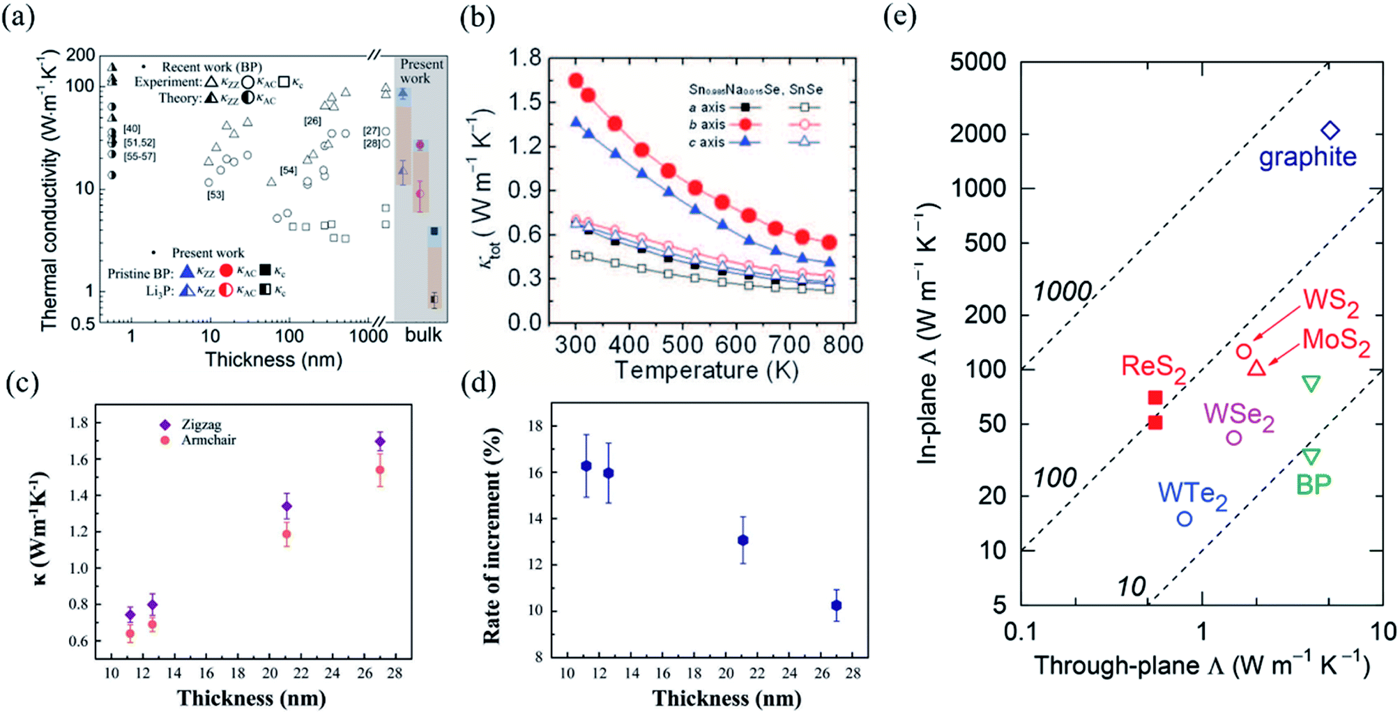 | ||
| Fig. 16 (a) Summarization of thermal conductivity measurement in three different directions plotted in comparison to the reported values as a function of thickness. Thermal conductivities of black phosphorus for the zigzag (blue), the armchair (red), and cross-plane (black) are shown to illustrate the thermal regulation range from the fully charged state (filled symbols) to the fully discharged state (half-filled symbols). Reproduced from ref. 178 with permission from American Chemical Society. (b) Total thermal conductivity as a function of temperature for SnSe crystals. Reproduced from ref. 14 with permission from American Association for the Advancement of Science. (c) The extracted thermal conductivities along the zigzag and armchair directions of Td-WTe2 with different thicknesses. (d) The anisotropic difference in thermal conductivities as a function of sample thickness. Reproduced from ref. 181 with permission from Wiley-VCH. (e) Thermal conductivity of 2D materials whose in-plane and through-plane thermal conductivities in the bulk limit have been experimentally determined at room temperature. The data are taken from graphite,184 MoS2,183 WS2,185 WSe2,186 WTe2,187 and BP.177 The dashed lines represent constant anisotropy ratio (i.e., the in-plane to through-plane thermal conductivity ratio).182 Reproduced from ref. 182 with permission from Wiley-VCH. | ||
Kang et al. have also developed a method to reversibly modify the thermal conductivity of BP by Li ion intercalation. The thermal conductivities of pristine BP and Li3P are found to be highly anisotropic, as shown in Fig. 16(a), which shows that Li ion intercalation covers a remarkably large thermal conductivity tuning range.178 Recently, Zhao et al. have reported that the ZT values of SnSe crystal are extremely high owing to its ultralow lattice thermal conductivity for the distinctive anharmonic structure of SnSe.12,14 Similar to BP, SnSe also has in-plane anisotropic ZT values (2.6 and 2.3 at 950 K along the b and c axes, respectively) and thermal conductivities along different axes as shown in Fig. 16(b).14,178 Strikingly, when SnSe is hole doped with Na, the values of thermal conductivities along three directions are enhanced due to the multiple valence band maxima that lie close together in energy by lifting the Fermi level deep into the band structure. Chen et al. have explored the in-plane anisotropic thermal conductivity of Td-WTe2 flakes with different thickness using micro-Raman spectroscopy method.181 The extracted thermal conductivity of the WTe2 samples with different thickness are shown in Fig. 16(c). Especially for the 11.2 nm thick few-layered WTe2, the thermal conductivity along the zigzag direction, κzigzag = 0.743 W m−1 K−1, is 16.3% larger than that along the armchair direction, κarmchair = 0.639 W m−1 K−1, thus showing a strong anisotropy in the thermal conductivity. But as the thickness of WTe2 increases, the anisotropy of the in-plane thermal conductivity decreases due to the rise of mean free path along the armchair and less phonon-boundary scattering, as shown in Fig. 16(d).
As a typical low-symmetry 2D material, ReS2 also has anisotropic thermal conductivity, which has been studied using the TDTR method by Jang et al.182 They found that the thermal conductivity along the Re-chains was larger than that along the direction transverse to the chains. Apart from that, owing to the weak interlayer coupling in ReS2, the through-plane thermal conductivity is very low (0.55 ± 0.07) W m−1 K−1 compared with other 2D materials such as MoS2 and BP.177,183Fig. 16(e) plots a summary of 2D materials whose in-plane and through-plane thermal conductivities have been experimentally measured in the bulk limit at room temperature. From Fig. 16(e), we can see that the thermal conductivity of ReS2 has a remarkably high anisotropy (130 ± 40 and 90 ± 30) for the two in-plane directions.
It is well known that heavy elements are preferred for thermo-electrical devices with high performance due to the enhanced phonon scattering and lower thermal conductivity.188 Therefore, it has been predicted and experimentally demonstrated that Te is a good candidate as a thermoelectric material due to its high electrical conductivity and low thermal conductivity.69,70,74 Peide D. Ye et al. recently fabricated a state-of-the-art thermoelectric device based on few-layered 2D Te flakes.15 The Seebeck coefficient of few-layered Te can be found to be 413 μV K−1. Then, the thermal conductivity along the 1D chain direction of a similar suspended 2D Te flake is measured by micro-Raman spectroscopy and can be obtained to be about 1.50 W m−1 K−1. Hence, the calculated value of ZT for few-layered Te is about 0.63 at T = 300 K.
Many groups have theoretically predicted that BP has excellent thermoelectric properties.189–191 For example, Zhang et al. calculated and concluded the peak ZT of 1.1 and 0.6 with high electron and hole doping at 800 K.190 However, few reports have been aimed at investigating the TE properties of BP in experiment. Yu Saito et al. have currently measured and successfully tuned the Seebeck coefficient of multilayered BP by gate voltage.192 The maximum of S can reach as high as 510 μV K−1 at 210 K when BP is in the hole-depleted region, which is much higher than the reported bulk single crystal value of 340 μV K−1 at 300 K.189 Zhao et al. have previously proved that single crystals of p-type SnSe exhibited an extremely high ZT of ∼2.6 at 923 K along crystallographic b-direction.12 Lately, n-type Br-doped SnSe single crystals have exhibited a striking ZT of 2.8.193 Other low-symmetric 2D materials with low thermal conductivities and highly anisotropic transport properties also show potential promising thermoelectric applications. Tasuku Sakuma et al. recently measured the thermoelectric power S = −530 μV K−1 and calculated ZT = 0.0023 for quasi-one-dimensional TiS3 microribbon.194
5.4 Ferroelectric and piezoelectric properties
Realizing ferroelectricity and piezoelectricity in 2D layered materials is intriguing for fundamental science and potential applications (e.g., non-volatile memories, generators, and sensors). Ferroelectricity is a characteristic of certain materials that have a spontaneous electric polarization that can be reversed by an external electric field. Up to now, ferroelectricity has been successfully detected in monolayer SnTe, few-layered α-In2Se3, and CuInP2S6 flakes by different methods of measurement.195–199 The ferroelectric behavior usually originates from the breaking of the structural centrosymmetry in the polarization direction. However, there are few reports on achieving ferroelectricity in low-symmetry layered materials, which is extremely impressionable to strain tuning with novel anisotropic properties. Recently, Fei et al. revealed that the unique ionic-potential anharmonicity can induce spontaneous in-plane ferroelectricity in monolayer group-IV monochalcogenides MX (M = Ge, Sn; X = S, Se). They deduced that the ferroelectricity in these materials was robust and their Curie temperatures are all above 300 K. The spontaneous electric polarization is in the order of 10−10 C m−1.200 The monolayer β-GeSe with puckered lattice structure was also predicted to be a 2D ferroelectric material by Guan et al. The in-plane spontaneous electric polarization is about 0.16 nC m−1, which is comparable to that of monolayer SnTe. The intrinsic Curie temperature Tc is calculated to be 212 K by using Monte Carlo simulations.201Fei et al. have also found that two- or three-layer metallic Td-WTe2 exhibits spontaneous out-of-plane electric polarization that can be switched by gate in experiment.202 The authors estimated that the polarization intensity was about 2 × 10⁻⁴ C m−2, which was about three orders of magnitude lower than that of classic ferroelectric BaTiO3.203 Moreover, the researchers also found that the ferroelectric switching characteristics can be effectively tuned by the gate bias. The above observations are practical for ferroelectric applications and may be relevant to novel physical phenomena such as extreme and anisotropic magnetoresistance,37,155 a polar axis, and Weyl points.204,205
Since the ion-displacement of compounds can induce the dipole moment, most of the reported 2D ferroelectric materials are compounds. In comparison, elemental materials are predicted to have no ferroelectricity because there is no electronegativity difference in them. However, Wang et al. recently predicted that 2D few-layered tellurium is a stable ferroelectric material at temperature up to 600 K and the in-plane electric polarization is about 0.16 nC m−1.206 The origin of polarization is the in-plane ion-displacement due to interlayer interactions between the lone-pairs.
Piezoelectric effect is the electric charge accumulated in the material in response to applied mechanical stress and has been used in several devices such as piezoelectric-gated diodes, field effect transistors, and nano-sensors.207 Electric polarization is caused by broken symmetry and exists in most of the non-centrosymmetric materials such as ZnO and Pb(ZrxTi1−x)O3 (PZT).208 Recently, two dimensional piezoelectric materials have attracted tremendous interest because of their good ability to endure enormous strain. It should be noted that there are some materials in which the inversion symmetry can be preserved in the 3D forms but broken in the 2D ones.209,210 For example, bulk MoS2 is not piezoelectric but Wang et al. have proved that the monolayer MoS2 flake can produce a piezoelectric voltage of 15 mV and a current of 20 pA with 0.53% strain.102 For the low-symmetry 2D materials, Fei et al. have predicted that there exists giant anisotropic piezoelectric effects in monolayer group-IV monochalcogenides. By virtue of their unique puckered C2v symmetry and electronic structure, the piezoelectric coefficients of the monolayer group-IV monochalcogenides are surprisingly one to two orders of magnitude larger than other 2D piezoelectric materials such as MoS2, hexagonal BN (h-BN), and GaSe.209,211–213 However, as far as we know, no experimental results have been reported for measuring the piezoelectric voltage or current in monolayer group-IV monochalcogenides. The attempt of exploring anisotropic piezoelectric polarization in low-symmetry 2D materials may offer new possibilities to tailor in-plane anisotropic piezoelectric response in nanotechnology and new accesses for harvesting of energy, which can be further used for self-running nano-devices without using additional energy.
6. Applications
By taking advantage of multifunctionality of low-symmetry 2D layered materials, applications with anisotropic properties can be manufactured. Owing to the ambipolar functionality and high-mobility of BP, Zhu et al. have demonstrated high performance flexible amplitude-modulated (AM) demodulator, ambipolar digital inverter, and frequency doubler.214 The BP AM demodulator is a single-transistor circuit, which can convert RF signal to audio signal. The optical image and schematic of flexible BP AM demodulator are shown in Fig. 17(a) and (b). The FFT output signal spectrum for 100 mV input peak-to-peak carrier amplitude at 100% modulation index is shown in Fig. 17(c) and the authors further demonstrated that the BP AM demodulator worked well. Besides, BP ambipolar digital inverters and a frequency doubler are successfully manufactured based on the ambipolar transport characteristics and high drain current modulation. As shown in Fig. 17(e), a BP push–pull amplifier was fabricated. Two identical bottom gate transistors share the same drain as the output and the bottom gate as the input. The amplified inverted signal with an output/input voltage gain of ∼1.68 can be observed in Fig. 17(e). The frequency doubler is also widely used in analog circuits due to the low energy consumption. Compared to graphene, BP can offer lower power and higher power efficiency because of its lower DC power dissipation and off current. As shown in Fig. 17(f), the BP transistor was biased to realize symmetric transfer characteristic near the minimum conduction point and the output sinusoidal frequency was doubled with a conversion gain of 0.72. Similarly, Liu et al. have also fabricated a digital inverter based on the integration of two separated ReS2 FETs along two orientations, as shown in Fig. 17(d).35 The gain of the inverter is defined as |dVout/dVin| and can reach as high as 4.4 when VDD = 3 V, which is comparable to the MoS2 inverters.215,216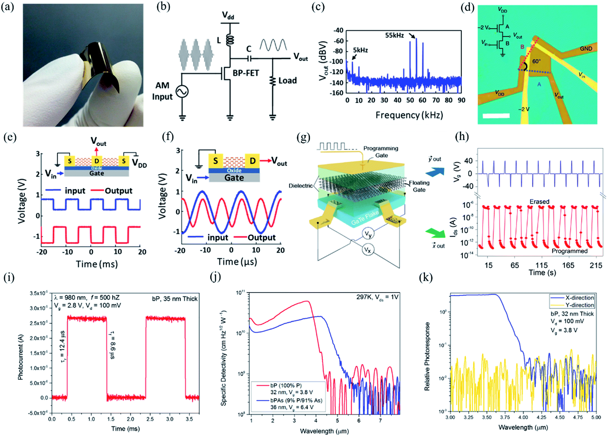 | ||
| Fig. 17 (a) Optical image of few-layer BP devices on a flexible substrate. (b) Schematic of an ideal AM demodulator system based on BP FET operating at the ambipolar point. (c) Output spectrum of the ambipolar transistor demodulator showing the demodulated baseband signal (5 kHz) and the modulated carrier feed-through (55 kHz). Input carrier Vpp = 100 mV. Reproduced from ref. 214 with permission from American Chemical Society. (d) Optical image of a typical inverter device based on few-layer ReS2 flake. The scale bar is 10 mm. The inset is the circuit diagram of the inverter, where the top-gate voltage along the a-axis is fixed at 2 V, the top-gate voltage along the b-axis is the input voltage Vin, and the middle shared electrode is the output voltage Vout. Reproduced from ref. 35 with permission from Nature Publishing Group. (e) The ambipolar digital inverter based on BP at Vg = −0.46 V and Vdd = −2 V. Input pulse oscillates at 100 Hz with peak-to-peak amplitude (Vpp) of 0.5 V. Inverter output pulse showing a gain of about 1.6. (f) Ambipolar single FET frequency doubler based on BP at Vg = 0 V and Vd = −1 V. Input signal is 64 kHz sinusoid with Vpp = 2 V. Output signal oscillates at the double frequency (128 kHz) with a voltage gain of about 0.7. Reproduced from ref. 214 with permission from American Chemical Society. (g) The schematic view of a typical anisotropic memristor based on h-BN/GaTe/h-BN heterojunction with a graphite floating gate. (h) Demonstration of erasing and programming pulses measured in the y-direction. Reproduced from ref. 36 with permission from Nature Publishing Group. (i) Room-temperature temporal photoresponse of a 35 nm-thick BP photoconductor, excited by a 980 nm laser modulated at 50 kHz. (j) Specific detectivity of BP and b-PAs photoconductors with optimized thickness and gate voltage at room temperature.217 (k) Relative response of a BP photoconductor measured for incident light polarized along the x (armchair) and y (zigzag) directions of the BP crystal. Reproduced from ref. 217 with permission from American Chemical Society. | ||
Because of the gate-tunable anisotropic resistance in few-layered GaTe, Wang et al. have manufactured a prototype anisotropic memristor based on GaTe flakes with few-layered graphene as the floating gate.36 The schematic view of the device is shown in Fig. 17(g). Since the anisotropic transport characteristics vary largely in GaTe, the hysteresis memory curves along the x- and y-directions differ a lot, which show a clear window of memory. When the programming gate sweeps from 0 V to −20 V, the device is in the ‘off’ state along both the x- and y-directions. When the erasing gate sweeps from 0 V to 20 V, the device stays in two different ‘on’ states along the x- and y-directions. Therefore, the anisotropic memristor is realized by erasing and programming pulses measured in the y-direction, as shown in Fig. 17(h) and has great potential in direction-sensitive data storage.
Optoelectronic devices rely on light–matter interactions and can convert light into electrical signal or vice versa.218,219 Optoelectronic devices including detectors, lasers LEDs, solar cells, and optical switches are widely used in low-loss optical fiber communications, power generation, and military measure systems. For low dimensional and flexible photodetectors, 2D layered materials should exhibit high responsivity, large detectivity, and fast response time.111,220–222 Unlike graphene, many other 2D layered materials have a band gap and large absorption coefficient, which are beneficent for high performance photodetectors. In addition, polarization-sensitive photodetectors based on low-symmetry layered materials are also desirable in optical communication, remote sensing, and optical data storage.166,167 Apart from the photodetectors based on low-symmetry materials mentioned above, similar polarization-sensitive photodetectors have also been investigated, including wide-band-gap ultraviolet photodetectors (e.g., GeS2), visible-light photodetectors (e.g., ReS2, ReSe2, SnSe, SnS, GeSe, GeS2, GeSe2, GeP, SiP, TiS3, and Sb2Se3), and narrow-band-gap infrared photodetector (e.g., Td-MoTe2, Td-WTe2, and TaIrTe4). For comparison, more performance details of a series of 2D-based polarization-sensitive photodetectors are listed in Table 2. Take the high-performance polarization-sensitive photodetectors based on BP for example.217 As shown in Fig. 17(i) and (j), the photo-response time is ultrafast, which is measured to be about 12.4 μs. The specific detectivity (D*) can be optimized by adjusting the thickness of BP to maximize the absorption and minimize the dark current. The maximum value of D* can reach as high as 6 × 10¹⁰ jones at room temperature, which is about one order of magnitude higher than commercial mid-wave infrared detectors operating at room temperature. As another critical index, the dichroic ratio of photocurrent can be obtained in Fig. 17(k). One can find that the polarization ratio (dichroic ratio) between the two crystal orientations of BP at mid-infrared wavelengths is larger than 100, which is larger than all the other low-symmetry 2D materials. This value is limited by experimental instruments and approaches the extinction ratio of the polarizer used in this study. Since both photo-responsivity and dichroic ratio are the most important indices for the polarization-sensitive photodetectors, here, we have summarized these two values of some low-symmetry 2D materials. As we can see from Fig. 18, both photo-responsivity and dichroic ratios should be high for extraordinary polarization-sensitive photodetectors, which provides guidance for next-generation promising optoelectronic devices with in-plane anisotropy.
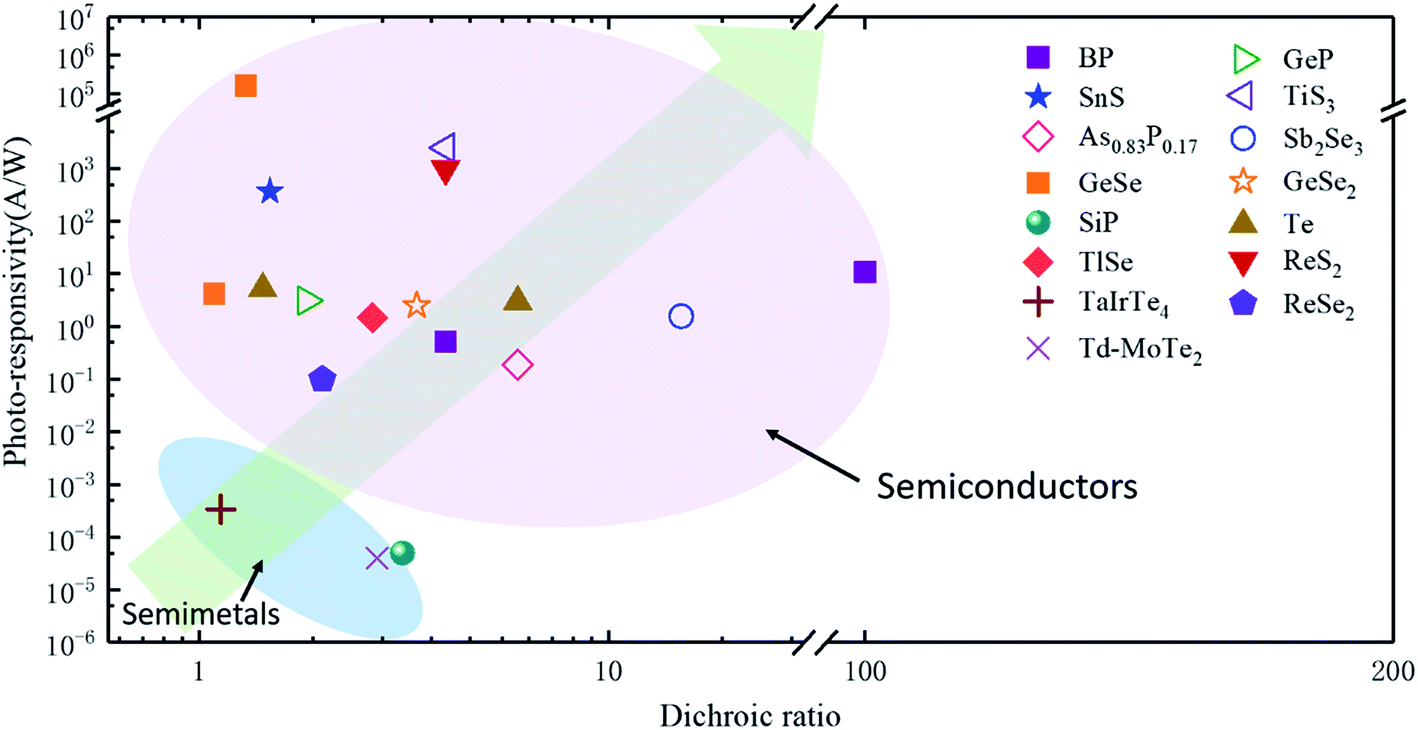 | ||
| Fig. 18 Summarization of the values of photo-responsivity and dichroic ratios for low-symmetry 2D materials. The data are extracted from Table 2. | ||
7. Conclusions and outlook
Here, we have summarized the recent achievements in low-symmetry 2D layered materials and their anisotropic properties, including anisotropic electronic, optoelectronic, magnetic transport, thermoelectric, piezoelectric, and ferroelectric properties, resulting from their anisotropic structures and band structures. On account of the intriguing anisotropic electronic properties, the applications have been fabricated and developed, such as in-plane anisotropic FETs,63,243 anisotropic floating gate memristors,36 digital inverters,35,244 memristors, and polarization-sensitive photodetectors.31,32,45,53,56,228However, there are still many problems to be resolved to attain a comprehensive understanding of the properties of low-symmetry 2D materials and to realize their full potential in multifunctional fields. The potential opportunities and challenges are listed as follows: (1) more work is needed to achieve low-symmetry 2D materials at a large scale. Although a few low-symmetry 2D materials (e.g., SnS and GeSe) have already been manufactured by CVD and PVD methods, still a lot of few-layered low-symmetry 2D materials have only been made by exfoliation, which limits the development of fabrication devices with anisotropic properties. (2) Since the anisotropic ratio of anisotropic 2D materials is still very low (for most of them, it is less than three), exploring new materials and techniques to enhance the in-plane anisotropy of 2D materials is very essential and promising for future anisotropic devices. (3) Searching new methods to effectively modulate and enhance the in-plane anisotropic ratio. Recently, Wang et al. have discovered that the in-plane anisotropic ratio of resistance in few-layered GaTe can be greatly enlarged by tuning the gate voltage.36 But for other low-symmetry 2D materials, whether the gate voltage can also modulate the in-plane anisotropic properties is still unknown. (4) The predicted thermoelectric, piezoelectric, and ferroelectric properties and their anisotropy in some of the low-symmetry 2D materials are still needed to be confirmed and explored by experiments. (5) Although many researchers have deeply investigated the properties of heterostructures based on low-symmetry 2D materials, the isotropic/anisotropic and anisotropic/anisotropic 2D stacked heterostructures require more in-depth study to elucidate the unique properties and upgrade the device performance. (6) Since Wu et al. have predicted that moiré bands of twisted transition metal dichalcogenide homo-bilayers can be topologically non-trivial,245 new physical properties such as quantum spin Hall effect and superconductivity may be observed in twisted bilayer of some particular low-symmetry 2D materials. Overall, the recent findings concerning anisotropic electronics indicate a broad promise in multifunctional applications.
Conflicts of interest
The authors declare no competing financial interests.Acknowledgements
This work is supported by the National Key R&D Program of China (2017YFA0206302) and is supported by the National Natural Science Foundation of China (NSFC) with Grant 11504385, 51627801, 61435010, and 51702219. H. Zhang and Y. Zhang acknowledge the support from the Science and Technology Innovation Commission of Shenzhen (JCYJ20170818093453105, JCYJ20180305125345378). Z. Han acknowledges the support from the Program of State Key Laboratory of Quantum Optics and Quantum Optics Devices (no. KF201816).References
- K. S. Novoselov, A. K. Geim, S. V. Morozov, D. Jiang, Y. Zhang, S. V. Dubonos, I. V. Grigorieva and A. A. Firsov, Science, 2004, 306, 666–669 CrossRef CAS PubMed.
- A. C. Neto, F. Guinea, N. M. Peres, K. S. Novoselov and A. K. Geim, Rev. Mod. Phys., 2009, 81, 109 CrossRef.
- Q. Bao, H. Zhang, Y. Wang, Z. Ni, Y. Yan, Z. X. Shen, K. P. Loh and D. Y. Tang, Adv. Funct. Mater., 2009, 19, 3077–3083 CrossRef CAS.
- H. Zhang, Q. Bao, D. Tang, L. Zhao and K. Loh, Appl. Phys. Lett., 2009, 95, 141103 CrossRef.
- H. Zhang, D. Tang, R. J. Knize, L. Zhao, Q. Bao and K. P. Loh, Appl. Phys. Lett., 2010, 96, 111112 CrossRef.
- Q. Bao, H. Zhang, B. Wang, Z. Ni, C. H. Y. X. Lim, Y. Wang, D. Y. Tang and K. P. Loh, Nat. Photonics, 2011, 5, 411 CrossRef CAS.
- J. Lu, K. Zhang, X. F. Liu, H. Zhang, T. C. Sum, A. H. Castro Neto and K. P. Loh, Nat. Commun., 2013, 4, 2681 CrossRef PubMed.
- T. T. Lv, Y. X. Li, H. F. Ma, Z. Zhu, Z. P. Li, C. Y. Guan, J. H. Shi, H. Zhang and T. J. Cui, Sci. Rep., 2016, 6, 23186 CrossRef CAS PubMed.
- Z. Zhang, Y. Liu, L. Ren, H. Zhang, Z. Huang, X. Qi, X. Wei and J. Zhong, Electrochim. Acta, 2016, 200, 142–151 CrossRef CAS.
- B. Radisavljevic, A. Radenovic, J. Brivio, i. V. Giacometti and A. Kis, Nat. Nanotechnol., 2011, 6, 147 CrossRef CAS PubMed.
- Z. Guo, S. Chen, Z. Wang, Z. Yang, F. Liu, Y. Xu, J. Wang, Y. Yi, H. Zhang, L. Liao, P. K. Chu and X.-F. Yu, Adv. Mater., 2017, 29, 1703811 CrossRef PubMed.
- L. D. Zhao, S. H. Lo, Y. Zhang, H. Sun, G. Tan, C. Uher, C. Wolverton, V. P. Dravid and M. G. Kanatzidis, Nature, 2014, 508, 373–377 CrossRef CAS PubMed.
- Z. Zhu, X. Lin, J. Liu, B. Fauque, Q. Tao, C. Yang, Y. Shi and K. Behnia, Phys. Rev. Lett., 2015, 114, 176601 CrossRef PubMed.
- L. D. Zhao, G. J. Tan, S. Q. Hao, J. Q. He, Y. L. Pei, H. Chi, H. Wang, S. K. Gong, H. B. Xu, V. P. Dravid, C. Uher, G. J. Snyder, C. Wolverton and M. G. Kanatzidis, Science, 2016, 351, 141–144 CrossRef CAS PubMed.
- G. Qiu, S. Huang, M. Segovia, P. K. Venuthurumilli, Y. Wang, W. Wu, X. Xu and P. D. Ye, Nano Lett., 2019, 19, 1955–1962 CrossRef CAS PubMed.
- Y. Chen, C. Zhao, S. Chen, J. Du, P. Tang, G. Jiang, H. Zhang, S. Wen and D. Tang, IEEE J. Sel. Top. Quantum Electron., 2014, 20, 315 Search PubMed.
- Y. Chen, M. Wu, P. Tang, S. Chen, J. Du, G. Jiang, Y. Li, C. Zhao, H. Zhang and S. Wen, Laser Phys. Lett., 2014, 11, 055101 CrossRef.
- S. Zhang, J. Yang, R. Xu, F. Wang, W. Li, M. Ghufran, Y. W. Zhang, Z. Yu, G. Zhang, Q. Qin and Y. Lu, ACS Nano, 2014, 8, 9590–9596 CrossRef CAS PubMed.
- P. Hu, J. Zhang, M. Yoon, X.-F. Qiao, X. Zhang, W. Feng, P. Tan, W. Zheng, J. Liu, X. Wang, J. C. Idrobo, D. B. Geohegan and K. Xiao, Nano Res., 2014, 7, 694–703 CrossRef CAS.
- P. Yan, R. Lin, H. Chen, H. Zhang, A. Liu, H. Yang and S. Ruan, IEEE Photonics Technol. Lett., 2015, 27, 264–267 CAS.
- H. Mu, Z. Wang, J. Yuan, S. Xiao, C. Chen, Y. Chen, Y. Chen, J. Song, Y. Wang, Y. Xue, H. Zhang and Q. Bao, ACS Photonics, 2015, 2, 832–841 CrossRef CAS.
- J. Liu, Y. Chen, P. Tang, C. Xu, C. Zhao, H. Zhang and S. Wen, Opt. Express, 2015, 23, 6418–6427 CrossRef CAS PubMed.
- W. Han, C. Zang, Z. Huang, H. Zhang, L. Ren, X. Qi and J. Zhong, Int. J. Hydrogen Energy, 2014, 39, 19502–19512 CrossRef CAS.
- X. Ren, J. Zhou, X. Qi, Y. Liu, Z. Huang, Z. Li, Y. Ge, S. C. Dhanabalan, J. S. Ponraj, S. Wang, J. Zhong and H. Zhang, Adv. Energy Mater., 2017, 7, 1700396 CrossRef.
- P. Wan, X. Wen, C. Sun, B. K. Chandran, H. Zhang, X. Sun and X. Chen, Small, 2015, 11, 5409–5415 CrossRef CAS PubMed.
- T. Wang, Y. Guo, P. Wan, H. Zhang, X. Chen and X. Sun, Small, 2016, 12, 3748–3756 CrossRef CAS PubMed.
- S. Yang, Y. Liu, W. Chen, W. Jin, J. Zhou, H. Zhang and G. S. Zakharova, Sens. Actuators, B, 2016, 226, 478–485 CrossRef CAS.
- J. Shao, L. Tong, S. Tang, Z. Guo, H. Zhang, P. Li, H. Wang, C. Du and X.-F. Yu, ACS Appl. Mater. Interfaces, 2015, 7, 5391–5399 CrossRef CAS PubMed.
- B. Zhang, F. Lou, R. Zhao, J. He, J. Li, X. Su, J. Ning and K. Yang, Opt. Lett., 2015, 40, 3691–3694 CrossRef CAS PubMed.
- H.-D. Wang, D. K. Sang, Z.-N. Guo, R. Cao, J.-L. Zhao, M. N. U. Shah, T.-J. Fan, D.-Y. Fan and H. Zhang, Chin. Phys. B, 2018, 27, 087308 CrossRef.
- H. Yuan, X. Liu, F. Afshinmanesh, W. Li, G. Xu, J. Sun, B. Lian, A. G. Curto, G. Ye, Y. Hikita, Z. Shen, S. C. Zhang, X. Chen, M. Brongersma, H. Y. Hwang and Y. Cui, Nat. Nanotechnol., 2015, 10, 707–713 CrossRef CAS PubMed.
- F. Liu, S. Zheng, X. He, A. Chaturvedi, J. He, W. L. Chow, T. R. Mion, X. Wang, J. Zhou, Q. Fu, H. J. Fan, B. K. Tay, L. Song, R.-H. He, C. Kloc, P. M. Ajayan and Z. Liu, Adv. Funct. Mater., 2016, 26, 1169–1177 CrossRef CAS.
- C. Tan, P. Yu, Y. Hu, J. Chen, Y. Huang, Y. Cai, Z. Luo, B. Li, Q. Lu, L. Wang, Z. Liu and H. Zhang, J. Am. Chem. Soc., 2015, 137, 10430–10436 CrossRef CAS PubMed.
- H. Tian, Q. Guo, Y. Xie, H. Zhao, C. Li, J. J. Cha, F. Xia and H. Wang, Adv. Mater., 2016, 28, 4991–4997 CrossRef CAS PubMed.
- E. Liu, Y. Fu, Y. Wang, Y. Feng, H. Liu, X. Wan, W. Zhou, B. Wang, L. Shao, C. H. Ho, Y. S. Huang, Z. Cao, L. Wang, A. Li, J. Zeng, F. Song, X. Wang, Y. Shi, H. Yuan, H. Y. Hwang, Y. Cui, F. Miao and D. Xing, Nat. Commun., 2015, 6, 6991 CrossRef CAS PubMed.
- H. Wang, M.-L. Chen, M. Zhu, Y. Wang, B. Dong, X. Sun, X. Zhang, S. Cao, X. Li, J. Huang, L. Zhang, W. Liu, D. Sun, Y. Ye, K. Song, J. Wang, Y. Han, T. Yang, H. Guo, C. Qin, L. Xiao, J. Zhang, J. Chen, Z. Han and Z. Zhang, Nat. Commun., 2019, 10, 2302 CrossRef PubMed.
- M. N. Ali, J. Xiong, S. Flynn, J. Tao, Q. D. Gibson, L. M. Schoop, T. Liang, N. Haldolaarachchige, M. Hirschberger, N. P. Ong and R. J. Cava, Nature, 2014, 514, 205–208 CrossRef CAS PubMed.
- V. C. Kapsalis, J. Phys.: Conf. Ser., 2017, 939, 012026 CrossRef.
- P. Ripka and M. Janosek, IEEE Sens. J., 2010, 10, 1108–1116 Search PubMed.
- A. D. Kent and D. C. Worledge, Nat. Nanotechnol., 2015, 10, 187–191 CrossRef CAS PubMed.
- D. Tan, H. E. Lim, F. Wang, N. B. Mohamed, S. Mouri, W. Zhang, Y. Miyauchi, M. Ohfuchi and K. Matsuda, Nano Res., 2016, 10, 546–555 CrossRef.
- X. Zhou, X. Hu, B. Jin, J. Yu, K. Liu, H. Li and T. Zhai, Adv. Sci., 2018, 5, 1800478 CrossRef PubMed.
- H. Song, T. Li, J. Zhang, Y. Zhou, J. Luo, C. Chen, B. Yang, C. Ge, Y. Wu and J. Tang, Adv. Mater., 2017, 29, 1700441 CrossRef PubMed.
- C. Li, S. Wang, C. Li, T. Yu, N. Jia, J. Qiao, M. Zhu, D. Liu and X. Tao, J. Mater. Chem. C, 2018, 6, 7219–7225 RSC.
- L. Li, P. Gong, D. Sheng, S. Wang, W. Wang, X. Zhu, X. Shi, F. Wang, W. Han, S. Yang, K. Liu, H. Li and T. Zhai, Adv. Mater., 2018, 30, e1804541 CrossRef PubMed.
- G. H. Nam, Q. He, X. Wang, Y. Yu, J. Chen, K. Zhang, Z. Yang, D. Hu, Z. Lai, B. Li, Q. Xiong, Q. Zhang, L. Gu and H. Zhang, Adv. Mater., 2019, 31, e1807764 CrossRef PubMed.
- J. Lai, X. Liu, J. Ma, Q. Wang, K. Zhang, X. Ren, Y. Liu, Q. Gu, X. Zhuo, W. Lu, Y. Wu, Y. Li, J. Feng, S. Zhou, J. H. Chen and D. Sun, Adv. Mater., 2018, 30, e1707152 CrossRef PubMed.
- W. Zhou, J. Chen, H. Gao, T. Hu, S. Ruan, A. Stroppa and W. Ren, Adv. Mater., 2019, 31, e1804629 CrossRef PubMed.
- Y. Liu, Q. Gu, Y. Peng, S. Qi, N. Zhang, Y. Zhang, X. Ma, R. Zhu, L. Tong, J. Feng, Z. Liu and J. H. Chen, Adv. Mater., 2018, 30, e1706402 CrossRef PubMed.
- L. Li, P. Gong, W. Wang, B. Deng, L. Pi, J. Yu, X. Zhou, X. Shi, H. Li and T. Zhai, ACS Nano, 2017, 11, 10264–10272 CrossRef CAS PubMed.
- G. Qiu, Y. Du, A. Charnas, H. Zhou, S. Jin, Z. Luo, D. Y. Zemlyanov, X. Xu, G. J. Cheng and P. D. Ye, Nano Lett., 2016, 16, 7364–7369 CrossRef CAS PubMed.
- L. Li, W. Wang, P. Gong, X. Zhu, B. Deng, X. Shi, G. Gao, H. Li and T. Zhai, Adv. Mater., 2018, 30, e1706771 CrossRef PubMed.
- J. Guo, Y. Liu, Y. Ma, E. Zhu, S. Lee, Z. Lu, Z. Zhao, C. Xu, S. J. Lee, H. Wu, K. Kovnir, Y. Huang and X. Duan, Adv. Mater., 2018, 30, e1705934 CrossRef PubMed.
- J. O. Island, R. Biele, M. Barawi, J. M. Clamagirand, J. R. Ares, C. Sanchez, H. S. van der Zant, I. J. Ferrer, R. D'Agosta and A. Castellanos-Gomez, Sci. Rep., 2016, 6, 22214 CrossRef CAS PubMed.
- A. Pant, E. Torun, B. Chen, S. Bhat, X. Fan, K. Wu, D. P. Wright, F. M. Peeters, E. Soignard, H. Sahin and S. Tongay, Nanoscale, 2016, 8, 16259–16265 RSC.
- Y. Yang, S. C. Liu, W. Yang, Z. Li, Y. Wang, X. Wang, S. Zhang, Y. Zhang, M. Long, G. Zhang, D. J. Xue, J. S. Hu and L. J. Wan, J. Am. Chem. Soc., 2018, 140, 4150–4156 CrossRef CAS PubMed.
- Q. Zheng, P. Ren, Y. Peng, W. Zhou, Y. Yin, H. Wu, W. Gong, W. Wang, D. Tang and B. Zou, J. Phys. Chem. Lett., 2019, 10, 2182–2190 CrossRef CAS PubMed.
- S. Yang, S. Tongay, Y. Li, Q. Yue, J. B. Xia, S. S. Li, J. Li and S. H. Wei, Nanoscale, 2014, 6, 7226–7231 RSC.
- Y. Yang, N. Tian, Y. Zhang, D. Liu, D. Zhang, K. Chang and H. Yan, J. Phys. Chem. Lett., 2018, 9, 732–738 CrossRef CAS PubMed.
- G. Qiu, Y. Wang, Y. Nie, Y. Zheng, K. Cho, W. Wu and P. D. Ye, Nano Lett., 2018, 18, 5760–5767 CrossRef CAS PubMed.
- S. Yang, C. Hu, M. Wu, W. Shen, S. Tongay, K. Wu, B. Wei, Z. Sun, C. Jiang, L. Huang and Z. Wang, ACS Nano, 2018, 12, 8798–8807 CrossRef CAS PubMed.
- L. K. Li, Y. J. Yu, G. J. Ye, Q. Q. Ge, X. D. Ou, H. Wu, D. L. Feng, X. H. Chen and Y. B. Zhang, Nat. Nanotechnol., 2014, 9, 372–377 CrossRef CAS PubMed.
- J. Qiao, X. Kong, Z.-X. Hu, F. Yang and W. Ji, Nat. Commun., 2014, 5, 4475 CrossRef CAS PubMed.
- Z. Guo, H. Zhang, S. Lu, Z. Wang, S. Tang, J. Shao, Z. Sun, H. Xie, H. Wang, X.-F. Yu and P. K. Chu, Adv. Funct. Mater., 2015, 25, 6996–7002 CrossRef CAS.
- Y. Xu, Z. Wang, Z. Guo, H. Huang, Q. Xiao, H. Zhang and X.-F. Yu, Adv. Opt. Mater., 2016, 4, 1223–1229 CrossRef CAS.
- S. Lu, Y. Ge, Z. Sun, Z. Huang, R. Cao, C. Zhao, S. Wen, D. Fan, J. Li and H. Zhang, Photonics Res., 2016, 4, 286–292 CrossRef CAS.
- J. Li, H. Luo, B. Zhai, R. Lu, Z. Guo, H. Zhang and Y. Liu, Sci. Rep., 2016, 6, 30361 CrossRef CAS PubMed.
- L. Kong, Z. Qin, G. Xie, Z. Guo, H. Zhang, P. Yuan and L. Qian, Laser Phys. Lett., 2016, 13, 30361 Search PubMed.
- H. Peng, N. Kioussis and G. J. Snyder, Phys. Rev. B: Condens. Matter Mater. Phys., 2014, 89, 195206 CrossRef.
- S. Lin, W. Li, Z. Chen, J. Shen, B. Ge and Y. Pei, Nat. Commun., 2016, 7, 10287 CrossRef CAS PubMed.
- Z. Xie, C. Xing, W. Huang, T. Fan, Z. Li, J. Zhao, Y. Xiang, Z. Guo, J. Li, Z. Yang, B. Dong, J. Qu, D. Fan and H. Zhang, Adv. Funct. Mater., 2018, 28, 1705833 CrossRef.
- Y. Wang, G. Qiu, R. Wang, S. Huang, Q. Wang, Y. Liu, Y. Du, W. A. Goddard, M. J. Kim, X. Xu, P. D. Ye and W. Wu, Nat. Electron., 2018, 1, 228–236 CrossRef.
- M. Amani, C. Tan, G. Zhang, C. Zhao, J. Bullock, X. Song, H. Kim, V. R. Shrestha, Y. Gao, K. B. Crozier, M. Scott and A. Javey, ACS Nano, 2018, 12, 7253–7263 CrossRef CAS PubMed.
- J. Qiao, Y. Pan, F. Yang, C. Wang, Y. Chai and W. Ji, Sci. Bull., 2018, 63, 159–168 CrossRef CAS.
- W. Shi, M. Gao, J. Wei, J. Gao, C. Fan, E. Ashalley, H. Li and Z. Wang, Adv. Sci., 2018, 5, 1700602 CrossRef PubMed.
- W. C. Yap, Z. Yang, M. Mehboudi, J.-A. Yan, S. Barraza-Lopez and W. Zhu, Nano Res., 2017, 11, 420–430 CrossRef.
- S. Yang, Y. Liu, M. Wu, L.-D. Zhao, Z. Lin, H.-c. Cheng, Y. Wang, C. Jiang, S.-H. Wei, L. Huang, Y. Huang and X. Duan, Nano Res., 2017, 11, 554–564 CrossRef.
- X. Xu, Q. Song, H. Wang, P. Li, K. Zhang, Y. Wang, K. Yuan, Z. Yang, Y. Ye and L. Dai, ACS Appl. Mater. Interfaces, 2017, 9, 12601–12607 CrossRef CAS PubMed.
- J. Liu, Y. Zhou, Y. Lin, M. Li, H. Cai, Y. Liang, M. Liu, Z. Huang, F. Lai, F. Huang and W. Zheng, ACS Appl. Mater. Interfaces, 2019, 11, 4123–4130 CrossRef CAS PubMed.
- Y. Yang, S.-C. Liu, Y. Wang, M. Long, C.-M. Dai, S. Chen, B. Zhang, Z. Sun, Z. Sun, C. Hu, S. Zhang, L. Tong, G. Zhang, D.-J. Xue and J.-S. Hu, Adv. Opt. Mater., 2019, 7, 1801311 CrossRef.
- D. Tan, W. Zhang, X. Wang, S. Koirala, Y. Miyauchi and K. Matsuda, Nanoscale, 2017, 9, 12425–12431 RSC.
- Z. Zhang, J. Yang, K. Zhang, S. Chen, F. Mei and G. Shen, J. Mater. Chem. C, 2017, 5, 11288–11293 RSC.
- C. E. P. Villegas, A. R. Rocha and A. Marini, Phys. Rev. B, 2016, 94, 134306 CrossRef.
- X. Z. Li, J. Xia, L. Wang, Y. Y. Gu, H. Q. Cheng and X. M. Meng, Nanoscale, 2017, 9, 14558–14564 RSC.
- A. S. Rodin, L. C. Gomes, A. Carvalho and A. H. Castro Neto, Phys. Rev. B, 2016, 93, 045431 CrossRef.
- P. Z. Hanakata, A. Carvalho, D. K. Campbell and H. S. Park, Phys. Rev. B, 2016, 94, 035304 CrossRef.
- G. Shi and E. Kioupakis, Nano Lett., 2015, 15, 6926–6931 CrossRef PubMed.
- S. Lin, A. Carvalho, S. Yan, R. Li, S. Kim, A. Rodin, L. Carvalho, E. M. Chan, X. Wang, A. H. Castro Neto and J. Yao, Nat. Commun., 2018, 9, 1455 CrossRef PubMed.
- J. Wang, I. Ronneberger, L. Zhou, L. Lu, V. L. Deringer, B. Zhang, L. Tian, H. Du, C. Jia, X. Qian, M. Wuttig, R. Mazzarello and W. Zhang, Nanoscale, 2018, 10, 7363–7368 RSC.
- X. Zhou, X. Hu, S. Zhou, Q. Zhang, H. Li and T. Zhai, Adv. Funct. Mater., 2017, 27, 1703858 CrossRef.
- Y. Yang, X. Wang, S. C. Liu, Z. Li, Z. Sun, C. Hu, D. J. Xue, G. Zhang and J. S. Hu, Adv. Sci., 2019, 6, 1801810 CrossRef PubMed.
- C. Barreteau, B. Michon, C. Besnard and E. Giannini, J. Cryst. Growth, 2016, 443, 75–80 CrossRef CAS.
- A. Q. Cheng, Z. He, J. Zhao, H. Zeng and R. S. Chen, ACS Appl. Mater. Interfaces, 2018, 10, 5133–5139 CrossRef CAS PubMed.
- B. Mortazavi and T. Rabczuk, Phys. E, 2018, 103, 273–278 CrossRef CAS.
- F. Q. Wang, Y. Guo, Q. Wang, Y. Kawazoe and P. Jena, Chem. Mater., 2017, 29, 9300–9307 CrossRef CAS.
- S. Yang, Y. Yang, M. Wu, C. Hu, W. Shen, Y. Gong, L. Huang, C. Jiang, Y. Zhang and P. M. Ajayan, Adv. Funct. Mater., 2018, 28, 1707379 CrossRef.
- K. Lee, S. Kamali, T. Ericsson, M. Bellard and K. Kovnir, Chem. Mater., 2016, 28, 2776–2785 CrossRef CAS.
- S. Manzeli, D. Ovchinnikov, D. Pasquier, O. V. Yazyev and A. Kis, Nat. Rev. Mater., 2017, 2, 17033 CrossRef CAS.
- S. Zhang, S. Guo, Y. Huang, Z. Zhu, B. Cai, M. Xie, W. Zhou and H. Zeng, 2D Materials, 2016, 4, 015030 CrossRef.
- C. Li, S. Wang, X. Zhang, N. Jia, T. Yu, M. Zhu, D. Liu and X. Tao, CrystEngComm, 2017, 19, 6986–6991 RSC.
- H. Zhang, S. Lu, J. Zheng, J. Du, S. Wen, D. Tang and K. Loh, Opt. Express, 2014, 22, 7249–7260 CrossRef CAS PubMed.
- W. Wu, L. Wang, Y. Li, F. Zhang, L. Lin, S. Niu, D. Chenet, X. Zhang, Y. Hao, T. F. Heinz, J. Hone and Z. L. Wang, Nature, 2014, 514, 470–474 CrossRef CAS PubMed.
- Y. Jiang, L. Miao, G. Jiang, Y. Chen, X. Qi, X.-f. Jiang, H. Zhang and S. Wen, Sci. Rep., 2015, 5, 16372 CrossRef CAS PubMed.
- Z. Li, H. Qiao, Z. Guo, X. Ren, Z. Huang, X. Qi, S. C. Dhanabalan, J. S. Ponraj, D. Zhang, J. Li, J. Zhao, J. Zhong and H. Zhang, Adv. Funct. Mater., 2018, 28, 1705237 CrossRef.
- J. Wang, X. Luo, S. Li, I. Verzhbitskiy, W. Zhao, S. Wang, S. Y. Quek and G. Eda, Adv. Funct. Mater., 2017, 27, 1705237 Search PubMed.
- E. Zhang, P. Wang, Z. Li, H. Wang, C. Song, C. Huang, Z. G. Chen, L. Yang, K. Zhang, S. Lu, W. Wang, S. Liu, H. Fang, X. Zhou, H. Yan, J. Zou, X. Wan, P. Zhou, W. Hu and F. Xiu, ACS Nano, 2016, 10, 8067–8077 CrossRef CAS PubMed.
- Y. Yu, G. H. Nam, Q. He, X. J. Wu, K. Zhang, Z. Yang, J. Chen, Q. Ma, M. Zhao, Z. Liu, F. R. Ran, X. Wang, H. Li, X. Huang, B. Li, Q. Xiong, Q. Zhang, Z. Liu, L. Gu, Y. Du, W. Huang and H. Zhang, Nat. Chem., 2018, 10, 638–643 CrossRef CAS PubMed.
- M. Rahman, K. Davey and S.-Z. Qiao, Adv. Funct. Mater., 2017, 27, 1900040 Search PubMed.
- E. Lorchat, G. Froehlicher and S. Berciaud, ACS Nano, 2016, 10, 2752–2760 CrossRef CAS PubMed.
- Q. Zhao, Y. Guo, Y. Zhou, Z. Yao, Z. Ren, J. Bai and X. Xu, Nanoscale, 2018, 10, 3547–3555 RSC.
- Y. Cui, Z. Zhou, T. Li, K. Wang, J. Li and Z. Wei, Adv. Funct. Mater., 2019, 29, 1900040 CrossRef.
- S. Yang, M. Wu, W. Shen, L. Huang, S. Tongay, K. Wu, B. Wei, Y. Qin, Z. Wang, C. Jiang and C. Hu, ACS Appl. Mater. Interfaces, 2019, 11, 3342–3350 CrossRef CAS.
- S. G. Zybtsev and V. Y. Pokrovskii, Phys. B, 2015, 460, 34–38 CrossRef CAS.
- Z. Z. Wang, P. Monceau, H. Salva, C. Roucau, L. Guemas and A. Meerschaut, Phys. Rev. B: Condens. Matter Mater. Phys., 1989, 40, 11589–11593 CrossRef CAS PubMed.
- C. Wei, X. Chen, D. Li, H. Su, H. He and J. F. Dai, Sci. Rep., 2016, 6, 33890 CrossRef CAS PubMed.
- W. Jie, X. Chen, D. Li, L. Xie, Y. Y. Hui, S. P. Lau, X. Cui and J. Hao, Angew. Chem., Int. Ed. Engl., 2015, 54, 1185–1189 CrossRef CAS PubMed.
- D. A. Bandurin, A. V. Tyurnina, G. L. Yu, A. Mishchenko, V. Zolyomi, S. V. Morozov, R. K. Kumar, R. V. Gorbachev, Z. R. Kudrynskyi, S. Pezzini, Z. D. Kovalyuk, U. Zeitler, K. S. Novoselov, A. Patane, L. Eaves, I. V. Grigorieva, V. I. Fal'ko, A. K. Geim and Y. Cao, Nat. Nanotechnol., 2017, 12, 223–227 CrossRef CAS PubMed.
- K. Sugimoto, S. Nishimoto, T. Kaneko and Y. Ohta, Phys. Rev. Lett., 2018, 120, 247602 CrossRef CAS PubMed.
- K. Mu, H. Chen, Y. Li, Y. Zhang, P. Wang, B. Zhang, Y. Liu, G. Zhang, L. Song and Z. Sun, J. Mater. Chem. C, 2018, 6, 3976–3981 RSC.
- S. A. Sunshine and J. A. Ibers, Inorg. Chem., 1985, 24, 3611–3614 CrossRef CAS.
- P. Ghaemi, R. S. Mong and J. E. Moore, Phys. Rev. Lett., 2010, 105, 166603 CrossRef.
- Y. L. Chen, J. G. Analytis, J. H. Chu, Z. K. Liu, S. K. Mo, X. L. Qi, H. J. Zhang, D. H. Lu, X. Dai, Z. Fang, S. C. Zhang, I. R. Fisher, Z. Hussain and Z. X. Shen, Science, 2009, 325, 178–181 CrossRef CAS PubMed.
- Y. Zhou, L. Wang, S. Chen, S. Qin, X. Liu, J. Chen, D.-J. Xue, M. Luo, Y. Cao, Y. Cheng, E. H. Sargent and J. Tang, Nat. Photonics, 2015, 9, 409–415 CrossRef CAS.
- H. Dai, A. Rath, Y. S. Hearn, S. J. Pennycook and D. H. C. Chua, J. Phys. Chem. Lett., 2018, 9, 7185–7191 CrossRef CAS.
- Q. Zhang, X. Li, Q. Ma, Q. Zhang, H. Bai, W. Yi, J. Liu, J. Han and G. Xi, Nat. Commun., 2017, 8, 14903 CrossRef PubMed.
- N. Tian, Y. Yang, D. Liu, X. Liu, P. H. Tan, D. Zhang, K. Chang, H. Li, M. Zhao, J. R. Li, X. Tang, D. Zhang, Z. Zhang, W. Xiao, H. Yan and Y. Zhang, ACS Nano, 2018, 12, 1712–1719 CrossRef CAS PubMed.
- W. Lu, H. Nan, J. Hong, Y. Chen, C. Zhu, Z. Liang, X. Ma, Z. Ni, C. Jin and Z. Zhang, Nano Res., 2014, 7, 853–859 CrossRef CAS.
- Z. Zeng, Z. Yin, X. Huang, H. Li, Q. He, G. Lu, F. Boey and H. Zhang, Angew. Chem., Int. Ed. Engl., 2011, 50, 11093–11097 CrossRef CAS PubMed.
- D. Lam, K.-S. Chen, J. Kang, X. Liu and M. C. Hersam, Chem. Mater., 2018, 30, 2245–2250 CrossRef CAS.
- P. Zhang, F. Zhao, P. Long, Y. Wang, Y. Yue, X. Liu, Y. Feng, R. Li, W. Hu, Y. Li and W. Feng, Nanoscale, 2018, 10, 15989–15997 RSC.
- Y. Hernandez, V. Nicolosi, M. Lotya, F. M. Blighe, Z. Y. Sun, S. De, I. T. McGovern, B. Holland, M. Byrne, Y. K. Gun'ko, J. J. Boland, P. Niraj, G. Duesberg, S. Krishnamurthy, R. Goodhue, J. Hutchison, V. Scardaci, A. C. Ferrari and J. N. Coleman, Nat. Nanotechnol., 2008, 3, 563–568 CrossRef CAS PubMed.
- Y. Ye, Q. Guo, X. Liu, C. Liu, J. Wang, Y. Liu and J. Qiu, Chem. Mater., 2017, 29, 8361–8368 CrossRef CAS.
- J. Xia, X.-Z. Li, X. Huang, N. Mao, D.-D. Zhu, L. Wang, H. Xu and X.-M. Meng, Nanoscale, 2016, 8, 2063–2070 RSC.
- Z. Y. Cai, B. L. Liu, X. L. Zou and H. M. Cheng, Chem. Rev., 2018, 118, 6091–6133 CrossRef CAS PubMed.
- M.-W. Chen, D. Ovchinnikov, S. Lazar, M. Pizzochero, M. B. Whitwick, A. Surrente, M. Baranowski, O. L. Sanchez, P. Gillet, P. Plochocka, O. V. Yazyev and A. Kis, ACS Nano, 2017, 11, 6355–6361 CrossRef CAS PubMed.
- T. Jurca, M. J. Moody, A. Henning, J. D. Emery, B. H. Wang, J. M. Tan, T. L. Lohr, L. J. Lauhon and T. J. Marks, Angew. Chem., Int. Ed., 2017, 56, 4991–4995 CrossRef CAS PubMed.
- Z. Tian, C. Guo, M. Zhao, R. Li and J. Xue, ACS Nano, 2017, 11, 2219–2226 CrossRef CAS PubMed.
- K. Wu, B. Chen, S. Yang, G. Wang, W. Kong, H. Cai, T. Aoki, E. Soignard, X. Marie, A. Yano, A. Suslu, B. Urbaszek and S. Tongay, Nano Lett., 2016, 16, 5888–5894 CrossRef CAS PubMed.
- J. Song and H. Zeng, Angew. Chem., Int. Ed., 2015, 54, 9760–9774 CrossRef CAS PubMed.
- Z. Liu, Z.-S. Wu, S. Yang, R. Dong, X. Feng and K. Muellen, Adv. Mater., 2016, 28, 2217–2222 CrossRef CAS PubMed.
- Y. W. Zhu, S. Murali, W. W. Cai, X. S. Li, J. W. Suk, J. R. Potts and R. S. Ruoff, Adv. Mater., 2010, 22, 3906–3924 CrossRef CAS PubMed.
- P. Ramasamy, D. Kwak, D.-H. Lim, H.-S. Ra and J.-S. Lee, J. Mater. Chem. C, 2016, 4, 479–485 RSC.
- A. J. Biacchi, S. T. Le, B. G. Alberding, J. A. Hagmann, S. J. Pookpanratana, E. J. Heilweil, C. A. Richter and A. R. Hight Walker, ACS Nano, 2018, 12, 10045–10060 CrossRef CAS PubMed.
- J. Kim, J. U. Lee, J. Lee, H. J. Park, Z. Lee, C. Lee and H. Cheong, Nanoscale, 2015, 7, 18708–18715 RSC.
- Z. Li, Y. Yang, X. Wang, W. Shi, D. J. Xue and J. S. Hu, ACS Appl. Mater. Interfaces, 2019, 11, 24247–24253 CrossRef CAS PubMed.
- H. Yang, H. Jussila, A. Autere, H.-P. Komsa, G. Ye, X. Chen, T. Hasan and Z. Sun, ACS Photonics, 2017, 4, 3023–3030 CrossRef CAS.
- D. S. Martin and P. Weightman, Surf. Interface Anal., 2001, 31, 915–926 CrossRef CAS.
- W. Shen, C. Hu, J. Tao, J. Liu, S. Fan, Y. Wei, C. An, J. Chen, S. Wu, Y. Li, J. Liu, D. Zhang, L. Sun and X. Hu, Nanoscale, 2018, 10, 8329–8337 RSC.
- R. Loudon, J. Phys., 1965, 26, 677–683 CrossRef CAS.
- Y. Liu, T. Low and P. P. Ruden, Phys. Rev. B, 2016, 93, 165402 CrossRef.
- S. Zhao, Y. Wu, K. Zhang, H. Ding, D. Du, J. Zhao, N. Pan and X. J. N. Wang, Nanoscale, 2017, 9, 17610–17616 RSC.
- I. A. Leahy, Y. P. Lin, P. E. Siegfried, A. C. Treglia, J. C. W. Song, R. M. Nandkishore and M. Lee, Proc. Natl. Acad. Sci. U. S. A., 2018, 115, 10570–10575 CrossRef CAS PubMed.
- Y. F. Zhao, H. W. Liu, J. Q. Yan, W. An, J. Liu, X. Zhang, H. C. Wang, Y. Liu, H. Jiang, Q. Li, Y. Wang, X. Z. Li, D. Mandrus, X. C. Xie, M. H. Pan and J. Wang, Phys. Rev. B: Condens. Matter Mater. Phys., 2015, 92, 041104 CrossRef.
- P. Li, Y. Wen, X. He, Q. Zhang, C. Xia, Z. M. Yu, S. A. Yang, Z. Zhu, H. N. Alshareef and X. X. Zhang, Nat. Commun., 2017, 8, 2150 CrossRef PubMed.
- Y. Zhao, H. Liu, J. Yan, W. An, J. Liu, X. Zhang, H. Wang, Y. Liu, H. Jiang, Q. Li, Y. Wang, X.-Z. Li, D. Mandrus, X. C. Xie, M. Pan and J. Wang, Phys. Rev. B: Condens. Matter Mater. Phys., 2015, 92, 041104 CrossRef.
- E. Zhang, R. Chen, C. Huang, J. Yu, K. Zhang, W. Wang, S. Liu, J. Ling, X. Wan, H. Z. Lu and F. Xiu, Nano Lett., 2017, 17, 878–885 CrossRef CAS PubMed.
- Y. Wang, E. Liu, H. Liu, Y. Pan, L. Zhang, J. Zeng, Y. Fu, M. Wang, K. Xu, Z. Huang, Z. Wang, H. Z. Lu, D. Xing, B. Wang, X. Wan and F. Miao, Nat. Commun., 2016, 7, 13142 CrossRef CAS PubMed.
- P. He, C.-H. Hsu, S. Shi, K. Cai, J. Wang, Q. Wang, G. Eda, H. Lin, V. M. Pereira and H. Yang, Nat. Commun., 2019, 10, 866 CrossRef.
- T. Yokouchi, N. Kanazawa, A. Kikkawa, D. Morikawa, K. Shibata, T. Arima, Y. Taguchi, F. Kagawa and Y. Tokura, Nat. Commun., 2017, 8, 866 CrossRef CAS PubMed.
- R. Wakatsuki and N. Nagaosa, Phys. Rev. Lett., 2018, 121, 026601 CrossRef CAS PubMed.
- P. He, S. S. L. Zhang, D. Zhu, Y. Liu, Y. Wang, J. Yu, G. Vignale and H. Yang, Nat. Phys., 2018, 14, 495–499 Search PubMed.
- Z. Wang, C. Fan, Z. Shen, C. Hua, Q. Hu, F. Sheng, Y. Lu, H. Fang, Z. Qiu, J. Lu, Z. Liu, W. Liu, Y. Huang, Z. A. Xu, D. W. Shen and Y. Zheng, Nat. Commun., 2018, 9, 47 Search PubMed.
- J. Cui, P. Li, J. Zhou, W. Y. He, X. Huang, J. Yi, J. Fan, Z. Ji, X. Jing, F. Qu, Z. G. Cheng, C. Yang, L. Lu, K. Suenaga, J. Liu, K. T. Law, J. Lin, Z. Liu and G. Liu, Nat. Commun., 2019, 10, 2044 Search PubMed.
- A. Kormányos, V. Zólyomi, N. D. Drummond, P. Rakyta, G. Burkard and V. I. Fal'ko, Phys. Rev. B: Condens. Matter Mater. Phys., 2013, 88, 045416 CrossRef.
- J. M. Lu, O. Zheliuk, I. Leermakers, N. F. Q. Yuan, U. Zeitler, K. T. Law and J. T. Ye, Science, 2015, 350, 1353–1357 CrossRef CAS PubMed.
- W.-C. Kim, N.-C. Park, Y.-J. Yoon, H. Choi and Y.-P. Park, Opt. Rev., 2007, 14, 236–242 CrossRef CAS.
- J. S. Tyo, D. L. Goldstein, D. B. Chenault and J. A. Shaw, Appl. Opt., 2006, 45, 5453–5469 CrossRef PubMed.
- S. Zhao, J. Wu, K. Jin, H. Ding, T. Li, C. Wu, N. Pan and X. Wang, Adv. Funct. Mater., 2018, 28, 1802011 CrossRef.
- S. Liu, W. Xiao, M. Zhong, L. Pan, X. Wang, H. X. Deng, J. Liu, J. Li and Z. Wei, Nanotechnology, 2018, 29, 184002 CrossRef PubMed.
- Z. Zhou, M. Long, L. Pan, X. Wang, M. Zhong, M. Blei, J. Wang, J. Fang, S. Tongay, W. Hu, J. Li and Z. Wei, ACS Nano, 2018, 12, 12416–12423 CrossRef CAS PubMed.
- Z. Luo, J. Tian, S. Huang, M. Srinivasan, J. Maassen, Y. P. Chen and X. Xu, ACS Nano, 2018, 12, 1120–1127 CrossRef CAS PubMed.
- T. Kodama, M. Ohnishi, W. Park, T. Shiga, J. Park, T. Shimada, H. Shinohara, J. Shiomi and K. E. Goodson, Nat. Mater., 2017, 16, 892–897 CrossRef CAS PubMed.
- P. Kim, L. Shi, A. Majumdar and P. L. McEuen, Phys. Rev. Lett., 2001, 87, 215502 CrossRef CAS PubMed.
- M. T. Pettes, I. Jo, Z. Yao and L. Shi, Nano Lett., 2011, 11, 1195–1200 CrossRef CAS PubMed.
- S. Lee, F. Yang, J. Suh, S. Yang, Y. Lee, G. Li, H. Sung Choe, A. Suslu, Y. Chen, C. Ko, J. Park, K. Liu, J. Li, K. Hippalgaonkar, J. J. Urban, S. Tongay and J. Wu, Nat. Commun., 2015, 6, 8573 CrossRef CAS PubMed.
- Z. Luo, J. Maassen, Y. Deng, Y. Du, R. P. Garrelts, M. S. Lundstrom, P. D. Ye and X. Xu, Nat. Commun., 2015, 6, 8572 CrossRef CAS PubMed.
- H. Jang, J. D. Wood, C. R. Ryder, M. C. Hersam and D. G. Cahill, Adv. Mater., 2015, 27, 8017–8022 CrossRef CAS PubMed.
- J. S. Kang, M. Ke and Y. Hu, Nano Lett., 2017, 17, 1431–1438 CrossRef CAS PubMed.
- B. Sun, X. Gu, Q. Zeng, X. Huang, Y. Yan, Z. Liu, R. Yang and Y. K. Koh, Adv. Mater., 2017, 29, 1603297 CrossRef PubMed.
- B. Smith, B. Vermeersch, J. Carrete, E. Ou, J. Kim, N. Mingo, D. Akinwande and L. Shi, Adv. Mater., 2017, 29, 1603756 CrossRef PubMed.
- Y. Chen, B. Peng, C. Cong, J. Shang, L. Wu, W. Yang, J. Zhou, P. Yu, H. Zhang, Y. Wang, C. Zou, J. Zhang, S. Liu, Q. Xiong, H. Shao, Z. Liu, H. Zhang, W. Huang and T. Yu, Adv. Mater., 2019, 31, e1804979 CrossRef PubMed.
- H. Jang, C. R. Ryder, J. D. Wood, M. C. Hersam and D. G. Cahill, Adv. Mater., 2017, 29, 1700650 CrossRef.
- J. Liu, G.-M. Choi and D. G. Cahill, J. Appl. Phys., 2014, 116, 233107 CrossRef.
- J. P. Feser and D. G. Cahill, Rev. Sci. Instrum., 2013, 84, 049901 CrossRef.
- A. Pisoni, J. Jacimovic, R. Gaal, B. Nafradi, H. Berger, Z. Revay and L. Forro, Scr. Mater., 2016, 114, 48–50 CrossRef CAS.
- C. Chiritescu, D. G. Cahill, N. Nguyen, D. Johnson, A. Bodapati, P. Keblinski and P. Zschack, Science, 2007, 315, 351–353 CrossRef CAS PubMed.
- Y. Zhou, H. Jang, J. M. Woods, Y. Xie, P. Kumaravadivel, G. A. Pan, J. Liu, Y. Liu, D. G. Cahill and J. J. Cha, Adv. Funct. Mater., 2017, 27, 1605928 CrossRef.
- F. J. DiSalvo, Science, 1999, 285, 703–706 CrossRef CAS.
- E. Flores, J. R. Ares, A. Castellanos-Gomez, M. Barawi, I. J. Ferrer and C. Sánchez, Appl. Phys. Lett., 2015, 106, 022102 CrossRef.
- J. Zhang, H. J. Liu, L. Cheng, J. Wei, J. H. Liang, D. D. Fan, P. H. Jiang, L. Sun and J. Shi, J. Mater. Chem. C, 2016, 4, 991–998 RSC.
- R. Fei, A. Faghaninia, R. Soklaski, J. A. Yan, C. Lo and L. Yang, Nano Lett., 2014, 14, 6393–6399 CrossRef CAS PubMed.
- Y. Saito, T. Iizuka, T. Koretsune, R. Arita, S. Shimizu and Y. Iwasa, Nano Lett., 2016, 16, 4819–4824 CrossRef CAS PubMed.
- C. Chang, M. Wu, D. He, Y. Pei, C.-F. Wu, X. Wu, H. Yu, F. Zhu, K. Wang, Y. Chen, L. Huang, J.-F. Li, J. He and L.-D. Zhao, Science, 2018, 360, 778–782 CrossRef CAS PubMed.
- T. Sakuma, S. Nishino, M. Miyata and M. Koyano, J. Electron. Mater., 2018, 47, 3177–3183 CrossRef CAS.
- S. Wan, Y. Li, W. Li, X. Mao, W. Zhu and H. Zeng, Nanoscale, 2018, 10, 14885–14892 RSC.
- S. Wan, Y. Li, W. Li, X. Mao, C. Wang, C. Chen, J. Dong, A. Nie, J. Xiang and Z. J. A. F. M. Liu, Adv. Funct. Mater., 2019, 29, 1808606 CrossRef.
- K. Chang, J. Liu, H. Lin, N. Wang, K. Zhao, A. Zhang, F. Jin, Y. Zhong, X. Hu, W. Duan, Q. Zhang, L. Fu, Q.-K. Xue, X. Chen and S.-H. Ji, Science, 2016, 353, 274–278 CrossRef CAS PubMed.
- K. Chang, T. P. Kaloni, H. C. Lin, A. Bedoya-Pinto, A. K. Pandeya, I. Kostanovskiy, K. Zhao, Y. Zhong, X. P. Hu, Q. K. Xue, X. Chen, S. H. Ji, S. Barraza-Lopez and S. S. P. Parkin, Adv. Mater., 2019, 31, 1804428 CrossRef PubMed.
- A. Belianinov, Q. He, A. Dziaugys, P. Maksymovych, E. Eliseev, A. Borisevich, A. Morozovska, J. Banys, Y. Vysochanskii and S. V. Kalinin, Nano Lett., 2015, 15, 3808–3814 CrossRef CAS PubMed.
- R. Fei, W. Kang and L. Yang, Phys. Rev. Lett., 2016, 117, 097601 CrossRef PubMed.
- S. Guan, C. Liu, Y. Lu, Y. Yao and S. A. Yang, Phys. Rev. B, 2018, 97, 144104 CrossRef.
- Z. Fei, W. Zhao, T. A. Palomaki, B. Sun, M. K. Miller, Z. Zhao, J. Yan, X. Xu and D. H. Cobden, Nature, 2018, 560, 336–339 CrossRef CAS PubMed.
- M. Dawber, K. M. Rabe and J. F. Scott, Rev. Mod. Phys., 2005, 77, 1083–1130 CrossRef CAS.
- A. A. Soluyanov, D. Gresch, Z. Wang, Q. Wu, M. Troyer, X. Dai and B. A. Bernevig, Nature, 2015, 527, 495–498 CrossRef CAS.
- Y. Wu, D. Mou, N. H. Jo, K. Sun, L. Huang, S. L. Bud'ko, P. C. Canfield and A. Kaminski, Phys. Rev. B, 2016, 94, 121113 CrossRef.
- Y. Wang, C. Xiao, M. Chen, C. Hua, J. Zou, C. Wu, J. Jiang, S. A. Yang, Y. Lu and W. Ji, Mater. Horiz., 2018, 5, 521–528 RSC.
- Z. L. Wang, Adv. Mater., 2007, 19, 889–892 CrossRef CAS.
- Y. Qi, N. T. Jafferis, K. Lyons Jr, C. M. Lee, H. Ahmad and M. C. McAlpine, Nano Lett., 2010, 10, 524–528 CrossRef CAS PubMed.
- K.-A. N. Duerloo, M. T. Ong and E. J. Reed, J. Phys. Chem. Lett., 2012, 3, 2871–2876 CrossRef CAS.
- Z. L. Wang and J. H. Song, Science, 2006, 312, 242–246 CrossRef CAS PubMed.
- W. Li and J. Li, Nano Res., 2015, 8, 3796–3802 CrossRef CAS.
- H. Zhu, Y. Wang, J. Xiao, M. Liu, S. Xiong, Z. J. Wong, Z. Ye, Y. Ye, X. Yin and X. Zhang, Nat. Nanotechnol., 2015, 10, 151–155 CrossRef CAS PubMed.
- Y. Guo, S. Zhou, Y. Z. Bai and J. J. Zhao, Appl. Phys. Lett., 2017, 110, 163102 CrossRef.
- W. N. Zhu, M. N. Yogeesh, S. X. Yang, S. H. Aldave, J. S. Kim, S. Sonde, L. Tao, N. S. Lu and D. Akinwande, Nano Lett., 2015, 15, 1883–1890 CrossRef CAS PubMed.
- H. Wang, L. Yu, Y.-H. Lee, Y. Shi, A. Hsu, M. L. Chin, L.-J. Li, M. Dubey, J. Kong and T. Palacios, Nano Lett., 2012, 12, 4674–4680 CrossRef CAS PubMed.
- B. Radisavljevic, M. B. Whitwick and A. Kis, ACS Nano, 2011, 5, 9934–9938 CrossRef CAS PubMed.
- M. Amani, E. Regan, J. Bullock, G. H. Ahn and A. Javey, ACS Nano, 2017, 11, 11724–11731 CrossRef CAS PubMed.
- X. Wang, Y. Li, L. Huang, X. W. Jiang, L. Jiang, H. Dong, Z. Wei, J. Li and W. Hu, J. Am. Chem. Soc., 2017, 139, 14976–14982 CrossRef CAS PubMed.
- H. Yang, L. F. Pan, X. T. Wang, H. X. Deng, M. Z. Zhong, Z. Q. Zhou, Z. Lou, G. Z. Shen and Z. M. Wei, Adv. Funct. Mater., 2019, 29, 1904416 CrossRef.
- D.-S. Tsai, K.-K. Liu, D.-H. Lien, M.-L. Tsai, C.-F. Kang, C.-A. Lin, L.-J. Li and J.-H. He, ACS Nano, 2013, 7, 3905–3911 CrossRef CAS PubMed.
- F. H. L. Koppens, T. Mueller, P. Avouris, A. C. Ferrari, M. S. Vitiello and M. Polini, Nat. Nanotechnol., 2014, 9, 780–793 CrossRef CAS PubMed.
- Z. Zhou, Y. Cui, P.-H. Tan, X. Liu and Z. J. J. o. S. Wei, J. Semicond., 2019, 40, 061001 CrossRef CAS.
- X. Chen, X. Lu, B. Deng, O. Sinai, Y. Shao, C. Li, S. Yuan, V. Tran, K. Watanabe, T. Taniguchi, D. Naveh, L. Yang and F. Xia, Nat. Commun., 2017, 8, 1672 CrossRef PubMed.
- L. Huang, B. Dong, X. Guo, Y. Chang, N. Chen, X. Huang, W. Liao, C. Zhu, H. Wang, C. Lee and K. W. Ang, ACS Nano, 2019, 13, 913–921 CrossRef CAS PubMed.
- M. Long, A. Gao, P. Wang, H. Xia, C. Ott, C. Pan, Y. Fu, E. Liu, X. Chen, W. Lu, T. Nilges, J. Xu, X. Wang, W. Hu and F. Miao, Sci. Adv., 2017, 3, 1700589 CrossRef PubMed.
- S. Yuan, C. Shen, B. Deng, X. Chen, Q. Guo, Y. Ma, A. Abbas, B. Liu, R. Haiges, C. Ott, T. Nilges, K. Watanabe, T. Taniguchi, O. Sinai, D. Naveh, C. Zhou and F. Xia, Nano Lett., 2018, 18, 3172–3179 CrossRef CAS PubMed.
- R. K. Ulaganathan, Y. Y. Lu, C. J. Kuo, S. R. Tamalampudi, R. Sankar, K. M. Boopathi, A. Anand, K. Yadav, R. J. Mathew, C. R. Liu, F. C. Chou and Y. T. Chen, Nanoscale, 2016, 8, 2284–2292 RSC.
- Y. Yang, S. C. Liu, X. Wang, Z. Li, Y. Zhang, G. Zhang, D. J. Xue and J. S. Hu, Adv. Funct. Mater., 2019, 29, 1900411 CrossRef.
- D. Ma, J. Zhao, R. Wang, C. Xing, Z. Li, W. Huang, X. Jiang, Z. Guo, Z. Luo, Y. Li, J. Li, S. Luo, Y. Zhang and H. Zhang, ACS Appl. Mater. Interfaces, 2019, 11, 4278–4287 CrossRef CAS PubMed.
- F. Liu, H. Shimotani, H. Shang, T. Kanagasekaran, V. Zolyomi, N. Drummond, V. I. Fal'ko and K. Tanigaki, ACS Nano, 2014, 8, 752–760 CrossRef CAS PubMed.
- J. Kang, V. K. Sangwan, H.-S. Lee, X. Liu and M. C. Hersam, ACS Photonics, 2018, 5, 3996–4002 CrossRef CAS.
- X. Zhou, L. Gan, Q. Zhang, X. Xiong, H. Li, Z. Zhong, J. Han and T. Zhai, J. Mater. Chem. C, 2016, 4, 2111–2116 RSC.
- J. Yao, Z. Zheng and G. Yang, Adv. Funct. Mater., 2017, 27, 1701823 CrossRef.
- S. Zhao, H. Wang, Y. Zhou, L. Liao, Y. Jiang, X. Yang, G. Chen, M. Lin, Y. Wang, H. Peng and Z. Liu, Nano Res., 2015, 8, 288–295 CrossRef CAS.
- J. O. Island, M. Buscema, M. Barawi, J. M. Clamagirand, J. R. Ares, C. Sánchez, I. J. Ferrer, G. A. Steele, H. S. J. van der Zant and A. Castellanos-Gomez, Adv. Opt. Mater., 2014, 2, 641–645 CrossRef CAS.
- M. Talib, R. Tabassum, Abid, S. S. Islam and P. Mishra, ACS Omega, 2019, 4, 6180–6191 CrossRef CAS PubMed.
- M. Hafeez, L. Gan, H. Li, Y. Ma and T. Zhai, Adv. Funct. Mater., 2016, 26, 4551–4560 CrossRef CAS.
- E. Liu, M. Long, J. Zeng, W. Luo, Y. Wang, Y. Pan, W. Zhou, B. Wang, W. Hu, Z. Ni, Y. You, X. Zhang, S. Qin, Y. Shi, K. Watanabe, T. Taniguchi, H. Yuan, H. Y. Hwang, Y. Cui, F. Miao and D. Xing, Adv. Funct. Mater., 2016, 26, 1938–1944 CrossRef CAS.
- J. Shim, A. Oh, D. H. Kang, S. Oh, S. K. Jang, J. Jeon, M. H. Jeon, M. Kim, C. Choi, J. Lee, S. Lee, G. Y. Yeom, Y. J. Song and J. H. Park, Adv. Mater., 2016, 28, 6985–6992 CrossRef CAS PubMed.
- M. Hafeez, L. Gan, H. Li, Y. Ma and T. Zhai, Adv. Mater., 2016, 28, 8296–8301 CrossRef CAS PubMed.
- L. Li, W. Wang, L. Gan, N. Zhou, X. Zhu, Q. Zhang, H. Li, M. Tian and T. Zhai, Adv. Funct. Mater., 2016, 26, 8281–8289 CrossRef CAS.
- J. Lai, Y. Liu, J. Ma, X. Zhuo, Y. Peng, W. Lu, Z. Liu, J. Chen and D. Sun, ACS Nano, 2018, 12, 4055–4061 CrossRef CAS PubMed.
- X. W. Feng, X. Huang, L. Chen, W. C. Tan, L. Wang and K. W. Ang, Adv. Funct. Mater., 2018, 28(28), 1801524 CrossRef.
- W. Zhu, M. N. Yogeesh, S. Yang, S. H. Aldave, J.-S. Kim, S. Sonde, L. Tao, N. Lu and D. J. N. l. Akinwande, Nano Lett., 2015, 15, 1883–1890 CrossRef CAS PubMed.
- F. Wu, T. Lovorn, E. Tutuc, I. Martin and A. H. MacDonald, Phys. Rev. Lett., 2019, 122, 086402 CrossRef PubMed.
| This journal is © The Royal Society of Chemistry 2020 |