
 Open Access Article
 This Open Access Article is licensed under a Creative Commons Attribution-Non Commercial 3.0 Unported Licence
High-performance thermoelectric silver selenide thin films cation exchanged from a copper selenide template†
Nan
Chen
a,
Michael R.
Scimeca
 a,
Shlok J.
Paul
a,
Shihab B.
Hafiz
b,
Ze
Yang
c,
Xiangyu
Liu
a,
Fan
Yang
c,
Dong-Kyun
Ko
*b and
Ayaskanta
Sahu
*a
a,
Shlok J.
Paul
a,
Shihab B.
Hafiz
b,
Ze
Yang
c,
Xiangyu
Liu
a,
Fan
Yang
c,
Dong-Kyun
Ko
*b and
Ayaskanta
Sahu
*a
aDepartment of Chemical and Biomolecular Engineering, New York University, Brooklyn, New York 11201, USA. E-mail: asahu@nyu.edu
bDepartment of Electrical and Computer Engineering, New Jersey Institute of Technology, Newark, New Jersey 07102, USA. E-mail: dkko@njit.edu
cDepartment of Mechanical Engineering, Stevens Institute of Technology, Hoboken, New Jersey 07030, USA
First published on 3rd December 2019
Abstract
Over the past decade, Ag2Se has attracted increasing attention due to its potentially excellent thermoelectric (TE) performance as an n-type semiconductor. It has been considered a promising alternative to Bi–Te alloys and other commonly used yet toxic and/or expensive TE materials. To optimize the TE performance of Ag2Se, recent research has focused on fabricating nanosized Ag2Se. However, synthesizing Ag2Se nanoparticles involves energy-intensive and time-consuming techniques with poor yield of final product. In this work, we report a low-cost, solution-processed approach that enables the formation of Ag2Se thin films from Cu2−xSe template films via cation exchange at room temperature. Our simple two-step method involves fabricating Cu2−xSe thin films by the thiol-amine dissolution of bulk Cu2Se, followed by soaking Cu2−xSe films in AgNO3 solution and annealing to form Ag2Se. We report an average power factor (PF) of 617 ± 82 μW m−1 K−2 and a corresponding ZT value of 0.35 at room temperature. We obtained a maximum PF of 825 μW m−1 K−2 and a ZT value of 0.46 at room temperature for our best-performing Ag2Se thin-film after soaking for 5 minutes. These high PFs have been achieved via full solution processing without hot-pressing.
Introduction
Burning of fossil fuels for energy and heat production is a major contributor towards climate change and global warming.1 One of the largest energy consumers is the industrial sector which accounts for about 32% of total U.S. energy consumption with nearly 1933.2 PJ per year of energy dissipated as waste heat during manufacturing processes.2,3 Of the rest of the energy produced, almost 50% goes into commercial and residential heating, ventilation and air conditioning (HVAC) operating costs where the majority of the energy is used for unnecessarily heating and cooling entire infrastructures such as ceilings, walls and unoccupied spaces.4 Thermoelectric (TE) devices provide a two-prong approach to solving the energy and HVAC issues outlined above. A TE material has the unique potential to directly convert thermal energy into electricity and vice versa.5 On one hand, operating in a waste heat recovery mode, TEs can absorb waste heat and convert it to usable electricity, which may reduce the consumption of nonrenewable resources. On the other hand, flexible TE modules operating in heat pumping mode have the potential to be integrated with clothing for local temperature control6–8 possibly replacing building wide HVAC systems and leading to unprecedented energy savings. Therefore, TE devices exhibit significant potential to alleviate global warming and environmental pollution issues. To gauge the performance of a TE material, the figure of merit commonly used is denoted as ZT, defined as S2σTκ−1, where S is the Seebeck coefficient, σ is the electrical conductivity, T is the absolute temperature and κ is the total thermal conductivity.5,9S2σ is also known as the power factor (PF). An efficient TE material requires maximizing the PF while minimizing thermal conductivity. However, it is challenging to simultaneously achieve high electrical conductivity, high Seebeck coefficient and low thermal conductivity in any traditional material due to parameter interdependency.10 Nanostructuring has proven to be a valuable tool for adjusting the traditional relationships between electrical conductivity, Seebeck coefficient and thermal conductivity.11–13 For example, energy filtering of cold electrons can help to overcome the Seebeck coefficient and electrical conductivity trade-off,14 while the formation of nanocrystalline grains can decouple the relationship between electrical and thermal conductivity.15 Many nanostructured TEs have been prepared via solution processing on flexible substrates with adaptable form factors that allow integration of these TE devices into a variety of applications that would otherwise be inaccessible.16–18 If flexible TE devices can be fabricated on fabrics, it would have implications in enabling temperature-regulating clothing that can reduce the energy and space consumption of household and building HVAC systems significantly.Currently, bulk pellets of n- or p-type doped Bi2Te3 and Sb2Te3 materials dominate the commercial TE market due to their ideal balance between electrical and thermal properties.19 Although these devices have good performances with ZT values around 1, they suffer from high manufacturing costs, toxicity, and rigidity thus limiting their use in applications that require flexible form factors. The TE community has already made substantial progress on nanostructured and solution-processable Bi2Te3 and Sb2Te3 materials to enhance performance and versatility while reducing manufacturing costs;18 however, toxicity remains a large problem. To accomplish the goal of widespread flexible, integrated TE devices in clothing and other applications, toxic materials must be eliminated. Cu2Se has made rapid progress as a potential heavy-metal-free p-type material but a matching low-cost high-performance non-toxic n-type material is required for a working TE generator. In this regard, silver selenide (Ag2Se) has attracted significant interest, owing to its promising potential in TE applications.20,21 Ag2Se is an n-type semiconductor with reported ZT values ranging from 0.32 to 0.99 at room temperature in bulk.10,18,22–31 In addition, Ag and Se are less toxic than Bi, Pb, Sb and Te, and Se is approximately 10 times more abundant than Te.32 Despite these promising advances, to maximize the TE potential of Ag2Se, nanocrystalline Ag2Se is required. Finally, to keep the final costs of the TE modules low, an ideal process would involve an inexpensive synthetic approach towards Ag2Se nanostructures, combined with a high-throughput solution-processing fabrication approach for widespread deployment on various substrates with flexible form factors.
Various reaction routes for directly synthesizing Ag2Se nanocrystals (NCs) have been reported,22,33–36 but there exist few on nanostructured Ag2Se for TE applications. Perez-Taborda et al. fabricated Ag2Se thin films on glass substrates via pulsed hybrid reactive magnetron sputtering (PHRMS), reporting a PF of 4655 ± 407 μW m−1 K−2 at 376 K.37 Despite the large PF, the power output required to run PHRMS would lead to high manufacturing costs.38 Employing more cost-effective solution-synthesis techniques, Ding et al., Xiao et al. and Pei et al. obtained Ag2Se NCs with PFs of 987.4 ± 104.1 μW m−1 K−2 at 300 K,6 around 544.5 μW m−1 K−2 at 405 K,30,39 and 1840 μW m−1 K−2 at 400 K respectively;40 however, the use of hot pressing limits the true solution processability on flexible substrates and induces significant NC fusion. Our group has previously reported a facile one-pot colloidal synthesis of silver chalcogenide NCs using low temperature and less reactive precursors under atmospheric pressure.22,41–43 This method resulted in stable Ag2Se NCs, but it is restricted to batch processing and the yield of the synthesis is relatively low (∼4% yield).43 An ideal synthetic route to overcome these challenges would be to use a high-yield technique with low-cost precursors to generate a nanostructured film. In this regard, a thiol-amine approach proposed by Webber et al. allows one to dissolve bulk chalcogenide semiconductors in solvents such as ethylenediamine (en) and ethanedithiol (edtH2) and deposit as thin films with high throughput.44 Unfortunately, not every chalcogenide (e.g. Ag2Se) is amenable to this dissolution-deposition technique. Although a number of hypotheses have been proposed in literature, none of them provide a detailed mechanism regarding the nature of dissolution of metal chalcogenides. The most convincing hypothesis involves the formation of the thiolatothiometallate anions counterbalanced by the enH+ cations in the chalcogenide/en/edtH2 system but this does not directly describe why some chalcogenides can be dissolved and some cannot.44–46 An alternative approach that has been typically used in the semiconductor NC community is to take advantage of established protocols to synthesize common chalcogenide NCs and use cation exchange (CE) as a facile method to convert it into a high value product that cannot be synthesized directly.47 CE has been demonstrated to be a versatile, efficient and convenient tool to expand the library of attainable materials with new and unique material phases, shapes and compositions.24,26,48,49 CE transformation normally involves a two-step process, the first step being the synthesis of the base material as a template, and the second step being the exchange between the host and the guest cations within the crystal lattice.
In this report, we successfully demonstrated the fabrication of polycrystalline Ag2Se thin films from Cu2−xSe thin film templates that exhibit an average PF of 617 ± 82 μW m−1 K−2 with a ZT of 0.35 at room temperature. To demonstrate the applicability of our hypothesis, we start off with a template of Cu2−xSe thin films that was prepared via the method reported in the work of Lin et al.50 The resulting Cu2−xSe thin films are not perfectly stoichiometric when synthesized under these chemical conditions, which is normal for the entire copper chalcogenides family.24,51 Evidence shows that the vacancies in the lattice actually accelerate the exchange process as they provide alternative pathways for the diffusion of Ag+ ions, even at low temperatures.24,52 We then soaked our Cu2−xSe films into a Ag+-rich solution for various amounts of time and annealed our final samples afterwards as outlined in Fig. 1. We confirmed the transformation of copper selenide to silver selenide using X-ray diffraction (XRD), X-ray photoelectron spectroscopy (XPS), energy dispersive X-ray spectroscopy (EDS) and inductively coupled plasma mass spectrometry (ICP-MS) in addition to investigating the TE properties of the resultant films.
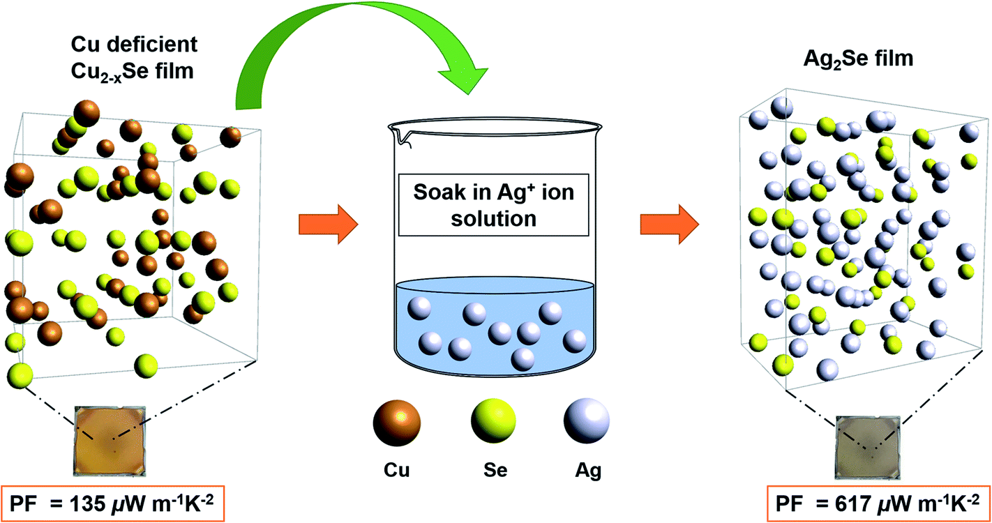 | ||
| Fig. 1 Schematic describing the process in which a Cu-deficient Cu2−xSe thin film transforms into a Ag2Se thin film by fully immersing the Cu2−xSe thin film into a Ag+-rich solution for different amounts of time followed by annealing. Ag+ concentration gradient is established between the soaking solution and the thin film drives the Ag+ ions to diffuse into the Cu2−xSe crystal lattice and replace the Cu+ ions. Electrically, this process results in a switching of majority carrier type from p-type (Cu2−xSe) to n-type (Ag2Se) and an increase in the average PF from 135 μW m−1 K−2 to 617 μW m−1 K−2. The photographs show the Cu2−xSe film (before soak) and the Ag2Se film (after soak) on glass substrates. | ||
Experimental
Synthesis of Ag2Se thin films from Cu2−xSe template films
Copper(I) selenide (Cu2Se, >99.95%), ethylenediamine (H2NCH2CH2NH2, >99%), ethanedithiol (HSCH2CH2SH, >98+%), silver(I) nitrate (AgNO3, >99.9%), acetonitrile (C2H3N, anhydrous, 99.8%), acetone (C3H6O), isopropyl alcohol (C3H8O, 99%) and methanol (CH3OH) were purchased from Sigma-Aldrich. All the chemicals were used as received without further purification.The following steps were performed in a nitrogen-filled glovebox. 100 mg of Cu2Se was weighed and transferred into a 5 mL glass vial. 2 mL of ethylenediamine (en) was measured and transferred to the glass vial, followed by 0.2 mL of ethanedithiol (edtH2) to the same glass vial. The solution was stirred magnetically at 35 °C for about 20 minutes until the solution turned dark brown.
The glass substrates (9.5 mm × 9.5 mm) were sonicated three times for 5–7 minutes in acetone, isopropyl alcohol and methanol respectively. To fabricate a Cu2−xSe thin film with thickness ranges between 70–100 nm, 35 μL of Cu2Se thiol-amine solution was spun coat on a glass substrate at 1800 rpm for 60 seconds. The coated substrate was left on the hot plate to allow the solvent to dry at 35 °C for 2 minutes. The temperature of the hot plate was ramped up to 350 °C by increasing the temperature by 50 °C every 5 minutes. The thin film was annealed on the hot plate for one hour after the temperature reached 350 °C. After an hour, the hot plate was switched off which allowed the thin film to cool down to room temperature. All Cu2−xSe thin films were prepared using the same procedures mentioned above.
To prepare for the Ag+ ion soaking process, 19 mg of AgNO3 was measured, transferred into the glovebox and dissolved in 10 mL of methanol in a glass vial to form a 0.01 M AgNO3 solution. 10 mL of methanol was prepared in a separate glass vial. Previously fabricated Cu2−xSe thin films were held by a tweezer, soaked into the 0.01 M Ag+ ion solution for varying amounts of time and slowly transferred to the pure methanol solution for 45–60 seconds to wash out the excess Ag+ ions from the surface of the thin film. The Ag2Se thin film was placed on the hot plate at 50 °C to dry out the excess solvent and annealed at 350 °C for 30 minutes to repair any cracks and/or release any trapped ions at the grain boundaries during the CE process. The procedure was repeated for each thin film.
Materials characterizations
To characterize the morphology, structure and composition of the Cu2−xSe template samples and the post-soaked Ag2Se samples, we performed scanning electron microscopy (SEM), X-ray diffraction (XRD), X-ray photoelectron spectroscopy (XPS), inductively coupled plasma mass spectrometry (ICP-MS) and TE measurements on our samples. We also performed electrical measurements via the standard four-probe van-der-Pauw method and Seebeck measurements using small Peltier units (CUI Inc.) to measure the induced TE voltage created by various temperature gradients across the sample. Electrical measurements and Seebeck measurements were run via a LabVIEW program along with Keithley 2400 sourcemeters and Keithley 2000 multimeters. Hall carrier concentrations were also obtained using an Ecopia HMS-5000 variable temperature Hall effect measurement system. Thermal conductivity data was extracted using the differential 3ω method using an SR865A lock-in amplifier from Stanford Research Systems (ESI, Fig. S1 and S2†). Film thickness measurements were analyzed via a Veeco Dektak 150 profilometer. Full details about the characterizations can be found in the ESI† along with ESI figures.In addition, error bars were added to each plot in Fig. 6 to show the precision and reliability of our data. Aside from the instrumental errors, the major error for the electrical conductivity values came from the measurement of thickness (standard deviation = ±10 nm) using the profilometer. The detailed error analysis calculations are shown in the ESI† section.
Results and discussion
In many CE reactions for semiconductors, Cd-based and Cu-based NCs have been used as ubiquitous nanocrystal templates to fabricate complex nanomaterials that are otherwise hard to obtain under standard conditions.48,49,53 To form a thin-film NC template, we adopted a method developed by Webber et al. which demonstrated that bulk copper chalcogenides such as Cu2Se, Cu2Te and Cu2S can be dissolved in a thiol-amine solution mixture and be cast as thin films on substrates.45,51,54,55 However, bulk Ag2Se powder fails to do so at ambient conditions (see ESI, Fig. S3†).45,50 To overcome this issue, we use an innovative combination of thiol-amine dissolution and CE techniques to realize a simple pathway to obtaining high-performance Ag2Se thin films.We rationalize the CE using a mix of thermodynamic and kinetic parameters. The thermodynamic driving force of the CE reaction is determined by a number of factors including crystal lattice energy, dissociation and solvation energies, dislocation energies and interfacial strain energy.49 To predict the likelihood of the transformation from Cu2Se to Ag2Se in bulk at room temperature, we conducted calculations on the dissociation and solvation energies during the CE reaction, as suggested in a report by Rivest et al.49 The overall CE equation is described as,
| 2Ag+ (liquid) + Cu2Se (NCs) → Ag2Se (NCs) + 2Cu+ (liquid) |
The equation describes an isovalent system where Ag+ ions are the incoming cations, Cu is the parent cation and Se is the parent anion in the NCs. The thermodynamics of the system can be described in terms of several elementary steps of the CE reaction using the approximate free energy values obtained from past literature, as shown in the following equations:
| Cu2Se → 2Cu + Se dissociation energy: 255.2 ± 14.6 kJ mol−1 (ref. 56) | (1) |
| Ag+ → Ag desolvation energy: 350 kJ mol−1 (ref. 57) | (2) |
| 2Ag + Se → Ag2Se association energy: −210 ± 14.6 kJ mol−1 (ref. 56) | (3) |
| Cu → Cu+ solvation energy: −400 kJ mol−1 (ref. 57) | (4) |
The net energy of the overall transformation is calculated to be: 255.2 + 350 −210 − 400 = −4.8 kJ mol−1. The negative value suggests that the CE reaction is spontaneous at room temperature, and hence is thermodynamically favorable. However, kinetic factors such as activation energy barriers and ion diffusivity also play an important role in determining the outcome of the reactions and the nature of the final products.24,49 Cation exchanging on the nanoscale reduces the limitations stemming from the bulk solid-state exchange. The larger surface area of NCs reduces the sub-reaction activation energy barriers which exist mostly in bulk solid-state exchange, meaning that CE reactions in NCs could happen almost spontaneously. The high curvature surfaces of NCs and low coordination facets that serve as high-energy sites would also reduce the nucleation reaction barriers in NCs and facilitate nucleation.49 Normally, a large excess of incoming cations creating a concentration gradient will be sufficient to drive the reaction at room temperature. Additionally, both Ag+ and Cu+ have high mobility due to their small ionic radii and are both soluble in common solvents such as acetonitrile.
Scanning electron microscopy (SEM) images presented in Fig. 2 show the quality of the thin film sample before and after the soaking process. No significant change in the morphology between the before-soaked Cu2−xSe and post-soaked Ag2Se polycrystalline thin films is observed with grain sizes on the order of tens of nanometers. While there are a few noticeable voids in the Ag2Se film, overall the films are continuous and give reliable TE measurements as will be discussed later. The grain size and morphology of the initial Cu2−xSe film and resultant Ag2Se film were mainly controlled by the annealing temperature. We annealed our Cu2−xSe samples after dissolution for one hour at 350 °C (which gave us the best quality films) and our Ag2Se samples after soaking at 350 °C for 30 minutes. Once the initial Cu2Se films are fabricated, annealing time does not seem to have a significant impact on grain size or domain size, as shown in the SEM images where there is no drastic change in grain size before and after annealing our Ag2Se sample. The grain size we obtained for Cu2−xSe and Ag2Se is estimated to be between 30–50 nm based on the SEM data.
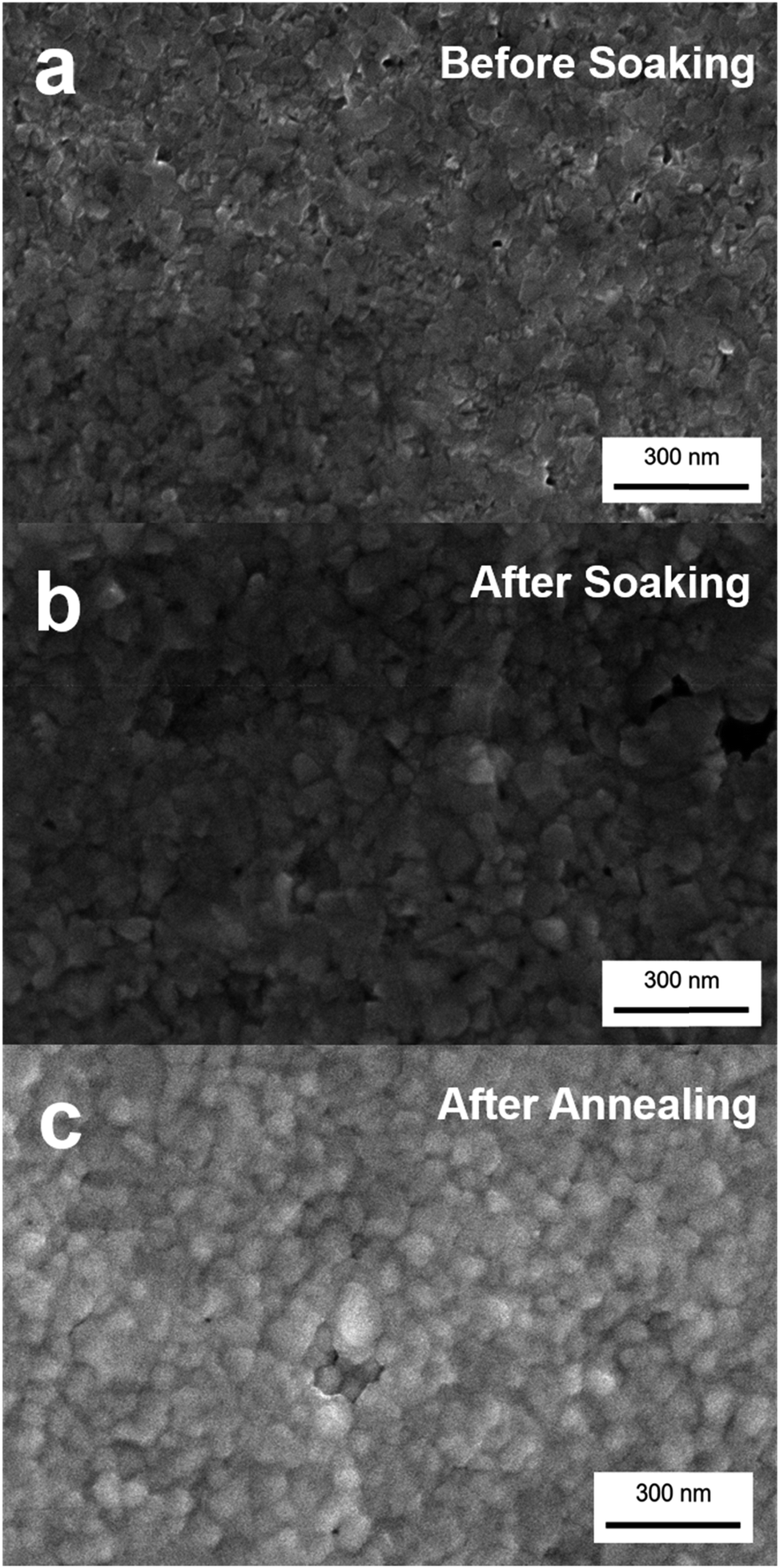 | ||
| Fig. 2 Scanning electron microscope (SEM) images of (a) Cu2−xSe thin film sample before soaking (b) Ag2Se thin film after soaking and (c) the Ag2Se sample post annealing. The images demonstrate the nanocrystalline grain structure as well as the continuous void-free nature of the Cu2−xSe and the Ag2Se films. Annealing does not significantly affect the average grain size of the Ag2Se film. | ||
Energy dispersive X-ray spectroscopy (EDS) presented in Fig. 3 shows the thin film sample before soaking, revealing the presence of Cu and Se while the post-soaked sample indicates the presence of Ag and Se and the absence of Cu, clearly showing that most of the Cu+ ions were substituted during the soaking process for Ag+ ions in the thin film lattice. The rest of the elements such as O, Si, Na, K, Al, Zn originate from the glass substrate and impurities therein. We also detect a minute amount of sulfur from residual thiols in the samples.
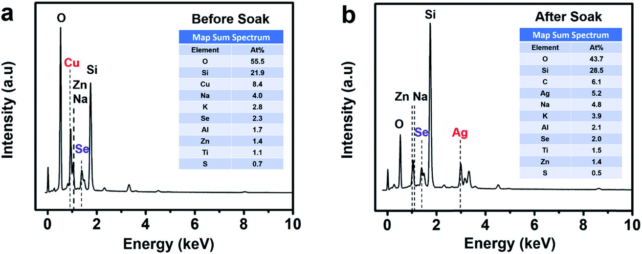 | ||
| Fig. 3 Energy dispersive X-ray spectroscopy (EDS) of (a) a Cu2−xSe sample on glass before soaking and (b) a Ag2Se sample on glass after soaking and annealing. Before soaking, the sample shows peaks corresponding to Cu and Se elements, while after soaking the sample shows only Ag and Se peaks, indicating that the Cu2−xSe sample has converted into Ag2Se. The rest of the elements detected by EDS, including Si and O are from the glass substrate and trace amounts of Na, K, Al, and Zn are from glass impurities as well as a minute amount of sulfur from residual thiols. | ||
To further confirm whether our Cu2−xSe thin film sample was converted into Ag2Se via ion exchange technique, we used X-ray photoelectron spectroscopy (XPS) to identify the presence of Cu and Se before soaking, and the presence of Ag and Se after soaking and annealing. We observe the two Cu peaks disappear as shown in Fig. 4a and the Se peak shifts to the right slightly as shown in Fig. 4c after CE. The Se peak shift may be attributed to the change of Se valence state due to the reduction of Cu vacancies and the occupancy of Ag ions within the lattice.51 The Ag peaks appearing at ∼369 eV and at ∼375 eV illustrate a strong presence of Ag within the thin film sample after soaking as shown in Fig. 4b.
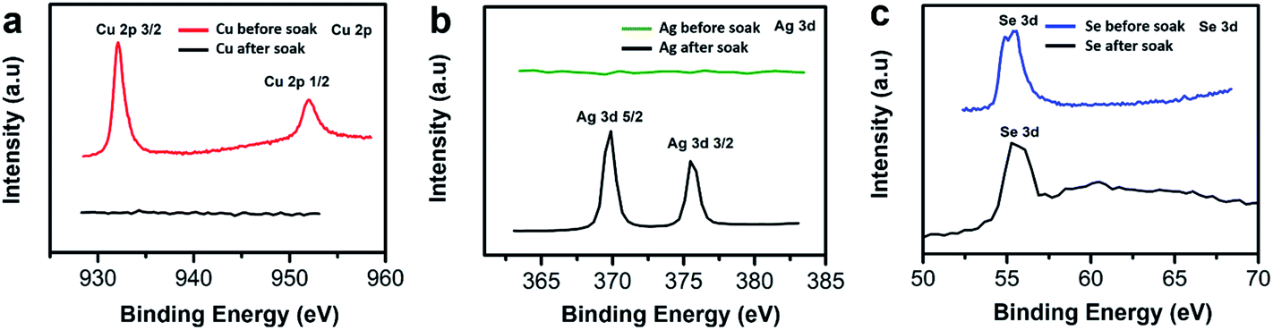 | ||
| Fig. 4 X-ray photoelectron spectroscopy (XPS) images of (a) Cu peaks at 2p orbital in Cu2−xSe sample before (red) and after (black) soaking, (b) Ag peaks at 3d orbital before (green) and after (black) soaking, (c) Se peaks at 3d orbital before (blue) and after (black) soaking. | ||
To validate the structural transformation from Cu2−xSe to Ag2Se within the crystal lattice of our thin film sample, we performed X-ray diffraction (XRD) analysis on our Cu2−xSe samples before and after soaking in a Ag+ salt solution. We compare the XRD data of our Cu2−xSe sample with Cu1.95Se and Cu2Se reference files and the XRD data of our post-soak Ag2Se sample with tetragonal and orthorhombic Ag2Se reference files as shown in Fig. 5. The XRD data for the as-fabricated Cu2−xSe sample closely resembles the Cu1.95Se reference sample.58 Compared to the peaks at 26.3° and 43.6° for the Cu1.95Se reference,58 the major peaks in our Cu2−xSe are shifted slightly by 0.5° and 1.2° respectively, indicating that the unit cell in the Cu2−xSe lattice shrinks when nanostructured. Post-soaked Ag2Se samples are analyzed in a similar fashion as Cu2−xSe. In the post-soaked sample, the Cu2−xSe peaks at 26.9° and 44.8° disappear. The XRD peaks in our post-soaked Ag2Se samples match some of the orthorhombic reference peaks and some of the 10 nm tetragonal Ag2Se XRD peaks based on earlier reports from our group.22 It is postulated that the phase of Ag2Se relies on the crystallite size.61,62 From our data, we observe that our post-soaked Ag2Se thin film sample is a phase mixture of orthorhombic and tetragonal structures with the dominant phase being tetragonal.22 This is expected due to the phase transition between tetragonal and orthorhombic phases occurring at a crystallite size of 40 nm which is around the average size of our grain sizes (∼30–50 nm) as seen in Fig. 2.22,41,42 The post-soaked sample XRD also confirms that, due to the absence of any detectable Cu2Se-related XRD peaks, a complete exchange between Ag+ ions and Cu+ ions occurred during the soaking process.
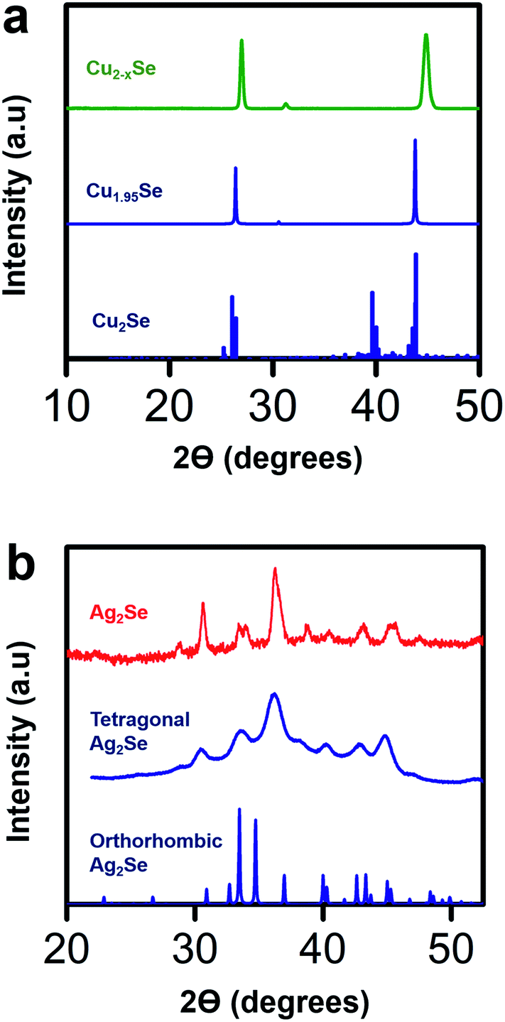 | ||
| Fig. 5 (a) X-ray diffraction (XRD) data for a spin-coated Cu2−xSe sample before soak (green), reference powder diffraction data for a Cu1.95Se sample (blue, ICSD-243957)58 and reference data for a perfectly stoichiometric Cu2Se (blue)59 with a low temperature α-phase. As the XRD data of the Cu2−xSe sample closely resembles that of the Cu1.95Se sample, the Cu deficiency of the Cu2−xSe sample is estimated to be roughly about x = 0.05. (b) XRD data for a Ag2Se film (red) after soaking in Ag+ ion solution for 40 minutes and annealing at 350 °C for 30 minutes, reference data for a tetragonal Ag2Se film (blue)22 and reference data for an orthorhombic Ag2Se film (blue, ICSD-261822).60 The XRD patterns show that the post-soaked annealed Ag2Se film has a mixed phase of tetragonal and orthorhombic structures with a dominant tetragonal phase. | ||
The TE properties of the thin films were measured at room temperature. We tested several different soaking times: 1 min, 5 min, 10 min, 20 min, 40 min and 60 min. Results show that the TE properties remain mostly consistent across different soaking times. The Cu2−xSe thin films with an average thickness of 80 ± 10 nm exhibit an average electrical conductivity of nearly 2.39 ± 0.3 × 10⁵ S m−1 at room temperature. The high electrical conductivity of the Cu2−xSe thin film may be attributed to the high carrier concentration of holes due to Cu-vacancies. Post soaking in Ag-solution, all the samples exhibit a significant drop in electrical conductivity due to the rapid diffusion of Ag+ guest ions into both the vacant sites and interstitial sites leading to early phases of transformation from p-type Cu2Se to n-type Ag2Se. Therefore, short soak times will result in mixed p-type and n-type transport. Rather than exchanging the Cu+ at the surface of the nanocrystalline grains, the Ag+ ions can also diffuse into Cu2−xSe grains and initiate the CE at preferred regions called “reaction zones”.24,52 After a longer soaking time, more “reaction zones” form, more CE reactions take place and Cu+ ions continue to be removed from the lattice. Overall, the electrical conductivities vary little over soaking time showing high consistency.
Immediately after soaking, we observe a sign reversal of the Seebeck coefficient (Fig. 6b) from positive (p-type) to negative (n-type), consistent with our thermodynamic analysis that the CE reaction occurs spontaneously to form n-type Ag2Se from p-type Cu2Se. Seebeck coefficient values stay mostly the same with an average value of −90 ± 6.32 μV K−1 for various soak times. By combining electrical conductivity and Seebeck coefficient values, PF of the films were obtained, as shown in Fig. 6c. The PF values fluctuate slightly within a small range with an average value of 617 ± 82 μW m−1 K−2. While the maximum PF value, 825 μW m−1 K−2, occurs at 5 min soak time we believe that the location and concentration of the residual Cu atoms in the post-soaked sample play a synergistic role in contributing to the higher electrical conductivity compared to all other post-soaked samples (Table 1). Future experiments will be directed to understand the exact role of the Cu-ions. After 60 minutes, the amount of Cu-ions in the sample saturate out at nearly 4% (Table 1). We hypothesize that longer exposure times might lead to back diffusion of Cu+ ions into the Ag2Se lattice thus limiting the CE.
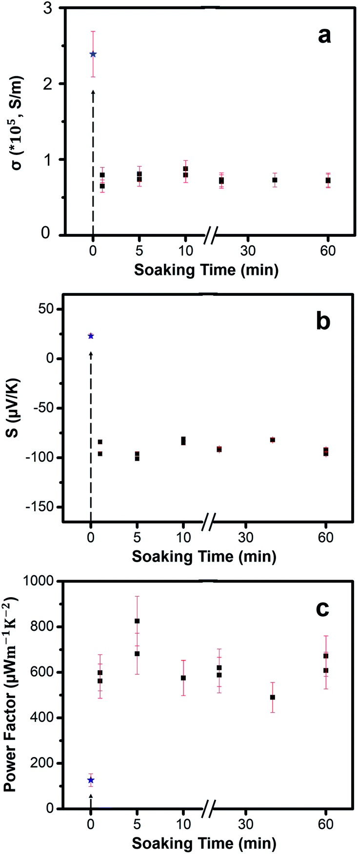 | ||
| Fig. 6 (a) Electrical conductivity of as-fabricated Cu2−xSe sample (blue star) and Ag2Se samples (black squares) as a function of soaking time in Ag+ ion solution. The dotted line at 0 minutes indicates the electrical conductivity of the p-type Cu2−xSe thin film. Our results show that the amount of soaking time does not significantly affect the electrical conductivity. (b) Seebeck coefficient of Cu2−xSe sample and Ag2Se samples as a function of soaking time in Ag+ ion solution. The sign of Seebeck coefficient changes from positive to negative indicating a transformation from p-type Cu2−xSe to n-type Ag2Se. (c) PF data as a function of soaking time. The average PF value measured from 11 samples is 617 ± 82 μW m−1 K−2 and the maximum PF obtained is 825 μW m−1 K−2 after 5 minutes of soaking time. | ||
| Soak time | Mobility [cm2 V−1 s−1] | Carrier density [cm−3] | Ag/Cu molar ratio in Ag2Se sample |
|---|---|---|---|
| 1 min | 2.80 × 10³ | 5.79 × 10¹⁷ | 2.914 |
| 5 min | 3.62 × 10³ | 3.22 × 10¹⁷ | 5.648 |
| 5 min | 2.64 × 10³ | 5.98 × 10¹⁷ | 10.984 |
| 10 min | 1.24 × 10³ | 6.15 × 10¹⁷ | 21.113 |
| 60 min | 3.68 × 10³ | 3.40 × 10¹⁷ | 25.54 |
To observe how the concentration of Cu+ ions vary with soaking time, we performed ICP-MS to obtain a quantitative analysis on how the Cu+ ions are being removed over time. It is difficult to confirm with certainty that there is a complete exchange between Ag+ and Cu+ ions based on our ICP results. As seen in Table 1, the ICP results show that there exists a sizeable amount of Cu+ ions in the post-soaked Ag2Se sample, but with an increase in the soaking time qualitatively the amount of Cu+ ions in the sample decreases monotonically based on the increasing Ag/Cu ratio. The TE performance is not severely affected, however, suggesting that the Cu+ ions may be loosely bound on the surface or trapped in grain boundaries rather than actively doping the material. This is also supported by Hall carrier concentration measurements which show a relatively constant carrier concentration and Hall mobility values across the post-soaked samples. While Hall measurements are not completely accurate for nano-grained polycrystalline samples, qualitatively we observe that all our samples show almost similar values. We suspect that the low carrier density could be attributed to the residual Cu atoms and the sulfur from the thiols as shown in the EDS data in Fig. 3. Further experiments need to be conducted to explore the effect of these residual Cu atoms and sulfur on the TE properties.
Last but not the least, in order to quantify the ZT value for our samples, we conducted room temperature thermal conductivity measurements using the differential 3ω method and obtained a value of 0.53 ± 0.18 W m−1 K−1 (details in ESI†). The total thermal conductivity (κ) typically comprises of a lattice contribution (κl) and an electronic contribution (κe). κe can be approximated as LTσ, where L is the Lorenz number (∼1.8 × 10⁻⁸ V2 K−2), T is the absolute temperature (300 K in our case) and σ is the electrical conductivity (72![[thin space (1/6-em)]](https://www.rsc.org/images/entities/char_2009.gif) 886 S m−1 for the sample measured) which gives us a value of 0.394 W m−1 K−1 and thus a value of 0.136 W m−1 K−1 for κl. Compared to the bulk values of κl = 0.5 W m−1 K−1,21 our sample shows an almost 73% reduction in the lattice thermal conductivity values which is most likely due to the nano-grained structure (average grain sizes between 30–50 nm) of our thin film samples. Consequently, we obtain an average ZT value of around 0.35 with a peak ZT value of 0.46 at a 5 minute soak time. If the residual Cu atoms and sulfur could be removed or their concentration be reduced from our Ag2Se thin films, it would possibly drive up the ZT value to around 1. Compared to the ZT values in bulk powder ranging from 0.32 to 0.99, our average ZT value of 0.35 obtained from a completely solution-processed technique is competitive with bulk values without any need for hot pressing or spark plasma sintering.
886 S m−1 for the sample measured) which gives us a value of 0.394 W m−1 K−1 and thus a value of 0.136 W m−1 K−1 for κl. Compared to the bulk values of κl = 0.5 W m−1 K−1,21 our sample shows an almost 73% reduction in the lattice thermal conductivity values which is most likely due to the nano-grained structure (average grain sizes between 30–50 nm) of our thin film samples. Consequently, we obtain an average ZT value of around 0.35 with a peak ZT value of 0.46 at a 5 minute soak time. If the residual Cu atoms and sulfur could be removed or their concentration be reduced from our Ag2Se thin films, it would possibly drive up the ZT value to around 1. Compared to the ZT values in bulk powder ranging from 0.32 to 0.99, our average ZT value of 0.35 obtained from a completely solution-processed technique is competitive with bulk values without any need for hot pressing or spark plasma sintering.
Conclusions
In conclusion, we report an efficient strategy for fabricating nanostructured Ag2Se thin films via an ion exchange technique between Cu+ ions and Ag+ ions at room temperature. Starting from a low-cost p-type Cu2−xSe template prepared by a thiol-amine dissolution process, n-type Ag2Se thin films were made by simply soaking the Cu2−xSe thin films into a Ag+ ion solution while maintaining mostly the original morphology of Cu2−xSe thin films. The Seebeck coefficient of the thin films post-soaking switches from positive to negative values indicating the change in nature of carrier transport. The thermal conductivity of Ag2Se is measured to be 0.53 W m−1 K−1. The average electrical conductivity of the post-soaked samples is around 7.5 × 10⁴ S m−1. Based on the values of these three parameters, we obtain an average PF of 617 ± 80 μW m−1 K−2 and an average ZT of 0.35 at room temperature with an overall maximum PF of 825 μW m−1 K−2. Furthermore, the soaking approach is a safe, solution-processable, economical fabrication technique which could be potentially useful in industrial scale-up production. Our results demonstrate that Ag2Se thin film materials can become one of the most promising n-type materials for use in a variety of TE applications at a large scale.Conflicts of interest
The authors declare no conflicts of interest.Acknowledgements
The authors thank the Tandon School of Engineering at New York University for financial support through start-up funds. The authors also gratefully acknowledge support for instrument use, scientific and technical assistance from the NYU Shared Instrumentation Facility through the Materials Research Science and Engineering Center (MRSEC) and MRI Programs of the National Science Foundation under Award Numbers DMR-1420073 and DMR-0923251. The X-ray microdiffractometer with GADDS was acquired through the support of the National Science Foundation under Award Number CRIF/CHE-0840277 and the NSF MRSEC Program under Award Number DMR-0820341. The authors would like to acknowledge the Imaging Facility of Advanced Science Research Center at the Graduate Center of CUNY for instrument use, scientific and technical assistance. The authors would also like to acknowledge the Surface Science Facility at Advanced Science Research Center of Graduate Center in CUNY for instrument use, scientific and technical assistance. Finally, M. R. S. and A. S. would also like to thank the National Science Foundation for support under Award ECCS-1809064, and S. B. H. and D. K. K. would like to thank the National Science Foundation for support under Award ECCS-1809112. Z. Y. and F. Y. acknowledge the start-up support from the Stevens Institute of Technology.References
- C. McGlade and P. Ekins, Nature, 2015, 517, 187 CrossRef CAS PubMed.
- U. S. E. I. Administration, Energy use in industry, https://www.eia.gov/energyexplained/use-of-energy/industry.php, accessed 09/17, 2019.
- S. Brückner, S. Liu, L. Miró, M. Radspieler, L. F. Cabeza and E. Lävemann, Appl. Energy, 2015, 151, 157–167 CrossRef.
- A. Allouhi, Y. El Fouih, T. Kousksou, A. Jamil, Y. Zeraouli and Y. Mourad, J. Cleaner Prod., 2015, 109, 118–130 CrossRef.
- D. M. Rowe, Thermoelectrics Handbook: Macro to Nano, CRC/Taylor & Francis, 2005 Search PubMed.
- Y. Ding, Y. Qiu, K. Cai, Q. Yao, S. Chen, L. Chen and J. He, Nat. Commun., 2019, 10, 841 CrossRef PubMed.
- Y. Du, K. Cai, S. Chen, H. Wang, S. Z. Shen, R. Donelson and T. Lin, Sci. Rep., 2015, 5, 6411 CrossRef CAS PubMed.
- L. M. Goncalves, J. G. Rocha, C. Couto, P. Alpuim, G. Min, D. M. Rowe and J. H. Correia, J. Micromech. Microeng., 2007, 17, S168–S173 CrossRef CAS.
- M. Martín-González, O. Caballero-Calero and P. Díaz-Chao, Renewable Sustainable Energy Rev., 2013, 24, 288–305 CrossRef.
- J. R. Sootsman, D. Y. Chung and M. G. Kanatzidis, Angew. Chem., Int. Ed. Engl., 2009, 48, 8616–8639 CrossRef CAS PubMed.
- S. V. Faleev and F. Léonard, Phys. Rev. B: Condens. Matter Mater. Phys., 2008, 77, 214304 CrossRef.
- K. Kishimoto, K. Yamamoto and T. Koyanagi, Jpn. J. Appl. Phys., 2003, 42, 501–508 CrossRef CAS.
- C. Gayner and Y. Amouyal, Adv. Funct. Mater., 2019, 1901789 CrossRef.
- D.-K. Ko, Y. Kang and C. B. Murray, Nano Lett., 2011, 11, 2841–2844 CrossRef CAS PubMed.
- J. R. Durán Retamal, C.-F. Kang, D.-H. Lien, W.-C. Kuo, Z.-Y. Juang, M.-L. Tsai, C.-H. Ho, J.-Y. Juang, V. K. S. Hsiao, Y.-H. Chu, L.-J. Li, Y. Wu and J.-H. He, Adv. Mater., 2018, 30, 1705385 CrossRef PubMed.
- B. Chen, M. Kruse, B. Xu, R. Tutika, W. Zheng, M. D. Bartlett, Y. Wu and J. C. Claussen, Nanoscale, 2019, 11, 5222–5230 RSC.
- N. A. Rongione, M. Li, H. Wu, H. D. Nguyen, J. S. Kang, B. Ouyang, H. Xia and Y. Hu, Adv. Electron. Mater., 2019, 5, 1800774 CrossRef.
- S. W. Finefrock, H. Yang, H. Fang and Y. Wu, Annu. Rev. Chem. Biomol. Eng., 2015, 6, 247–266 CrossRef CAS PubMed.
- B. Xu, J. Zhang, G. Yu, S. Ma, Y. Wang and Y. Wang, J. Appl. Phys., 2018, 124, 165104 CrossRef.
- K. H. Lim, K. W. Wong, Y. Liu, Y. Zhang, D. Cadavid, A. Cabot and K. M. Ng, J. Mater. Chem. C, 2019, 7, 2646–2652 RSC.
- T. Day, F. Drymiotis, T. Zhang, D. Rhodes, X. Shi, L. Chen and G. J. Snyder, J. Mater. Chem. C, 2013, 1, 7568–7573 RSC.
- A. Sahu, D. Braga, O. Waser, M. S. Kang, D. Deng and D. J. Norris, Nano Lett., 2014, 14, 115–121 CrossRef CAS PubMed.
- M. Ferhat and J. Nagao, J. Appl. Phys., 2000, 88, 813–816 CrossRef CAS.
- L. De Trizio and L. Manna, Chem. Rev., 2016, 116, 10852–10887 CrossRef CAS PubMed.
- S. Maiti, S. Maiti, A. H. Khan, A. Wolf, D. Dorfs, I. Moreels, F. Schreiber and M. Scheele, Chem. Mater., 2019, 31, 2443–2449 CrossRef CAS.
- E. Dilena, D. Dorfs, C. George, K. Miszta, M. Povia, A. Genovese, A. Casu, M. Prato and L. Manna, J. Mater. Chem., 2012, 22, 13023–13031 RSC.
- P. Junod, H. Hediger, B. Kilchör and J. Wullschleger, Philos. Mag., 1977, 36, 941–958 CrossRef CAS.
- P. Boolchand and W. J. Bresser, Nature, 2001, 410, 1070–1073 CrossRef CAS PubMed.
- F. F. Aliev, M. B. Jafarov and V. I. Eminova, Semiconductors, 2009, 43, 977–979 CrossRef CAS.
- C. Xiao, J. Xu, K. Li, J. Feng, J. Yang and Y. Xie, J. Am. Chem. Soc., 2012, 134, 4287–4293 CrossRef CAS PubMed.
- W. Mi, P. Qiu, T. Zhang, Y. Lv, X. Shi and L. Chen, Appl. Phys. Lett., 2014, 104, 133903 CrossRef.
- E. J. T. Frederick Lutgens, Essentials of geology, Prentice Hall, Upper Saddle River, NJ, 7th edn, 2000 Search PubMed.
- G. Henshaw, I. P. Parkin and G. A. Shaw, J. Chem. Soc., Dalton Trans., 1997, 231–236, 10.1039/a605665b.
- G. Sáfrán, O. Geszti, G. Radnóczi and P. B. Barna, Thin Solid Films, 1998, 317, 72–76 CrossRef.
- R. Dargel, M. Azeroual, B. Mogwitz, J. Janek and C. Vogt, J. Mater. Sci., 2007, 42, 7375–7380 CrossRef CAS.
- W. Wang, Y. Geng, Y. Qian, M. Ji and Y. Xie, Mater. Res. Bull., 1999, 34, 877–882 CrossRef CAS.
- J. A. Perez-Taborda, O. Caballero-Calero, L. Vera-Londono, F. Briones and M. Martin-Gonzalez, Adv. Energy Mater., 2018, 8, 1702024 CrossRef.
- J. A. Perez-Taborda, L. Vera, O. Caballero-Calero, E. O. Lopez, J. J. Romero, D. G. Stroppa, F. Briones and M. Martin-Gonzalez, Adv. Mater. Technol., 2017, 2, 1700012 CrossRef.
- D. Wang, T. Xie, Q. Peng and Y. Li, J. Am. Chem. Soc., 2008, 130, 4016–4022 CrossRef CAS PubMed.
- J. Pei, G. Chen, D. Jia, R. Jin, H. Xu and D. Chen, New J. Chem., 2013, 37, 323–328 RSC.
- A. Sahu, L. Qi, M. S. Kang, D. Deng and D. J. Norris, J. Am. Chem. Soc., 2011, 133, 6509–6512 CrossRef CAS PubMed.
- A. Sahu, A. Khare, D. D. Deng and D. J. Norris, Chem. Commun., 2012, 48, 5458–5460 RSC.
- S. B. Hafiz, M. R. Scimeca, P. Zhao, I. J. Paredes, A. Sahu and D.-K. Ko, ACS Appl. Nano Mater., 2019, 2, 1631–1636 CrossRef CAS.
- D. H. Webber, J. J. Buckley, P. D. Antunez and R. L. Brutchey, Chem. Sci., 2014, 5, 2498–2502 RSC.
- C. L. McCarthy, D. H. Webber, E. C. Schueller and R. L. Brutchey, Angew. Chem., Int. Ed., 2015, 54, 8378–8381 CrossRef CAS PubMed.
- I. G. Dance, Polyhedron, 1986, 5, 1037–1104 CrossRef CAS.
- D. H. Son, S. M. Hughes, Y. Yin and A. Paul Alivisatos, Science, 2004, 306, 1009–1012 CrossRef CAS PubMed.
- N. A. Moroz, A. Olvera, G. M. Willis and P. F. P. Poudeu, Nanoscale, 2015, 7, 9452–9456 RSC.
- J. B. Rivest and P. K. Jain, Chem. Soc. Rev., 2013, 42, 89–96 RSC.
- Z. Lin, C. Hollar, J. S. Kang, A. Yin, Y. Wang, H.-Y. Shiu, Y. Huang, Y. Hu, Y. Zhang and X. Duan, Adv. Mater., 2017, 29, 1606662 CrossRef PubMed.
- M. R. Scimeca, F. Yang, E. Zaia, N. Chen, P. Zhao, M. P. Gordon, J. D. Forster, Y.-S. Liu, J. Guo, J. J. Urban and A. Sahu, ACS Appl. Energy Mater., 2019, 2, 1517–1525 CrossRef CAS.
- V. Lesnyak, C. George, A. Genovese, M. Prato, A. Casu, S. Ayyappan, A. Scarpellini and L. Manna, ACS Nano, 2014, 8, 8407–8418 CrossRef CAS PubMed.
- F. S. Stinner, Y. Lai, D. B. Straus, B. T. Diroll, D. K. Kim, C. B. Murray and C. R. Kagan, Nano Lett., 2015, 15, 7155–7160 CrossRef CAS PubMed.
- Y. Ma, P. B. Vartak, P. Nagaraj and R. Y. Wang, RSC Adv., 2016, 6, 99905–99913 RSC.
- Z. Lin, Q. He, A. Yin, Y. Xu, C. Wang, M. Ding, H.-C. Cheng, B. Papandrea, Y. Huang and X. Duan, ACS Nano, 2015, 9, 4398–4405 CrossRef CAS PubMed.
- J. N. Plendl and E. P. J. Gl, Z. für Kristallogr. - Cryst. Mater., 1963, 118, 404 CrossRef CAS.
- Y. Marcus, J. Chem. Soc., Faraday Trans., 1991, 87, 2995–2999 RSC.
- E. Eikeland, A. B. Blichfeld, K. A. Borup, K. Zhao, J. Overgaard, X. Shi, L. Chen and B. B. Iversen, IUCrJ, 2017, 4, 476–485 CrossRef CAS PubMed.
- L. Gulay, M. Daszkiewicz, O. Strok and A. Pietraszko, Chem. Met. Alloys, 2011, 4, 200–205 Search PubMed.
- J. Yu and H. Yun, Acta Crystallogr., Sect. E: Struct. Rep. Online, 2011, 67, i45 CrossRef CAS PubMed.
- J. R. Günter and P. Keusch, Ultramicroscopy, 1993, 49, 293–307 CrossRef.
- B. Gates, B. Mayers, Y. Wu, Y. Sun, B. Cattle, P. Yang and Y. Xia, Adv. Funct. Mater., 2002, 12, 679–686 CrossRef CAS.
Footnote |
| † Electronic supplementary information (ESI) available. See DOI: 10.1039/c9na00605b |
| This journal is © The Royal Society of Chemistry 2020 |