
 Open Access Article
 This Open Access Article is licensed under a Creative Commons Attribution-Non Commercial 3.0 Unported Licence
The occupied electronic structure of ultrathin boron doped diamond†
A. C.
Pakpour-Tabrizi
a,
A. K.
Schenk
b,
A. J. U.
Holt
c,
S. K.
Mahatha
c,
F.
Arnold
c,
M.
Bianchi
c,
R. B.
Jackman
a,
J. E.
Butler
d,
A.
Vikharev
e,
J. A.
Miwa
c,
P.
Hofmann
c,
S. P.
Cooil
bf,
J. W.
Wells
 *b and
F.
Mazzola‡
b
*b and
F.
Mazzola‡
b
aLondon Centre for Nanotechnology, Department of Electronic and Electrical Engineering, University College London, 17-19 Gordon Street, London WC1H 0AH, UK
bCenter for Quantum Spintronics, Department of Physics, Norwegian University of Science and Technology, NO-7491 Trondheim, Norway. E-mail: justin.wells@ntnu.no
cDepartment of Physics and Astronomy, Interdisciplinary Nanoscience Center, Aarhus University, 8000 Aarhus C, Denmark
dCubic Carbon Ceramics, 855 Carson Road, Huntingtown, MD 20639, USA
eInstitute of Applied Physics, Russian Academy of Sciences, 46 Ul'yanov Street, Nizhny Novgorod, 603950, Russia
fDepartment of Physics, Aberystwyth University, Aberystwyth SY23 3BZ, UK
First published on 24th February 2020
Abstract
Using angle-resolved photoelectron spectroscopy, we compare the electronic band structure of an ultrathin (1.8 nm) δ-layer of boron-doped diamond with a bulk-like boron doped diamond film (3 μm). Surprisingly, the measurements indicate that except for a small change in the effective mass, there is no significant difference between the electronic structure of these samples, irrespective of their physical dimensionality, except for a small modification of the effective mass. While this suggests that, at the current time, it is not possible to fabricate boron-doped diamond structures with quantum properties, it also means that nanoscale boron doped diamond structures can be fabricated which retain the classical electronic properties of bulk-doped diamond, without a need to consider the influence of quantum confinement.
Diamond is an electrical insulator with spectacular physical properties: it is one of the hardest natural materials,1 has one of the highest thermal conductivities of any elemental material,1,2 a high breakdown field, biocompatibility3 and, contrary to traditional semiconductors, is robust against radiation damage.4 Diamond may be doped with boron either naturally, or during Chemical Vapour Deposition (CVD) film growth5 or with post-growth ion implantation,6 turning diamond semiconducting,7,8 metallic or allowing a superconducting transition under the right conditions,9–11 depending on the dopant concentration. These properties make diamond an appealing candidate for a broad range of applications.12–14 Growing ultrathin (nanometer scale) diamond films may allow minituarised devices to benefit from the exemplary properties of diamond, as well as reducing processing costs for applications where only a thin film is required. In recent years, the ability to grow ultrathin, heavily boron doped diamond layers has been demonstrated15–17 – such doped profiles are typically referred to as δ-doping (or δ-layers) and may have strongly modified electronic properties when compared to thicker films.18–22
δ-Doping consists of engineering a narrow profile (typically from one atomic layer to several nanometers) of electron donor or acceptor species within a host material, either submerged in the bulk (encapsulated, or so-called “capped” δ-layers) or at the surface (unencapsulated, “uncapped” δ-layers),23–25 such that the layer thickness is narrow relative to the ground state wavefunction of the free carrier gas.26 These structures have electronic properties dictated by the interplay of quantum confinement effects, spin27 and charge ordering and the overlap between the host material and the dopants' atomic-wavefunctions.23,25 As an example, phosphorus doped δ-layers in silicon (referred to as Si:P δ-layers) create new low-dimensional electronic states18–20 which influence electrical transport properties.22 The self-consistent Poisson–Schrödinger calculations28,29 indicate that boron-doped δ-layers in diamond, with experimentally achievable thicknesses and dopant densities, will generate a potential which is sufficiently strong and narrow to create quantum confined states; however these states, or any other alterations to the electronic structure as a result of quantum confinement, are yet to be experimentally confirmed.
In this study, we use angle-resolved photoelectron spectroscopy (ARPES) to compare the electronic structure of a 1.8 nm boron doped δ-layer with that of a thick 3 μm boron-doped diamond film, to explore if the electronic structure is modified by nanoscale confinement. ARPES has been demonstrated as an exemplary tool for characterising the occupied electronic structure of low-dimensional systems, providing a clear and unique means of distinguishing electronic states associated with reduced dimensionality from three-dimensional electronic structure,30,31 and has been successfully applied to numerous investigations of Si:P δ-layers,18–21 where new states are formed due to the quantum confinement. Contrary to expectation, our results indicate that the electronic structure of currently achievable δ-doped diamond films is very similar to that of bulk doped diamond. This finding offers some explanation for the observed lack of quantum confinement enhancement in the transport measurements performed by Chicot et al.28,32 and we discuss possible sources of the consistent discrepancy between theoretical expectation and experimental observation.
Experimental details
This study uses a boron-doped δ-layer sample with a nominal thickness of 1.8 nm, and a thick (thickness ∼ 3 μm) boron-doped film. The boron doped δ-layer was grown on a 3.6 mm × 3.6 mm (100) oriented high pressure high temperature (HPHT) Ib substrate, with an intrinsic buffer layer (nominal thickness 0.5 μm) grown using CVD between the δ-layer and substrate. As a comparison, a boron doped thick film was also grown with CVD. The boron doping density, determined with Secondary-Ion Mass Spectrometry (SIMS) is similar in all samples (∼5 × 1020 cm−3). For details, see ref. 15, 33 and 34.The in situ sample preparation consisted of annealing to 350 °C for 8 hours to remove atmospheric contamination, followed by multiple 5 second flashes to 800 °C. All data has been acquired at room temperature, with the k‖ axis aligned along the X–Γ–X direction, determined from the symmetry of constant energy maps acquired during sample alignment. The k⊥ axis is likewise along X–Γ–X. A free-electron final state model31 with an inner potential of 22 eV (ref. 35) has been used for converting units of photon energy into k⊥.36 The photon energy range used in this work is relatively high compared to the typical photon energies used for ARPES. This is necessary as a result of diamond displaying non free-electron final state behaviour in measurements performed at low photon energies;37 a discussion of this, with ESI,† is presented in ref. 34.
Relative energy alignment between measurements has been performed by acquiring the Fermi edge of a gold foil in electrical contact with the sample and aligning this to a common origin for all photon energies in this study. An absolute energy calibration has been performed at hν = 520 eV by integrating the photoemission background (away from any strong features) and identifying the Fermi level. This atypical second step is necessary to compensate for the possibility of a Schottky barrier between the sample and calibration foil,38 as well as the possibility of a photovoltage generated by synchrotron light exposure,39,40 both of which will manifest as an offset in the energy scale of the dataset.
Computational methods
Tight Binding (TB) calculations and Density Functional Theory (DFT) are powerful computational methods for studying the bandstructure of solid state materials (for example, ref. 41 and 42), and should be able to reproduce the pertinent experimental observations and strengthen the understanding of diamond in general and boron δ-doped diamond specifically. DFT calculations for bulk boron doped diamond are readily available, and they satisfactorily reproduce ARPES data collected at higher photon energies (see for example ref. 10). Performing DFT calculations for δ-layer structures is much more challenging: in order to satisfactorily describe the in-plane (lack of) order, and to include a sufficient thickness of undoped host material, a supercell of at least ≈4 × 4 × 100 = 1600 atoms is required,43,44 and this is currently beyond the computational resources available to us (but will hopefully be the topic of future work).TB calculations are generally less computationally demanding and have been performed using the approach of Chadi and Cohen,45 with the TB parameters optimised to fit the data acquired at 410 eV (i.e. Fig. S1(b)†), corresponding to bulk Γ003.46 When comparing TB calculations and data acquired at other photon energies, we have used the same TB parameters but varied the k⊥ value of the calculation in order to correspond with the k⊥ value experimental data. In this work, TB calculations are overlaid on the experimental data and discussed further in the ESI.†34
Results and discussion
Published calculations28,29 show the formation of a confining potential approximately 0.25 eV deep (for a 0.36 nm thick δ-layer, and increasing with layer thickness), inducing confined hole states both above and below the Fermi level, with the typical characteristics expected of such quantum wells – the energy separation between states decreases for thicker δ-layers, and decreases the closer the state is to the top of the well. These simulations assume an atomically sharp δ-layer, with an immediate transition between the heavily doped δ-layer and the surrounding diamond. In practice, boron δ-layers in diamond are grown by adding a boron precursor to the diamond CVD growth process; such a growth process can yield a very sharp junction,17,47 but not as abrupt as in the calculations. In order to address this possible inconsistency, we have carried out SIMS measurements (Fig. 1) on both the diamond sample used here and a Si:P δ-layer with a similar nominal thickness, used in previous work,48 and where pulsed laser atom probe tomography (PLAPT) was also used to confirm the sharpness of the profile. In both cases, the peak doping density, sharpness and width are extremely similar. However, it is also worth pointing out that the SIMS data presented is resolution limited, and hence it is possible that the profile is significantly sharper than Fig. 1 appears to indicate. In any case, based on our previous work on Si:P δ-layers,18–21 we expect such a dopant profile in diamond to give rise to strongly confined 2-dimensional quantum-well states.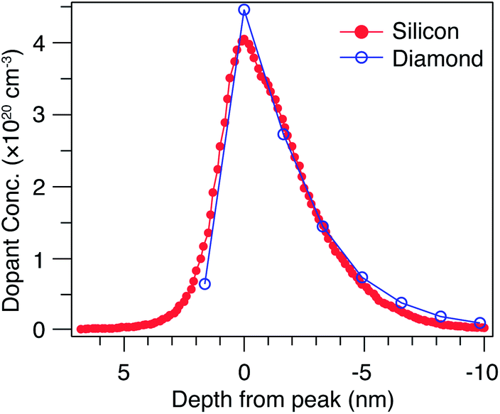 | ||
| Fig. 1 SIMS depth profile of a δ doped silicon and diamond sample. The measured dopant concentration in a boron-doped diamond δ-layer with nominal thickness 1.8 nm is compared with a phosphorus-doped silicon δ-layer of nominal thickness 2 nm. | ||
For a system possessing states as a result of quantum confinement in the direction perpendicular to the surface, one expects to observe features which do not disperse with k⊥. Therefore, slices of constant k‖ slices have been extracted from the ARPES dataset acquired on the δ-layer sample, and are presented in Fig. 2. Within this representation of the data, confined states will be present as non-dispersing features (i.e. horizontal lines across the panels in Fig. 2), with a varying intensity due to the changing photoemission transition matrix elements.49,50Fig. 2 shows no such horizontal features at any value of k‖, suggesting that there are no occupied states uniquely associated with reduced electronic dimensionality within the δ-layer.
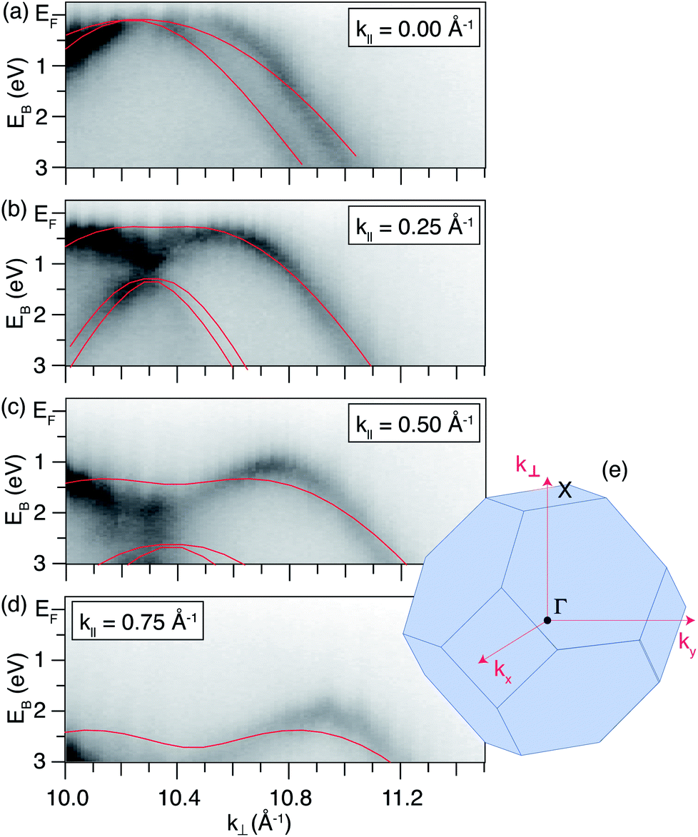 | ||
| Fig. 2 Selected band dispersions with respect to k⊥. (a–d) Constant k‖ slices through the photon energy-dependent dataset (380–460 eV) acquired on the δ-layer sample; the photon energy axis has been converted to k⊥ using the assumption for a free-electron-like final state (k⊥ ≈ 10.0–11.4 Å−1), and the values of k‖ chosen are shown in the panels. Tight-binding calculations are overlaid (red solid lines). (e) Schematic of the bulk Brillouin zone showing the definitions of the axes used. | ||
Dispersions in E(k‖) acquired with selected photon energies on both the δ-layer and bulk film sample are presented in Fig. 3. While we cannot with complete certainty say that the dispersions are identical, the differences between the datasets are minor, and can be attributed to slight variations in doping concentration, sample alignment and impurities. Thus, in addition to not observing quantum well states in the δ-layer, the thickness of the dopant layer does not appear to appear to alter the diamond occupied electronic structure significantly. On the other hand, measurements performed at lower photon energy (Fig. 4), and therefore with increased surface sensitivity, do appear to show a small change in the effective mass of the parabolic band maxima of the δ-layer sample (compared to the thick film). This is accentuated in Fig. 4(c) in which the dispersions for both samples are plotted together. The effective mass of the band plays a role in defining the phase space available for phonon-scattering and hence the magnitude of the electron-phonon coupling strength and therefore the critical temperature for superconductivity.51–53
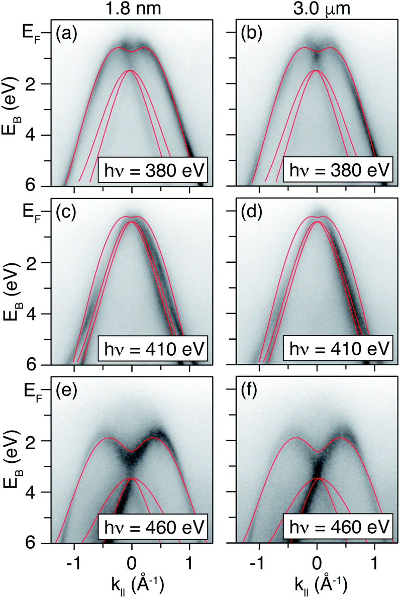 | ||
| Fig. 3 Selected ARPES measurements performed on a 1.8 nm diamond δ-layer sample and the 3.0 μm bulk sample. Measurements performed at: (a and b), a photon energy of 380 eV (≈k⊥ = 10.0), (c and d), a photon energy of 410 eV (≈k⊥ = 10.3, corresponding to the bulk BZ center) and (e and f), a photon energy of 460 eV (≈k⊥ = 11.5). Tight-binding calculations are overlaid (red solid lines). | ||
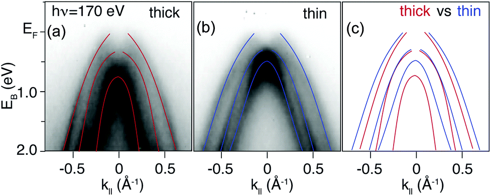 | ||
| Fig. 4 Comparison of the band dispersions from a thin δ-layer sample and a thick sample. Measurements carried out at a photon energy of 170 eV (corresponding to a slice through the bulk BZ center). (a) The 3.0 μm bulk-like sample and (b) the 1.8 nm δ-layer. Both figures are overlaid with parabolic schematic bands, as a “guide-to-the-eye”. (c) Comparison of the two sets of parabolic bands showing that there is a small, but significant, difference in the effective mass for the two samples. | ||
The observed modification of the effective mass can be attributed to electron correlations. Electron–electron correlations have been demonstrated to induce a bandwidth narrowing and to increase the effective mass of the charge carriers when the dimensionality of the sample is reduced.54–56 This picture finds full agreement with our data where both a bandwidth narrowing and an increase of the hole effective mass is observed. In addition, electron–electron interactions are expected to be significant in stabilizing the electronic structure of superconductors and of materials which exhibit a metal–insulator transition, and both of these effects have been documented for boron-doped diamond.9,10,57,58 In these terms, boron δ-doped diamond would constitute a perfect playground for exploring the role of correlation effects and putative superconductivity.59 In any case, the fact that a modification of the effective mass can be seen adds assurance that a dense and narrow dopant profile is indeed present on the lengthscale probed by our ARPES measurements.
Calculations indicate that, for a 1.8 nm boron doped δ-layer in diamond, there will be occupied quantum well states located below the Fermi level28,29 and, thus, presumably observable in ARPES. The lack of such states in our data suggests that either our sample differs from the calculated systems, or that the calculations are an incomplete description of the physical system.
On possible discrepancy between our measurements and the calculations is the layer thickness. Our δ-layer sample is grown so as to produce a dopant profile of 1.8 nm, however, the measured profile by SIMS is limited by the resolution of the instrument. It is therefore possible that the actual dopant profile is sharper, or slightly broader, then the nominal thickness. As shown by Chicot et al. reducing the thickness of the δ-layer leads to a shallower and narrower potential and may create a situation where there are no longer occupied quantum well states (see ref. 28 and 34 for details). On the other hand, from the same calculations, a slightly broader profile is expected to still produce occupied confined states.
Another possible cause for discrepancy is the asymmetry of the confinement potential. In the work of Chicot et al. and Fiori et al. the δ-layer is either sandwiched between two 500 nm slabs of diamond (the “infinite” case), or sandwiched between a 500 nm diamond slab and a 25 nm diamond layer with a Schottky contact (the “semi-infinite” case). In our experiments, the δ-layer is not encapsulated, and hence the potential gradient on the diamond/vacuum interface will be dissimilar (steeper) relative to the bulk side (see ref. 34 for details). This modification to the confinement potential is small, but in principle may cause the occupied states to shift further below the Fermi level (relative to a symmetric well). On the other hand, this is not expected to hinder detection by ARPES, and has not hindered comparable studies on unencapsulated Si:P δ-layers.60
It is also necessary to be aware that atmospheric adsorbates can play a significant role in dramatically increasing the surface doping of both boron-doped and intrinsic diamond (see for example ref. 12 and 61), leading to the creation of a surface 2-dimensional hole gas with unusual properties.62 In our work, the samples are annealed in a pristine UHV environment, and hence we believe that such atmospheric adsorbates are not present. However, the presence/absence of water and other atmospheric species may account for some of the differences in the δ-layer literature – especially for transport measurements performed in air.
It is also conceivable that the available calculations may not accurately describe the physical system. The calculations of Fiori et al. and Chicot et al. assumed that the relative dielectric constant within the δ-layer is 5.7, i.e. that of undoped diamond. While the literature does not cover the specific case of doped diamond, it is known that the dielectric constant of highly doped semiconductors varies with dopant density.60,63 The calculations of Fiori et al. and Chicot et al. also give no details of the screening potential used as part of the calculations. Correctly accounting for the dielectric constant and screening potential will naturally influence the calculations of the potential and charge distribution, and thus the predicted energies of the resulting confined states. Furthermore, Chicot et al. and Fiori et al. use isotropic effective masses (mlh = 0.303m0, mhh = 0.588m0, for the light-hole and heavy-hole states, respectively) taken from the work of Willatzen et al. in their calculations.64 There is little agreement in the literature on hole effective masses in bulk diamond (see Table 1), and in highly doped δ-layers the effective mass anyway appears to be modified. As energy eigenvalues calculated with the Schrödinger equation are dependent on effective mass, it is straightforward to see that this choice will directly effect the theoretical description of the δ-layer electronic structure. Furthermore, Fiori et al. and Chicot et al. do not address the positioning of the dopant atoms, in particular whether they have an ordered or disordered arrangement within the δ-layer. In the case of Si:P δ layers, ordering of the dopants influences the calculated electronic structure in the δ-layer.19,65 Due partly to the computational resources needed, such a study has not been published for boron-doped δ-layers in diamond, but it is reasonable to infer that dopant order, or lack thereof, may also influence the δ-layer electronic structure. In short, there are several differences in the representation of the δ-layer in the calculations compared to the real sample, but none which are obviously responsible for the lack of quantised states in the occupied bandstructure.
It is interesting to notice that the electrical transport measurements of Chicot et al. also found no quantum enhancement of the hole mobility in encapsulated diamond δ-layers,28,32 suggesting that there was no quantum confinement in this case either. Whilst it is possible that our ARPES investigation has somehow failed to observe quantised states, the implications from transport studies seem to support the notion that such states are simply not present.
It is possible that the δ-layer samples grown with the CVD processing methods used here15–17 are not able to produce a sufficiently sharp and narrow dopant profile, or that the lack of quantisation has another cause. On the other hand, a new generation of δ-doped samples (with even sharper doping profiles) will become available.68,69 In any case, further work from both a theoretical and experimental standpoint will be necessary to determine whether diamond δ-layer samples can be fabricated in which quantised confined states are observable.
Finally, we consider the impact these findings have for the application of nanostructured boron-doped diamond grown using current CVD processing methods. The growth of high quality diamond layers typically proceeds at rates on the order of micrometers per hour,5 with the diamond growth rate and defect density typically being inversely related. Thick, high-quality diamond films are therefore associated with long processing times and high cost. While defect density is not necessarily a concern for all applications of doped diamond structures, properties such as electrical and thermal conductivity are hampered by high defect densities.70 Our findings indicate that in the case of boron doped diamond, bulk-like electronic properties can be achieved in exceptionally thin films; which may be seen as an advantage when cost-effective high-quality fabrication is desired. Whilst quantum effects certainly have their uses in quantum electronics,71–73 the era of continued downscaling of traditional silicon-based devices is reaching its limit. The persistence of bulk-like diamond electronic properties at the single nanometer scale suggests that such limitations of downscaling are of less concern for diamond-based electrical components (such as piezoresistive diamond sensors74), thus expanding the potential applications for nanoscale diamond components.
Conclusion
This work uses ARPES to compare the occupied electronic structure of boron δ-doped diamond with bulk boron doped diamond, in order to determine if δ-doped diamond grown with current CVD processing techniques produces a potential sufficiently strong and narrow to give rise to quantum confinement, as suggested by the Poisson–Schrödinger calculations of Chicot et al. and Fiori et al. We instead observed that the occupied electronic structure of the boron δ-doped layer was similar to that of a bulk-like boron doped film, with no additional features to attribute to electron-occupied quantum well states and no modification of the pre-existing bands except for a small modification of the effective mass. While this is contrary to the calculations, the electrical transport measurements performed by Chicot et al.28,32 also showed no quantum confinement related enhancement of the hole mobility in δ-doped diamond. Also suggesting that there may be no quantum confinement. On the other hand, Butler et al.15 using the same samples do see an enhancement of the hole mobility implying that further studies will be necessary to understand the physical cause behind this. Based on our results, it can be expected that regardless, of the size of boron doped diamond components, the desirable electronic properties of bulk boron doped diamond will be retained without being influenced by quantum confinement, an advantageous property for developing miniaturised electrical components.Author contributions
ACPT, RBJ, JWW and FM conceived and instigated the project. JEB and AV produced the samples, and carried out background studies with collaboration with RBJ and ACPT. ACPT, AKS, AJUH, SKM, FA, MB, SPC, JWW and FM carried out the ARPES measurements and data analysis. ACPT, AKS, PH, JWW and FM prepared the final manuscript with input from all authors.Conflicts of interest
There are no conflicts to declare.Acknowledgements
ACPT and AKS contributed equally to this work. RBJ acknowledges the UK's Engineering and Physical Sciences Research Council (EPSRC) for partial funding for this activity (EP/H020055/1) as well as The EC's Horizon 2020 Programme for support from the “GREENDIAMOND” project (ID: 640947). Oliver A. Williams and Souman Mandel (University of Cardiff, UK) are sincerely thanked for the growth of the thick, bulk-like doped diamond film used here. δ-Layer samples were supplied from a collaboration with Diamond Microwave Devices Ltd and Element Six Ltd, whilst the other was produced at the IAP RAS as part of the programme supported by Act 220 of the Russian Government (Agreement no. 14.B25.31.0021). Experimental results were acquired at the ADRESS beamline at SLS, the VUV beamline at Elettra and at beamline I4 of MAX-III. We acknowledge support from Marco Caputo and Vladimir Strocov, Balasubramanian Thiagarajan, and the the other support staff at these facilities. This work was supported by the Research Council of Norway through its Centres of Excellence funding scheme, Project No. 262633, “QuSpin”, and through the Fripro program, Project No. 250985 “FunTopoMat” and 262339 “NEAT”. This work was supported by the Danish Council for Independent Research, Natural Sciences under the Sapere Aude program (Grants No. DFF-4002-00029 and DFF-6108-00409) and by VILLUM FONDEN via the Centre of Excellence for Dirac Materials (Grant No. 11744) and the Aarhus University Research Foundation.References
- J. M. T. Thompson and P. W. May, Philos. Trans. R. Soc., A, 2000, 358, 473 CrossRef.
- R. Berman, F. E. Simon and J. M. Ziman, Philos. Trans. R. Soc., A, 1953, 220, 171 CAS.
- A. Grill, Proceedings of the 4th Specialist Meeting on Amorphous Carbon, Diamond Relat. Mater., 2003, 12, 166 CrossRef CAS.
- C. Bauer, I. Baumann, C. Colledani, J. Conway, P. Delpierre, F. Djama, W. Dulinski, A. Fallou, K. K. Gan, R. S. Gilmore, E. Grigoriev, G. Hallewell, S. Han, T. Hessing, K. Honschied, J. Hrubec, D. Husson, H. Kagan, D. Kania, R. Kass, W. Kinnison, K. T. Knöpfle, M. Krammer, T. J. Llewellyn, P. F. Manfredi, L. S. Pan, H. Pernegger, M. Pernicka, R. Plano, V. Re, S. Roe, A. Rudge, M. Schaeffer, S. Schnetzer, S. Somalwar, V. Speziali, R. Stone, R. J. Tapper, R. Tesarek, W. Trischuk, R. Turchetta, G. B. Thomson, R. Wagner, P. Weilhammer, C. White, H. Ziock and M. Zoeller, Proceedings of the 7th International Wire Chamber Conference, Nucl. Instrum. Methods Phys. Res., Sect. A, 1995, 367, 207 CrossRef CAS.
- B. V. Spitsyn, L. L. Bouilov and B. V. Derjaguin, J. Cryst. Growth, 1981, 52, 219 CrossRef CAS.
- G. Braunstein and R. Kalish, J. Appl. Phys., 1983, 54, 2106 CrossRef CAS.
- A. T. Collins and A. W. S. Williams, J. Phys. C: Solid State Phys., 1971, 4, 1789 CrossRef CAS.
- R. M. Chrenko, Phys. Rev. B: Solid State, 1973, 7, 4560 CrossRef CAS.
- E. A. Ekimov, V. A. Sidorov, E. D. Bauer, N. N. Mel'nik, N. J. Curro, J. D. Thompson and S. M. Stishov, Nature, 2004, 428, 542 CrossRef CAS PubMed.
- T. Yokoya, T. Nakamura, T. Matsushita, T. Muro, Y. Takano, M. Nagao, T. Takenouchi, H. Kawarada and T. Oguchi, Nature, 2005, 438, 647 CrossRef CAS PubMed.
- E. Bustarret, J. Kačmarčik, C. Marcenat, E. Gheeraert, C. Cytermann, J. Marcus and T. Klein, Phys. Rev. Lett., 2004, 93, 237005 CrossRef CAS PubMed.
- C. J. H. Wort and R. S. Balmer, Mater. Today, 2008, 11, 22 CrossRef CAS.
- R. Kalish, J. Phys. D: Appl. Phys., 2007, 40, 6467 CrossRef CAS.
- R. Abadi, A. H. Nezhad Shirazi, M. Izadifar, M. Sepahi and T. Rabczuk, Comput. Mater. Sci., 2018, 145, 280 CrossRef CAS.
- J. E. Butler, A. Vikharev, A. Gorbachev, M. Lobaev, A. Muchnikov, D. Radischev, V. Isaev, V. Chernov, S. Bogdanov, M. Drozdov, E. Demidov, E. Surovegina, V. Shashkin, A. Davydov, H. Tan, L. Meshi, A. C. Pakpour-Tabrizi, M.-L. Hicks and R. B. Jackman, Phys. Status Solidi RRL, 2017, 11, 1600329 CrossRef.
- A. L. Vikharev, A. M. Gorbachev, M. A. Lobaev, A. B. Muchnikov, D. B. Radishev, V. A. Isaev, V. V. Chernov, S. A. Bogdanov, M. N. Drozdov and J. E. Butler, Phys. Status Solidi RRL, 2016, 10, 324 CrossRef CAS.
- P. N. Volpe, N. Tranchant, J. C. Arnault, S. Saada, F. Jomard and P. Bergonzo, Phys. Status Solidi RRL, 2012, 6, 59 CrossRef CAS.
- J. A. Miwa, P. Hofmann, M. Y. Simmons and J. W. Wells, Phys. Rev. Lett., 2013, 110, 136801 CrossRef PubMed.
- J. A. Miwa, O. Warschkow, D. J. Carter, N. A. Marks, F. Mazzola, M. Y. Simmons and J. W. Wells, Nano Lett., 2014, 14, 1515 CrossRef CAS PubMed.
- F. Mazzola, M. T. Edmonds, K. Høydalsvik, D. J. Carter, N. A. Marks, B. C. C. Cowie, L. Thomsen, J. Miwa, M. Y. Simmons and J. W. Wells, ACS Nano, 2014, 8, 10223 CrossRef CAS PubMed.
- F. Mazzola, J. W. Wells, A. C. Pakpour-Tabrizi, R. B. Jackman, B. Thiagarajan, P. Hofmann and J. A. Miwa, Phys. Rev. Lett., 2018, 120, 046403 CrossRef CAS PubMed.
- D. F. Sullivan, B. E. Kane and P. E. Thompson, Appl. Phys. Lett., 2004, 85, 6362 CrossRef CAS.
- H. J. Gossmann and E. F. Schubert, Crit. Rev. Solid State Mater. Sci., 1993, 18, 1 CrossRef CAS.
- J. J. Harris, J. Mater. Sci.: Mater. Electron., 1993, 4, 93 CrossRef CAS.
- E. F. Schubert, Delta-doping of Semiconductors, Cambridge University Press, 1996 Search PubMed.
- E. F. Schubert, J. Vac. Sci. Technol., A, 1990, 8, 2980 CrossRef CAS.
- V. N. Men'shov, V. V. Tugushev, S. Caprara, P. M. Echenique and E. V. Chulkov, Phys. Rev. B: Condens. Matter Mater. Phys., 2009, 80, 035315 CrossRef.
- G. Chicot, A. Fiori, P. N. Volpe, T. N. Tran Thi, J. C. Gerbedoen, J. Bousquet, M. P. Alegre, J. C. Piñero, D. Araújo, F. Jomard, A. Soltani, J. C. De Jaeger, J. Morse, J. Härtwig, N. Tranchant, C. Mer-Calfati, J. C. Arnault, J. Delahaye, T. Grenet, D. Eon, F. Omnès, J. Pernot and E. Bustarret, J. Appl. Phys., 2014, 116, 083702 CrossRef.
- A. Fiori, J. Pernot, E. Gheeraert and E. Bustarret, Phys. Status Solidi A, 2010, 207, 2084 CrossRef CAS.
- A. Damascelli, Phys. Scr., 2004, T109, 61 CrossRef CAS.
- F. J. Himpsel, Appl. Opt., 1980, 19, 3964 CrossRef CAS PubMed.
- G. Chicot, T. N. Tran Thi, A. Fiori, F. Jomard, E. Gheeraert, E. Bustarret and J. Pernot, Appl. Phys. Lett., 2012, 101, 162101 CrossRef.
- R. S. Balmer, I. Friel, S. Hepplestone, J. Isberg, M. J. Uren, M. L. Markham, N. L. Palmer, J. Pilkington, P. Huggett, S. Majdi and R. Lang, J. Appl. Phys., 2013, 113, 033702 CrossRef.
- See ESI† for details of sample preparation, low energy arpes measurements and models of the confinement potential.
- M. T. Edmonds, A. Tadich, M. Wanke, K. M. O'Donnell, Y. Smets, K. J. Rietwyk, J. D. Riley, C. I. Pakes and L. Ley, Phys. Rev. B: Condens. Matter Mater. Phys., 2013, 87, 085123 CrossRef.
- Many values for the diamond inner potential are found in the literature; Ashenford and Lisgarten find 18.2 eV using the Shinohara method,75 while previous ARPES work at similar photon energies to our study find values between 17.7 eV (ref. 46) and 23 eV.10 For the photon energies range 380–460 eV this range of values for the inner potential gives rise to a maximum 0.8% error (±0.061 Å−1) in the presented k⊥ values.
- F. J. Himpsel, J. F. van der Veen and D. E. Eastman, Phys. Rev. B: Condens. Matter Mater. Phys., 1980, 22, 1967 CrossRef CAS.
- T. Teraji, Y. Koide and T. Ito, The 8th International Conference on Silicon Epitaxy and Heterostructures (ICSI-8) and the 6th International Symposium on Control of Semiconductor Interfaces (ISCSI-VI), Thin Solid Films, 2014, 557, 241 CrossRef CAS.
- G. T. Williams, S. P. Cooil, O. R. Roberts, S. Evans, D. P. Langstaff and D. A. Evans, Appl. Phys. Lett., 2014, 105, 061602 CrossRef.
- C. Bandis and B. B. Pate, Surf. Sci., 1996, 345, L23 CrossRef CAS.
- M. Bianchi, F. Song, S. Cooil, A. F. Monsen, E. Wahlström, J. A. Miwa, E. D. L. Rienks, D. A. Evans, A. Strozecka, J. I. Pascual, M. Leandersson, T. Balasubramanian, P. Hofmann and J. W. Wells, Phys. Rev. B: Condens. Matter Mater. Phys., 2015, 91, 165307 CrossRef.
- S.-j. Zhang, C.-w. Zhang, S.-f. Zhang, W.-x. Ji, P. Li, P.-j. Wang, S.-s. Li and S.-s. Yan, Phys. Rev. B, 2017, 96, 205433 CrossRef.
- D. J. Carter, N. A. Marks, O. Warschkow and D. R. McKenzie, Nanotechnology, 2011, 22, 065701 CrossRef PubMed.
- D. J. Carter, O. Warschkow, N. A. Marks and D. R. McKenzie, Phys. Rev. B: Condens. Matter Mater. Phys., 2013, 87, 045204 CrossRef.
- D. J. Chadi and M. L. Cohen, Phys. Status Solidi B, 1975, 68, 405 CrossRef CAS.
- H. Guyot, P. Achatz, A. Nicolaou, P. Le Fèvre, F. Bertran, A. Taleb-Ibrahimi and E. Bustarret, Phys. Rev. B: Condens. Matter Mater. Phys., 2015, 92, 045135 CrossRef.
- C. Mer-Calfati, N. Tranchant, P. N. Volpe, F. Jomard, S. Weber, P. Bergonzo and J. C. Arnault, Mater. Lett., 2014, 115, 283 CrossRef CAS.
- C. M. Polley, W. R. Clarke, J. A. Miwa, G. Scappucci, J. W. Wells, D. L. Jaeger, M. R. Bischof, R. F. Reidy, B. P. Gorman and M. Simmons, ACS Nano, 2013, 7, 5499 CrossRef CAS PubMed.
- S. Moser, J. Electron Spectrosc. Relat. Phenom., 2017, 214, 29 CrossRef CAS.
- S. G. Louie, P. Thiry, R. Pinchaux, Y. Petroff, D. Chanderis and J. Lecante, Phys. Rev. Lett., 1980, 44, 549 CrossRef CAS.
- F. Mazzola, C. M. Polley, J. A. Miwa, M. Y. Simmons and J. W. Wells, Appl. Phys. Lett., 2014, 104, 173108, DOI:10.1063/1.4874651.
- F. Mazzola, T. Frederiksen, T. Balasubramanian, P. Hofmann, B. Hellsing and J. W. Wells, Phys. Rev. B, 2017, 95, 075430 CrossRef.
- E. Thingstad, A. Kamra, J. W. Wells, and A. Sudbø, Phonon-mediated superconductivity in doped monolayer materials, 2019, arXiv: 1912.05570.
- T. Valla, P. D. Johnson, Z. Yusof, B. Wells, Q. Li, S. M. Loureiro, R. J. Cava, M. Mikami, Y. Mori, M. Yoshimura and T. Sasaki, Nature, 2002, 417, 627 CrossRef CAS PubMed.
- M. M. Qazilbash, J. J. Hamlin, R. E. Baumbach, L. Zhang, D. J. Singh, M. B. Maple and D. N. Basov, Nat. Phys., 2009, 5, 647 Search PubMed.
- P. D. C. King, H. I. Wei, Y. F. Nie, M. Uchida, C. Adamo, S. Zhu, X. He, I. Bozovic, D. G. Schlom and K. M. Shen, Nat. Nanotechnol., 2014, 9, 443 CrossRef CAS.
- T. Klein, P. Achatz, J. Kacmarcik, C. Marcenat, F. Gustafsson, J. Marcus, E. Bustarret, J. Pernot, F. Omnes, B. E. Sernelius, C. Persson, A. Ferreira da Silva and C. Cytermann, Phys. Rev. B: Condens. Matter Mater. Phys., 2007, 75, 165313 CrossRef.
- M. Calandra and F. Mauri, Phys. Rev. Lett., 2008, 101, 016401 CrossRef.
- J. Kortus, Nat. Mater., 2005, 4, 879 CrossRef CAS PubMed.
- F. Mazzola, C.-Y. Chen, R. Rahman, X.-G. Zhu, C. M. Polley, T. Balasubramanian, P. D. King, P. Hofmann, J. A. Miwa and J. W. Wells, arXiv preprint arXiv:1904.10929, 2019.
- A. Härtl, J. A. Garrido, S. Nowy, R. Zimmermann, C. Werner, D. Horinek, R. Netz and M. Stutzmann, J. Am. Chem. Soc., 2007, 129, 1287 CrossRef.
- M. T. Edmonds, L. H. Willems van Beveren, O. Klochan, J. Cervenka, K. Ganesan, S. Prawer, L. Ley, A. R. Hamilton and C. I. Pakes, Nano Lett., 2015, 15, 16 CrossRef CAS.
- S. Ristic, A. Prijic and Z. Prijic, Serbian Journal of Electrical Engineering, 2004, 1, 237 CrossRef.
- M. Willatzen, M. Cardona and N. E. Christensen, Phys. Rev. B: Condens. Matter Mater. Phys., 1994, 50, 18054 CrossRef CAS PubMed.
- S. Lee, H. Ryu, H. Campbell, L. C. L. Hollenberg, M. Y. Simmons and G. Klimeck, Phys. Rev. B: Condens. Matter Mater. Phys., 2011, 84, 205309 CrossRef.
- H. Löfås, A. Grigoriev, J. Isberg and R. Ahuja, AIP Adv., 2011, 1, 032139 CrossRef.
- N. Naka, K. Fukai, Y. Handa and I. Akimoto, Phys. Rev. B: Condens. Matter Mater. Phys., 2013, 88, 035205 CrossRef.
- M. A. Lobaev, A. M. Gorbachev, A. L. Vikharev, V. A. Isaev, D. B. Radishev, S. A. Bogdanov, M. N. Drozdov, P. A. Yunin and J. E. Butler, Thin Solid Films, 2018, 653, 215 CrossRef CAS.
- M. A. Lobaev, A. M. Gorbachev, A. L. Vikharev, D. B. Radishev, V. A. Isaev, S. A. Bogdanov, M. N. Drozdov, P. A. Yunin and J. E. Butler, Phys. Status Solidi B, 2019, 1800606 CrossRef.
- K. M. McNamara Rutledge, B. E. Scruggs and K. K. Gleason, J. Appl. Phys., 1995, 77, 1459 CrossRef.
- T. Ando, A. B. Fowler and F. Stern, Rev. Mod. Phys., 1982, 54, 437 CrossRef CAS.
- F. A. Zwanenburg, A. S. Dzurak, A. Morello, M. Y. Simmons, L. C. L. Hollenberg, G. Klimeck, S. Rogge, S. N. Coppersmith and M. A. Eriksson, Rev. Mod. Phys., 2013, 85, 961 CrossRef CAS.
- D. Bimberg, Semiconductors, 1999, 33, 951 CrossRef CAS.
- M. Werner, P. Gluche, M. Adamschik, E. Kohn and H. Fecht, in IEEE International Symposium on Industrial Electronics, Proceedings. ISIE'98, Cat. No. 98TH8357, 1998, vol. 1, pp. 147–152 Search PubMed.
- D. E. Ashenford and N. D. Lisgarten, Acta Crystallogr., Sect. A: Found. Crystallogr., 1983, 39, 311 CrossRef.
Footnotes |
| † Electronic supplementary information (ESI) available. See DOI: 10.1039/c9na00593e |
| ‡ Present Address: SUPA, School of Physics and Astronomy, University of St. Andrews, St. Andrews KY16 9SS, UK. |
| This journal is © The Royal Society of Chemistry 2020 |