
 Open Access Article
 This Open Access Article is licensed under a Creative Commons Attribution-Non Commercial 3.0 Unported Licence
Birnessite based nanostructures for supercapacitors: challenges, strategies and prospects
Shijin
Zhu†
 ab,
Wangchen
Huo†
a,
Xiaoying
Liu
c and
Yuxin
Zhang
*a
ab,
Wangchen
Huo†
a,
Xiaoying
Liu
c and
Yuxin
Zhang
*a
aState Key Laboratory of Mechanical Transmissions, College of Materials Science and Engineering, Chongqing University, Chongqing, 400044, P. R. China. E-mail: zhangyuxin@cqu.edu.cn
bInstitut für Chemie, Technische Universität Chemnitz, Straße der Nationen 62, 09111 Chemnitz, Germany
cEngineering Research Center for Waste Oil Recovery Technology and Equipment, Ministry of Education, College of Environment and Resources, Chongqing Technology and Business University, Chongqing 400067, China
First published on 23rd September 2019
Abstract
In the past few years, intensive attention has been focused on birnessite based electrodes for supercapacitors. Much progress has been achieved in developing birnessite based nanostructures with high electrochemical performance. However, challenges still remain in taking full advantage of birnessite and building smart structures to overcome the gap between the obtained capacitance and its theoretical capacitance. In this review, the basic information on birnessite and its preparation strategies are summarized and the current challenges are put forward. Finally, some new strategies for preparing high electrochemical performance birnessite based nanostructures are highlighted.
 Shijin Zhu | Shijin Zhu received his M.S. degrees in Materials Science and Engineering from Chongqing University (CQU) in 2015 (Prof. Yu Xin Zhang's group). Currently, he is a PhD. candidate in the Department of Polymer Chemistry at Chemnitz University of Technology (TUC), Germany, under the supervision of Prof. Michael Sommer. His research interests involve polymer based porous carbon and self-assembled nanostructures for energy storage materials. |
 Wangchen Huo | Wangchen Huo received his bachelor's degree in Material Shaping and Control Engineering in 2015 from Jingchu University of Technology. Now, he is a doctoral candidate in Chongqing University. His research interests are related to the design and application of nanomaterial for photocatalysis and supercapacitors. |
 Xiaoying Liu | Dr Xiaoying Liu received her bachelor's degree in Inorganic Nonmetallic Materials from Hebei University of Engineering in 2007. She received her M. Eng. and PhD. degrees in Materials Science and Engineering from the Chongqing University in 2011 and 2018, respectively. Now Dr. Liu is a full lecturer in the College of Environment and Resources in Chongqing Technology and Business University. Dr Liu’s research interest is the preparation of nanomaterials for energy storage devices and photocatalysis. |
 Yuxin Zhang | Dr Yu Xin Zhang received his B. Eng. and M. Eng. in Chemical Engineering from Tianjin University in 2000 and 2003, respectively. He received his PhD. degree in Chemical and Biomolecular Engineering from the National University of Singapore (NUS) in 2008, and continued to work as a research fellow in Prof. Hua Chun Zeng's group at NUS until 2009. Now Dr Zhang is a full professor in the College of Materials Science and Engineering in Chongqing University. Dr Zhang's research interest is self-assembled nanostructures for energy storage materials and photocatalysts. |
1. Introduction
Birnessite, also called δ-MnO2, an oxide mineral of manganese along with calcium, potassium and sodium, has always been deemed to be a promising material in many application areas because of its unique layer structure resulting in a high specific surface area and abound chemically active sites.1–3 It is well accepted that birnessite is not a typical manganese oxide, but a hydrous manganese oxide (HMO), formed by edge-sharing MnO6 octahedra with various combinations of cationic species and H2O molecules according to the particular birnessite species.4,5 Additionally, the valence of Mn in birnessite is not onefold, but combines Mn2+, Mn3+ and Mn4+ in the bulk phase corresponding to the charge quantity of combined cations, which maintains the charge stability of the crystal structure.6,7 Thus, birnessite is a kind of semi-stable crystal. Not only the layer spacing, but also the species of intercalated cations and the amount of interlayer water of birnessite can be altered.5,8–10 Hence, some physical and chemical properties of birnessite can be adjusted based on its multifarious constituents, forms, configurations, etc., which find applications in many areas such as oxidation, catalysis, battery technology, water splitting, waste treatment, etc.In recent years, birnessites have been widely used as active materials for electrochemical capacitors (ECs).11–17 The theoretical capacitance of Mn-based oxides can be calculated based on the average charge transfer energy of Mn4+ to Mn3+ and Mn3+ to Mn2+.18–20 Similar to other Mn-based oxides, the theoretical capacitance of birnessite is also close to 1370 F g−1, but it is reduced by the inherent low valence Mn in the bulk of birnessite. However, these inherent low valence Mn are always coupled with some intercalated cations (Na+, K+, Ca2+, etc.), which can be consumed and released during the charging–discharging process and then generate capacitance or capacity.11,21 Additionally, the electrochemical properties of the birnessite electrode are not only influenced by its morphology, structural size, specific surface area (SSA), etc. which can be handled easily, but also affected by some inherent factors like electronic conductivity, ionic conductivity, adsorption activity, etc. Thus, researchers are mainly focusing on the following three main points: (1) designing and fabricating nano-size birnessite for enhancing the specific surface area and electrochemically active sites.22–25 (2) Altering the morphology and construction of birnessite for improving contact with the electrolyte.26,27 (3) Reducing the dead mass of birnessite to increase the active material’s utilization.28–30 Based on these strategies, birnessites are always designed as ultrathin films and grow on the surface of some conductive substrates as these ultrathin films are not self-sustaining. Thus, a series of birnessite based nanostructures were designed, including novel pure birnessite,31–33 birnessite/carbon nanocomposites,34–37 birnessite/metal oxides nanocomposites,38–42 birnessite/polymer nanocomposites,43–46etc. and some of these structures exhibited ideal electrochemical properties. However, for most birnessite based electrodes, the capacitances still range from 15–25% of its theoretical capacitance. Thus, attention should not be entirely focused on these macroscopical methods and some new strategies should be put forward.
More recently, in order to improve the electrochemical performances of birnessite based electrodes, scientists have gradually shifted their interests to the intrinsic structure of birnessite, for example, enhancing the electronic conductivity of birnessite itself by doping other element atoms (e.g. Co, Ni, Cu, etc.) into the crystal structure, adjusting the ionic conductivity by increasing the interlayer spacing and improving their electrochemical activity by manufacturing defects in their crystal lattices.47,48 In these well-designed strategies, some of the properties like capacitance were improved, while rate capability or cycling stability was reduced and vice versa. Thus, some research studies took a different tack by increasing or reducing the content of one or two components.49–51 And the applied working potential windows can be enlarged to even over 1.23 V in an aqueous electrolyte, which exceeds expectation. By rationally designing and matching the positive electrode and negative electrode the working potential window of an assembled device can be increased to 2.6 V in 1.0 M Na2SO4 with almost three times the energy density obtained. However, the capacitance values are still the weakness. Actually, for almost all of the birnessite based structures, the capacitance values are still lower than 400 F g−1, about 30% of the theoretical capacitance of Mn-based oxides.52–61 As one of the most easily adjustable Mn-based oxides, there are still lots of strategies and possibilities to improve its electrochemical performances.
In this review, we intend to provide a comprehensive overview of birnessite based nanostructures through in-depth discussion of the overall crystalline information, energy storage mechanism, morphology and structure, electrochemical performance, and practical applications. Furthermore, the performance bottlenecks of birnessite based electrodes are put forward and the corresponding solutions are proposed.
2. Crystal information of birnessite
As one member of the phyllomanganate family, birnessite possesses a two-dimensional layered structure, composed of alternating stacked Mn–O layers (edge-shared MnO6 octahedra) and hydration alkali cations (Na+, K+, etc. restricted in the interlayer region).8,62 Like α-MnO2, β-MnO2, λ-MnO2 and γ-MnO2, the basic unit of birnessite is also MnO6 octahedra with one Mn atom surrounded by six O atoms closely and uniformly (Fig. 1a). For a single MnO6 octahedron layer (Fig. 1b), every Mn atom is also surrounded by six O atoms along the c axis, which means that the Mn atoms are distributed in the layer uniformly. However, the surrounding six atoms do not lie in the same plane when observed along the α axis (Fig. 1c), with three of them lying on the top of Mn atoms and the other three under the Mn atoms. Additionally, several hydration alkali cationic species, like H+, Na+, K+, Ca2+, etc. are locked in the interlayer. Thus, the crystal structure of birnessite is confirmed (Fig. 1d). The interlayer spacing of birnessite is usually ∼7 Å.8,62,63 Due to the replaceability of hydration alkali cations in the interlayer region, the spacing could be increased to ∼10 Å upon further hydration to form a layered structure with double the crystal water, which closely-related birnessite is buserite structure,64 whilst the spacing can be decreased to ∼5.5–5.6 Å by dehydration. In addition, owing to the presence of cations in the interlayer region, the oxidation state of manganese is not totally tetravalent, and the average states commonly fall between 3.6 and 3.8, suggesting the presence of mainly Mn(IV) with little Mn(III) in the birnessite structure.8,49,62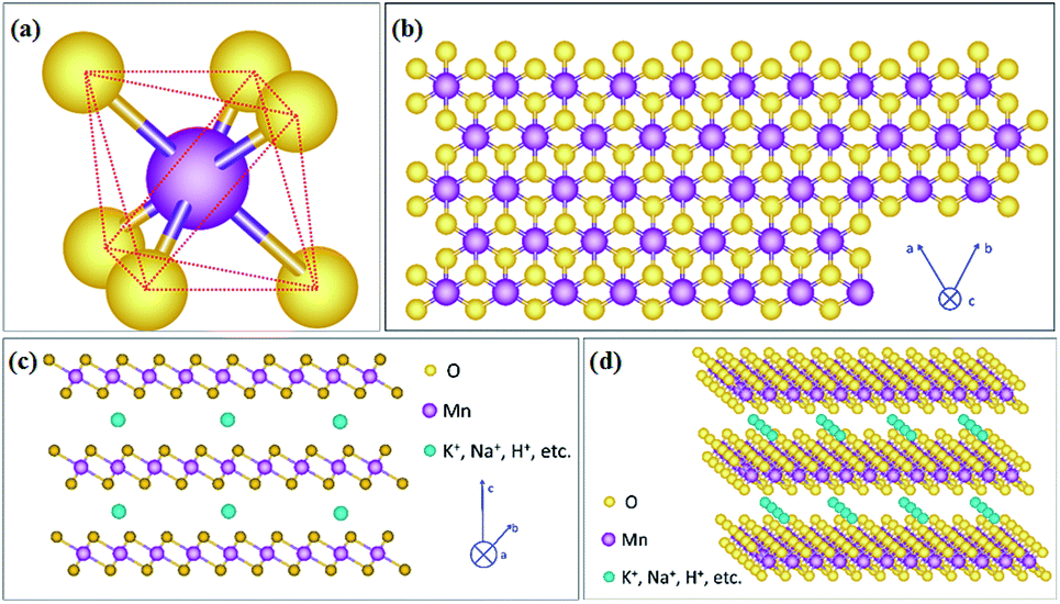 | ||
| Fig. 1 (a) MnO6 octahedron unit; (b) schematic diagram of birnessite along the 001 plane; (c) schematic diagram of birnessite viewed along the 011 plane; (d) stereoscopic schematic diagram of birnessite. | ||
Because of the layer structure feature, the XRD patterns (e.g. JCPDS: 80-1098; 86-0666) often exhibit diffraction peaks at around 12° and 25° corresponding to the interlayer spacing and half interlayer spacing (001 and 002 planes).65,66 Another two diffraction peaks often appear at around 36° and 66°, matching the 111 and 020 planes (Fig. 2a). These diffraction intensities depend on the crystalline degree and grain size. However, these diffraction peaks do not always belong to the 001, 002, 111 and 020 planes because of the existence of many subtype birnessites due to the different interlayer cationic species and variation of the interlayer (JCPDS: 86-0666; 18-0802; 23-1046; 27-0751; etc.). Because of the faster crystalline growth along the a and b axis compared to the c axis, the morphology of reported birnessite is often nanofilms or nanosheets, with an interlayer spacing of 0.24 nm and ∼0.7 nm corresponding to the distance between adjacent Mn atoms and interlayer spacing (Fig. 2b–d).67,68
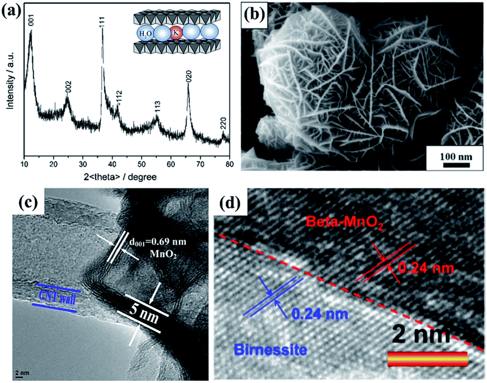 | ||
| Fig. 2 (a) Typical XRD pattern of birnessite.65 (b) SEM image of typical birnessite.67 (c) and (d) HRTEM images of typical birnessite.49,68 | ||
3. Energy storage mechanism of birnessite
The energy storage mechanism of birnessite based electrodes can be classified as a MnO2 electrode with both electrical double-layer capacitance (EDLC) and faradaic pseudocapacitance involved.18,69–72 Specifically, the EDLC is a kind of surface adsorption–desorption behavior existing in almost all of the electrodes. Similar to a parallel-plate capacitor, charge separation happens with a tight charge layer forming on the surface of birnessite based electrodes after being inserted into the electrolyte and an appropriate voltage was applied between these two electrodes.73–76 The EDLC can be estimated by referring to the following equation:| C = Aεrε0/d |
Another energy storage mechanism of birnessite based electrodes is pseudocapacitance coming from the valence state changes.77,78 During the charge–discharge process, the alkaline cations (Na+, K+, H+, etc.) in the electrolyte can be absorbed by the O atoms of the MnO6 octahedron because of the opposite electrical properties between alkaline cations and O atoms and then charges were transformed to the adjacent Mn atom whose valence changes from +4 to +3 as follows:
| (MnO2)surface + C+ + e− → (MnO2−C+)surface |
Apart from the above two mechanism, the energy storage mechanism of birnessite electrodes also contains an intercalation–deintercalation process.81,82 In this process, protons (H+) or alkali metal cations (C+) such as Li+ intercalate into the bulk of the material upon reduction followed by deintercalation from the bulk of the material upon oxidation as follows:
| MnO2 + C+ + e− → MnOOC |
| i = aνb |
![[thin space (1/6-em)]](https://www.rsc.org/images/entities/char_2009.gif) i vs. logν. A well-defined condition, b = 1.0, is representative of a capacitive response because the current is proportional to the sweep rate. The measured current from the surface capacitive contribution follows a linear law approximately because of the ultrafast reaction process, which is different from the diffusion-controlled contribution.85–87 A quantitative distinction of different capacitive contributions to the overall charge storage was provided based on the following equation:
i vs. logν. A well-defined condition, b = 1.0, is representative of a capacitive response because the current is proportional to the sweep rate. The measured current from the surface capacitive contribution follows a linear law approximately because of the ultrafast reaction process, which is different from the diffusion-controlled contribution.85–87 A quantitative distinction of different capacitive contributions to the overall charge storage was provided based on the following equation:| i(V) = k1v + k2v1/2 |
For analytical purposes, this equation was divided with the square root of the scan rate, then:
| i(V)/v1/2 = k1v1/2 + k2 |
In recent publications, high intercalated cation content birnessites were synthesized by adjusting the species of intercalated cations or oxidizing Mn3O4 crystals via an electrochemical oxidation method. Meanwhile, the energy mechanism of Mn based oxides with pre-inserted cations (alpha-MnO2 and birnessite) was revised as follows:89
Charge process:
| MxMnO2 → MnO2 + xM + xe− (M+ = H+, Na+, K+) |
Discharge process:
| MnO2 + xM + xe− → MxMnO2 (M+ = H+, Na+, K+) |
However, in this revised mechanism, the pseudocapacitance was misunderstood because the source of the pseudocapacitance was ignored. Actually, the energy storage process of birnessite based electrodes includes two steps. In the first step, once the birnessite based electrode, being a positive electrode, was immersed in the electrolyte together with a negative electrode, charge separation happens and an electric double layer forms. Meanwhile, the alkaline cations (Na+, K+, H+, etc.) in the electrolyte are absorbed by the O atoms of the MnO6 octahedron because of the opposite electrical properties between alkaline cations and O atoms and then charges were transferred to the adjacent Mn atom whose valence changes from +4 to +3. In the second step, these absorbed alkaline cations are released along with these pre-inserted cations during the charge process and consumed during the discharge process. Thus, not all the participating alkaline cations come from the pre-insertion process or component cations. Additionally, the energy storage process involved in the revised mechanism mainly comes from diffusion-controlled contribution rather than surface capacitive contribution. However, the capacitance of these prepared structures is enhanced a lot and the potential window was found to be increased to 1.2 V or even 1.3 V in an aqueous electrolyte because the potential window for K+ extracted is around 1.2 V. Based on these results, some high voltage asymmetrical supercapacitors (2.7–2.8 V) were assembled, which possess very high energy density.50,51
4. Challenges for birnessite based electrodes
In fact, at the present stage, the research hotspot is still the electronic conductivity of birnessite which influences the subsequent electrode reaction by gathering charges originating from electrochemical reactions. These gathered charges not only increase the operating potential windows within a short time resulting in an incomplete electrochemical reaction between birnessite and the electrolyte leading to a low capacitance, but also block the secondary response of active materials to the electrolyte generating a low rate capability. Introducing a conductive matrix into the birnessite based electrode is always a popular approach, but no great breakthroughs have been achieved yet. Note that the intrinsic conductivity of birnessite seems to be the key point, which determines the upper limit of birnessite based electrodes. Thus, charge transfer in the interior of birnessite should be taken into consideration.Another challenge is the balance of the crystalline degree of birnessite and its specific surface area. Many research studies have reported that it is very hard to achieve these two factors simultaneously, as a high crystalline degree means few defects in birnessite crystals, which means a low specific surface area. However, a higher crystalline degree will provide higher intrinsic conductivity for birnessite, which is very important for the electrode, while enhancing specific surface area is considered to be the most effective strategy to obtain high capacitance. Thus, some new projects aimed at enhancing the crystalline degree of birnessite and its specific surface area simultaneously should be proposed.
Finally, the component of birnessite should be taken into account. The theoretical capacitance of MnO2 is as high as 1370 F g−1. For some narrow tunnel MnO2 structures, like beta-MnO2, lambda-MnO2 and gamma-MnO2, the low obtained capacitance can be ascribed to the ultrahigh dead mass in the electrode as there is no room to store electrolyte ions in their bulk. However, for birnessite, most obtained capacitances still range from 200–400 F g−1, which is far below its theoretical capacitance. As we know, the theoretical capacitance of MnO2 is calculated based on the valence transition of Mn3+ to Mn4+, which happens in the whole operating potential window, while the capacitance of MnO2 is determined by the content of Mn4+, which will influence the adsorption capacity of electrolyte ions. Nevertheless, the content of Mn3+ in birnessite is around 33%. Although some results have demonstrated that the intrinsic electronic conductivity of birnessite can be enhanced by increasing the content of Mn3+, balancing the content of Mn3+ and the adsorbing capacity of birnessite is necessary.
5. Strategy of enhancing electrochemical properties
5.1 Enhancing conductivity
The electronic conductivity of active materials is often supposed to be one of the main factors affecting their electrochemical properties as charges originating from electrochemical reactions have to be transferred to an external circuit quickly, or these superfluous charges will impede further electrochemical reactions. The strategies for enhancing the electronic conductivity are often divided into two categories: one is introducing conductive materials to increase the total specific conductance of birnessite based structures; the other is improving the intrinsic conductivity of birnessite to overcome the weakness of electric conductivity.Graphene, as a two-dimensional, one atom thick and highly flexible carbon, has been widely used in electrodes, not only as an energy storage material but as a conductive supporting material, because of its high electrical conductivity (104 S cm−1), ultrahigh theoretical specific area (2630 m2 g−1) and excellent electrochemical stability.105 The high surface area and conductive graphene has the ability to accelerate the charge transfer and promote the reaction kinetics indeed during charge storage. Peng et al.106 have demonstrated that the energy storage process of the birnessite/graphene composite with a layer by layer structure should occur at the layer spaces and it is very hard or impossible for charges or ions to cross the graphene layer (Fig. 3a). The uniform distribution (Fig. 3b) and high crystalline degree birnessite (Fig. 3c) guarantees the layer-by-layer structure with high flexibility and high controllability. A planar supercapacitor (Fig. 3d) prepared by an etching method along the desired trajectory exhibits excellent rate capability with only 22% capacitance loss when the current density increases by a factor of 20 (from 0.5 to 10 A g−1) (Fig. 3e). Thus, a high energy density (18.64 W h kg−1) with a maximum power density of 12.6 kW kg−1 was obtained for this planar supercapacitor (Fig. 3f). As a flexible supercapacitor, the flexibility was tested in three physical states (flat, folded and rolled), and a very similar capacitance was obtained for these three states (Fig. 3g). Additionally, over 90% of the capacitance was retained for the device after being folded thousands of times (Fig. 3h). These results highlighted the high electronic conductivity and flexibility of graphene which can be inherited by birnessite/graphene composites to generate special electrodes.
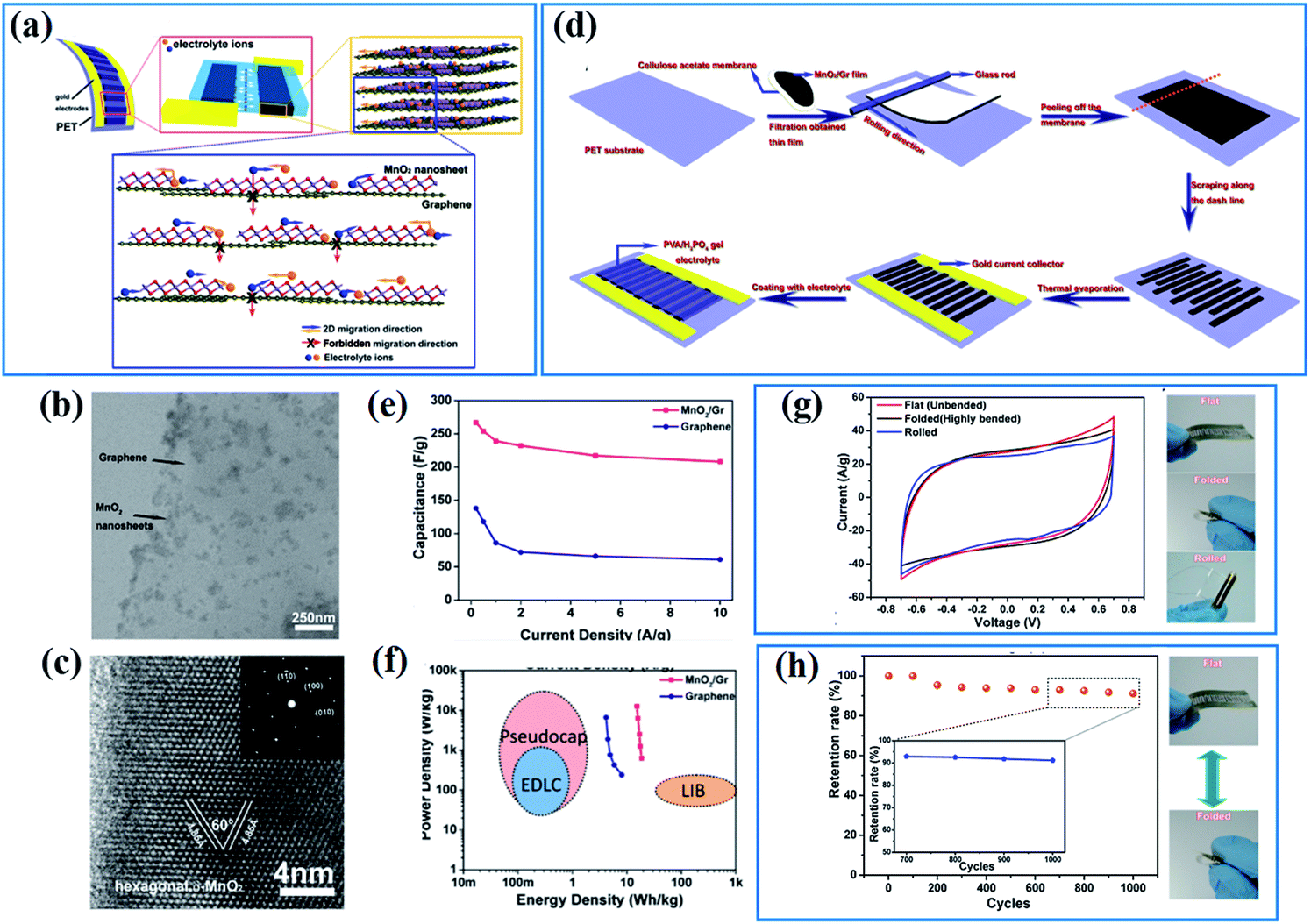 | ||
| Fig. 3 (a) Design of hybrid 2D birnessite/graphene structure based planar supercapacitors; (b and c) TEM images of the 2D hybrid structure with birnessite nanosheets integrated on graphene surfaces; (d) schematic of fabrication procedures for ultraflexible planar supercapacitors; (e) comparison of specific capacitance values for the hybrid supercapacitors and those based on graphene. (f) A typical Ragone plot of the as-fabricated supercapacitors. (g) CV curves of the planar supercapacitor under three different bending states and demonstration of three different bending states: flat, folded, and rolled; (h) cycling stability under repeated flat/folded cycles and demonstration of the flat/folded cycle when testing cycling stability.106 | ||
Compared to graphene, carbon nanotubes (CNTs) are a 1D highly crystalline tubular carbon with a diameter of several tens of nanometers, which possess very high electronic conductivity, high mechanical strength and high chemical stability providing an effective charge transfer route. Additionally, the surface properties of multiwalled carbon nanotubes can be changed by various methods without decreasing their electronic conductivity markedly, which ensures more approaches to fabricate birnessite/CNT composites. Wu and co-authors107 reported self-standing and highly flexible δ-MnO2@CNTs/CNT composite films using a three step strategy (Fig. 4a). The CNTs were prepared through a CVD process and used as the substrate to load birnessite with the surface of these CNTs changing from smooth to rough (Fig. 4b and c). The self-standing flexible films were obtained by a vacuum filtration method with CNTs and birnessite/CNT composites applied alternately (Fig. 4d). Thus, these free-standing electrodes are supposed to have excellent electrochemical properties. There is only about 15% fading of the capacitance when the discharge current increased from 0.2 A g−1 to 5 A g−1 (Fig. 4e). Additionally, the specific capacitance remains almost unchanged with the mass of the electrode increasing from 1.97 to 6.18 mg cm−2 and the area capacitance increasing linearly, indicating the high porosity and high conductivity of these self-standing film electrodes (Fig. 4f and g), while both the specific capacitance and volumetric capacitance remain unchanged with the diameter of the electrode increasing. Moreover, the specific capacitance was slightly reduced with the bending angle applied from 0 to 180° (Fig. 4h). These results highlighted the outstanding mechanical properties and excellent electrochemical performance, as well as easy processing of birnessite/CNT free standing electrodes.
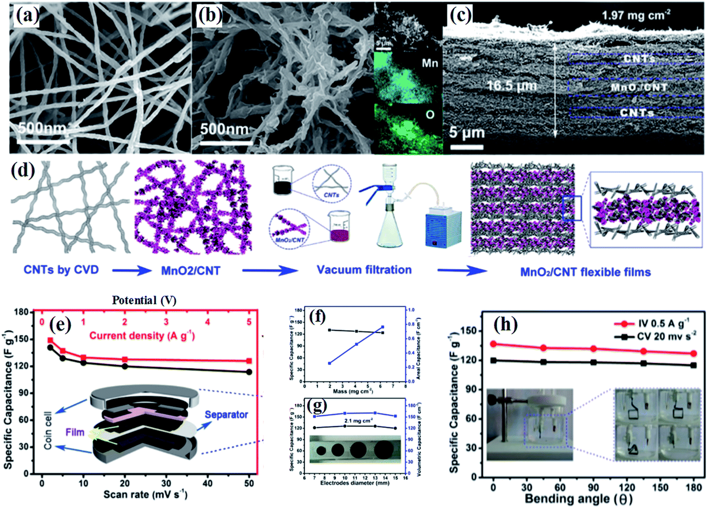 | ||
| Fig. 4 (a and b) SEM images of raw CNTs; SEM images of birnessite@CNT composites, insets show the EDS elemental mapping images, showing the spatial distribution of Mn and O; (c) cross section of a unit of the birnessite@CNTs/CNT stacked film with a thickness of 16.5 μm; (d) schematic of the preparation process of stacked films; (e) dependence of specific capacitance on the scan rate (bottom axis) and on the current density (top axis) determined from the CV curves and GCD curves, respectively; (f) mass (left axis) and areal (right axis) specific capacitance as a function of the areal mass of the flexible films calculated from the GCD curve; (g) dependence of mass (left axis) and volumetric specific capacitance (right axis) on the diameter determined from the discharge curves at 0.5 A g−1. A photograph of the flexible electrodes with different diameters (inset); (h) specific capacitance change with bending angles calculated from the CV curves (black) and GCD curves (red). The inset shows photographs of the three-electrode configuration.107 | ||
Besides conductive carbon species, highly conductive metals are also a favorable additive used for supporting birnessite. These conductive metals should possess high chemical inertness which ensures a stable and highly conductive substrate. Among all the conductive metals, Au is the most attractive material due to its high electronic conductivity and high ductility, which may not only provide the electrode with high electrochemical performance but some special physical properties as well. Qiu et al.108 reported a template method using PS spheres as a sacrificial template to fabricate a Au@birnessite nanomesh (Fig. 5a(i)). Au was used not only as a substrate to support birnessite but also as a conductive path for charges (Fig. 5a(ii)). Additionally, the uniform pores originating from the sacrificial PS spheres facilitate ion transfer (Fig. 5a(iii and iv)). Thus, excellent rate capabilities were obtained for this structure (Fig. 5a(v)). When connecting two devices together, a perfect superimposed charge–discharge curve was obtained (Fig. 5a(vi)). The excellent electrochemical properties are surely ascribed to the high electronic conductivity of Au, which was inherited by the Au@birnessite nanomesh. Zhu and co-authors109 coupled mesoporous gold with birnessite, which ensures a high electronic conductivity and fast ion transition (Fig. 5b(i–iii)). These mesoporous gold@birnessite nanostructures can be pressed into an electrode directly without any extra current collectors due to the high ductility of Au (Fig. 5b(iv)). The electrode exhibited a high capacitance of 906.4 F g−1 and good rate capability because of the high conductivity originating from mesoporous gold (Fig. 5b(v and vi)).
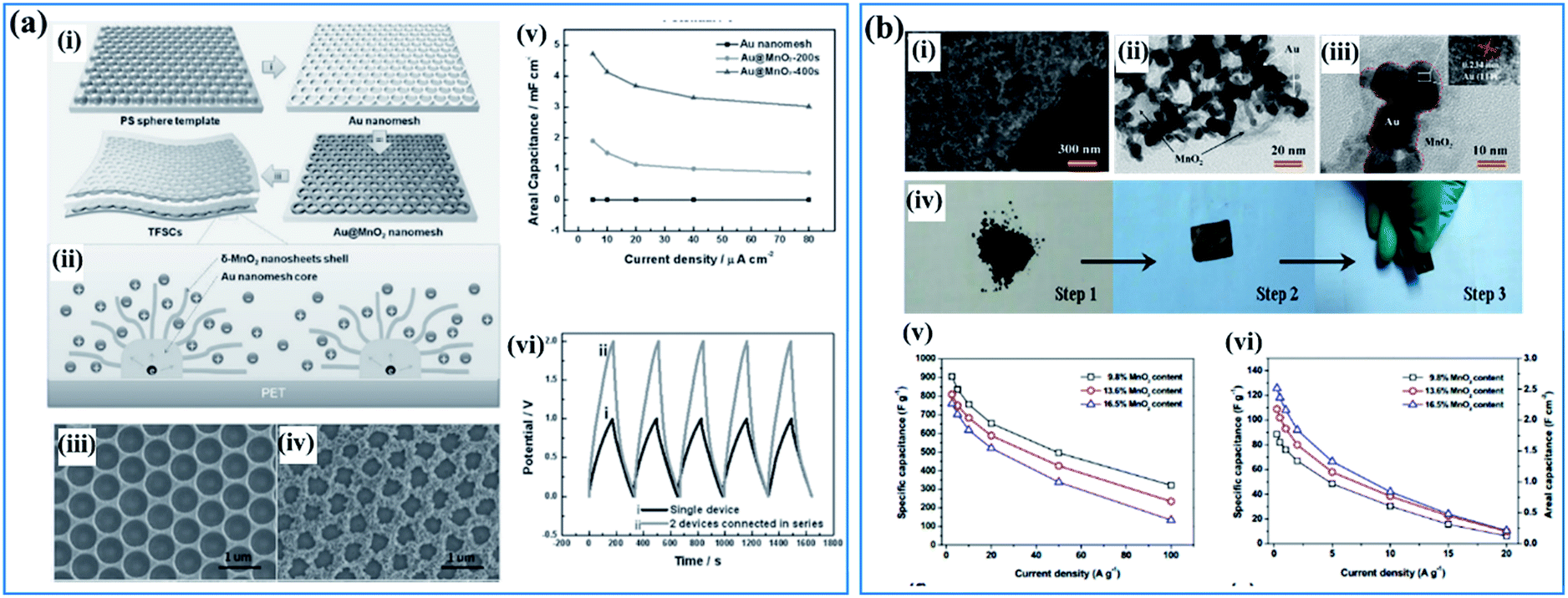 | ||
| Fig. 5 (a) Au@birnessite core–shell nanomesh: (i) schematic illustration of the fabrication of the Au@birnessite nanomesh-based TFSC; (ii) schematic diagram of ion diffusion pathways and charge transport channels of the Au@birnessite nanomesh electrode; (iii) SEM image of the Au nanomesh; (iv) SEM image of the Au@birnessite core–shell nanomesh peeled from the PET substrate; (v) the areal capacitance of the Au nanomesh, Au@birnessite–200s and Au@birnessite–400s as a function of the current density; (vi) the galvanostatic charge/discharge curves of a single device and 2 devices connected in series at 5 μA cm−2.108 (b) Mesoporous gold networks@birnessite: (i) FIB/SEM image of the Au@birnessite network (16.5 wt% birnessite); (ii, iii) TEM images of the Au@birnessite network (16.5 wt% birnessite); (iv) the preparation process of the electrode; (v) specific capacitances of Au@birnessite networks at different current densities based on the weight of birnessite; (vi) specific capacitances of the Au@ birnessite network at different current densities based on the whole weight of the electrode.109 | ||
Although the electronic conductivity of birnessite based composites can be improved by introducing exterior conductive species and the rate capacitance was enhanced obviously, the capacitance still lies in a low level if high mass loading birnessite was applied. Note that the conductivity of materials always followed a “short slab” principle for a single conducting path. Thus, the intrinsic conductivity of birnessite should not be ignored.
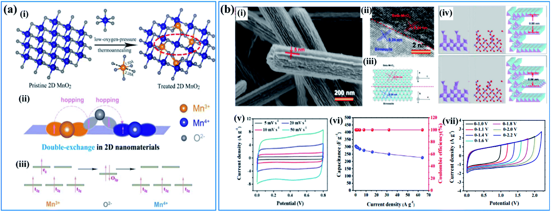 | ||
| Fig. 6 (a) Double-exchange mechanism in birnessite: (i) diagram of low-oxygen-pressure thermo-annealing treatment to achieve double-exchange of Mn(III)–O–Mn(IV) in the treated birnessite nanosheet. (ii, iii) Double-exchange of Mn(III)–O–Mn(IV) results in magnetoresistance in the 2D birnessite nanosheets.110 (b) β-MnO2/parallel birnessite core/shell nanorod: (i) SEM image of β-MnO2/parallel birnessite core/shell nanorods; (ii) high resolution TEM image of a β-MnO2/parallel birnessite core/shell nanorod; (iii) structural representation of a β-MnO2/parallel birnessite core/shell nanorod (perpendicular to the 001 plane of parallel birnessite); (iv) structural computation of a β-MnO2/parallel birnessite core/shell nanorod (formation 1 and formation 2); (v) cyclic voltammograms at different scan rates (potential window: 0–0.8 V); (vi) variations of the capacitance and coulombic efficiency with the current densities (potential window: 0–0.8 V); (vii) CV curves of β-MnO2/parallel birnessite//AGO ASC at different cell voltages at a scan rate of 50 mV s−1.49 | ||
Based on the “double-exchange” mechanism, the intrinsic resistance of birnessite was reduced by increasing the content of Mn3+ within limits, which will influence its electrochemical properties markedly. Zhu et al.49 reported structural directed growth of ultrathin parallel birnessite on β-MnO2 with birnessite standing on the surface of β-MnO2 parallelly (Fig. 6b(i)) and a high Mn3+ content. The crystal structure of the as-prepared birnessite changed slightly because of the restriction of the crystal lattice of beta-MnO2, which enhanced the electrochemical properties (Fig. 6b(ii–iv)). Birnessite displayed a regular box-like shape and an ultrahigh capacitance of 657 F g−1 based on the weight of parallel birnessite and 306 F g−1 based on the whole weight of the nanocomposite in 1 M Na2SO4 electrolyte (Fig. 6b(v)). Additionally, excellent rate capability was found as the conductivity of this nanostructure improved a lot, which can be ascribed to the increased content of Mn3+. Thus, approximately 74% of the capacitance was retained when the current density increased from 0.25 A g−1 to 64.0 A g−1 (Fig. 6b(vi)). A device assembled with the as-prepared nanostructure as the positive electrode and reduced graphene oxide as the negative electrode gives a high energy density of 40.4 W h kg−1 at a power density of 275 W kg−1 as the potential window of the device was increased to 2.2 V (Fig. 6b(vii)).
Although the electronic conductivity was improved because of the increased content of Mn3+ and the dead mass of birnessite was reduced because of the unique structure and ultrathin birnessite films, the dead mass of the whole structure increased as beta-MnO2 was introduced, which contributed little to the capacitance, resulting in a very high capacitance based on the weight of birnessite but ordinary capacitance based on the weight of the whole mass of the structure. However, a new idea of enhancing the electrochemical properties of birnessite was put forward and can be optimized further.
A detailed investigation of Fe-doped birnessite including crystallinity, morphology, valence states, crystal structure, electronic structure, conductivity and electrochemical performance was proposed by Tian's group.114 Specifically, the crystalline degree of Fe-doped birnessite become poorer and poorer (Fig. 7a) and the average particle sizes become smaller and smaller (Fig. 7b) with the increase of the amount of the Fe dopant. These can be ascribed to the formation of defects (e.g. vacancies) and distortions, which can hinder crystal growth in the host structure after Fe doping. Moreover, the relative percentage of Mn(III) decreases progressively as the content of the Fe dopant increased (Fig. 7c), confirming that Mn(III) was substituted by Fe(III) in the doped birnessite samples. The electron charge density of Fe-doped birnessite exhibits an enlarged Fe–O bond (2.086 Å) compared with the Mn–O bond (2.060 Å) because of the ionic character of Fe atoms (Fig. 7d), resulting in a metabolic electronic structure of birnessite. Thus, the band gap of birnessite can be reduced after Fe doping as revealed by DFT calculations, leading to the increase of the intrinsic electronic conductivity of doped-birnessite (Fig. 7e). Hence, an enhanced rate capability related to the electronic conductivity of birnessite was found (Fig. 7f).
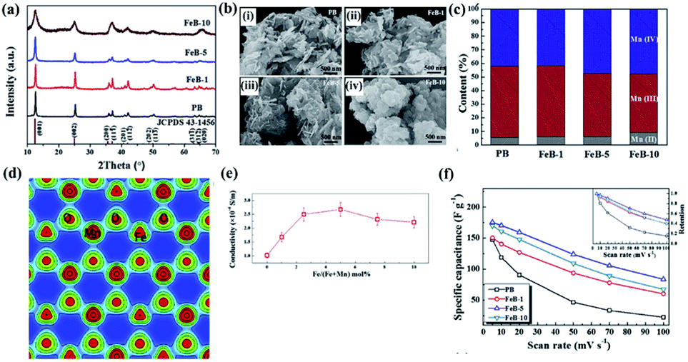 | ||
| Fig. 7 (a) XRD patterns of PB, FeB-1, FeB-5, and FeB-10 samples; (b) SEM images taken from PB, FeB-1, FeB-5, and FeB-10 samples; (c) the relative content of Mn(II), Mn(III) and Mn(IV) in these prepared samples calculated from the corresponding XPS spectral fitting; (d) electron charge density distribution of Fe-doped birnessite with 33.3 mol% Fe content viewed along the (001) plane; (e) electrical conductivities of the prepared birnessite samples changing with the molar percentage of Fe; (f) comparison of the specific capacitances of PB, FeB-1, FeB-5 and FeB-10 samples at different scan rates. The inset shows capacitance retention of these samples at different scan rates.114 | ||
These results demonstrate the ion transport kinetics, electron structure and crystal structure can be altered by doping with heteroatoms to some extent. However, the variation of these properties is not always benin. Suitable heteroatoms should be selected by first-principles calculations as some heteroatoms may destroy the original electronic conductive path. Additionally, metal doped birnessite may have optimized conductivity and reaction kinetics resulting in enhanced electrochemical properties, which calls for atomic-scale and highly dispersive doping. Some in situ studies on the intrinsic reaction process and the interaction mechanism between the doped atoms and MnO2 also provide a lot of inspiration to construct high-performance electrodes.
5.2 Crystal dimensional regulation
Despite the high specific surface area and abundant electrochemically active sites, the electrical conductivity of birnessite is pretty low, compared to other crystal type Mn-based oxides, because of the high content of crystal water, sparse atoms and poor crystalline degree, resulting in a large amount of dead mass in birnessite based electrodes which cannot be used for energy storage. Thus, reducing the dead mass in birnessite based electrodes is always the greatest demand for enhancing the energy density of supercapacitors. Many strategies have been developed to reduce the crystalline size to reduce the dead mass or increase the utilization ratio of birnessite, thus providing some superiority for supercapacitor application.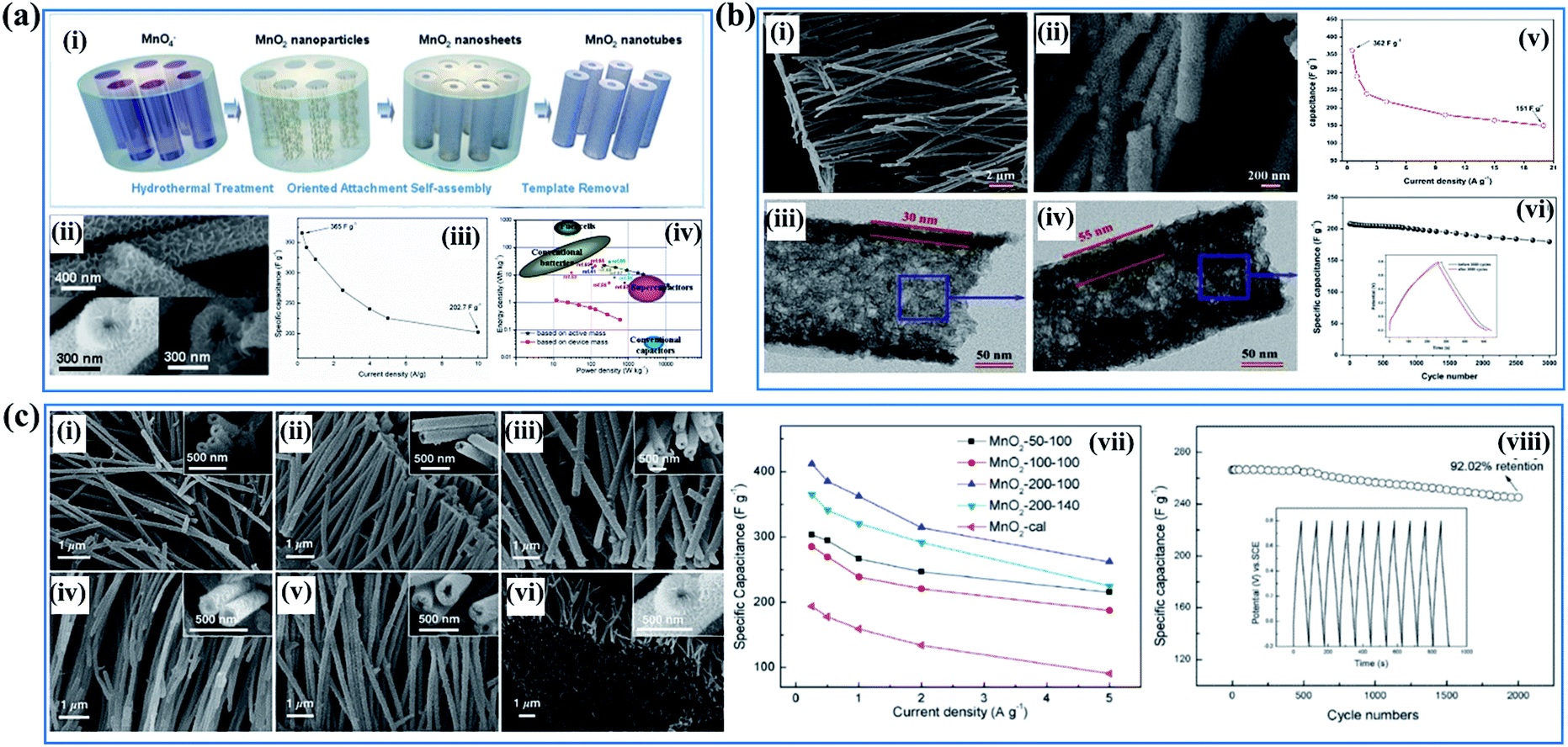 | ||
| Fig. 8 (a) Porous birnessite nanotubes: (i) schematic illustration of the procedure to synthesize porous birnessite nanotubes; (ii) SEM images of birnessite nanotubes; (iii) specific capacitance of birnessite nanotubes measured under different current densities; (iv) (e) the energy density vs. power density of the birnessite nanotubes//AG asymmetric supercapacitor.33 (b) Coaxial double nanotubes: (i, ii) SEM and TEM images of coaxial double nanotubes with inner birnessite and outer amorphous carbon; (iii and iv) SEM and TEM images of coaxial double nanotubes with outer birnessite and inner amorphous carbon; (v) specific capacitance of coaxial double nanotubes with outer birnessite and inner amorphous carbon measured under different current densities; (vi) variations of capacitance with cycle numbers for coaxial double nanotubes with outer birnessite and inner amorphous carbon with insets showing the comparison of galvanostatic charge–discharge curves before and after 3000 cycles.125 (c) Porous birnessite tubular arrays: SEM images of birnessite nanotubes: (i) birnessite-50–100, (ii) birnessite-100–100, (iii) birnessite-200–100, (iv) birnessite-50–140, (v) birnessite-100–140, and (vi) birnessite-200–140; (vii) specific capacitance under different current densities; (viii) cycling performance of birnessite-200–100 at a current density of 5 A g−1. The inset shows the charge–discharge curves of the last 10 cycles of the MnO2-200–100 electrode.126 | ||
For sphere-like hollow structures and specific template-like structures, the main preponderance is that the morphologies of these structures are easy to be controlled and can be scaled up as templates are often applied in these strategies.128–131 These structures often possess high specific capacitance and good rate capability as the hollow structure can be used as a transit depot for the electrolyte, which shortens the ion transfer distance. Zhang et al. reported a yolk and hollow structure assembled with ultrathin birnessite films which gives a high specific capacitance of 273 F g−1 with good rate capability. In this structure, colloid carbon spheres were used as the sacrificial template which can be adjusted by controlling the pH values of the reaction solution.132 Munaiah et al. prepared hollow birnessite spheres assembled from ultrathin birnessite films with a very poor crystalline degree by a soft template method. The hollow sphere displayed a capacitance of 283 F g−1 in 0.1 M Ca(NO3)2 solution. However, the cycling stability of this structure is very poor with 37% of its initial capacitance being lost after 1000 cycles, which may be because the hollow sphere was crushed during the charge–discharge process.133 In recent years, some studies reported using biological materials as the template to support ultrathin birnessite for supercapacitors as some biological materials possess unique pores which are considered to be one of the most important factors affecting their electrochemical properties. Zhang's group reported many studies on ultrathin birnessite films and diatomite which exhibited outstanding electrochemical properties including high specific capacitance and excellent rate capability.38,134–136 However, most of the studies did not give very good cycling stability, which can be ascribed to the crushing of active materials during the testing process.
Although the specific capacitance of birnessite has been improved a lot by these strategies, the electronic conductivity of the obtained birnessite structure had not been enhanced resulting in poor rate capability. Additionally, the dimensionality of these structures is designed to be smaller and smaller leading to poor mechanical strength, which influences the cycling stability to a great extent.
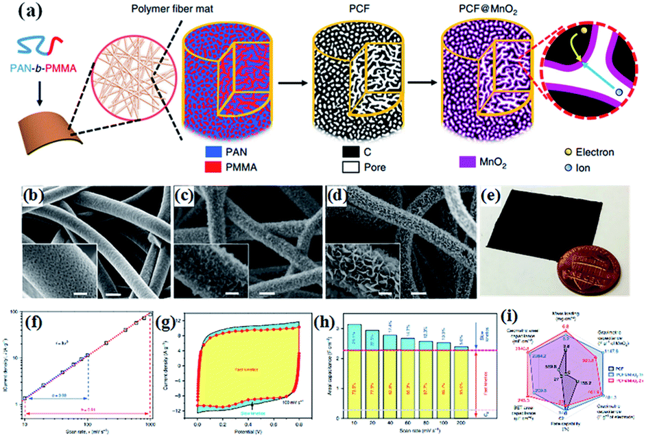 | ||
| Fig. 9 (a) Schematic illustration of the synthesis of PCF and PCF@birnessite; SEM images of (b) PCF, (c) PCF@birnessite-1h, and (d) PCF@birnessite-2h; (e) a photograph of a piece of the PCF@birnessite-2h electrode next to a U.S. penny with a diameter of ∼1.9 cm; (f) absolute current density and scan rate follow the power law, i = kvb, in both the slow and fast scan rate regions; (g) decoupling of the capacitance contributed by the fast-kinetic processes (yellow) and the slow-kinetic processes (blue); (h) histograms of the capacitance contributions by the different processes: yellow, fast-kinetic processes; blue, slow-kinetic processes; Cdl, electrical double layer capacitance; (i) the radar chart compares six figures-of-merit of PCF (black), PCF@birnessite-1h (blue), and PCF@birnessite-2h (red): mass loading of the active materials, rate capability (from 10 to 1000 mV s−1), gravimetric capacitance based on the mass of birnessite and active materials, and areal capacitance based on the geometric area and BET surface area. All capacitances are obtained at 10 mV s−1.104 | ||
5.3 Defect engineering
Recent studies have shown that the conductivity and charge storage can be effectively improved by introducing anion or cation vacancies into birnessite because of the promoted surface redox reaction kinetics resulting in an enhanced electrochemical performance.141–143 Especially, for birnessite with oxygen vacancies, the oxygen vacancies would lead to charge compensation by changing the oxidation states of Mn ions (Mn2+, Mn3+, and Mn4+) in birnessite, which will further result in variation of the charge carrier density and make the deficient birnessite more conductive.144 Additionally, oxygen vacancies are capable of providing additional ion intercalation sites to effectively improve the specific capacitance of birnessite. Gao et al.145 reported birnessite with Mn vacancies with a controllable amount of vacancies by reassembling the as-exfoliated birnessite at different pH values. The flocculated nanosheet samples exhibit 3D porous nanostructures and equilibration at different pH values has no influence on their morphologies (Fig. 10a–c). XANES spectra of protonated birnessite exhibit a higher intensity of P′, where the weak pre-edge peaks P and P′ correspond to the dipole-forbidden 1s–3d transition, indicating the coexistence of Mn3+ and Mn4+ (Fig. 10d). Moreover, a negative shift of the main absorption peaks with the decrease of pH values was found after taking the derivative of XANES spectra, indicating that lower pH progressively reduces Mn to the trivalent state (Fig. 10e). Additionally, high-energy X-ray scattering and pair distribution function analysis were performed to characterize the content of Mn vacancies. Two main pair distribution function peaks, the in-plane Mn–Mn peak at 2.89 Å and the Mn–Mnsurf distance at 3.45 Å, related to the content of Mn vacancies were considered (Fig. 10e). The content was calculated to be 18.3% at pH <1, 26.5% at pH = 2 and 19.9% at pH = 4 because of Jahn–Teller distortion, and may be accommodated in crystalline birnessites (Fig. 10f). Based on these results, the as-prepared Mn vacancy birnessite delivered a greatly enhanced capacitance value of over 300 F g−1 (1 M Na2SO4 electrolyte) and improved cycling performance.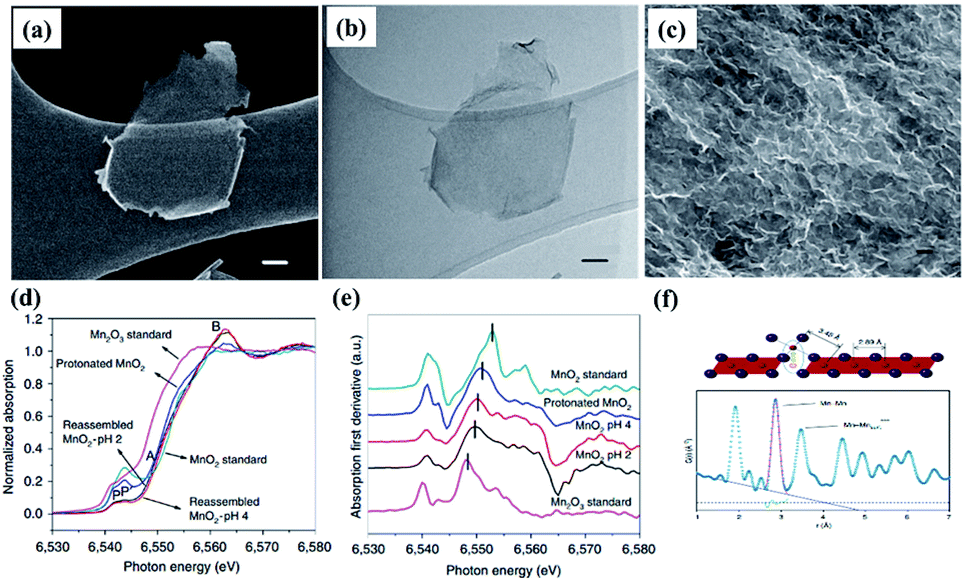 | ||
| Fig. 10 (a) SEM image and (b) bright-field TEM image of exfoliated birnessites, scale bar, 50 nm; (c) SEM image of reassembled birnessite nanostructures treated in pH = 2 solution for 24 h, scale bar: 500 nm; (d) XANES spectra of protonated birnessite, pH = 2 and 4 treated reassembled birnessite; (e) first derivative curves corresponding to the samples; (f) models of in-plane Mn–Mn and Mn surface and pair distribution function analysis of reassembled birnessite.145 | ||
5.4 Synergistic effect
In recent years, many articles have demonstrated that the electrochemical properties of birnessite can be enhanced by introducing another one or two components into birnessite based materials and the electrochemical performance of the introduced components can also been improved, which can be ascribed to the changing of the charge transfer route, interaction of the same involved ions or heterojunction enhanced electrical performances.16,146–153 In well-designed materials, the dead mass of birnessite was decreased because the utilization of birnessite was enhanced, resulting in improved capacitance, rate capability and cycling stability. Zhu et al. reported CeO2@birnessite core–shell heterostructures using both CeO2 octahedra and nanowires as the cores to support birnessite (Fig. 11a(i–vi)). These CeO2 nanowire@birnessite nanostructures exhibited unprecedented pseudocapacitance performance (255 F g−1) with outstanding rate capability and high energy density (Fig. 11a(vii and viii)). A new mechanism for the enhanced rate capability has been proposed. Specifically, during the electrochemical test, the CeO2 cores act as an accelerator. In the process of oxidation, CeO2 and birnessite release their electron at the same time due to the mandatory potential difference. However, the high activity of CeO2 makes it easy to be oxidized and reduced during the oxidation–reduction process. Thus, CeO2 depopulates the electrons from MnO2 uninterruptedly which enhances the degree of oxidation of birnessite resulting in an enhanced electrochemical performance and vice versa. However, such approaches often suffer from poor electronic conductivity of these inorganic nanomaterials.154 Jiang and co-authors46 reported the synergistic effect of birnessite and polyaniline with K-birnessite grown on the surface of polyaniline (Fig. 11b(i–iv)). The as-prepared PANI–birnessite coaxial nanofibers with optimal composition, when applied as an electrode, exhibited a high specific capacitance (383 F g−1 at 0.5 A g−1) with a good rate in 1 M Na2SO4 aqueous solution, which is attributed to the synergistic effects of the combined pseudo-capacitive contributions from the core and shell (Fig. 11b(v)).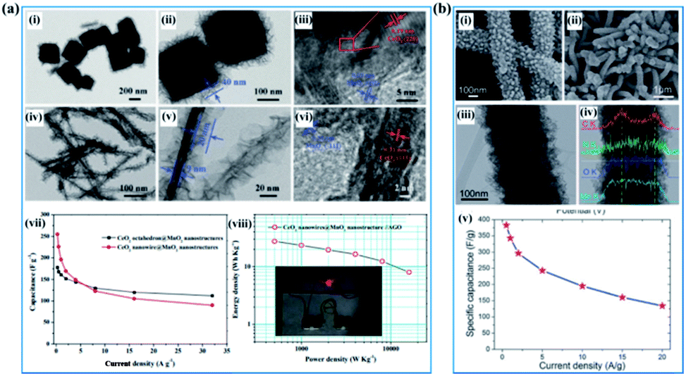 | ||
| Fig. 11 (a) CeO2@birnessite core–shell heterostructures: (i–iii) TEM images of the CeO2 octahedron@birnessite nanostructure; (iv–vi) TEM images of the CeO2 nanowire@birnessite nanostructure; (vii) specific capacitance under different current densities; (viii) Ragone plots of the CeO2 nanowire@birnessite nanostructure//active graphene oxide (AGO) asymmetric supercapacitor. The inset shows the digital image of a red light-emitting diode (LED) lit by the as-prepared device.154 (b) PANI–birnessite coaxial nanofibers: (i, ii) SEM image of PANI nanofibers; (ii) low- and high-magnification SEM images; (iii) TEM images (inset shows the SAED pattern); (iv) line-scanning (indicated by a white line) of the PANI–birnessite coaxial nanofibers; (v) the specific capacitance as a function of different current densities.46 | ||
There are also lots of papers reporting the “synergistic effect” of birnessite and other metal oxides,39,41,68,155–157 metal hydroxides,158–161 metal sulfides,162,163 or layered double hydroxides (LDHs),87,164–166 which enhanced the electrochemical properties by reducing the dead mass of birnessite. Liu et al. reported Co3O4 nanowire@MnO2 (birnessite) ultrathin nanosheet core/shell arrays by a three-step hydrothermal method (Fig. 12a). These nanocomposites exhibit not only high specific capacitance (480 F g−1), but also high areal capacitance (0.56 F cm−2). Additionally, the cycling stability was also improved (97.3% retention after 5000 cycles). The combination of MnO2 and Co3O4 with a unique morphology and independent electroactivities into a single engineered hierarchical architecture can substantially enhance the electrochemical properties.155 Soon afterwards, Kong and co-authors167 refined this structure and an ultrahigh capacitance of 1693.2 F g−1 and an excellent long-term electrochemical stability with only 10.2% capacitance loss after 5000 cycles were obtained (Fig. 12b). Based on these results, Huang et al.68 prepared a similar Co3O4 nanowire@MnO2 (birnessite) composite by a two-step hydrothermal method, which also exhibited high capacitance (560 F g−1) and excellent cycling stability (95% retention after 5000 cycles) (Fig. 12c). In these kinds of nanostructures, the bulk birnessite is replaced by metal oxides which not only ensures that the remaining birnessite can be fully used for energy storage, but also provides a transfer route for charges as the conductivity of Mn-based materials (1 × 10⁻⁶ S m−1) is pretty low compared to that of most metal oxides (1 × 10⁻⁵–1 × 10⁻⁴ S m−1). However, the applied electrolyte is a big problem for these structures and many electrolytes, including 1.0 M Na2SO4, 1.0 M LiOH and 6.0 M KOH, have been tested. However, it is very hard to choose an optimal electrolyte for these two components. For 1.0 M Na2SO4 electrolyte, which is very suitable for birnessite, almost no capacitance can be originated for other metal oxides, like NiO, Ni(OH)2, Co3O4, NiCoO2, LDH, etc. While, if 1.0 M LiOH or 6.0 M KOH was used, the electrochemical performance of birnessite was reduced a lot and these embedded metal oxides also cannot exhibit their full capacitance because of inadequate contact with the electrolyte as they were covered with birnessite. As a consequence, the capacitance calculated for these composites is always lower than that of the embedded metal oxide, while the capacitances calculated based on the weight of birnessite are very high, which means that the dead mass of birnessite can be reduced efficiently by introducing embedded metal oxides.
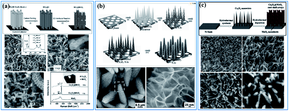 | ||
| Fig. 12 (a) Co3O4 nanowire@birnessite ultrathin nanosheet core/shell arrays.155 (b) Co3O4@birnessite hierarchical nanoneedle arrays.167 (c) Hierarchical Co3O4@birnessite core–shell arrays.68 | ||
To well present the uniqueness and difference of these strategies to adjust the electrochemical performance of birnessite based electrodes, their generated electrochemical properties are summarized systematically in Table 1. Generally speaking, the current results are far away from practical requirements.
| Strategy | Active materials | Capacitance | Rate capability | Cycling stability | Electrolyte | Ref. |
|---|---|---|---|---|---|---|
| Enhancing conductivity | 2D birnessite/graphene hybrid nanostructures | 267 F g−1 at 0.2 A g−1 | 78 (0.2 to 10 A g−1) | 92% (after 7000 cycles) | PVA/H3PO4 | 106 |
| Birnessite@CNTs/CNTs composite | 149 F g−1 at 0.2 A g−1 | 85% (0.2 to 5 A g−1) | 90% (after 5000 cycles) | 1 M Na2SO4 | 107 | |
| Au@birnessite core–shell nanomesh | 4.72 mF cm−2 at 5 μA cm−2 | 63.7% (5 to 80 μA cm−2) | 95% (after 1000 cycles) | 1 M Na2SO4 | 108 | |
| Mesoporous gold networks@birnessite | 906.4 F g−1 at 2.5 A g−1 | 72.2% (2.5 to 20 A g−1) | 97.2% (after 5000 cycles) | 1 M Na2SO4 | 109 | |
| Parallel birnessite/β-MnO2 | 306 F g−1 at 0.25 A g−1 | 74 (0.25 to 64 A g−1) | 92% (after 3000 cycles) | 1 M Na2SO4 | 49 | |
| Vanadium doped birnessite | 246 F g−1 at 0.2 A g−1 | 85 (0.2 to 1.6 A g−1) | NA | 1 M Na2SO4 | 48 | |
| Fe doped birnessite | 175.6 F g−1 at 5 mV s−1 | NA | 110 F g−1 (after 6000 cycles) | 1 M Na2SO4 | 114 | |
| Molybdenum-doped birnessite microspheres | 202 F g−1 at 0.1 A g−1 | 65.3 (0.1 to 2 A g−1) | 90% (after 2000 cycles) | 1 M Na2SO4 | 115 | |
| Crystal dimensional regulation | Birnessite nanoflowers | 197.3 F g−1 at 1.0 A g−1 | 64.3% (1.0 to 10 A g−1) | 94.6% (after 1000 cycles) | 1 M Na2SO4 | 120 |
| Mesoporous birnessite nanotubes | 365 F g−1 at 0.25 A g−1 | 55% (0.25 to 10 A g−1) | 90.4% (after 3000 cycles) | 1 M Na2SO4 | 168 | |
| Coaxial mesoporous birnessite/aCNT nanotubes | 362 F g−1 at 0.5 A g−1 | 41.7 (1.0 to 20 A g−1) | 88.6% (after 3000 cycles) | 1 M Na2SO4 | 125 | |
| Birnessite hollow sphere | 188 F g−1 at 0.5 mA cm−2 | 52% (0.5 to 10 mA cm−2) | 63% (after 1000 cycles) | 0.1 M Ca(NO3)2 | 133 | |
| PCF@birnessite | 481.3 F g−1 at 10 mV s−1 | 57% (10 to 200 mV s−1) | 98% (after 5000 cycles) | 6 M KOH | 104 | |
| Defect engineering | 3D porous birnessite nanosheet | 306 F g−1 at 0.2 A g−1 | ∼40% (0.2 to 10 A g−1) | 92% (after 1000 cycles) | 1 M Na2SO4 | 145 |
| Mixed-valence birnessite | 2530 F g−1 at 0.61 A g−1 | 96 (0.61 to 122.7 A g−1) | NA | 1 M Na2SO4 | 142 | |
| Synergistic effect | CeO2@birnessite core–shell heterostructures | 255 F g−1 at 0.25 A g−1 | 62.9 (0.25 to 32 A g−1) | 90.1% (after 3000 cycles) | 1 M Na2SO4 | 154 |
| Polyaniline–birnessite coaxial nanofiber | 383 F g−1 at 0.5 A g−1 | 35 (0.5 to 20 A g−1) | 75.5% (after 2000 cycles) | 1 M Na2SO4 | 46 | |
| Co3O4 nanowire@birnessite nanosheet arrays | 480 F g−1 at 2.67 A g−1 | 56 (4 to 44.7 mA cm−2) | 97.3% (after 5000 cycles) | 1.0 M LiOH | 155 | |
| Co3O4@birnessite hierarchical nanoneedle arrays | 1905.4 F g−1 at 0.5 A g−1 | 43.2 (0.5 to 10 A g−1) | 89.8% (after 5000 cycles) | 1.0 M LiOH | 167 | |
| Hierarchical Co3O4@birnessite core–shell arrays | 560 F g−1 at 0.2 A g−1 | 54.5 (0.2 to 10 A g−1) | 95% (after 5000 cycles) | 1.0 M LiOH | 68 |
6. Future prospects
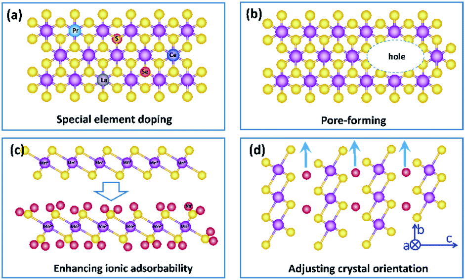
In summary, birnessite based structures are still one of the most promising materials for supercapacitors, and a recent trend in research is to develop birnessites with high conductivity, abundant electrochemically active sites and high utilization rate to reduce the gathering charges, enhance electrochemical reaction sites and reduce dead mass. Benefitting from these integrated advantages, with excellent pseudocapacitive properties, super-high theoretical capacitance and a large voltage window, the supercapacitors fabricated from birnessite are highly desired in energy storage systems with high energy/power density. However, there is still a big gap between the obtained properties and that of available practical electrodes. To overcome this gap, although scientific researchers focus on the regulation of the specific surface area, morphology and conductivity, there are still lots of possibilities in crystalline control, affinity of the electrolyte, special element doping and pore formation to enhance their electrochemical properties. Thus, several possible strategies to further enhance the high electrochemical performance of birnessite based structures for supercapacitor electrodes are listed below:(i) Increasing the intrinsic electronic conductivity of birnessite. As we discussed above, the electronic conductivity of birnessite is one of the most important points for enhancing its capacitance and rate capability. Introducing heteroatoms, controlling components, and creating defects are some strategies. Although some relative studies have been reported, more studies should be performed, as most of the introduced heteroatoms are common element atoms. Based on this, one possible strategy should be introducing new heteroatoms, for example, rare earth atoms to replace Mn atoms or non-metal atoms to replace O atoms in the crystal lattices of birnessite. Of course, one should not introducing heteroatoms blindly. Design and first principles calculations should be carried out beforehand (Fig. 13a).
 | ||
| Fig. 13 Possible strategies for developing high performance birnessite based electrodes. | ||
(ii) Constructing more smart structures to enhance the utilization of birnessite and its electronic conductivity. Previous reports have demonstrated that building a single or few layer birnessite structure is the most effective approach to enhance the utilization of birnessite as an electrode.168 However, the electronic conductivity of the prepared structure should be also considered. Constructing single layer birnessite with other 2D conductive materials, like graphene and MXenes, forming a layer-by-layer and sandwich structure should be one of the most optimal strategies, as shown in Fig. 14a and b.169,170 Additionally, the specific surface area of this constructed structure is boosted maximally. Thus, desirable electrochemical properties, including high specific capacitance, excellent rate capability and long cycling stability are considered a realizable goal. Note that although the electronic conductivity has been enhanced, these constructed structures may not lead to a very desirable ionic conductivity as the pore structure is not well designed. Thus, some follow-up work should be taken into consideration beforehand, like pore formation, incision and spatial arrangement (Fig. 13b).
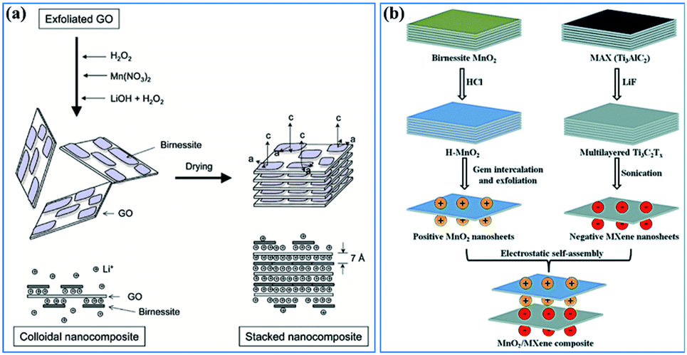 | ||
| Fig. 14 (a) Schematic representation of GO–birnessite nanocomposites.169 (b) Illustration of the process of preparing the birnessite/MXene composite.170 | ||
(iii) Enhancing the electrolyte ionic adsorbability of birnessite. Based on the energy storage mechanism of birnessite, the electrolyte ionic adsorbabilities of birnessite depend on its surface oxygen atoms. Enhancing the adsorption affinity of these oxygen atoms should be a feasible means to boost its specific capacitance. Introducing other nonmetal heteroatoms, altering the interlayer ionic species and adjusting the content of Mn4+ are some possible strategies. Particularly, a desirable birnessite single-layer slab composed of Mn4+ and all the MnO6 octahedra can be involved in electrochemical reactions, which will exhibit its theoretical capacitance (Fig. 13c).
(iv) As mentioned in the energy storage mechanism, reducing the dead mass of birnessite by adjusting the crystal orientation of birnessite can be another solution to enhance its electrochemical properties. Increasing the extent of the c axis and shortening the extent of the c axis and b axis will decrease the diffusion-controlled contribution and increase surface capacitive contribution extremely, resulting in an enhanced electrochemical performance (Fig. 13d).
In conclusion, birnessite, as a layered structure of MnO2, plays an important role in energy storage applications and energy conversion systems because of its low cost, nontoxicity and high operability. To date, birnessite based smart structures with different functions have been extensively investigated and some special architectures also can be applied as energy storage electrodes. We hope that this review can helps us construct more and more smart birnessite based structures for supercapacitors.
Conflicts of interest
There are no conflicts to declare.Acknowledgements
This work received financial support from the National Natural Science Foundation of China (Grant no. 21576034, 51908092), the Joint Funds of the National Natural Science Foundation of China-Guangdong (Grant no. U1801254), a project funded by the Chongqing Special Postdoctoral Science Foundation (XmT2018043), the Technological projects of Chongqing Municipal Education Commission (KJZDK201800801), and the Innovative Research Team of Chongqing (CXTDG201602014).References
- R. McKenzie, Mineral. Mag., 1971, 38, 493–502 CrossRef CAS.
- V. A. Drits, E. Silvester, A. I. Gorshkov and A. Manceau, Am. Mineral., 1997, 82, 946–961 CAS.
- L. Jones and A. A. Milne, Mineral. Mag. J. Mineral. Soc., 1956, 31, 283–288 CrossRef CAS.
- E. Silvester, A. Manceau and V. A. Drits, Am. Mineral., 1997, 82, 962–978 CAS.
- J. E. Post and D. R. Veblen, Am. Mineral., 1990, 75, 477–489 CAS.
- B. Lanson, V. A. Drits, A. C. Gaillot, E. Silvester, A. Plançon and A. Manceau, Am. Mineral., 2002, 87, 1631–1645 CrossRef CAS.
- S. Zhang, K. J. Livi, A. C. Gaillot, A. T. Stone and D. R. Veblen, Am. Mineral., 2010, 95, 1741–1746 CrossRef CAS.
- C. Julien, M. Massot, R. Baddour-Hadjean, S. Franger, S. Bach and J. Pereira-Ramos, Solid State Ionics, 2003, 159, 345–356 CrossRef CAS.
- D. Golden, J. Dixon and C. Chen, Clays Clay Miner., 1986, 34, 511–520 CrossRef CAS.
- Q. Feng, K. Yanagisawa and N. Yamasaki, J. Mater. Sci. Lett., 1997, 16, 110–112 CrossRef CAS.
- L. Athouël, F. Moser, R. Dugas, O. Crosnier, D. Bélanger and T. Brousse, J. Phys. Chem. C, 2008, 112, 7270–7277 CrossRef.
- S. Komaba, A. Ogata and T. Tsuchikawa, Electrochem. Commun., 2008, 10, 1435–1437 CrossRef CAS.
- H. Jiang, C. Li, T. Sun and J. Ma, Nanoscale, 2012, 4, 807–812 RSC.
- W. Wei, X. Cui, W. Chen and D. G. Ivey, Chem. Soc. Rev., 2011, 40, 1697–1721 RSC.
- Y. X. Zhang, S. Zhu, M. Dong, C. P. Liu and Z. Q. Wen, Int. J. Electrochem. Sci., 2013, 8, 2407–2416 CAS.
- Z. Zhang, C. Ma, M. Huang, F. Li, S. Zhu, C. Hua, L. Yu, H. Zheng, X. Hu and Y. Zhang, J. Mater. Sci.: Mater. Electron., 2015, 26, 4212–4220 CrossRef CAS.
- X. Fu, X. Wang, Y. Chen, W. Huo, X. Liu, K. Chen, F. Dong, H. C. Yao and Y. Zhang, J. Colloid Interface Sci., 2019, 557, 168–173 CrossRef CAS.
- M. Toupin, T. Brousse and D. Bélanger, Chem. Mater., 2004, 16, 3184–3190 CrossRef CAS.
- X. Tao, J. Du, Y. Sun, S. Zhou, Y. Xia, H. Huang, Y. Gan, W. Zhang and X. Li, Adv. Funct. Mater., 2013, 23, 4745–4751 CAS.
- D. Chen, D. Ding, X. Li, G. H. Waller, X. Xiong, M. A. El-Sayed and M. Liu, Chem. Mater., 2015, 27, 6608–6619 CrossRef CAS.
- H. Kanoh, W. Tang, Y. Makita and K. Ooi, Langmuir, 1997, 13, 6845–6849 CrossRef CAS.
- M. Kim and J. Kim, ACS Appl. Mater. Interfaces, 2014, 6, 9036–9045 CrossRef CAS.
- T. Brousse, M. Toupin, R. Dugas, L. Athouël, O. Crosnier and D. Bélanger, J. Electrochem. Soc., 2006, 153, A2171–A2180 CrossRef CAS.
- K. Makgopa, P. M. Ejikeme, C. J. Jafta, K. Raju, M. Zeiger, V. Presser and K. I. Ozoemena, J. Mater. Chem. A, 2015, 3, 3480–3490 RSC.
- Y. Zhang, S. Zhu, X. Hao, C. Liu and Z. Wen, Ceram. Int., 2014, 40, 13381–13388 CrossRef CAS.
- C. Liu, Y. Chen, Z. Dong, X. Wu, Y. Situ and H. Huang, Electrochim. Acta, 2019, 298, 678–684 CrossRef CAS.
- T. Wang, F. Dong and Y. X. Zhang, Mater. Lett., 2016, 171, 319–322 CrossRef CAS.
- P. Liu, Y. Zhu, X. Gao, Y. Huang, Y. Wang, S. Qin and Y. Zhang, Chem. Eng. J., 2018, 350, 79–88 CrossRef CAS.
- J.-G. Wang, Y. Yang, Z.-H. Huang and F. Kang, Carbon, 2013, 61, 190–199 CrossRef CAS.
- Z. Q. Wen, M. Li, S. J. Zhu and T. Wang, Int. J. Electrochem. Sci., 2016, 11, 1810–1820 CAS.
- W. Li, K. Xu, B. Li, J. Sun, F. Jiang, Z. Yu, R. Zou, Z. Chen and J. Hu, ChemElectroChem, 2014, 1, 1003–1008 CrossRef CAS.
- V. Subramanian, H. Zhu, R. Vajtai, P. Ajayan and B. Wei, J. Phys. Chem. B, 2005, 109, 20207–20214 CrossRef CAS PubMed.
- M. Huang, Y. Zhang, F. Li, L. Zhang, R. S. Ruoff, Z. Wen and Q. Liu, Sci. Rep., 2014, 4, 3878 CrossRef.
- J. Chang, M. Jin, F. Yao, T. H. Kim, V. T. Le, H. Yue, F. Gunes, B. Li, A. Ghosh and S. Xie, Adv. Funct. Mater., 2013, 23, 5074–5083 CrossRef CAS.
- S. He and W. Chen, J. Power Sources, 2015, 294, 150–158 CrossRef CAS.
- Z. Fan, J. Yan, T. Wei, L. Zhi, G. Ning, T. Li and F. Wei, Adv. Funct. Mater., 2011, 21, 2366–2375 CrossRef CAS.
- L. Yuan, X.-H. Lu, X. Xiao, T. Zhai, J. Dai, F. Zhang, B. Hu, X. Wang, L. Gong and J. Chen, ACS Nano, 2011, 6, 656–661 CrossRef PubMed.
- X. L. Guo, M. Kuang, F. Li, X. Y. Liu, Y. X. Zhang, F. Dong and D. Losic, Electrochim. Acta, 2016, 190, 159–167 CrossRef CAS.
- G. Liu, C. Kang, J. Fang, L. Fu, H. Zhou and Q. Liu, J. Power Sources, 2019, 431, 48–54 CrossRef CAS.
- H. Du, C. Wang and J. Lv, Solid State Commun., 2018, 277, 19–24 CrossRef CAS.
- J. Lv, M. Yang, T. Liang and H. Miura, Mater. Lett., 2017, 197, 127–130 CrossRef CAS.
- L. Yu, G. Q. Zhang, C. Z. Yuan and X. W. Lou, Chem. Commun., 2013, 49, 137–139 RSC.
- Z. Yu, B. Duong, D. Abbitt and J. Thomas, Adv. Mater., 2013, 25, 3302–3306 CrossRef CAS PubMed.
- I. I. Misnon and R. Jose, New J. Chem., 2017, 41, 6574–6584 RSC.
- S.-B. Yoon and K.-B. Kim, Electrochim. Acta, 2013, 106, 135–142 CrossRef CAS.
- H. Jiang, J. Ma and C. Li, J. Mater. Chem., 2012, 22, 16939–16942 RSC.
- J. Kang, A. Hirata, L. Kang, X. Zhang, Y. Hou, L. Chen, C. Li, T. Fujita, K. Akagi and M. Chen, Angew. Chem., Int. Ed., 2013, 52, 1664–1667 CrossRef CAS.
- L. Liu, M. Min, F. Liu, H. Yin, Y. Zhang and G. Qiu, J. Power Sources, 2015, 277, 26–35 CrossRef CAS.
- S. Zhu, L. Li, J. Liu, H. Wang, T. Wang, Y. Zhang, L. Zhang, R. S. Ruoff and F. Dong, ACS Nano, 2018, 12, 1033–1042 CrossRef CAS PubMed.
- N. Jabeen, A. Hussain, Q. Xia, S. Sun, J. Zhu and H. Xia, Adv. Mater., 2017, 29, 1700804 CrossRef.
- T. Xiong, T. L. Tan, L. Lu, W. S. V. Lee and J. Xue, Adv. Energy Mater., 2018, 8, 1702630 CrossRef.
- Y. Liu, D. Yan, Y. Li, Z. Wu, R. Zhuo, S. Li, J. Feng, J. Wang, P. Yan and Z. Geng, Electrochim. Acta, 2014, 117, 528–533 CrossRef CAS.
- L.-F. Chen, Z.-H. Huang, H.-W. Liang, Q. F. Guan and S. H. Yu, Adv. Mater., 2013, 25, 4746–4752 CrossRef CAS.
- X. Lu, M. Yu, G. Wang, T. Zhai, S. Xie, Y. Ling, Y. Tong and Y. Li, Adv. Mater., 2013, 25, 267–272 CrossRef CAS.
- Q. Li, Z.-L. Wang, G.-R. Li, R. Guo, L. X. Ding and Y. X. Tong, Nano Lett., 2012, 12, 3803–3807 CrossRef CAS PubMed.
- L. Bao, J. Zang and X. Li, Nano Lett., 2011, 11, 1215–1220 CrossRef CAS PubMed.
- P. Yang, Y. Ding, Z. Lin, Z. Chen, Y. Li, P. Qiang, M. Ebrahimi, W. Mai, C. P. Wong and Z. L. Wang, Nano Lett., 2014, 14, 731–736 CrossRef CAS PubMed.
- Y. He, W. Chen, X. Li, Z. Zhang, J. Fu, C. Zhao and E. Xie, ACS Nano, 2013, 7, 174–182 CrossRef CAS.
- J. Ge, H.-B. Yao, W. Hu, X. F. Yu, Y. X. Yan, L. B. Mao, H.-H. Li, S.-S. Li and S.-H. Yu, Nano Energy, 2013, 2, 505–513 CrossRef CAS.
- Z. Zhang, F. Xiao, L. Qian, J. Xiao, S. Wang and Y. Liu, Adv. Energy Mater., 2014, 4, 1400064 CrossRef.
- G. Yu, L. Hu, N. Liu, H. Wang, M. Vosgueritchian, Y. Yang, Y. Cui and Z. Bao, Nano Lett., 2011, 11, 4438–4442 CrossRef CAS PubMed.
- S. Ching, D. J. Petrovay, M. L. Jorgensen and S. L. Suib, Inorg. Chem., 1997, 36, 883–890 CrossRef CAS.
- B. M. Tebo, J. R. Bargar, B. G. Clement, G. J. Dick, K. J. Murray, D. Parker, R. Verity and S. M. Webb, Annu. Rev. Earth Planet. Sci., 2004, 32, 287–328 CrossRef CAS.
- Q. Feng, H. Kanoh and K. Ooi, J. Mater. Chem., 1999, 9, 319–333 RSC.
- X. Zhang, P. Yu, H. Zhang, D. Zhang, X. Sun and Y. Ma, Electrochim. Acta, 2013, 89, 523–529 CrossRef CAS.
- W. Xiao, D. L. Wang and X. W. Lou, J. Phys. Chem. C, 2010, 114, 1694–1700 CrossRef CAS.
- S. Zhu, W. Cen, L. Hao, J. Ma, L. Yu, H. Zheng and Y. Zhang, Mater. Lett., 2014, 135, 11–14 CrossRef CAS.
- M. Huang, R. Mi, H. Liu, F. Li, X. L. Zhao, W. Zhang, S. X. He and Y. X. Zhang, J. Power Sources, 2014, 269, 760–767 CrossRef CAS.
- Z. Hu, X. Xiao, C. Chen, T. Li, L. Huang, C. Zhang, J. Su, L. Miao, J. Jiang, Y. Zhang and J. Zhou, Nano Energy, 2015, 11, 226–234 CrossRef CAS.
- G. Wang, L. Zhang and J. Zhang, Chem. Soc. Rev., 2012, 41, 797–828 RSC.
- S. Zhu, T. Wang, X. Liu, Y. Zhang, F. Li, F. Dong, H. Zhang and L. Zhang, ACS Appl. Energy Mater., 2018, 2, 1051–1059 CrossRef.
- J. Liu, C. Xu, Z. Chen, S. Ni and Z. X. Shen, Green Energy & Environment, 2018, 3, 20–41 Search PubMed.
- L. L. Zhang and X. S. Zhao, Chem. Soc. Rev., 2009, 38, 2520–2531 RSC.
- T. Brousse, D. Belanger and J. W. Long, J. Electrochem. Soc., 2015, 162, A5185–A5189 CrossRef CAS.
- W. Gu, M. Sevilla, A. Magasinski, A. B. Fuertes and G. Yushin, Energy Environ. Sci., 2013, 6, 2465–2476 RSC.
- H. Jiang, P. S. Lee and C. Li, Energy Environ. Sci., 2013, 6, 41–53 RSC.
- Y. Zhang and D. Xue, Energy Environ. Focus, 2012, 1, 4–18 CrossRef.
- R. Tholkappiyan, A. N. Naveen, K. Vishista and F. Hamed, J. Taibah Univ. Sci., 2018, 12, 669–677 CrossRef.
- T. Qin, S. Dang, J. Hao, Z. Wang, H. Li, Y. Wen, S. Lu, D. He, G. Cao and S. Peng, Dalton Trans., 2018, 47, 11503–11511 RSC.
- X. Liao, Y. Zhao, J. Wang, W. Yang, L. Xu, X. Tian, Y. Shuang, K. A. Owusu, M. Yan and L. Mai, Nano Res., 2018, 11, 2083–2092 CrossRef CAS.
- Z. Sun, Y. Zhang, Y. Liu, J. Fu, S. Cheng, P. Cui and E. Xie, J. Power Sources, 2019, 436, 226795 CrossRef CAS.
- X. Zhang, Q. Fu, H. Huang, L. Wei and X. Guo, Small, 2019, 15, 1805235 CrossRef PubMed.
- M. Yao, X. Ji, T.-F. Chou, S. Cheng, L. Yang, P. Wu, H. Luo, Y. Zhu, L. Tang, J. Wang and M. Liu, ACS Appl. Energy Mater., 2019, 2, 2743–2750 CrossRef CAS.
- Z. Ma, F. Jing, Y. Fan, L. Hou, L. Su, L. Fan and G. Shao, Small, 2019, 15, 1900862 CrossRef PubMed.
- T. C. Liu, W. G. Pell, B. E. Conway and S. L. Roberson, J. Electrochem. Soc., 1998, 145, 1882–1888 CrossRef CAS.
- J. Wang, J. Polleux, J. Lim and B. Dunn, J. Phys. Chem. C, 2007, 111, 14925–14931 CrossRef CAS.
- X. Guo, T. Wang, T. X. Zheng, C. Xu, J. Zhang, Y. X. Zhang, X. Y. Liu and F. Dong, J. Mater. Chem. A, 2018, 6, 24717–24727 RSC.
- M. Sathiya, A. S. Prakash, K. Ramesha, J. M. Tarascon and A. K. Shukla, J. Am. Chem. Soc., 2011, 133, 16291–16299 CrossRef CAS PubMed.
- N. Jabeen, Q. Xia, S. V. Savilov, S. M. Aldoshin, Y. Yu and H. Xia, ACS Appl. Mater. Interfaces, 2016, 8, 33732–33740 CrossRef CAS PubMed.
- W. Guo, C. Yu, S. Li, Z. Wang, J. Yu, H. Huang and J. Qiu, Nano Energy, 2019, 57, 459–472 CrossRef CAS.
- J. Hao, Y. Zhong, Y. Liao, D. Shu, Z. Kang, X. Zou, C. He and S. Guo, Electrochim. Acta, 2015, 167, 412–420 CrossRef CAS.
- C. Xiong, T. Li, M. Khan, H. Li and T. Zhao, RSC Adv., 2015, 5, 85613–85619 RSC.
- Y. Liu, X. Miao, J. Fang, X. Zhang, S. Chen, W. Li, W. Feng, Y. Chen, W. Wang and Y. Zhang, ACS Appl. Mater. Interfaces, 2016, 8, 5251–5260 CrossRef CAS PubMed.
- Y. Liu, X. Cai, B. Luo, M. Yan, J. Jiang and W. Shi, Carbon, 2016, 107, 426–432 CrossRef CAS.
- Y. Song, Z. Li, K. Guo and T. Shao, Nanoscale, 2016, 8, 15671–15680 RSC.
- F. Ochai-Ejeh, M. J. Madito, K. Makgopa, M. N. Rantho, O. Olaniyan and N. Manyala, Electrochim. Acta, 2018, 289, 363–375 CrossRef CAS.
- K. Zhang, H. Zhao, Z. Zhang, J. Chen, X. Mu, X. Pan, Z. Zhang, J. Zhou, J. Li and E. Xie, Carbon, 2015, 95, 746–755 CrossRef CAS.
- G. Huang, Y. Zhang, L. Wang, P. Sheng and H. Peng, Carbon, 2017, 125, 595–604 CrossRef CAS.
- M. Hu, C. Cui, C. Shi, Z.-S. Wu, J. Yang, R. Cheng, T. Guang, H. Wang, H. Lu and X. Wang, ACS Nano, 2019, 13, 6899–6905 CrossRef CAS PubMed.
- J. Zhou, H. Zhao, X. Mu, J. Chen, P. Zhang, Y. Wang, Y. He, Z. Zhang, X. Pan and E. Xie, Nanoscale, 2015, 7, 14697–14706 RSC.
- D. Gueon and J. H. Moon, ACS Sustainable Chem. Eng., 2017, 5, 2445–2453 CrossRef CAS.
- M. Kim, Y. Hwang, K. Min and J. Kim, Electrochim. Acta, 2013, 113, 322–331 CrossRef CAS.
- M. Nakayama, S. Osae, K. Kaneshige, K. Komine and H. Abe, J. Electrochem. Soc., 2016, 163, A2340–A2348 CrossRef CAS.
- T. Liu, Z. Zhou, Y. Guo, D. Guo and G. Liu, Nat. Commun., 2019, 10, 675 CrossRef PubMed.
- M. D. Stoller, S. Park, Y. Zhu, J. An and R. S. Ruoff, Nano Lett., 2008, 8, 3498–3502 CrossRef CAS PubMed.
- L. Peng, X. Peng, B. Liu, C. Wu, Y. Xie and G. Yu, Nano Lett., 2013, 13, 2151–2157 CrossRef CAS PubMed.
- P. Wu, S. Cheng, L. Yang, Z. Lin, X. Gui, X. Ou, J. Zhou, M. Yao, M. Wang, Y. Zhu and M. Liu, ACS Appl. Mater. Interfaces, 2016, 8, 23721–23728 CrossRef CAS PubMed.
- T. Qiu, B. Luo, M. Giersig, E. M. Akinoglu, L. Hao, X. Wang, L. Shi, M. Jin and L. Zhi, Small, 2014, 10, 4136–4141 CAS.
- S. Zhu, Q. Shan, F. Dong, Y. Zhang and L. Zhang, Gold Bull., 2017, 50, 61–68 CrossRef CAS.
- X. Peng, Y. Guo, Q. Yin, J. Wu, J. Zhao, C. Wang, S. Tao, W. Chu, C. Wu and Y. Xie, J. Am. Chem. Soc., 2017, 139, 5242–5248 CrossRef CAS PubMed.
- C. Zener, Phys. Rev., 1951, 82, 403–405 CrossRef CAS.
- G. Wang, Z. Ma, G. Zhang, C. Li and G. Shao, Electrochim. Acta, 2015, 182, 1070–1077 CrossRef CAS.
- G. Wang, G. Shao, J. Du, Y. Zhang and Z. Ma, Mater. Chem. Phys., 2013, 138, 108–113 CrossRef CAS.
- H. Liu, W. Gu, B. Luo, P. Fan, L. Liao, E. Tian, Y. Niu, J. Fu, Z. Wang, Y. Wu, G. Lv and L. Mei, Electrochim. Acta, 2018, 291, 31–40 CrossRef CAS.
- H. Peng, H. Fan, M. Zhang and L. Ning, Appl. Phys. A: Mater. Sci. Process., 2018, 124, 482 CrossRef.
- Q. Peng, L. Liu, Y. Luo, Y. Zhang, W. Tan, F. Liu, S. L. Suib and G. Qiu, ACS Appl. Mater. Interfaces, 2016, 8, 34405–34413 CrossRef CAS PubMed.
- R. Dong, Q. Ye, L. Kuang, X. Lu, Y. Zhang, X. Zhang, G. Tan, Y. Wen and F. Wang, ACS Appl. Mater. Interfaces, 2013, 5, 9508–9516 CrossRef CAS PubMed.
- X. Su, L. Yu, G. Cheng, H. Zhang, M. Sun, L. Zhang and J. Zhang, Appl. Energy, 2014, 134, 439–445 CrossRef CAS.
- H. Z. Chi, Y. Li, Y. Xin and H. Qin, Chem. Commun., 2014, 50, 13349–13352 RSC.
- S. Zhao, T. Liu, D. Hou, W. Zeng, B. Miao, S. Hussain, X. Peng and M. S. Javed, Appl. Surf. Sci., 2015, 356, 259–265 CrossRef CAS.
- B. Ming, J. Li, F. Kang, G. Pang, Y. Zhang, L. Chen, J. Xu and X. Wang, J. Power Sources, 2012, 198, 428–431 CrossRef CAS.
- D. Yan, H. Zhang, S. Li, G. Zhu, Z. Wang, H. Xu and A. Yu, J. Alloys Compd., 2014, 607, 245–250 CrossRef CAS.
- A. Boisset, L. Athouel, J. Jacquemin, P. Porion, T. Brousse and M. Anouti, J. Phys. Chem. C, 2013, 117, 7408–7422 CrossRef CAS.
- Z. Li, J. Wang, Z. Wang, H. Ran, Y. Li, X. Han and S. Yang, New J. Chem., 2012, 36, 1490–1495 RSC.
- S. J. Zhu, J. Zhang, J. J. Ma, Y. X. Zhang and K. X. Yao, J. Power Sources, 2015, 278, 555–561 CrossRef CAS.
- F. Li, Y. X. Zhang, M. Huang, Y. Xing and L. L. Zhang, Electrochim. Acta, 2015, 154, 329–337 CrossRef CAS.
- M. Shen, S. J. Zhu, X. Liu, X. Fu, W. C. Huo, X. L. Liu, Y. X. Chen, Q. Y. Shan, H.-C. Yao and Y. X. Zhang, CrystEngComm, 2019, 21, 5322–5331 RSC.
- H. Z. Chi, S. Yin, H. Qin and K. Su, Mater. Lett., 2016, 162, 131–134 CrossRef.
- C. Chai, A. Liu, Y. Wang, Y. Lu and H. Che, Ceram. Int., 2018, 44, 16923–16930 CrossRef CAS.
- W. Xiao, W. Zhou, H. Yu, Y. Pu, Y. Zhang and C. Hu, Electrochim. Acta, 2018, 264, 1–11 CrossRef CAS.
- L. Gao, L. Zhang, S. Jia, X. Liu, Y. Wang and S. Xing, Electrochim. Acta, 2016, 203, 59–65 CrossRef CAS.
- Y. Zhang, M. Dong, S. Zhu, C. Liu and Z. Wen, Mater. Res. Bull., 2014, 49, 448–453 CrossRef CAS.
- Y. Munaiah, B. G. S. Raj, T. P. Kumar and P. Ragupathy, J. Mater. Chem. A, 2013, 1, 4300–4306 RSC.
- Z. Q. Wen, M. Li, F. Li, S. J. Zhu, X. Y. Liu, Y. X. Zhang, T. Kumeria, D. Losic, Y. Gao, W. Zhang and S. X. He, Dalton Trans., 2016, 45, 936–942 RSC.
- Q. J. Le, T. Wang, D. N. H. Tran, F. Dong, Y. X. Zhang and D. Losic, J. Mater. Chem. A, 2017, 5, 10856–10865 RSC.
- Y. Zhang, W. W. Guo, T. X. Zheng, Y. X. Zhang and X. Fan, Appl. Surf. Sci., 2018, 427, 1158–1165 CrossRef CAS.
- A. L. M. Reddy, M. M. Shaijumon, S. R. Gowda and P. M. Ajayan, J. Phys. Chem. C, 2010, 114, 658–663 CrossRef CAS.
- B. Patil, S. Ahn, S. Yu, H. Song, Y. Jeong, J. H. Kim and H. Ahn, Carbon, 2018, 134, 366–375 CrossRef CAS.
- G.-X. Li, P.-X. Hou, J. Luan, J.-C. Li, X. Li, H. Wang, C. Shi, C. Liu and H.-M. Cheng, Carbon, 2018, 140, 634–643 CrossRef CAS.
- Q. Wang, Y. Ma, X. Liang, D. Zhang and M. Miao, Chem. Eng. J., 2019, 371, 145–153 CrossRef CAS.
- F. Cheng, T. Zhang, Y. Zhang, J. Du, X. Han and J. Chen, Angew. Chem., Int. Ed., 2013, 52, 2474–2477 CrossRef CAS.
- M. K. Song, S. Cheng, H. Chen, W. Qin, K.-W. Nam, S. Xu, X.-Q. Yang, A. Bongiorno, J. Lee, J. Bai, T. A. Tyson, J. Cho and M. Liu, Nano Lett., 2012, 12, 3483–3490 CrossRef CAS.
- T. Zhai, X. Lu, F. Wang, H. Xia and Y. Tong, Nanoscale Horiz., 2016, 1, 109–124 RSC.
- Y. Huang, Y. Li, Z. Hu, G. Wei, J. Guo and J. Liu, J. Mater. Chem. A, 2013, 1, 9809–9813 RSC.
- P. Gao, P. Metz, T. Hey, Y. Gong, D. Liu, D. D. Edwards, J. Y. Howe, R. Huang and S. T. Misture, Nat. Commun., 2017, 8, 14559 CrossRef CAS.
- Y. Wang, Y. Lu, K. Chen, S. Cui, W. Chen and L. Mi, Electrochim. Acta, 2018, 283, 1087–1094 CrossRef CAS.
- W. He, C. Wang, F. Zhuge, X. Deng, X. Xu and T. Zhai, Nano Energy, 2017, 35, 242–250 CrossRef CAS.
- G. Nie, X. Lu, M. Chi, Y. Zhu, Z. Yang, N. Song and C. Wang, Electrochim. Acta, 2017, 231, 36–43 CrossRef CAS.
- Z. Ma, G. Shao, Y. Fan, G. Wang, J. Song and D. Shen, ACS Appl. Mater. Interfaces, 2016, 8, 9050–9058 CrossRef CAS PubMed.
- H. Y. Wang, F. X. Xiao, L. Yu, B. Liu and X. W. Lou, Small, 2014, 10, 3181–3186 CrossRef CAS.
- Y. Guo, L. Yu, C. Y. Wang, Z. Lin and X. W. Lou, Adv. Funct. Mater., 2015, 25, 5184–5189 CrossRef CAS.
- Y. Guo, C. Wu, N.-W. Li, S. Yuan and L. Yu, J. Mater. Chem. A, 2019 10.1039/c9ta05790k.
- W. Xiao, J. S. Chen and X. W. Lou, CrystEngComm, 2011, 13, 5685–5687 RSC.
- S. J. Zhu, J. Q. Jia, T. Wang, D. Zhao, J. Yang, F. Dong, Z. G. Shang and Y. X. Zhang, Chem. Commun., 2015, 51, 14840–14843 RSC.
- J. Liu, J. Jiang, C. Cheng, H. Li, J. Zhang, H. Gong and H. J. Fan, Adv. Mater., 2011, 23, 2076 CrossRef CAS.
- M. Huang, Y. Zhang, F. Li, Z. Wang, Alamusi, N. Hu, Z. Wen and Q. Liu, Sci. Rep., 2014, 4, 4518 CrossRef.
- J. Liu, J. Jiang, M. Bosman and H. J. Fan, J. Mater. Chem., 2012, 22, 2419–2426 RSC.
- H. Jiang, C. Li, T. Sun and J. Ma, Chem. Commun., 2012, 48, 2606–2608 RSC.
- M. U. A. Prathap, V. Anuraj, B. Satpati and R. Srivastava, J. Hazard. Mater., 2013, 262, 766–774 CrossRef.
- M. Kundu, G. Singh and A. M. Svensson, New J. Chem., 2019, 43, 1257–1266 RSC.
- Z. Wang, F. Wang, J. Tu, D. Cao, X. An and Y. Ye, Mater. Lett., 2016, 171, 10–13 CrossRef CAS.
- H. Chen, X. L. Liu, J. M. Zhang, F. Dong and Y. X. Zhang, Ceram. Int., 2016, 42, 8909–8914 CrossRef CAS.
- R. J. Ramalingam, N. Konikkara, H. Al-Lohedan, D. M. Al-dhayan, L. J. Kennedy, S. K. K. Basha and S. R. M. Sayed, Int. J. Hydrogen Energy, 2018, 43, 17121–17131 CrossRef.
- X. Hao, Y. Zhang, Z. Diao, H. Chen, A. Zhang and Z. Wang, RSC Adv., 2014, 4, 63901–63908 RSC.
- W. Quan, C. Jiang, S. Wang, Y. Li, Z. Zhang, Z. Tang and F. Favier, Electrochim. Acta, 2017, 247, 1072–1079 CrossRef CAS.
- W. Zheng, S. Sun, Y. Xu, R. Yu and H. Li, J. Alloys Compd., 2018, 768, 240–248 CrossRef CAS.
- D. Kong, J. Luo, Y. Wang, W. Ren, T. Yu, Y. Luo, Y. Yang and C. Cheng, Adv. Funct. Mater., 2014, 24, 3815–3826 CrossRef CAS.
- Z. Liu, K. Xu, H. Sun and S. Yin, Small, 2015, 11, 2182–2191 CrossRef CAS.
- X. J. Yang, Y. Makita, Z. H. Liu and K. Ooi, Chem. Mater., 2003, 15, 1228–1231 CrossRef CAS.
- S. Chen, Y. Xiang, W. Xu and C. Peng, Inorg. Chem. Front., 2019, 6, 199–208 RSC.
Footnote |
| † These authors contributed equally to this work. |
| This journal is © The Royal Society of Chemistry 2020 |