
 Open Access Article
 This Open Access Article is licensed under a Creative Commons Attribution-Non Commercial 3.0 Unported Licence
Rectifying behavior in twisted bilayer black phosphorus nanojunctions mediated through intrinsic anisotropy†
Vivekanand
Shukla
 *a,
Anton
Grigoriev
*a and
Rajeev
Ahuja
ab
*a,
Anton
Grigoriev
*a and
Rajeev
Ahuja
ab
aCondensed Matter Theory Group, Materials Theory Division, Department of Physics and Astronomy, Uppsala University, Box 516, SE-75120, Uppsala, Sweden. E-mail: Vivekanand.Shukla@physics.uu.se; Anton.Grogoriev@physics.uu.se
bApplied Materials Physics, Department of Materials and Engineering, Royal Institute of Technology (KTH), SE-10044, Stockholm, Sweden
First published on 12th February 2020
Abstract
We explore the possibility of using van der Waals bonded heterostructures of stacked together 2D bilayer black phosphorus (BP) for nanoscale device applications. The electronic properties of BP in AA stacking and 90° twisted are studied with density functional theory. Furthermore, we study the homogeneous nanojunction architecture of BP to use its anisotropic properties. Using the first principles simulations along with the NEGF approach, we calculate the quantum transport properties of the nanojunction setup. The interlayer direction dependent current characteristics are explained in different setups. Our result revealed that the 90° twisted nanojunction device would be a potential rectifier despite having no p–n junction characteristics only due to the intrinsic anisotropy of the material, making tunneling between armchair- and zigzag-directional BP sheets asymmetric.
Introduction
Modern nanodevices explore either the quantum properties of nanosized (e.g. two dimensional, 2D) materials or the properties that arise at nanosized features like defects or interfaces. Geim and Grigorieva introduced1 the concept that explores both approaches simultaneously, by looking at vertical vs. lateral junctions. However, in practical applications, most of the 2D hetero and homo junctions are neither purely vertical nor completely lateral as is often assumed in theory.2,3 In this paper we would like to propose a simple method to build a nanodevice from 2D nanomaterials, taking a step further and using the vertical nanojunction at the overlap of two 2D sheets of material as a lateral junction between these sheets.Let us first introduce the advantages of our building blocks: 2D materials unveil a wide range of new physical phenomena, which would be elusive in their bulk counterparts, and mass-less Dirac fermions in graphene are a good example.4–6 Apart from the fundamental interest in 2D materials, intensive research is conducted towards their real world applications, like electrochemical use, energy storage and so on.7–10 One of the important areas is electronic devices, where significant exertion is being devoted to integrating 2D materials into nano- and micro-electronic devices in the forms other than monolayers.11,12 The synthesis of new materials by stacking monolayers of the same or two different materials, t.ex. the epitaxial growth of superlattices, has been a subject of fervent research for decades.13 The concept of van der Waals (vdW) heterostructures was conceptualized by Geim and Grigorieva a few years back.1 These vdW heterostructures are materialized by stacking of two 2D crystalline atomic layers, with no chemical bond between them.14,15 The stacking patterns unfold the world of possibilities of any desired heterostructure with specified chemical/physical and electronic properties. These heterostructures have been studied widely both theoretically and experimentally like graphene/hexagonal boron nitride (G/h-BN), MoS2/G, MoS2/WSe2 for band alignment and charge transfer which makes them suitable for optoelectronic applications.16–18 A WSe2/h-BN/G heterostructure19 was reported for programmable p–n junction diodes and the same property has also been recited for TMD/G, h-BN/TMD, G/BN and TMD/TMD and several others.20–24
There are lateral nanodevices, where the interface between two 2D sheets takes the form of the monolayer–bilayer–monolayer junction (ML–BL–ML) structure. For electronic nanodevices one can envision a 2D monolayer (ML) at each side overlaying a metal electrode for electrical contact. We do not discuss the case where the bilayer (BL) interface is in direct contact with metal electrodes that will be sensitive to the area of the contact. Ponomarev et al. has reported WSe2/MoSe2 and WSe2/MoS2 nanojunctions in the form of ML–BL–ML for diode applications in experiment.25 Graphene and carbon nanotubes (CNTs) have also been reported in this ML–BL–ML form for negative differential resistance behavior26,27 in theoretical work.
Taking the above problem as an motivation, in this work, we performed density functional theory (DFT) with non-equilibrium Green's function (NEGF) calculations to model the bilayer structures and ML–BL–ML form of the nanojunction setup of black phosphorus (BP) or phosphorene. Recent successful exfoliation of a new class of two-dimensional materials, layered BP, has drawn both theoretical and experimental attention owing to its conspicuous electronic properties and high charge carrier mobilities of the resulting layered material.28–30 Monolayer BP has extremely high hole mobility (1000 cm2 V−1 S−1) and an on/off ratio of 104,28,30 which compares better to MoS2.31 The application of strain and electric field is helpful in tuning the electronic properties of BP.32–35 BP has also been investigated in the heterostructure form, and a graphene–BP (G–BP) heterostructure has been reported for the Schottky barrier tuning with the application of electrostatic gating.15 BP–TMCs36,37 and blue phosphorus/black phosphorus heterostructures38 are also reported for the tunable electronic properties. For the homogeneous device, few layers of BP are predicted to have good tunability and richer electronic properties compared to a monolayer, such as layer dependent band gaps and carrier mobility.39–41 The predicted layer dependent bandgap of few layer BP has been confirmed experimentally by Das et al., evidenced by layer dependent transport.42 Theoretically the bilayer BP has been reported in different stacking styles like AA, AB, AC and Aδ.40,43 Its bandgap highly depends upon these stackings. However, there are also possibilities of stacking two layers of BP at 90° which gives rise to the isotropic properties in terms of carrier transport and electronic structures. This twisted bilayer has already been reported for tunable anisotropy with electrostatic field and strain effect.44–46 Experimentally, BP mono- or few-layer form with controlled vertical gate voltage was used in device configuration as reported by Ameen et al.47
In our proposed ML–BL–ML BP nanodevice, instead of gate voltage and corresponding vertical electric field, a similar rectifying effect will be achieved by feeding the electrons from differently oriented BP monolayers into the BL junction. We started with an AA stacked BP bilayer and compared it with a 90° twisted bilayer in a 5 × 7 supercell. After gaining insight of the structural and electronic properties of these bilayers, we focused our study on the ML–BL–ML architecture of nanodevices. Using the NEGF along with the Landauer formula, we calculated the transmission function and studied I–V characteristics of the devices. We report the rectifying behavior in twisted bilayer devices achieved by using vertical tunneling between two BP sheets as a lateral interface.
Results and discussion
As the first step to use BP bilayers in the nano-junction device architecture, we simulated AA stacked bilayers and studied their electronic and structural properties. We simulated different stackings of the bilayer BP like AA, AB, and AC. Generally, the AB stacking is natural stacking with the highest possibility to form, but in our work, we consider AA stacking for further use to facilitate comparison with the twisted bilayer structure. The calculated lattice parameter for AA stacking is 4.5 Å and 3.4 Å in the armchair and zigzag direction which clearly relates to previously reported results.40 All these stacking patterns show the direct band gap properties. These stackings can also tune optical properties dramatically which has been reported in ref. 40. The AA-stacked bilayer structure is shown in Fig. 1(a) where, the interlayer distance is calculated to be 3.3 Å. Fig. 1(b) shows the band structure of AA-stacked bilayer BP, which demonstrates that the anisotropy exists in the armchair and zigzag directions and the calculated bandgap is 0.37 eV. This anisotropy and its effect on electron and hole mobility can be found elsewhere.33,39 In the band structure picture, we see no degeneracy in the conduction band minimum (CBM) and valence band maximum (VBM). This is due to strong interlayer interaction of the two extra lone pair electrons in interlayer phosphorus atoms. Furthermore, this strong layered coupling is also responsible for lowering the band gap in few-layer BP than the monolayer (reported in the ESI†). In the bilayer form, BP has the direct band gap properties which make bilayer BP an attractive material for the electronic application. Similar behaviours are found for AB and AC stackings. The bilayer structure in AB stacking is shifted by half of the cell along either the direction to get the AA stacking whereas for the AC stacking cell, one layer has to be shifted by half in both the armchair and zigzag directions to retain the AA stacked bilayer. These two differently stacked bilayers also show direct band gaps of 0.42 eV and 0.20 eV for AB and AC stacked form in GGA–PBE calculations, and anisotropic behaviour in the electronic structure and the detailed explanations can be found some somewhere in the literature. Apart from these stacking schemes the other bilayer form Aδ is reported by Lei et al.,43 which is metastable in nature. Aδ can be obtained by the shifting of the second layer along the armchair direction by 0.281a. Furthermore, the Aδ bilayer shows indirect bandgap behavior different from the rest of the above mentioned bilayers.43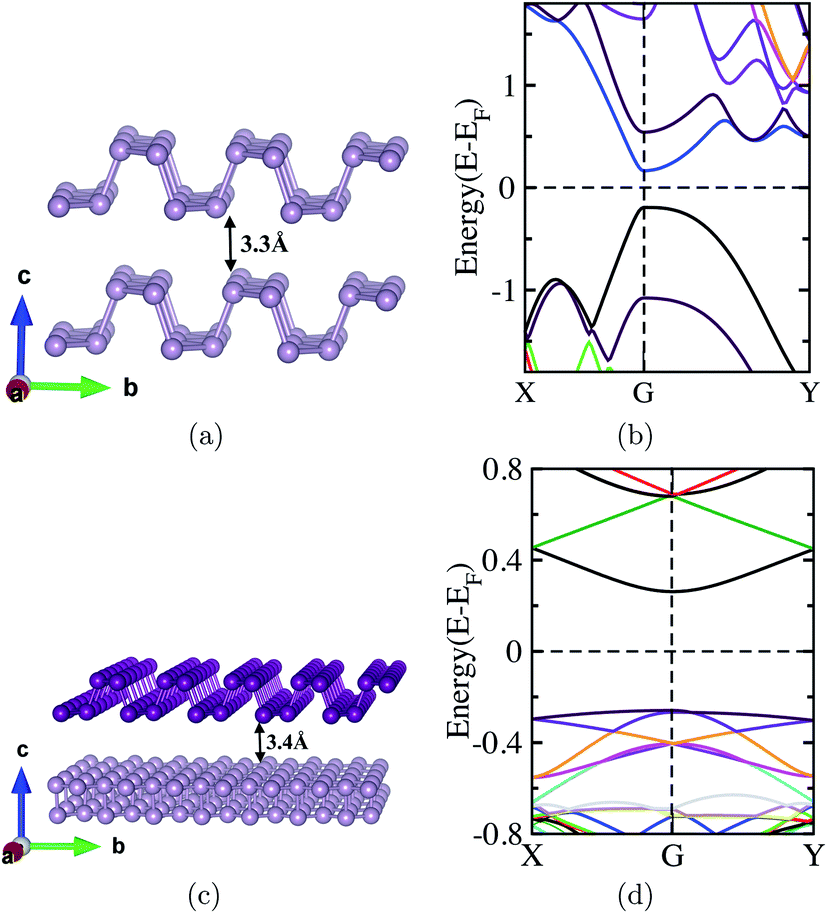 | ||
| Fig. 1 (a) Schematic picture of the AA stacked bilayer (b) band structure for the bilayer (c) 90° twisted stacked bilayer structure (upper layer is twisted by 90° to the lower layer) (d) band structure for the twisted stacked bilayer (Brillouin zone for the twisted bilayer is square). | ||
Along with the symmetric stacking scheme of bilayer BP, there is also the possibility to twist the bilayer by some rotational angles, which creates the Moire pattern.48 Here we twisted the upper layer by 90°, which in some sense makes the system laterally symmetric in structure. Fig. 1(c) shows the twisted bilayer structure, where the zigzag direction in the upper layer is the same as the armchair direction in the lower layer. A supercell approach has been used by taking the lateral dimension as 5 × 7 times that of the unit cell to minimize the lattice mismatch less than 1%. In this supercell, the two bilayers (one in the supercell and its replication) are at a distance of 30 Å, which was selected to exclude the interaction in the vertical direction from consideration. The calculated lattice parameter for this twisted bilayer unit cell is of 23.09 Å and 23.00 Å and the interlayer spacing in this fully relaxed 90° twisted bilayer cell is calculated to be 3.4 Å, which is 0.1 Å higher than that of the AA-stacked bilayer. We used vdW-DF correction for the bilayer unit cell and supercell calculations.49,50 Full relaxation of the cell volume along with the atomic positions was conducted. The P–P bond in the twisted bilayer shows only the subtle changes in comparison to naturally AA-stacked bilayers in the previous sections.
Reciprocal space geometry for the twisted bilayer would be square in the Brillouin zone. In contrast to the AA-stacked bilayer, the 90° twisted bilayer has an x–y isotropic electronic structure, means that the energy bands around X–G and G–Y are symmetric as shown in Fig. 1(d). The calculated band gap for the twisted bilayer is 0.48 eV, which is bigger than that of the AA-stacked bilayer. This clearly corresponds to the lower interaction in between the layers, which is also supported by increased interlayer spacing. The CBM is found to be singly degenerate whereas the VBM is found to be doubly degenerate by a value of 0.01 eV. Degeneracy in the VBM advocates the lack of significant hybridization near the VBM whereas CBM states are strongly coupled. These degenerate states are separated either localized in the top layer or localized in the bottom layer. More than that, this degeneracy paves the isotropy in the system where the valence band in X–G is defined by the upper layer and G–Y is defined by the bottom layer. This degeneracy and its dependence on the vertical electric field and external strain have been explained in previous reports. Band gaps in our calculations are smaller than the previously reported value by Cao et al.,45 due to the choice of functional. The vertical electric field in this twisted bilayer can induce the anisotropy in the system that can control the transport properties of this bilayer in the device form. The vertical electric field tunes the anisotropy in either direction of bands, if electric field is applied from top then the G–X band will get tuned and when it is applied from down then the G–Y band can get tuned (ESI†). External strain also leads to the effective anisotropy in the system reported by Xie et al.46 Furthermore, Fig. S1† shows the projected density of states (pDOS) plot for this twisted bilayer. The projected density in the respective layer illustrates that they do not differ with each other, which clearly demonstrates that there is no charge transfer in between the layers unlike the heterostructure made from two different materials, for example, G/BP, G/MoS2, G/h-BN, MoS2–BP and even in black phosphorus–blue phosphorus. This is a homogeneous bilayer and only symmetric twisting does not give rise to the charge transfer process.
After having a look at the electronic and structural properties of the two different bilayers we introduce the homogeneous nanojunction. Here the two layers of BP in the form of AA stacking were put on each other and then in either directions, dangling bonds were passivated by hydrogen atoms. It gives the ML–BL–ML architecture, where the central part has a bilayer of the armchair in Fig. 2(a) and zigzag in Fig. 2(b). Monolayers in these ML–BL–ML junctions are armchair and zigzag form, respectively. In our case, we deliberately created this junction to understand the difference of direction dependence in this kind of nanojunction of BP. In these two cases, a potential well is formed in this scattering region (bilayer region) shown in zigzag and armchair directions in Fig. 2(a and b), respectively. The similarity between these two nanojunctions is that the electron has to pass through the vertically stacked area through interlayer tunneling. Transport properties would be estimated from nearly the same length of the scattering region in these two devices.
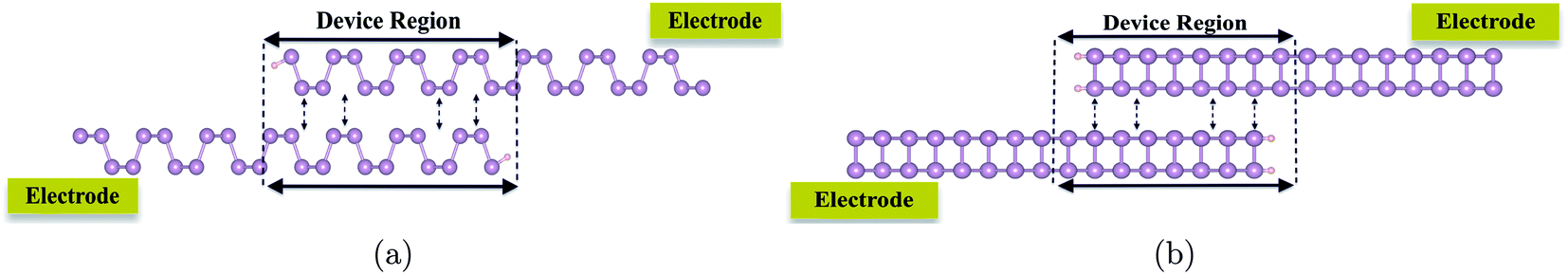 | ||
| Fig. 2 Schematic pictures for the ML–BL–ML (junction area has bilayers) nanojunction device set in (a) armchair direction and (b) zigzag direction. | ||
We would first investigate the armchair direction and further will take the consideration of the zigzag one. Zero bias transmission in the armchair nanojunction is shown in Fig. 4(b), where it shows a transmission gap of 0.9 eV. This gap resembles the monolayer electrodes with a bandgap of 0.9 eV, as the electrons are injected through the monolayer of BP and the bilayer (nanojunction) region behaves like the scattering owing to the broken periodicity. This scattering center is like a quantum well where electrons can resonate and then pass through the tunneling mechanism.
To understand the interaction between the layers in the bilayer nanojunction region and its influence upon the current–voltage (I–V) characteristics, we increased the bias in the periodic order of 0.1 V per step and calculated the current using the Landauer formula. Initially the current remains nearly zero due to the gap band gap in the monolayer electrode. Once it overcomes the energy gap of the electrodes it gives the symmetric I–V characteristics for both the positive and negative biases in Fig. 3(a). This symmetric current is due to the symmetric junction for both the positive and negative bias. Furthermore, to understand the symmetric current we can see the inset in Fig. 3(a), where transmission for both positive and negative bias at 1.8 V bias is symmetric. We see Fano resonance behavior in the transmission at the 0 eV level at 1.8 V bias; this resonance arises from the tunneling through the edges of the nanojunction. We also tried to decrease the junction area, and this eliminates the Fano resonance behavior while the overall current behavior does not change.
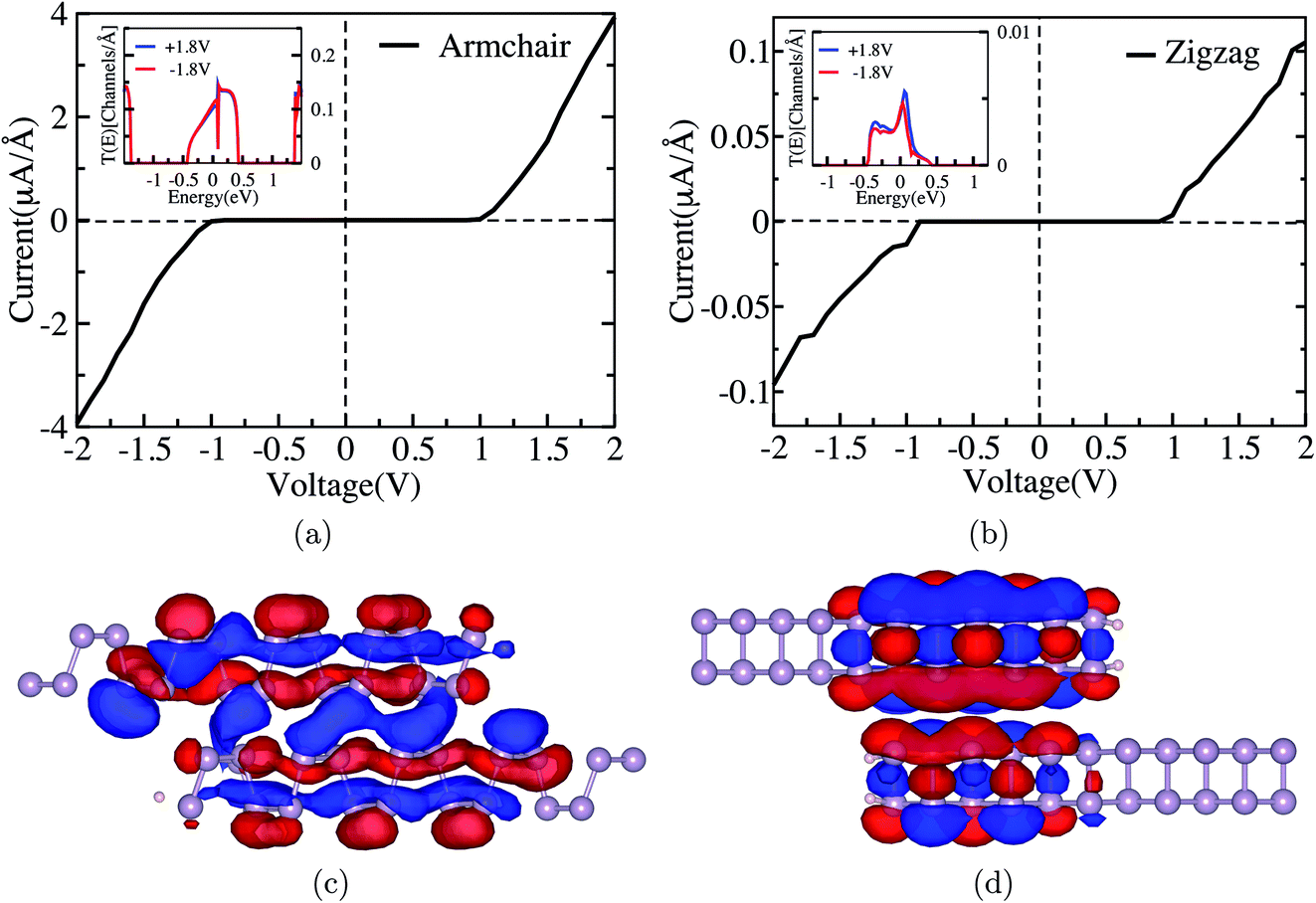 | ||
| Fig. 3 Current–voltage characteristics for symmetric nanojunction (a) armchair (b) zigzag direction (insets show the transmission function at ±1.8 V bias in the respective device) and eigenchannels for rotated bilayer nanojunctions at +1.8 V at the Fermi level (c) armchair direction and (d) zigzag direction. | ||
We now consider the case on the zigzag direction which has lower transmission than that of the armchair direction at zero bias as shown in Fig. 4(b). A transmission function of up to 1 eV beyond the Fermi level is zero due to the gap of monolayer black phosphorus. Over all transmission for the zigzag direction is lower than that of the armchair direction below −0.5 eV and above 0.45 eV of the Fermi level. This clearly demonstrates the anisotropic behavior of BP in such a device. This anisotropy compares with previously reported studies of directional dependence of electron transport on monolayer black phosphorus. Furthermore, the current in the zigzag direction is also symmetric and lower than that of the armchair as shown in Fig. 3(b).
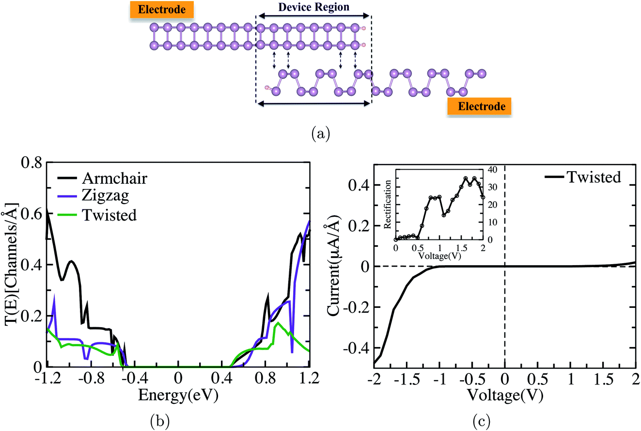 | ||
| Fig. 4 (a) Schematic picture of the twisted bilayer nanojunction (device region has bilayers of armchair and zigzag directions), (b) zero bias transmission for the nanojunctions, and (c) current–voltage characteristics for the twisted nanojunction device (inset shows the rectification ratio of the respective device). | ||
This symmetric current can be understood from the transmission function at ±1.8 V in the inset of Fig. 3(b). Overall transmission in the voltage window range has much less magnitude than that of the armchair junction. The transmission peak yields the transmission coefficient of 0.1 channels per Å in the armchair direction whereas in the zigzag direction it comes out to be only 0.005 channels per Å around the Fermi level, and a lower transmission value implies a lower current for the zigzag nanojunction as shown in Fig. 3(b). The anisotropy factor (Iarm/Izig) for the current in these two nanojunctions, which are in the mutually perpendicular direction, is around 40 at 2 eV bias. This anisotropy is lower than the reported value for the monolayer form of BP in two different directions. Kou et al.51 suggested that the current for monolayer BP in the armchair direction is 100 times higher than that for the zigzag direction.
Furthermore, we do not see current rectification in these two devices and this is quite expected due to the symmetric structure of the device. For better understanding of anisotropic transmission and current in the two different nanojunction devices, we plotted the eigenchannels for the respective devices at +1.8 V at the center of voltage window. Fig. 3(c) presents the eigenchannel for the armchair direction, which indicates that there are conductive states spread all over the junction area and also in between the layers. This implies better interlayer coupling and higher interlayer tunneling probability. There are edge state contributions but they are not significant in the eigenchannel of the armchair device. On the other hand good coupling at 1.8 V bias implies that the conduction band minimum (CBM) of the left electrode couples to the valence band maximum (VBM) of the right one, but also an induced state is created within the bilayer area, which is responsible for the Fano resonance in transmission. This induced state naturally disappears when contact area vanishes.
For the junction in the zigzag direction, the 1.8 V bias eigenchannel is localized all over the junction but it gets more localized at the lower layer, where it does not connect to the right electrode (last 4 rows of atoms in Fig. 3(d)). Also there are no interlayer states connecting the layers, so it reduces the probability of electron tunneling from one layer to the other. This explains the lower transmission and current in the zigzag direction. In fact, the eigenchannel in Fig. 3(d) looks qualitatively the same as the eigenchannel for the Fano state in the armchair direction: we see an incoming state at the upper BP sheet, and the induced state below. However, because the conducting state that couples the layers is not present on this junction, the state generates not a Fano, but Wigner-shaped tunneling resonance, which is clearly seen in the inset of Fig. 3(b) at 0 eV. There are possibilities to tune the anisotropy factor (Iarm/Izig) by increasing the junction, which will imply a bigger quantum well, as explained by Zhang et al.52 The levels in the well can tune the resonate tunneling of the electrons in-between the layers which can further tune the anisotropy factor of the system.
To further take full advantage of the anisotropic behavior of BP, we introduce a twisted nanojunction as shown in Fig. 4(a), where the band structure and DOS of the twisted layer system have already been explained above. Here, we again have the ML–BL–ML architecture but one of the monolayers is in the armchair direction and the other has the zigzag direction on the top of each other. The central region has a structure of a vertically stacked 90° twisted bilayer, which would be isotropic; until now we have twisted the nanojunction setup with additional semi-infinite electrodes in either directions. The upper layer has a zigzag transport direction and lower layer has an armchair transport direction, and both layers have one edge terminated with hydrogen. In our case of study we took a junction length of 12 Å. The zero bias transmission in Fig. 4(b) shows that the overall transmission is lower than that of the armchair and zigzag directions. This is due to the twisted layer, which has less interaction between the BP layers than that of the AA-stacked bilayer which is also clear from the band structure in Fig. 1. The transmission gap remains nearly the same for zigzag and armchair nanojunctions, which, in the case of the nanojunction device, is simply the gap of the monolayer BP electrodes.
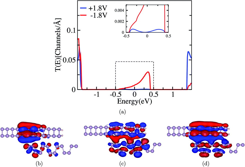
In this case, asymmetry is expected to bring in some rectification behavior; to check this, we increased the bias symmetrically over the junction with the step of 0.1 V. We contemplate a behavior in the I–V characteristics in Fig. 4(c), where current-rectifying properties can be seen. When the electrons are injected from the armchair to zigzag direction in a negative bias regime, the current is higher, whereas when it is injected from the zigzag to armchair direction, the current is lower. The inset of Fig. 4(c) shows a rectification ratio (I−/I+) with the maximum of 35 achieved at 1.8 V bias.
To understand the rectification behavior of the nanojunction, we further plot the transmission function at ±1.8 V bias, shown in Fig. 5(a), demonstrating high transmission probability for negative bias (−1.8 V) and much less transmission for positive bias (+1.8 V) in the bias window. In the negative bias, we notice the transmission at 0 eV but also a higher peak appears at 0.35 eV above the Fermi level. This difference in transmission for negative and positive bias arises from the different conductance in zigzag and armchair directions, the effect of which can be seen in Fig. 4(a and b).
 | ||
| Fig. 5 (a) Transmission at ±1.8 V bias for the twisted bilayer nanojunction (inset shows the zoomed picture of transmission at around 0 eV) and eigenchannels for the rotated bilayer nanojunction at 0 eV (b) at a positive bias of 1.8 V and (c) negative bias of 1.8 V and (d) eigenchannel at 0.35 eV at −1.8 V bias. | ||
Additionally we plot the eigenchannels for both the biases as ±1.8 V for 0 eV energy, shown in Fig. 5(b and c), which give information on quantum channels responsible for different current behaviours. It is quite obvious from the eigenchannels that for the negative bias there is strong tunneling probability from the armchair to zigzag layer as the channel is spread all over the device region which implies the higher conductance. In the positive bias (+1.8 V), the channel is more localized towards the left side of the nanojunction and remains only in the zigzag layer, which yields lower tunneling from the zigzag to armchair layer and provides the lower conductance. We have already discussed in Fig. 4(c) that in the negative bias, a higher transmission peak appears at +0.35 eV; henceforth it is worth plotting the eigenchannel at this energy, shown in Fig. 5(d). This presents a strong tunneling channel, delocalized all over the nanojunction area and responsible for much higher current in the negative bias regime.
The role of the edge states can be estimated from the results where the length (and the area) of the overlapped BP sheets was decreased, yielding a lower rectification ratio, see ESI Fig. S2,† where the length of different junctions has been explored for I–V characteristics. In this case the edge states play a significant role in the conductance mechanism, while rectification is mainly due to the interlayer tunneling. The increase of the junction length means a bigger quantum well and bigger length for interlayer tunneling which implies the higher rectification up to a certain limiting length. The length dependent rectifying properties can be the case of further study. Also the termination of edge can play an important role in defining the rectifying properties. Another limitation of our work is that we use BP as a lead to make simulations reasonably less expensive and reasonable. In experiment, one would inject electrons from metallic electrodes and also control the electrode's potentials through metal. We model such a situation via directly controlling the electrodes; the limitation is that we miss metal induced states, which might slightly affect the rectification ratio. This also suggests yet another method of controlling rectification by placing the junction asymmetrically with respect to the electrodes, which we do not explore.
It is very interesting to see the rectifying behavior in a device where no electron transfer between the layers and no band bending exist at the equilibrium state. This means that there is no standard p–n junction type of characteristics present at the beginning. Comparing the I–V characteristics of the rotated nanojunction with the armchair and zigzag nanojunction, it is evident that for the positive bias, when the electron flow is from the zigzag to armchair direction the limiting current regime is zigzag directional current. When the current flow is from the armchair to zigzag direction it follows the armchair nanojunction for limiting current.
A twisted bilayer has been reported for gate switchable transport anisotropy with applied gate voltage. We also report the gate tunable electronic structure of the twisted bilayer in Fig. S4,† where the out of plane gate voltage can tune the isotropic behavior of the band twisted bilayer in periodic form. Henceforth, we suggest that in the real time device electron transport behavior can be controlled by the applied gate voltage, which further opens the wide range of possibilities to tune the current and even yield much higher rectification which makes the setup desirable in nano-electronic applications. Although the stability of BP under ambient conditions is still a challenge, encapsulation of these kinds of devices is a popular technique to prevent them from degrading for a longer period.
In conclusion by using DFT along with NEGF calculations, we report a unique nanoscale rectifying device which consists of two phosphorene sheets in parallel contact with the 90° twisted angle without anything additionally bridging the electrodes. This rectifier is different from the widely explored other 2D heterostructure based p–n junctions. In those devices, band alignment and contact regions are important, while in this twisted stacked junction, band alignment is not a deciding parameter. We also studied two symmetric nanojunctions oriented along armchair and zigzag directions with different resistivities due to the anisotropy of the BP. We investigate the rectifying properties by using eigenchannels and their localization across the junction. No current rectification is observed in symmetric junctions, yet resistivities are different along different directions. In the asymmetric 90° twisted junction the electron flow along the “easy” direction is spread over the junction area, and electrons tunnel between overlapping layers, but also the induced state is seen as Fano resonance. Along the opposite direction, electrons are mostly reflected from the edge of the sheet, and tunneling of electrons from one layer to the other is inefficient and induced states start to play a foremost role in transport. Directional anisotropy is the only the reason behind this rectifying behavior of the device. Many tuning mechanisms can be foreseen for the BP device, like perpendicular electric field (through gate voltage), strain, asymmetric design and variable contact area. Our work further opens the possibilities for implementing field effect transistors or rectifiers. This is to our knowledge the first time when anisotropy in the system has been proposed to produce the rectifying behavior in nanojunction devices.
Methods
First principles density functional theory (DFT)53,54 calculations were performed using the SIESTA55,56 program within generalized gradient approximation with the Perdew, Burke and Ernzerhof (PBE)57 functional for geometrical optimization through total energy calculations. Norm-conserved Troullier–Martins pseudopotentials were used to describe the interaction between the core and valence electrons.58 The mesh cut off was 200 eV and Brillouin zone integration for the supercell was sampled by 2 × 2 × 1 k-points, and for a unit cell it was 20 × 30 × 1 within the Monkhorst–Pack scheme with a double-polarized basis set.59 To simulate the unit and super cell of bilayers, periodic boundary conditions were used with 30 Å vacuum space to minimize the interaction between the layers. The systems were fully relaxed to obtain the ground state structure with residual forces on the atoms less than 0.01 eV per atom. The quantum transport properties have been studied combining the non-equilibrium Green's function (NEGF) and DFT in the TranSIESTA60 module using a gamma k-point grid which yields reasonably converged results in comparison with the 1 × 4 k-point grid. The transmission spectrum, which defines the probability for electrons to be transferred from the left to right electrode with the specific energy E, is calculated from the equation,61| T(E,V) = tr[ΓR(E,V)GC(E,V)ΓL(E,V)G†C(E,V)] | (1) |
 | (2) |
Conflicts of interest
There are no conflicts of interest.Acknowledgements
The authors acknowledge computational resources provided through Swedish National Infrastructure for Computing (SNIC2019-1-25). VS acknowledges funding from the European Erasmus fellowship program. AG and RA acknowledge support from the Swedish Research Council.References
- A. K. Geim and I. V. Grigorieva, van der Waals heterostructures, Nature, 2013, 499, 419–425 CrossRef CAS PubMed.
- J. Zhang, W. Xie, J. Zhao and S. Zhang, Band alignment of two-dimensional lateral heterostructures, 2D Mater., 2016, 4, 015038 CrossRef.
- H. Yu, A. Kutana and B. I. Yakobson, Carrier delocalization in two-dimensional coplanar p–n junctions of graphene and metal dichalcogenides, Nano Lett., 2016, 16, 5032–5036 CrossRef CAS PubMed.
- A. K. Geim and K. S. Novoselov, The rise of graphene, Nat. Mater., 2007, 6, 183 CrossRef CAS PubMed.
- Y. Zhang, Y.-W. Tan, H. L. Stormer and P. Kim, Experimental observation of the quantum Hall effect and Berry's phase in graphene, Nature, 2005, 438, 201 CrossRef CAS PubMed.
- X. Xu, W. Yao, D. Xiao and T. F. Heinz, Spin and pseudospins in layered transition metal dichalcogenides, Nat. Phys., 2014, 10, 343 Search PubMed.
- Z. Gholamvand, D. McAteer, A. Harvey, C. Backes and J. N. Coleman, Electrochemical applications of two-dimensional nanosheets: the effect of nanosheet length and thickness, Chem. Mater., 2016, 28, 2641–2651 CrossRef CAS.
- V. Shukla, R. B. Araujo, N. K. Jena and R. Ahuja, The curious case of two dimensional Si2BN: a high-capacity battery anode material, Nano Energy, 2017, 41, 251–260 CrossRef CAS.
- N. K. Jena, R. B. Araujo, V. Shukla and R. Ahuja, Borophane as a benchmate of graphene: a potential 2D material for anode of Li and Na-ion batteries, ACS Appl. Mater. Interfaces, 2017, 9, 16148–16158 CrossRef CAS PubMed.
- V. Shukla, R. B. Araujo, N. K. Jena and R. Ahuja, Borophene's tryst with stability: exploring 2D hydrogen boride as an electrode for rechargeable batteries, Phys. Chem. Chem. Phys., 2018, 20, 22008–22016 RSC.
- R. Frisenda, A. J. Molina-Mendoza, T. Mueller, A. Castellanos-Gomez and H. S. van der Zant, Atomically thin p–n junctions based on two-dimensional materials, Chem. Soc. Rev., 2018, 47, 3339–3358 RSC.
- K. Novoselov, A. Mishchenko, A. Carvalho and A. C. Neto, 2D materials and van der Waals heterostructures, Science, 2016, 353, aac9439 CrossRef CAS PubMed.
- L. Esaki and R. Tsu, Superlattice and negative differential conductivity in semiconductors, IBM J. Res. Dev., 1970, 14, 61–65 CAS.
- R. B. Pontes, R. H. Miwa, A. J. da Silva, A. Fazzio and J. E. Padilha, Layer-dependent band alignment of few layers of blue phosphorus and their van der Waals heterostructures with graphene, Phys. Rev. B, 2018, 97, 235419 CrossRef CAS.
- J. Padilha, A. Fazzio and A. J. da Silva, van der Waals heterostructure of phosphorene and graphene: tuning the Schottky barrier and doping by electrostatic gating, Phys. Rev. Lett., 2015, 114, 066803 CrossRef CAS PubMed.
- M. Z. Iqbal, S. Siddique, M. F. Khan, A. u. Rehman, A. Rehman and J. Eom, Gate-Dependent Tunnelling Current Modulation of Graphene/hBN Vertical Heterostructures, Adv. Eng. Mater., 2018, 20, 1800159 CrossRef.
- D. Pierucci, H. Henck, J. Avila, A. Balan, C. H. Naylor, G. Patriarche, Y. J. Dappe, M. G. Silly, F. Sirotti, A. T. C. Johnson, M. C. Asensio and A. Ouerghi, Band Alignment and Minigaps in Monolayer MoS2-Graphene van der Waals Heterostructures, Nano Lett., 2016, 16, 4054–4061 CrossRef CAS PubMed.
- H.-P. Komsa and A. V. Krasheninnikov, Electronic structures and optical properties of realistic transition metal dichalcogenide heterostructures from first principles, Phys. Rev. B: Condens. Matter Mater. Phys., 2013, 88, 085318 CrossRef.
- D. Li, M. Chen, Z. Sun, P. Yu, Z. Liu, P. M. Ajayan and Z. Zhang, Two-dimensional non-volatile programmable p–n junctions, Nat. Nanotechnol., 2017, 12 9, 901–906 CrossRef PubMed.
- M. A. Khan, S. Rathi, C. Lee, Y. Kim, H. Kim, D. Whang, S. J. Yun, D.-H. Youn, K. Watanabe, T. Taniguchi and G.-H. Kim, High performance self-gating graphene/MoS2 diode enabled by asymmetric contacts, Nanotechnology, 2018, 29, 395201 CrossRef PubMed.
- M. S. Choi, D. Qu, D. Lee, X. Liu, K. Watanabe, T. Taniguchi and W. J. Yoo, Lateral MoS2 p–n junction formed by chemical doping for use in high-performance optoelectronics, ACS Nano, 2014, 8, 9332–9340 CrossRef CAS PubMed.
- J.-W. Chen, et al., A gate-free monolayer WSe2 pn diode, Nat. Commun., 2018, 9, 3143 CrossRef PubMed.
- C. Jin, J. Kim, J. Suh, Z. Shi, B. Chen, X. Fan, M. Kam, K. Watanabe, T. Taniguchi, S. Tongay, A. Zettl, J. Wu and F. Wang, Interlayer electron–phonon coupling in WSe2/hBN heterostructures, Nat. Phys., 2017, 13, 127–131 Search PubMed.
- C.-H. Lee, G.-H. Lee, A. M. van der Zande, W. Chen, Y. Li, M. Han, X. Cui, G. Arefe, C. Nuckolls, T. F. Heinz, J. Guo, J. Hone and P. Kim, Atomically thin p–n junctions with van der Waals heterointerfaces, Nat. Nanotechnol., 2014, 9, 676–681 CrossRef CAS PubMed.
- E. Ponomarev, N. Ubrig, I. Gutiérrez-Lezama, H. Berger and A. F. Morpurgo, Semiconducting van der Waals Interfaces as Artificial Semiconductors, Nano Lett., 2018, 18(8), 5146–5152 CrossRef CAS PubMed.
- Q. Liu, G. Luo, R. Qin, H. Li, X. Yan, C. Xu, L. Lai, J. Zhou, S. Hou, E. Wang, Z. Gao and J. Lu, Negative differential resistance in parallel single-walled carbon nanotube contacts, Phys. Rev. B: Condens. Matter Mater. Phys., 2011, 83, 155442 CrossRef.
- D. J. Leech, J. J. Thompson and M. Mucha-Kruczyński, Negative differential resistance in van der Waals heterostructures due to moiré-induced spectral reconstruction, Phys. Rev. Appl., 2018, 10, 034014 CrossRef CAS.
- L. Li, Y. Yu, G. J. Ye, Q. Ge, X. Ou, H. Wu, D. Feng, X. H. Chen and Y. Zhang, Black phosphorus field-effect transistors, Nat. Nanotechnol., 2014, 9, 372 CrossRef CAS PubMed.
- H. O. Churchill and P. Jarillo-Herrero, Two-dimensional crystals: phosphorus joins the family, Nat. Nanotechnol., 2014, 9, 330 CrossRef CAS PubMed.
- H. Liu, A. T. Neal, Z. Zhu, Z. Luo, X. Xu, D. Tománek and P. D. Ye, Phosphorene: an unexplored 2D semiconductor with a high hole mobility, ACS Nano, 2014, 8, 4033–4041 CrossRef CAS PubMed.
- M.-W. Lin, L. Liu, Q. Lan, X. Tan, K. S. Dhindsa, P. Zeng, V. M. Naik, M. M.-C. Cheng and Z. Zhou, Mobility enhancement and highly efficient gating of monolayer MoS2 transistors with polymer electrolyte, J. Phys. D: Appl. Phys., 2012, 45, 345102 CrossRef.
- A. Rodin, A. Carvalho and A. C. Neto, Strain-induced gap modification in black phosphorus, Phys. Rev. Lett., 2014, 112, 176801 CrossRef CAS PubMed.
- R. Fei and L. Yang, Strain-engineering the anisotropic electrical conductance of few-layer black phosphorus, Nano Lett., 2014, 14, 2884–2889 CrossRef CAS PubMed.
- D. Çakır, H. Sahin and F. M. Peeters, Tuning of the electronic and optical properties of single-layer black phosphorus by strain, Phys. Rev. B: Condens. Matter Mater. Phys., 2014, 90, 205421 CrossRef.
- S. P. Koenig, R. A. Doganov, H. Schmidt, A. Castro Neto and B. Özyilmaz, Electric field effect in ultrathin black phosphorus, Appl. Phys. Lett., 2014, 104, 103106 CrossRef.
- Y. Deng, Z. Luo, N. J. Conrad, H. Liu, Y. Gong, S. Najmaei, P. M. Ajayan, J. Lou, X. Xu and P. D. Ye, Black phosphorus–monolayer MoS2 van der Waals heterojunction p–n diode, ACS Nano, 2014, 8, 8292–8299 CrossRef CAS PubMed.
- L. Huang, N. Huo, Y. Li, H. Chen, J. Yang, Z. Wei, J. Li and S.-S. Li, Electric-field tunable band offsets in black phosphorus and MoS2 van der Waals pn heterostructure, J. Phys. Chem. Lett., 2015, 6, 2483–2488 CrossRef CAS PubMed.
- L. Huang and J. Li, Tunable electronic structure of black phosphorus/blue phosphorus van der Waals pn heterostructure, Appl. Phys. Lett., 2016, 108, 083101 CrossRef.
- J. Qiao, X. Kong, Z.-X. Hu, F. Yang and W. Ji, High-mobility transport anisotropy and linear dichroism in few-layer black phosphorus, Nat. Commun., 2014, 5, 4475 CrossRef CAS PubMed.
- D. Çakır, C. Sevik and F. M. Peeters, Significant effect of stacking on the electronic and optical properties of few-layer black phosphorus, Phys. Rev. B: Condens. Matter Mater. Phys., 2015, 92, 165406 CrossRef.
- V. Tran, R. Soklaski, Y. Liang and L. Yang, Layer-controlled band gap and anisotropic excitons in few-layer black phosphorus, Phys. Rev. B: Condens. Matter Mater. Phys., 2014, 89, 235319 CrossRef.
- S. Das, W. Zhang, M. Demarteau, A. Hoffmann, M. Dubey and A. Roelofs, Tunable transport gap in phosphorene, Nano Lett., 2014, 14, 5733–5739 CrossRef CAS PubMed.
- S. Lei, H. Wang, L. Huang, Y.-Y. Sun and S. Zhang, Stacking Fault Enriching the Electronic and Transport Properties of Few-Layer Phosphorenes and Black Phosphorus, Nano Lett., 2016, 16, 1317–1322 CrossRef CAS PubMed.
- C. Sevik, J. R. Wallbank, O. Gülseren, F. M. Peeters and D. Çakır, Gate induced monolayer behavior in twisted bilayer black phosphorus, 2D Mater., 2017, 4, 035025 CrossRef.
- T. Cao, Z. Li, D. Y. Qiu and S. G. Louie, Gate Switchable Transport and Optical Anisotropy in 90° Twisted Bilayer Black Phosphorus, Nano Lett., 2016, 16, 5542–5546 CrossRef CAS PubMed.
- J. Xie, Q. Luo, L. Jia, Z. Zhang, H. Shi, D. Yang and M. Si, Strain-induced recovery of electronic anisotropy in 90°-twisted bilayer phosphorene, Europhys. Lett., 2018, 121, 27002 CrossRef.
- T. A. Ameen, H. Ilatikhameneh, G. Klimeck and R. Rahman, Few-layer Phosphorene: An Ideal 2D Material For Tunnel Transistors, Sci. Rep., 2016, 6, 28515 CrossRef CAS PubMed.
- P. Kang, W.-T. Zhang, V. Michaud-Rioux, X.-H. Kong, C. Hu, G.-H. Yu and H. Guo, Moiré impurities in twisted bilayer black phosphorus: effects on the carrier mobility, Phys. Rev. B, 2017, 96, 195406 CrossRef.
- M. Dion, H. Rydberg, E. Schröder, D. C. Langreth and B. I. Lundqvist, Van der Waals Density Functional for General Geometries, Phys. Rev. Lett., 2004, 92, 246401 CrossRef CAS PubMed.
- J. Klimeš, D. R. Bowler and A. Michaelides, Chemical accuracy for the van der Waals density functional, J. Phys.: Condens. Matter, 2009, 22, 022201 CrossRef PubMed.
- L. Kou, T. Frauenheim and C. Chen, Phosphorene as a superior gas sensor: selective adsorption and distinct I–V response, J. Phys. Chem. Lett., 2014, 5, 2675–2681 CrossRef CAS PubMed.
- J. Zhang, W. Xie, M. L. Agiorgousis, D.-H. Choe, V. Meunier, X. Xu, J. Zhao and S. Zhang, Quantum oscillation in carrier transport in two-dimensional junctions, Nanoscale, 2018, 10, 7912–7917 RSC.
- P. Hohenberg and W. Kohn, Inhomogeneous electron gas, Phys. Rev., 1964, 136, B864 CrossRef.
- W. Kohn and L. J. Sham, Self-consistent equations including exchange and correlation effects, Phys. Rev., 1965, 140, A1133 CrossRef.
- J. M. Soler, E. Artacho, J. D. Gale, A. García, J. Junquera, P. Ordejón and D. Sánchez-Portal, The SIESTA method for ab initio order-N materials simulation, J. Phys.: Condens. Matter, 2002, 14, 2745 CrossRef CAS.
- E. Artacho, E. Anglada, O. Diéguez, J. D. Gale, A. García, J. Junquera, R. M. Martin, P. Ordejón, J. M. Pruneda, D. Sánchez-Portal and J. M. Soler, The SIESTA method; developments and applicability, J. Phys.: Condens. Matter, 2008, 20, 064208 CrossRef PubMed.
- J. P. Perdew, K. Burke and M. Ernzerhof, Generalized gradient approximation made simple, Phys. Rev. Lett., 1996, 77, 3865 CrossRef CAS PubMed.
- N. Troullier and J. L. Martins, Efficient pseudopotentials for plane-wave calculations. II. Operators for fast iterative diagonalization, Phys. Rev. B: Condens. Matter Mater. Phys., 1991, 43, 8861 CrossRef PubMed.
- H. J. Monkhorst and J. D. Pack, Special points for Brillouin-zone integrations, Phys. Rev. B: Solid State, 1976, 13, 5188 CrossRef.
- M. Brandbyge, J.-L. Mozos, P. Ordejón, J. Taylor and K. Stokbro, Density-functional method for nonequilibrium electron transport, Phys. Rev. B: Condens. Matter Mater. Phys., 2002, 65, 165401 CrossRef.
- S. Datta, Electronic Transport in Mesoscopic Systems, Cambridge University Press, 1997 Search PubMed.
Footnote |
| † Electronic supplementary information (ESI) available: Experimental procedures and characterization data for all new compounds. See DOI: 10.1039/c9na00320g |
| This journal is © The Royal Society of Chemistry 2020 |