
 Open Access Article
 This Open Access Article is licensed under a Creative Commons Attribution-Non Commercial 3.0 Unported Licence
Great chiral fluorescence from the optical duality of silver nanostructures enabled by 3D laser printing†
Hongjing
Wen‡
 ab,
Shichao
Song‡
a,
Fei
Xie
a,
Bin
Wang
b,
Jian
Xu
a,
Ziwei
Feng
a,
Shiyu
Wu
a,
Jing
Han
a,
Bai-Ou
Guan
a,
Xiaoxuan
Xu
*b,
Yaoyu
Cao
*a and
Xiangping
Li
a
ab,
Shichao
Song‡
a,
Fei
Xie
a,
Bin
Wang
b,
Jian
Xu
a,
Ziwei
Feng
a,
Shiyu
Wu
a,
Jing
Han
a,
Bai-Ou
Guan
a,
Xiaoxuan
Xu
*b,
Yaoyu
Cao
*a and
Xiangping
Li
a
aGuangdong Provincial Key Laboratory of Optical Fiber Sensing and Communications, Institute of Photonics Technology, Jinan University, Guangzhou 511443, P. R. China. E-mail: yaoyucao@jnu.edu.cn
bThe Key Laboratory of Weak-Light Nonlinear Photonics, Ministry of Education, School of Physics, Nankai University, Tianjin 300071, China. E-mail: xuxx@nankai.edu.cn
First published on 20th October 2020
Abstract
Featured by prominent flexibility and fidelity in producing sophisticated stereoscopic structures transdimensionally, three-dimensional (3D) laser printing techniques have vastly extended the toolkit for delivering diverse functional devices. Yet chiral nanoemitters heavily resorting to artificial structures that manifest efficient emission and tightly confined light–matter interactions simultaneously remain alluring but dauntingly challenging for this technique at this moment. In this study, we assert that the chiral photoluminescence is implemented from silver nanostructures with optical duality in one go via a two-fold three-dimensional laser printing scheme. Such laser printing protocol allows the highly desired duality by simultaneously producing uniformly distributed fluorescent silver nanoclusters and aggregated plasmonic silver nanoparticles to tightly confine chiral interactions at the nanoscale. A helical emitter of 550 nm helix-diameter as fabricated has seen a record-high luminescence anisotropic factor with the absolute value up to 0.58, which is two orders of magnitude greater than fluorescent chiral silver clusters. This method holds great promise for future versatile applications in chiroptical nanodevices.
New conceptsThe exceptional capabilities of 3D laser printing techniques have been continuously explored to extend the toolkits for advancing transdimensional photonic and optoelectronic applications in the past few decades. Nevertheless, the limitation arising from the lack of multifunctional materials and the corresponding printing protocols greatly bars the efforts in the subwavelength scale for elaborately delivering the chiral regulation of electromagnetic waves over the short-wavelength bands, which is highly desirable in the fields of frontier optics and photonics. Chiral nanoemitters heavily resorting to artificial structures that manifest efficient emission and tightly confined light–matter interactions simultaneously remain alluring but dauntingly challenging for this technique at this moment. In this work, we have developed a 3D laser printing technique for realizing unprecedented stereo chiral luminescent silver nanostructures comprising plasmonic nanostructures and emissive clusters in one go. The as-fabricated helical silver emitter of 550 nm helix-diameter, as a representative of 3D chiral structure family, has seen a record-high luminescence anisotropic factor with an absolute value up to 0.58, which is two orders of magnitude greater than that of fluorescent chiral silver clusters (10−3). We believe that our work could greatly inspire the advance of 3D laser printing approach for exploring its applications in producing functional nanodevices. |
Introduction
Chiral nanoemitters currently have attracted drastically increasing research interests for their abilities to underpin cutting-edge applications spanning the advanced optical and photonics,1–4,41,42 such as manipulating energy transfer among topologically configured photonic systems5 and controlling communication with spin information.6 Such functionalities and applications intensely rely upon implementing strong light–matter interactions in the nanoscale,7,41 which requires extremely confined interacting space to achieve demanding chiral luminescence that is not always applicable to the natural chiral materials with a common anisotropic factor at the level of 0.001.8 Consequently, the advance of such chiral light sources preferably seeks artificial materials generated through a deterministic nanofabrication technique with considerable printing freedom in favor of offering efficient emitters and tight light–matter interaction confinement at the same time.3D laser printing, as one of the most important and fascinating technological innovations,9–12 has proven to be an indispensable micro/nanofabrication technique to shape multiple materials by employing their intrinsic optical nonlinear responses,13–17 such as multi-photon photoredox (MPP)16 and two-photon polymerization (TPP),18–20 reversible printing/erasing.43,44 During the past few decades, the printing strategy that achieves ultrahigh spatial resolution21 has been used to additively create a myriad of functionalized structures for advanced nanoscale photonic and optoelectronic applications.22,23,43 The flexibilities and fidelities rooted in the technique add vast advantages to arbitrarily and precisely producing stereo architectures for spatially manipulating electromagnetic field.24 Nevertheless, most of these achievements feature with producing structures based on materials with mono-characteristic supremely well.25 The limitation arising from the lack of multifunctional materials and the corresponding printing protocols greatly bars the efforts in the subwavelength scale for elaborately delivering chiral regulation of radiative electromagnetic waves over the short wavelength bands and exploring unparalleled optoelectronic properties.
In this article, we propose and demonstrate a photoreduction-based additive laser printing scheme to categorically achieve chiral luminescence with 3D silver nanostructures of optical duality in one go within agarose hydrogel, where the anisotropic factor of the photoluminescence with absolute value can reach up to 0.58 for a single emitter. The silver nanoclusters with the average size amid the mesoscopic scale between isolated metal atoms and metallic nanoparticles26–28 can be precisely produced by laser-induced photoreduction of silver ions for light emission with its spectrum consistent with previous reports,29–31 whilst the silver nanostructure composed of assembled silver nanoparticles can be simultaneously fabricated to offer a delicate platform for the helicity control in the visible wavelength region with a surface plasmon effect.32,33 As such, the twofold laser printing protocol can readily create nanoemitters with steered luminescence through programmably forming two types of silver nanofeatures at the same time. The feasibility of this printing scheme is strongly bolstered by the use of the agarose matrix that renders both pore grids and electron donors for fixing the silver nanoemitters and assisting the silver photoreduction, respectively. By producing glowing silver nanoclusters and fabricating spiral-shape nanostructures synchronously, silver nanocluster-based nanostructures with regulated photoluminescence and chiral properties are realized with multiple complexities. With the aid of plasmonic helical structures, the photoemission process of silver nanoclusters can be deeply guided to follow the structural symmetries. The absolute value of the highest anisotropic factor can reach up to ∼0.58 at 675 nm, manifesting extraordinary chiral photoluminescence characteristic with the value two orders of magnitude greater than fluorescent chiral silver clusters.34 Moreover, the theoretical calculations confirm the observation of circular dichroism (CD) and anisotropic factor of the emitter, which opens up exceptional perspectives for delivering versatile applications in chiroptical nanodevices.
Results and discussion
As an appealing platform for hosting the production of silver nanostructures, water-soluble agarose offers a homogenous circumstance for the reactants to stably photosynthesize silver nanoclusters (SNCs) and silver nanoparticles (SNPs) in the interior of the gel. The size-tunable pore structures of agarose,35 conducive to the aggregation and formation of silver nanofeatures, could scaffold 3D consecutive silver nanocluster-based structures in effect, as shown in Fig. 1(a–c) (the scanning electron microscopic image of agarose can be seen in Fig. S1 (ESI†)). Moreover, taking advantages of multiple hydroxy groups of electron donor ability linked to the scaffoldings, agarose can aid the generation of SNCs and SNPs through anionic surfactant-assisted redox reactions16 superior to its hydrogel counterparts (seen in Fig. S2 (ESI†)). Herein, SNCs and SNPs are simultaneously photoreduced from silver ions for light emission and light manipulation, respectively, as shown in Fig. 1d. Eventually, the stable silver nanostructures composed of varisized SNCs and SNPs will be obtained tracing the printing path. | ||
| Fig. 1 Stereo silver nanocluster-based structure via 3D laser printing. (a) Schematic of the formation of fluorescent silver helical structures in the agarose matrix via 532 nm femtosecond laser printing and the chiral fluorescence generated from the silver structures excited by 532 nm continuous wave laser. (b) Dark-field images of a 3-turn helical structure with a radius of 5 μm and a pitch distance of 5 μm in the agarose matrix. The top view of the helix is on the left, while the side view is on the right. The scale bars are 10 μm. (c) Confocal fluorescence images corresponding to the 3D spiral structure of (b) in top view (left) and side view (right) at a certain focal plane. The scale bars are 10 μm. (d) TEM image of a single silver dot composed of SNCs (with sizes below 10 nm) and SNPs (with sizes over 10 nm) with different sizes in agarose. The scale bar is 100 nm. (e) Size statistical distribution of SNCs inside the silver dotted structure in (d). The nano-entities with an intense fluorescence effect below 2 nm account for ∼20% out of the total SNCs. (f) Standard deviation (SD) and the root mean square (RMS) of the scattering intensity variance along the silver line fabricated in agarose with different mass-to-volume ratios (with details shown in Fig. S3 (ESI†)). Insets are the corresponding dark-field images of the lines as printed. The scale bars are 10 μm. | ||
The size distribution of the SNCs and SNPs is gauged using the transmission electron microscopic (TEM) image of a silver dot fabricated in an agarose matrix with a laser power of 1 mW and an exposure time of 80 ms. SNCs less than 2 nm in size with superior luminescence ability28 account for about 20% of nanofeatures below 10 nm where the statistical average size is about 4 nm, as depicted in Fig. 1(d and e). In general, the photoreduction of silver ions are conducted by the photoexcitation of electron donors, i.e., free radicals, with femtosecond pulses, for producing SNCs and SNPs. Consequently, a lump of assembled SNPs with the size of around 300 nm can be obtained in the central region, as a result of intense light field boosted series of chemical and physical reactions including photoreduction, trapping and coalescence, which suggests the photoreduced silver particle may undergo a rapid growth either by further photoreduction of silver ions on its surface or aggregation of different silver nanoclusters. Meanwhile, few-nanometer SNCs, formed amid the photoreduction of a small amount of silver ions followed by localized assembling process, can be found either attaching onto the surface of a few larger SNPs like a shell or scattering nearby the core base on the TEM image, which may give rise to a hybrid optical property. To improve the uniformity of the assembled SNPs, we investigated the light scattering intensity distribution of the silver lines as fabricated with varying agarose contents in terms of mass–volume ratio. As shown in Fig. 1f, an inverse correlation between the scattering intensity variance and the scaffolding density can be found with the standard deviation and the root mean square analysis. Nevertheless, while the content of agarose exceeded 7% w/v, the silver ammonia solution exhibited difficulties in spreading into the agarose matrix. Thus, we opted for the mass–volume ratio of 7% for the scaffolding matrix in the subsequent experiments. (The detailed data are shown in Fig. S3 (ESI†).) Through computer-aided laser scanning, a rigid three-dimensional luminescent silver nanocluster-based helical structure can be successfully fabricated within the three-dimensional pore grids of agarose matrix. Fig. 1(b and c) clearly display the rigid scattering and luminescence patterns arising from the excitation of SNPs and SNCs, respectively, which refers to the surface plasmon effect and the irradiation process accordingly.
To investigate the optical irradiation properties of the luminescent silver structures, silver dots composed of SNCs and SNPs as elementary building blocks were adopted. As shown in Fig. 2a, the luminescence and scattering intensities of a dotted structure produced with the 532 nm-fs laser beam of power (Plp) 1 mW were measured in situ with the spectral range of 600 nm to 800 nm (red line). The emission lifetime of the silver dot was gauged below 0.5 ns, which implies a fast luminescence process (Fig. S4a (ESI†)). The bright fluorescence occurring in the whole printing region reveals that the SNCs spread over the silver dot as shown in the fluorescence image captured via the confocal microscope. In the meantime, the scattering spectrum of the silver dot shows the light can be strongly scattered in the same range as a result of surface plasmon effect. The measured scattering peak virtually coincides with the simulation result, where the broader scattering band in the experimental spectrum can be attributed to the effective silver dot composed of varisized SNPs that can be seen in Fig. S4(b and c) (ESI†). Moreover, the polarization of fluorescence from the silver dot was also studied. A linear polarizer (LP) was added into the fluorescence-collecting system to manifest the polarization characteristic of emission through changing the analyzer angles.36 To avoid the disturbance from the analyzing system, rhodamine 6G (R6G) with unpolarized fluorescence was introduced into the agarose matrix system as a reference. Consequently, the relative intensity variation of fluorescence (Vf) emitted from the silver dot with the analyzer rotation angle θ can be defined as Vf = (Idot(θ) − IR6G(θ))/(Idot(0°) − IR6G(0°)), where Idot(0°) and IR6G(0°) are the fluorescence intensities of the dot and R6G reference with an initial polarization analyzer angle of 0°, respectively. Idot(θ) and IR6G(θ) denote the fluorescence intensities of the dot and R6G reference with a rotated angle θ, respectively. As depicted in Fig. 2b, the virtually unchanged Vf value at around 1 measured at ∼630 nm represents that the structure possesses an unpolarized electromagnetic response, indicating the silver nanocluster fluorescence of non-polarizing characteristic (the measured fluorescence spectra with different polarization angles θ can be seen in Fig. S5 (ESI†)).
 | ||
| Fig. 2 Optical duality of silver nanopatterns. (a) Scattering spectrum and fluorescence spectrum excited by 532 nm CW laser of a silver dotted structure. The insets depict the dark-field image and the confocal fluorescence microscopic image of the silver dotted structure fabricated in agarose with a laser power (Plp) of 1 mW and an exposure time of 80 ms. The scale bars are 2 μm. (b) Relative variation V of fluorescence intensity emitted from silver dots with different polarization angles. (c) Fluorescence emission spectra of silver nanodots printed with different Plp (from 0.6 to 1.4 mW). (d) The corresponding fluorescence intensity (red ball scatters) at a wavelength of 630 nm (black dot line in (c)), the scattering intensity (green ball scatters) and dot diameter (blue ball scatters) under different printing powers. (e) Dark-field image of a 4 × 4 silver dot lattice with a printing power of 1 mW and exposure time of 80 ms for each dot. In addition, the corresponding scattering intensities along the two white dashed line marks are depicted in the nether figures, which show favorable uniformity of the lattice structure. The scale bar is 5 μm. (f) Fluorescence image of the 4 × 4 silver dot lattice; the corresponding fluorescence intensities of the two white marked areas are depicted in the nether figures, which show reasonable uniformity of photoluminescence. The scale bar is 5 μm. | ||
To further explore the fluorescence and scattering intensity with regard to the size of a single pixel as fabricated, a series of dotted structures were realized with different laser powers Plp ranging from 0.6 to 1.4 mW. In addition, the feature sizes of the silver dotted structure measured using the dark-field images can be found in the range from 380 nm to 830 nm. In effect, the fluorescence intensities were positively correlated with the dimensions of silver dots, as shown in Fig. 2c. In the meantime, we can find that the variance in scattering intensity follows a similar tendency, indicating a reinforced ability of light manipulation with the increase in the printing power, where the measured dark-field images of silver dotted structures corresponding to fluorescence spectra are presented in Fig. S6a (ESI†). As shown in Fig. 2d, a virtually linear relevance between the fluorescence intensity, the scattering intensity and the silver dot size can be found with the increase in the printing power from 0.8 mW to 1.2 mW, revealing a single photon characteristic for the generation of silver dots as well as the corresponding optical properties in the particular printing power region. Fluorescence emission spectra of a silver nanodot in the agarose matrix obtained with CW laser excitation can be seen in Fig. S6(b and c) (ESI†). In addition, the accumulation rate of the dot size and the related optical responses can be found to be slowing down with the further increase in printing laser power, which may arise from the depletion of the silver salts in the fabrication region.
In order to investigate the uniformity of the fluorescence and the surface plasmon-based scattering from silver structures, we fabricated a 4 × 4 silver dot lattice with a laser power of 1 mW and an exposure time of 80 ms. The corresponding dark-field image (Fig. 2e) and fluorescence image (Fig. 2f) measured by confocal fluorescence microscopy reveal a homogenous feature for the dot pattern. As it mainly comes from the SNPs, the steady high scattering intensity from dot to dot reflects the glorious uniformity between each dot unit and a powerful light manipulation ability of assembled SNPs as produced resorting to the surface plasmon effect, which can be obtained through the dashed mark line 1 and 2. Additionally, the uniformity of fluorescence is estimated through the dashed mark line 3 and 4, and emission intensity fluctuations are less than 10%, which further confirms the favorable homogeneity of SNCs as produced simultaneously.
Harnessing multiphoton absorption characteristic, silver ions in the agarose hydrogel are photoreduced to form spatially resolved arbitrary silver structures by the computer-aided printing with assembled SNPs and SNCs for effective light manipulation and fluorescence, respectively. In the meantime, the fluorescence intensity of the demonstrated structures can also be regulated by adjusting fabrication parameters such as the laser intensity. As shown in Fig. 3a, dark-field image (left upper green graphs) and confocal fluorescence microscope image (left nether red graphs) of the 2D dolphin pattern confirm the feasibility of the steady patterning. Besides, the right side shows the variation of scattering intensity and fluorescence intensity from the patterns depending on the printing power corresponding to the subregions in the left side. In this case, the fluorescence of the corresponding pattern was excited by 532 nm CW laser with an excitation power of 200 μW so as to ensure that the fluorescence will not be ablated. With a multilayer point-by-point printing approach, a homogeneous layered structure with an interlayer spacing of 5 μm can be explicitly fabricated and resolved in both dark-field images and confocal fluorescence microscope images, presented in Fig. 3b. Furthermore, by implementing the 3D vector scanning scheme, a cubic scaffold with continuous sides can be readily achieved, as shown in Fig. 3c. The corresponding dark-field images in the perspective view and top view indicate the high continuity of the stereo structure as a result of accurately assembling SNPs as supposed. The confocal images in perspective view are acquired by stitching layer records (the detailed layer-by-layer scanning images can be found in Fig. S7 (ESI†)). While a bit fluctuation of confocal fluorescence intensity in the perspective view comes from the image mosaic errors during the multilayer scanning, the fluorescence intensity distribution in the top view reveals reasonable uniformity for the same layer. Herein, eight lines are marked in the top view of the confocal fluorescence image to verify the uniformity of the 3D continuous structures. As shown in Fig. 3d, the fluctuation of fluorescence peak intensity is less than 10%, indicating considerable continuity and uniformity of the stereo structure, which is in favor of achieving versatile fluorescent nanostructures.
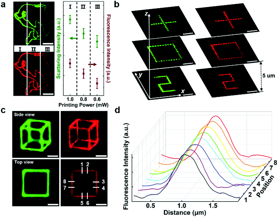 | ||
| Fig. 3 Structuring and patterning of 3D fluorescent silver nanocluster-based structures. (a) A dolphin pattern fabricated by three different printing powers (1.0 mW for the subregion I, 0.8 mW for the subregion II and 0.6 mW for the subregion III). In the left side, the left upper green graphs (false-color images) are the dark-field scattering image and the left nether red ones are the confocal fluorescence image. The right side shows the variation in the scattering intensity and fluorescence intensity from the patterns depending on the printing power corresponding to the subregions in the left side. (b) Dark-field (left) and fluorescence (right) images of three layers of silver patterns printed with a layer spacing of 5 μm. (c) Dark-field (left) and fluorescence (right) images of the 3D cubic structure fabricated in the agarose matrix on side view and top view, respectively. (d) Fluorescence intensity distribution tracing the white short lines marked at eight positions on the top of the cubic structure in (c). All the scale bars are 5 μm. | ||
As a representative three-dimensional structure with chirality, the helix possesses vast polarization manipulation capabilities for realizing circular dichroism (CD) and optical rotations.4,37 Taking full advantages of the chirality of the helical structure and photoluminescence of SNCs, fluorescence chiral structures can be realized in agarose by utilizing the joint characteristics from the inherent structural uniqueness of SNP spiral lines and fluorescence spectrum attribute of SNCs. To characterize the chirality of the helical structure, CD is defined as the difference between the fluorescence intensity with left-handed circular polarization (LCP) and right-handed circular polarization (RCP), which can be calculated using the following equation:
| CD = TLCP(λ) − TRCP(λ) | (1) |
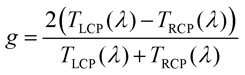 | (2) |
As illustrated in Fig. 4(a–d), a 2-turn left-handed helical structure with a helix diameter of 550 nm and a pitch of 550 nm in the z direction was fabricated with a laser power of 0.1 mW and a printing speed of 1 μm s−1. The scattering images of the helical structure on the top view and side view are snatched using a confocal microscope, as presented in Fig. 4(a and c). The linewidth of the spiral line in the helical structure was measured by the full width at half maximum (FWHM) of the scattering intensity peak at ∼200 nm in horizontal orientation and ∼340 nm in longitudinal direction, as shown in Fig. 4(b and d) (more helical structures with different parameters can be found in Fig. S8 (ESI†)).
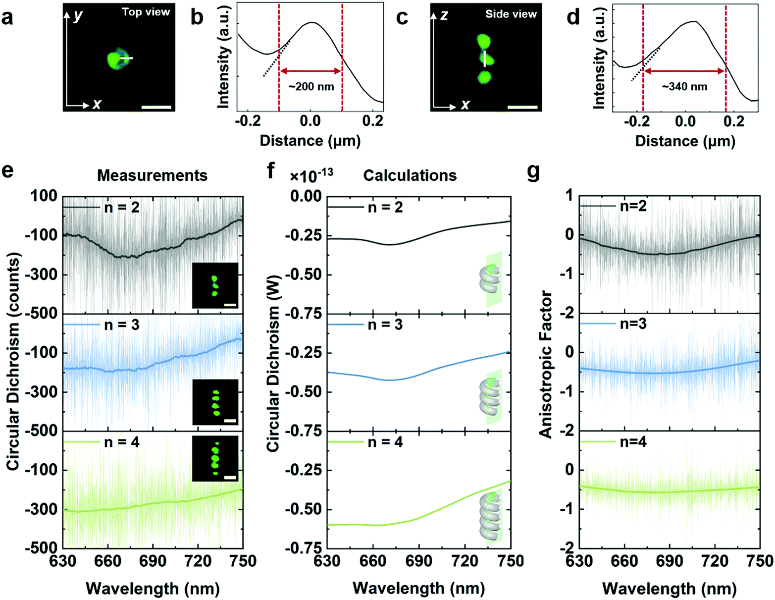 | ||
| Fig. 4 Chiral fluorescence of silver nanocluster-based helical nanostructures. (a) Top-view scattering image of a silver nanocluster-based helical structure (n = 2) captured using a confocal microscope. (b) Linewidth of the spiral line for the helical structure (obtained at the FWHM) was measured as ∼200 nm in the horizontal orientation. (c) Scattering image of the side view of the helical structure. (d) Linewidth of the spiral line of the helical structure was measured as ∼340 nm in the longitudinal direction. (e) Experimental results of CD for single silver nanoemitters with the helix turns ranging from 2 to 4. The insets are the scattering images of the cross-section profiles. (f) Calculated CD values normalized to the emission intensity of the dipoles used in the FDTD method (the inset is the simulation model set up with the same parameters obtained in experiments: helix diameter of 550 nm and pitch of 550 nm in the z direction). The corresponding models in calculations are shown in insets, and the green plane represents the measured plane with respect to (e). (g) Measured anisotropic factor spectra for single silver nanoemitters obtained with different turns of the helical structures. All the scale bars are 1 μm. | ||
The most prominent helicity characteristic of the helical structure relies on the repeated circles along the helical axial. By gradually changing the turns from n = 2 to 4, we can accordingly tune the structural chirality, where the corresponding CD spectra can be obtained by exciting the luminescence at the far-end of the emitters to the detector. As shown in Fig. 4e, the bands of the CD undergo manifest broadening over the wavelength measurement range of 630 nm to 750 nm with the increase in turns of the helical structure, while the maximum absolute value of CD increases gradually from 204 to 315. In addition, the fluorescence CD of the emitter clearly reveals a wavelength-dependence property. We can find that the CD value of the helical structure could dwindle more than 50% as the fluorescence of the emitter drops in the long-wavelength region.
To investigate the chirality functioning mechanism of silver helical nanostructures as fabricated, the finite difference time domain (FDTD) method is utilized with the dipole sources as the radiative origins of fluorescence and the power profile monitors for collecting the energy flux through the helical structures, where the spans of the monitors are in line with the objective aperture used in the experiment (more minutiae about the simulation settings are shown in Fig. S9 (ESI†)). Through elaborately building the silver structure models, the intensity of the transmitted LCP and RCP light can be extracted separately (the experiment and calculation results of LCP and RCP light are shown in Fig. S10 (ESI†)). As revealed in Fig. 4f, we can verify the broadening CD peak with the increase in helix turn, which may be attributed to the formation of multiple modes stemming from the structural plasmonic resonance.37 Moreover, the calculations possess a coordinating tendency sticking to the measured CD spectra, which confirms that the fluorescent silver nanohelix can afford a favorable chiral fluorescence. While the simplified silver helical structure model used in the simulations with ideally smoothed outer surface renders a slightly flat spectral response, the varisized silver nanoparticles existing on the surface of helical structures in practice may cause diverse localized plasmonic resonances, resulting in fluctuated CD values.
In order to further characterize the chirality of the silver nano-helix, the structural anisotropic factors of the fluorescence varying with wavelength can be obtained through gauging the transmittance of the LCP and RCP light using a microscope spectrometer, which is shown in Fig. 4g. The absolute values of anisotropic factor ranging from 0.05 to 0.58, which depends on either the structural characteristic or the emission wavelength, clearly reveal a prominent CD for the silver spiral nanoemitter. As the number of turns increases from 2 to 4, the absolute value of anisotropic factor becomes greater from the maximum of ∼0.50@684 nm to ∼0.58@675 nm, respectively. In the meantime, we can find a decrease in the slope of the wavelength-dependent anisotropic factor curve with the increase in the spiral turns, indicating a broadening band for yielding chiral fluorescence accordingly.
Conclusions
Benefiting from the twofold laser printing method, 3D silver chiral nanoemitters consisted of plasmonic nanostructures for tightly confining chiral interactions, and photoluminescent plasmonic nanoclusters can be precisely fabricated with tunable morphology and optical characteristics in one go. Along with the printing process, two types of silver nanofeatures are produced simultaneously in favor of stable photon emission and uniform light manipulation enabled by SNC-based fluorescence and SNP-based surface plasmon effect, respectively, which contributes to a scale-regulated joint function of optical duality. In the meantime, the size and optical properties including the intensity of scattering and luminescence of the nanostructures as fabricated can be accurately controlled with printing parameters. By elaborately designing and fabricating silver helical nanostructures for spatially steering light passing through, photoluminescence-regulatable emitters with appreciable circular dichroism can be readily realized. The value of the luminescence anisotropic factor can be greatly escalated compared to its chiral silver nanocluster counterparts. Besides, theoretical calculations of these distinctive helical structures were investigated to check for the consistency with experimentally measured results, revealing the feasibility in creating multiple functional nanodevices with extraordinary optical chirality manipulation. This technique allows intentionally and precisely exerting 3D chiral symmetries and orderings on nanostructures with an active optical response for exploring far more morphological and structural complexity as well as advanced functionalities.Experimental section
Reagents and materials
Materials for photoreduction of fluorescent silver nanoclusters/agarose matrix system mainly consisted of agarose gel (Gene Company, Ltd), diamine silver ion (DSI) aqueous solution as the silver resource and a nitrogen-atom-containing alkyl carboxylate (n-decanoylsarcosine sodium, NDSS) as the surfactant (Tokyo Chemical Industry). The chemical reagents such as agarose, silver nitrate, ammonium solution and NDSS were commercially available in Sigma-Aldrich at least of analytical grade and used without further purification. All aqueous solutions were prepared using ultrapure water (Smart2Pure, ThermoFisher).Agarose gel
First, 0.7 g of agarose powder (gel strength (1%) 750 g cm−2, gelling temperature 37 ± 1.5 °C) and 10 mL ultrapure water were mixed in a glass container and heated until a clear viscous agarose gel solution was formed. Then, hot gel was spread in a Petri dish at 25 °C for 10 min until the gel solidified completely. Approximately 1 mm-thick square gel used for the subsequent laser printing was obtained from the gel block using a sharp blade.DSI aqueous solution
Silver nitrate (0.35 g) was weighed into a glass container and an appropriate amount of ultrapure water (1.03 mL) was added to obtain a 2 mol L−1 silver nitrate solution. Ammonium solution (NH3: 25%) was gradually added to the silver nitrate solution using a pipette. When the mixed solution of silver nitrate and ammonia solution became clear and transparent (ammonia water needs ∼550 μL), the dropwise addition was stopped to obtain the DSI aqueous solution with a silver ion concentration of 1.31 mol L−1. Then, the configured DSI aqueous solution was diluted to obtain a DSI aqueous solution with a concentration of 0.1 mol L−1 for the experiment.NDSS solution: 0.1 mol L−1 NDSS solution was prepared from 0.07 g of NDSS solid powder (CAS: 30377-07-2, > 98.0%) and 2.70 mL of ultrapure water.
Three-dimensional laser printing
The printing setup was employed to produce transdimensional structures in a fluorescent silver nanocluster/agarose matrix system. A femtosecond laser beam from a 532 nm-wavelength femtosecond laser with a repetition of 80 MHz and a pulse width of 210 fs was directly focused onto the sample mounted on a piezo multi-axis stage (P-563.3CD, Physik Instrumente (PI) GmbH & Co. KG) through an oil immersion objective lens (×100, NA = 1.4, Olympus). The size of the focused printing laser spot was estimated at ∼232 nm, calculated by the formula, spot size D = 0.61 × λlp/NA, where λlp is the wavelength of laser beam.39Helix structure printing method: Firstly, morphological parameters of expected chiral fluorescent structures were converted into the discrete 3D coordinates through a layer slicing method. Then, the converted coordinates were invoked by the controlling system of the piezo multi-axis stage (P-563.3CD, Physik Instrumente (PI) GmbH & Co. KG). After that, the 3D helix structures can be produced via the point-by-point laser printing strategy.
A CCD camera (MER-132-43U3M-L, Daheng) that provides a bright-field microscope-magnified view in the visible light region was used to monitor the fabrication process of the structures.
Measurement of fluorescence spectra
The sample was immersed in deionized water to remove the excess silver ions and then placed on the piezo multi-axis stage to be precisely positioned using a CCD camera. Therefore, the fluorescence emission spectra were recorded in situ from the silver nanostructures using the spectrometer (SR-ASZ-0103, Andor). By introducing the combination of a linear polarizer and an achromatic quarter-wave plate (200–800 nm), the received fluorescence spectra can be separated into left-handed and right-handed circular polarization.40 Herein, in order to distinguish the dark-field images, the fluorescence images were processed with pseudo color according to their raw values.Conflicts of interest
There are no conflicts to declare.Acknowledgements
This research was supported by National Key R&D Program of China (Grant No. 2018YFB1107200), National Natural Science Foundation of China (NSFC) (Grant No. 61605061, 61875073), Guangdong Provincial Innovation and Entrepreneurship Project (Grant No. 2016ZT06D081), Natural Science Foundation of Guangdong Province (Grant No. 2016A030313088), Guangdong Basic and Applied Basic Research Foundation (Grant No. 2019A1515110385) and the Fundamental Research Funds for the Central Universities.Notes and references
- L. Lu, J. D. Joannopoulos and M. Soljacic, Nat. Photonics, 2014, 8, 821 CrossRef CAS.
- M. Hentschel, M. Schaferling, X. Y. Duan, H. Giessen and N. Liu, Sci. Adv., 2017, 3, e1602735 CrossRef.
- P. Lodahl, S. Mahmoodian, S. Stobbe, A. Rauschenbeutel, P. Schneeweiss, J. Volz, H. Pichler and P. Zoller, Nature, 2017, 541, 473 CrossRef CAS.
- Z. G. Liu, H. F. Du, J. F. Li, L. Lu, Z. Y. Li and N. X. Fang, Sci. Adv., 2018, 4, eaat4436 CrossRef.
- M. Pu, X. Li, X. Ma, Y. Wang, Z. Zhao, C. Wang, C. Hu, P. Gao, C. Huang, H. Ren, X. Li, F. Qin, J. Yang, M. Gu, M. Hong and X. Luo, Sci. Adv., 2015, 1, e1500396 CrossRef.
- R. Farshchi, M. Ramsteiner, J. Herfort, A. Tahraoui and H. T. Grahn, Appl. Phys. Lett., 2011, 98, 162508 CrossRef.
- A. O. Govorov, Z. Y. Fan, P. Hernandez, J. M. Slocik and R. R. Naik, Nano Lett., 2010, 10, 1374 CrossRef CAS.
- Y. Luo, C. Chi, M. L. Jiang, R. P. Li, S. Zu, Y. Li and Z. Y. Fang, Adv. Opt. Mater., 2017, 5, 1700040 CrossRef.
- A. J. Capel, R. P. Rimington, M. P. Lewis and S. D. R. Christie, Nat. Rev. Chem., 2018, 2, 422 CrossRef.
- H. Xia, J. A. Wang, Y. Tian, Q. D. Chen, X. B. Du, Y. L. Zhang, Y. He and H. B. Sun, Adv. Mater., 2010, 22, 3204 CrossRef CAS.
- S. K. Saha, D. Wang, V. H. Nguyen, Y. N. Chang, J. S. Oakdale and S. C. Chen, Science, 2019, 366, 105 CrossRef CAS.
- Y. J. Liu, H. Wang, J. F. Ho, R. C. Ng, R. J. H. Ng, V. H. Hall-Chen, E. H. H. Koay, Z. G. Dong, H. L. Liu, C. W. Qiu, J. R. Greer and J. K. W. Yang, Nat. Commun., 2019, 10, 4340 CrossRef.
- P. I. Dietrich, M. Blaicher, I. Reuter, M. Billah, T. Hoose, A. Hofmann, C. Caer, R. Dangel, B. Offrein, U. Troppenz, M. Moehrle, W. Freude and C. Koos, Nat. Photonics, 2018, 12, 241 CrossRef CAS.
- A. Camposeo, L. Persano, M. Farsari and D. Pisignano, Adv. Opt. Mater., 2019, 7, 1800419 CrossRef.
- B. E. Kelly, I. Bhattacharya, H. Heidari, M. Shusteff, C. M. Spadaccini and H. K. Taylor, Science, 2019, 363, 1075 CrossRef CAS.
- Y. Y. Cao, N. Takeyasu, T. Tanaka, X. M. Duan and S. Kawata, Small, 2009, 5, 1144 CAS.
- S. Tabrizi, Y. Y. Cao, B. P. Cumming, B. H. Jia and M. Gu, Adv. Opt. Mater., 2016, 4, 529 CrossRef CAS.
- P. W. Wu, W. Cheng, I. B. Martini, B. Dunn, B. J. Schwartz and E. Yablonovitch, Adv. Mater., 2000, 12, 1438 CrossRef CAS.
- L. Yang, D. D. Qian, C. Xin, Z. J. Hu, S. Y. Ji, D. Wu, Y. L. Hu, J. W. Li, W. H. Huang and J. R. Chu, Opt. Lett., 2017, 42, 743 CrossRef.
- Q. Geng, D. E. Wang, P. F. Chen and S. C. Chen, Nat. Commun., 2019, 10, 2179 CrossRef.
- Z. S. Gan, Y. Y. Cao, R. A. Evans and M. Gu, Nat. Commun., 2013, 4, 2061 CrossRef.
- D. Oran, S. G. Rodriques, R. X. Gao, S. Asano, M. A. Skylar-Scott, F. Chen, P. W. Tillberg, A. H. Marblestone and E. S. Boyden, Science, 2018, 362, 1281 CrossRef CAS.
- D. W. Yee, M. L. Lifson, B. W. Edwards and J. R. Greer, Adv. Mater., 2019, 31, 1901345 CrossRef.
- M. D. Turner, G. E. Schroder-Turk and M. Gu, Opt. Express, 2011, 19, 10001 CrossRef.
- I. Sakellari, X. H. Yin, M. L. Nesterov, K. Terzaki, A. Xomalis and M. Farsari, Adv. Opt. Mater., 2017, 5, 1700200 CrossRef.
- P. Kunwar, J. Hassinen, G. Bautista, R. H. A. Ras and J. Toivonen, ACS Nano, 2014, 8, 11165 CrossRef CAS.
- I. Diez and R. H. A. Ras, Nanoscale, 2011, 3, 1963 RSC.
- A. Mooradian, Phys. Rev. Lett., 1969, 22, 185 CrossRef CAS.
- J. G. Zhang, S. Q. Xu and E. Kumacheva, Adv. Mater., 2005, 17, 2336 CrossRef CAS.
- A. Royon, K. Bourhis, M. Bellec, G. Papon, B. Bousquet, Y. Deshayes, T. Cardinal and L. Canioni, Adv. Mater., 2010, 22, 5282 CrossRef CAS.
- J. P. Wilcoxon and B. L. Abrams, Chem. Soc. Rev., 2006, 35, 1162 RSC.
- W. Y. Li, J. Xu, Q. B. Zhou, S. Wang, Z. W. Feng, D. J. Hu, X. P. Li and Y. Y. Cao, Nanoscale, 2018, 10, 21910 RSC.
- V. Amendola, O. M. Bakr and F. Stellacci, Plasmonics, 2010, 5, 85 CrossRef CAS.
- Z. Han, X. Y. Dong, P. Luo, S. Li, Z. Y. Wang, S. Q. Zang and T. C. W. Mak, Sci. Adv., 2020, 6, eaay0107 CrossRef.
- J. F. Zhou, M. F. Zhou and R. A. Caruso, Langmuir, 2006, 22, 3332 CAS.
- L. P. Liu, D. Yang, W. P. Wan, H. Yang, Q. H. Gong and Y. Li, Nanophotonics, 2019, 8, 1087 Search PubMed.
- J. K. Gansel, M. Thiel, M. S. Rill, M. Decker, K. Bade, V. Saile, G. von Freymann, S. Linden and M. Wegener, Science, 2009, 325, 1513 CAS.
- X. T. Kong, L. K. Khorashad, Z. M. Wang and A. O. Govorov, Nano Lett., 2018, 18, 2001 CrossRef CAS.
- L. H. V. Wang and S. Hu, Science, 2012, 335, 1458 CrossRef CAS.
- T. Y. Han, S. Zu, Z. W. Li, M. L. Jiang, X. Zhu and Z. Y. Fang, Nano Lett., 2018, 18, 567 CrossRef CAS.
- Y. L. Hu, H. W. Yuan, S. L. Liu, J. C. Ni, Z. X. Lao, C. Xin, D. Pan, Y. Y. Zhang, W. L. Zhu, J. W. Li, D. Wu and J. R. Chu, Adv. Mater., 2020, 32, 2002356 CrossRef CAS.
- Z. X. Lao, Y. Y. Zheng, Y. C. Dai, Y. L. Hu, J. C. Ni, S. Y. Ji, Z. Cai, Z. J. Smith, J. W. Li, L. Zhang, D. Wu and J. R. Chu, Adv. Funct. Mater., 2020, 30, 1909467 CrossRef CAS.
- X. J. Huang, Q. Y. Guo, D. D. Yang, X. D. Xiao, X. F. Liu, Z. G. Xia, F. J. Fan, J. R. Qiu and G. P. Dong, Nat. Photonics, 2020, 14, 82 CrossRef CAS.
- H. A. Houck, P. Muller, M. Wegener, C. Barner-Kowollik, F. E. Du Prez and E. Blasco, Adv. Mater., 2020, 32, 2003060 CrossRef CAS.
Footnotes |
| † Electronic supplementary information (ESI) available. See DOI: 10.1039/d0mh01207f |
| ‡ These authors contributed equally to this work. |
| This journal is © The Royal Society of Chemistry 2020 |