
 Open Access Article
 This Open Access Article is licensed under a
 Creative Commons Attribution 3.0 Unported Licence
Recombination junctions for efficient monolithic perovskite-based tandem solar cells: physical principles, properties, processing and prospects
Michele
De Bastiani
,
Anand S.
Subbiah
,
Erkan
Aydin
,
Furkan H.
Isikgor
,
Thomas G.
Allen
and
Stefaan
De Wolf
 *
*
KAUST Solar Center (KSC), Physical Sciences and Engineering Division (PSE), King Abdullah University of Science and Technology (KAUST), Thuwal 23955-6900, Kingdom of Saudi Arabia. E-mail: Stefaan.dewolf@kaust.edu.sa
First published on 11th September 2020
Abstract
Crystalline silicon (c-Si) solar cells comprise more than 95% of the photovoltaics (PV) market. At wafer-scale, this technology is gradually reaching its practical power conversion efficiency (PCE) limit. Therefore, new performance-driven and scalable alternatives must be developed to further increase the cost-competitiveness of PV. Stacked PV absorbers with decreasing bandgaps in a tandem configuration utilize more efficiently the solar spectrum, and can thereby overcome the single-junction efficiency limit of conventional solar cells. Specifically, the monolithic, two-terminal tandem solar cell implementation promises a simple, yet high-performance technology with high market-relevance. Metal-halide perovskite absorbers have attracted broad interest in their application as the top cell of such a c-Si based tandem solar cell configuration. Practically, the perovskite and c-Si subcells need to be electronically coupled, where the interfacial structure should guarantee efficient charge recombination of majority carriers (collected from each subcell), without inducing minority-carrier recombination. In this article, we review the mechanism underlying efficient recombination junctions, and discuss available materials systems for perovskite-based tandems, as well as additional requirements such as efficient light coupling into the subcells, processing compatibility, scalability of materials and methods, and stability. We extend our discussion beyond c-Si to thin-film bottom cell technologies such as low-bandgap perovskites and chalcogenides. We conclude with an outlook on considerations for industrialization of such interfacial structures.
 Michele De Bastiani | Michele De Bastiani obtained his MSc (2011) in material science at the Universita’ degli Studi di Padova and his PhD (2016) in the School of Material Science and Engineering of the Universita’ degli Studi di Padova, in co-tutelage with the Center for Nanoscience and Technology (CNST) of the Istituto Italiano di Tecnologia, in Milan, Italy. After his PhD, he joined the King Abdullah University of Science and Technology (KAUST), Jeddah, Kingdom of Saudi Arabia. His research focuses the development and scaling-up of efficient and stable perovskite/silicon tandem with particular interest in test-field experiments. |
 Anand S. Subbiah | Anand Selvin Subbiah is currently a post-doctoral research fellow in Prof. Stefaan De Wolf group at King Abdullah University of Science and Technology (KAUST), Saudi Arabia. Originally from Tamil Nadu, India he completed his MTech, in Nanotechnology from PSG CT (TN, India) and PhD in Energy Engineering from IIT Bombay (MH, India) under the supervision of Prof. Shaibal Sarkar. His current research interests are towards the scalable fabrication of perovskite solar cells and silicon-perovskite tandems using solution processing techniques. |
 Erkan Aydin | Erkan Aydin earned his MSc (2012) and PhD (2016) degree in Micro and Nanotechnology Program from TOBB University of Economics and Technology, Ankara, Turkey. During his MSc and PhD period, he has focused on the process development for cost-efficient and environmentally friendly fabrication of copper indium gallium sulfide (selenide) CIGS(Se)-based thin-film solar cells. Since 2016 he has been working at the King Abdullah University of Science and Technology (KAUST) Solar Center, Jeddah, KSA, as a postdoctoral researcher. His expertise lies in the development of the high-efficiency single-junction perovskite and perovskite/silicon tandem solar cells towards the market preparedness. |
 Furkan H. Isikgor | Furkan H. Isikgor received his Integrated BS and MS degree in Chemistry Education from Boğaziçi University, Istanbul, Turkey. He also completed his MSc at Boğaziçi University, during which time he worked on the synthesis, HPLC, and NMP studies on axially chiral molecules. He received his PhD degree from the National University of Singapore in 2018. His PhD thesis was based on “Novel hybrid organic–inorganic perovskite materials and solar cells”. He is currently a postdoctoral fellow at KAUST Solar Center, working on wide-bandgap single-junction perovskite solar cells and perovskite/silicon tandem solar cells. |
 Thomas G. Allen | Thomas received his BEng(Hons)/BArts (2008) and PhD (2016) degrees from the Australian National University, Canberra, Australia. During his PhD, his research focused on the development of alternative passivation and dopant-free contact materials for silicon solar cells. Since 2017 he has been working at the King Abdullah University of Science and Technology (KAUST) Solar Center, Jeddah, KSA, as a postdoctoral researcher and research scientist. His current research focus is on the development of high-efficiency silicon heterojunction and perovskite/silicon tandem solar cells. |
 Stefaan De Wolf | Stefaan De Wolf received his PhD degree in 2005 from the Katholieke Universiteit Leuven in Belgium, during which time he was also affiliated with IMEC in Belgium. From 2005 to 2008, he was with the National Institute of Advanced Industrial Science and Technology (AIST), Tsukuba, Japan. In 2008, he joined the Photovoltaics and Thin-Film Electronics Laboratory, Ecole Polytechnique Federale de Lausanne (EPFL), Neuchatel, Switzerland, as a team leader for its activities on high-efficiency solar cells. Since September 2016 he is an associate professor at the King Abdullah University of Science and Technology (KAUST) in Saudi Arabia, focusing high-efficiency silicon and perovskite solar cells, their combinations in perovskite/silicon tandem solar cells, as well as photovoltaics for sunny and hot climates. |
Introduction
In recent years, perovskite solar cells (PSCs) have demonstrated an unprecedented surge in device performance,1–3 nowadays with power conversion efficiencies (PCEs) above 25%.4 This success can largely be ascribed to the excellent optoelectronic properties of metal halide perovskites, such as a sharp and high onset of their absorption coefficient, a low Urbach energy, a tunable bandgap, long carrier diffusion length, and low non-radiative recombination rates of charge carriers.5–11 These properties also make PSCs ideal candidates for the realization of tandem devices, coupled with established technologies such as crystalline silicon (c-Si) solar cells.12,13 This is of high relevance as it opens a realistic route to overcome the practical single-junction PCE limit of c-Si, which is steadily approaching, even in mass manufacturing environments. However, further PCE improvements are needed to continue the steady decrease in the levelized costs of electricity generation (LCOE) of PV systems, as experienced in the past decades, in order to rapidly make PV a multi-terawatt technology, which will be critical in mitigating global climate change.14 Pairing perovskites with market-proven c-Si technology may also offer the sought-after market-entry of perovskite technology itself. From a longer-term perspective, the possibility to tune both the top- and bottom-bandgaps in all-perovskite tandems allows the fabrication of tandem devices with a comparable PCE potential as their silicon/perovskite counterpart, but with the promise of a simpler overall manufacturing process.6In monolithic (also referred to as two-terminal, or 2-T) tandems, the top cell (perovskite) is directly integrated onto the bottom cell (typically either c-Si, perovskite, or CIGS). To achieve this, a recombination junction (RJ) is sandwiched between the top and bottom cell, connecting the subcells electrically in series. Therefore, from Kirchhoff's law, the tandem voltage is the sum of the voltages generated by the two subcells, whereas the externally flowing current equals that of the subcell with the lowest generated current. For this reason, to achieve optimal performance, current matching between the top and bottom cells is required under maximum-power-point (MPP) conditions, which mandates specific device design. This current matching requirement, along with the processing compatibilities imposed by each subcell technology, are the major restrictions associated with the 2-T configuration. Compared to the alternative four-terminal (4-T) configuration, the main advantages associated with the 2-T architecture are lower parasitic absorption losses (as there are fewer contacts), leaner processing, the overall device robustness, easier wiring on the module level and lower balance of systems cost.15,16
For optimal tandem performance, from an optical point of view, all photons with energies above the lowest subcell bandgap should be converted into electron–hole pairs, without incurring parasitic absorption. Moreover, to satisfy current matching in 2-T tandems, equal amounts of electrons and holes should be collected by each subcell at its respective contact interfaces, particularly under MPP conditions, which, as stated, is possible by optical device engineering.
The criteria to achieve efficient charge collection in the subcells of a tandem are essentially the same as for single-junction solar cells: excellent electronic quality of the absorbers’ bulk and surfaces, enabled by defect passivation strategies, and also adequate energy-level engineering of the respective contacts towards either electron or hole collection, without inducing excessive resistive or optical losses. In a 2-T tandem, the properties of its RJ are an additional factor that strongly determines the overall tandem performance since it may simultaneously affect its short-circuit current density (JSC), fill factor (FF) and open-circuit voltage (VOC).
In this article, we review the fundamental characteristics required of RJs to achieve optimal performance in perovskite-based tandems. First, we describe the general RJ mechanism, relying on efficient recombination of majority charge carriers, collected at each side of the RJ from its subcells, and draw analogies with Esaki's tunnel diode. We then describe the electronic properties of the RJ from energy-level alignment and contact-formation perspectives. In doing so, we establish similarities between the fundamental concepts of RJs and those of standard solar cell contacts, particularly those at the anode (i.e. hole collecting) interface. We then review the most successful RJs reported to date in the literature and layout the next steps needed to further enhance tandem cell performance from a RJ perspective, where we also include possible alternative thin-film bottom cell technologies in our discussion, such as low-bandgap perovskites and chalcogenides. We conclude by reviewing emerging materials and designs of RJs towards more efficient tandems.
Basic properties of tunneling junctions
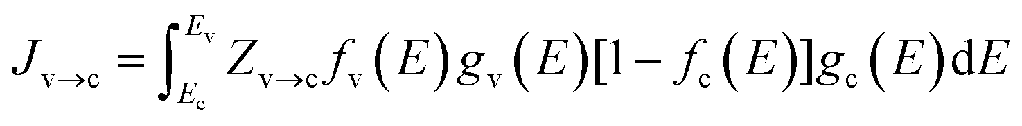
The RJ physically and electrically connects the subcells in a 2-T tandem and is the location where the charge carriers (i.e. electrons/holes) collected from the rear of the (n–i–p/p–i–n) top cell recombine with the charge carriers (holes/electrons) collected from the front of the bottom cell.17 Quantum-mechanical tunneling of electrons through classically forbidden regions into empty states physically enables this majority-carrier recombination process.18 In this article we often refer to collected carriers as majority carriers, following terminology from c-Si PV. In the context of semiconductors, interband tunneling was discovered by Esaki, investigating degenerately doped p–n homojunctions in germanium.19Fig. 1a and b respectively show the typical “S” shaped J–V characteristic (in the dark) and the associated band diagrams at different working points of such a tunnel diode. Both p- and n-sides are degenerately doped (with dopant concentrations of approximately 1019 cm−3); in this structure, the Fermi level, EF, effectively lies energetically below the VBMp and above the CBMn, respectively [VBMp and CBMn are the valence band maximum and conduction band minimum of the Ge(p+) and Ge(n+) regions, respectively]. We follow Esaki's reasoning to explain heuristically the operation of a tunnel diode in the dark. At zero-voltage bias (Vx = 0 V), the field-emission current density Jv→c (corresponding to electrons injected from VBp into the empty states of CBn), and the diffusion-driven current density Jc→v (corresponding to electrons injected from CBn into the empty states of VBp) should be balanced, with the following associated expressions: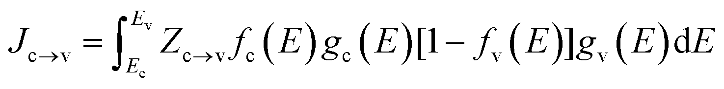 | (1) |
 | (2) |
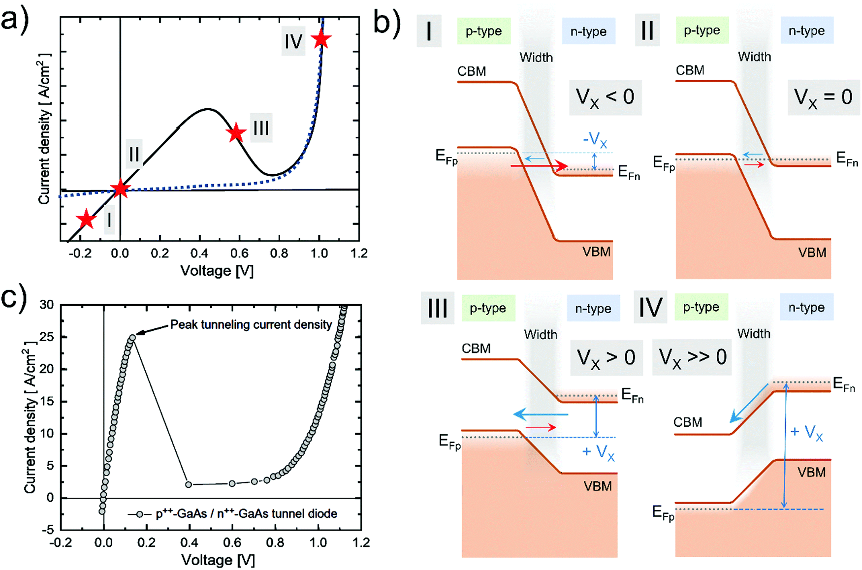 | ||
| Fig. 1 (a) J–V characteristic of an ideal tunneling diode (full line) compared with a standard p–n diode (dashed). (b) Band diagram of the tunneling diode with degenerate doping of the p-type and n-type semiconductors, under different polarization conditions (I–IV). Red arrow: Electron field-emission current, blue arrow: electron diffusion current. Adapted from ref. 18. (c) Experimental J–V curve of a tunneling diode composed of a degenerate doped GaAs junction. Panel (b) adapted from ref. 20. | ||
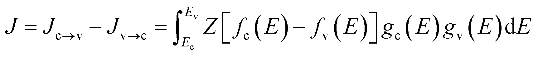
In this, Zc→v and Zv→c are the probabilities for electrons to tunnel through the bandgap from either side of the device (approximatively identical, Z), fc(E) and fv(E) are the Fermi–Dirac distributions; gc(E) and gv(E) the density of states for the electrons in the respective bands. It follows that increased doping on both sides will increase both electron diffusion and field emission by interband tunneling, and therefore increase the associated current densities Jc→v and Jv→c. However, both current densities are in equilibrium at zero bias, so no net-current flows [working point (II) in Fig. 1] and, evidently, EF is aligned on both sides.
When the junction is slightly voltage biased, Esaki argued that the net current density becomes
 | (3) |
Under reverse bias (Vx < 0 V), Jv→c starts to dominate over Jc→v, resulting in a net electron flow to the Ge(n+) side. Conversely, when a small forward bias (Vx > 0 V) is applied, Jc→v dominates over Jv→c resulting in a net electron flow to the Ge(p+) side. For even larger positive bias (Vx ≫ 0 V), the two bands become energetically misaligned, resulting in a reduced tunneling effect and therefore a drastic decrease of Jc→v. In this condition, the junction starts behaving like a standard diode (carrier transport happens now within the same band) with its expected exponential scaling of the current with applied bias (J–V).
In the case of a RJ embedded in a tandem solar cell, no voltage bias is applied across the RJ. However, under illumination, the p+ and n+ sides of the RJ encounter a continuous supply of electrons and holes respectively from their associated subcells, which annihilate each other through interband recombination. Also, in the tandem case, to maximize the generated voltage the electron and hole populations on either side of the RJ should be as much as possible on similar energetic levels, so that carrier recombination across the RJ does not result in significant voltage losses.
The Esaki diode represents an ideal model for the RJ, entirely relying on interband tunneling. Multi-junction tandems based on III–V semiconductors often include Esaki-type RJs, as III–V semiconductors often satisfy the condition of degenerate doping with atomically sharp junctions, obtained through epitaxial growth, using high-vacuum deposition techniques.20–22Fig. 1c shows the experimental J–V curve of an isolated GaAs(p++)/GaAs(n++) junction,20 showing qualitatively the same characteristics as Esaki's historical tunneling diode. However, the multi-layer configuration of tandem solar cells complicates the study of the isolated electrical properties of their RJ.
Experimentally, in perovskite-based tandem solar cells, the RJ is usually not an ideal Esaki-type tunneling diode. Indeed, the RJ is often a heterojunction (or hybrid junction) rather than a homojunction, where we classify heterojunctions as consisting of two semiconductors with different bandgaps, and hybrid junctions as consisting of two different materials classes, such as organic and inorganic semiconductors and metal oxides. Moreover, in the heterojunction or hybrid junction case, EF may lie within the materials’ bandgap; it may even be that n-type materials (but with a very high workfunction) are employed on the hole-collecting side.
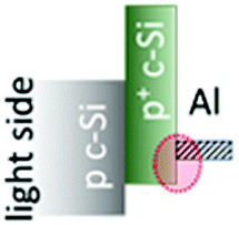
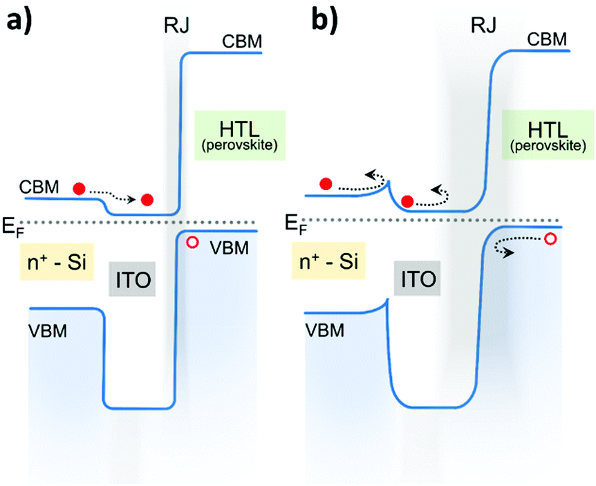
In practical tandems, the two layers that make up the RJ are often simply the electron and hole transport layers (ETL and HTL) of the respective subcells,23,24 thereby fulfilling a dual role: collecting carriers from one of the subcells and enabling efficient majority-carrier recombination through the RJ they form when stacked. In the case of c-Si bottom cells, the RJ layer will depend on the employed c-Si cell technology, which can be divided in two categories based on their charge-collecting regions at the front: (i) a dopant-diffused region of the c-Si wafer when employing standard c-Si solar cell technology [e.g. so-called Al back surface field (BSF) or passivated emitter and rear cells (PERC)] (ii) a deposited doped-silicon thin film [either hydrogenated amorphous silicon (a-Si) or nano-crystalline silicon (nc-Si)], when using silicon heterojunction (SHJ) or poly-Si contact technology.13 In the latter cases, usually a thin intrinsic buffer layer (usually either intrinsic a-Si or SiOx, respectively) is present between doped-silicon thin film and c-Si substrate, to aid in surface passivation. We note here that SHJ solar cells employ so-called passivating contacts on both sides of the device, enabling record-high operating voltages.25 Moreover, with well-designed transparent electrodes (usually transparent conductive oxides, TCOs) at their front and rear, SHJ cells feature high external quantum efficiencies (EQEs) for long-wavelength photons, thanks to their displaced-metal rear contact structure and the possibility to employ dopant-free junctions.26 For these reasons, they may be regarded as ideal bottom cell partner in silicon-based tandems,27 and have indeed been employed for most high-efficiency perovskite/silicon tandems to date. According to the polarity of the tandem, these silicon films can – at least in principle – be coupled either as Si(n+) with the perovskite HTL or as Si(p+) with the perovskite ETL, resulting respectively in Si(n+)/HTL and Si(p+)/ETL hybrid RJs. In this text, we labelled all RJs following the deposition order of the layers: from bottom cell to top cell for silicon/perovskite and CIGS/perovskite tandems (as these devices are built in the substrate configuration; the perovskite is at the sunward side), and from the top cell to the bottom cell for all-perovskite tandems (as these devices are built in the superstrate configuration onto glass, the latter facing the sun). Fig. 2a and b show the band diagrams of the RJ in silicon/perovskite tandems for both polarities, assuming that the HTLs and ETLs are ‘genuinely’ p-type and n-type, respectively (i.e. having their EF close to their VBM and CBM respectively).
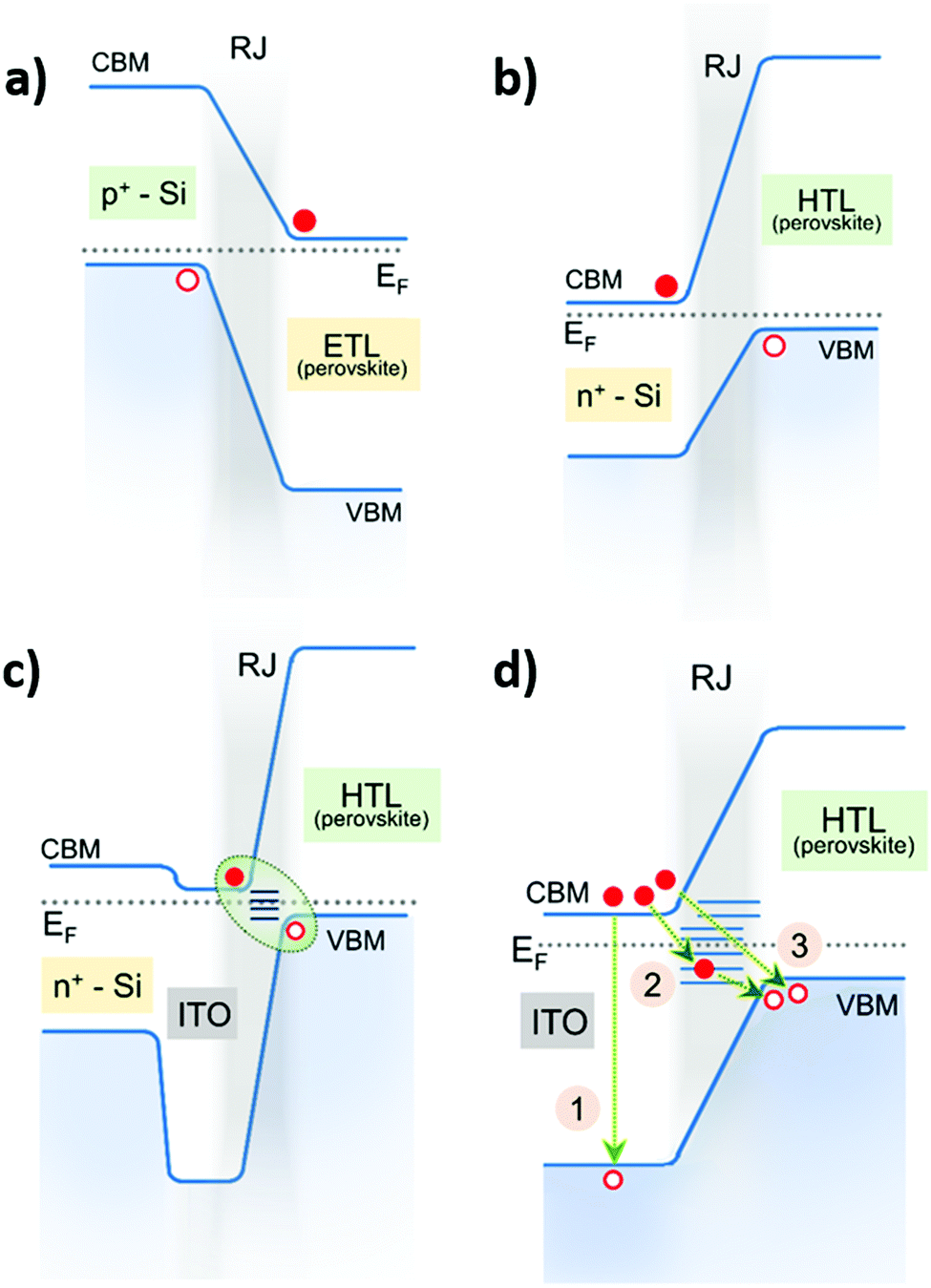 | ||
| Fig. 2 Band diagrams of the RJ in silicon/perovskite tandems. (a) and (b) General cases of p–i–n and n–i–p tandems based on the perovskite top cell configuration. (c) Band diagram of the ITO-assisted RJ. (d) Zoom-in of panel c that represents the recombination mechanisms at the ITO/perovskite HTL interface for a p–i–n tandem. | ||
Practically, exploiting the fact that often the dopant-type of deposited silicon films can be changed during film deposition, especially when using plasma-deposition processes, it is also possible to fabricate the RJ in situ during c-Si cell fabrication, by depositing Si(n+)/Si(p+) or Si(p+)/Si(n+) homojunction stacks, depending on the desired polarity.28–30 When heavily doped, these stacks resemble ideal Esaki diodes. Earlier, for c-Si cells, such doped-Si stacks already found application in interdigitated back-contact SHJ cells that featured tunnel-junction based ETLs.31 Even before that, such homojunctions were commonly employed in so-called micromorph thin-film tandems, which stacked a wider bandgap a-Si cell onto a micro/nano-crystalline bottom cell.32 In silicon/perovskite tandems, on top of such a homojunction RJ, one could then directly deposit the relevant charge transport layers of the perovskite top cell [i.e. Si(n+)/Si(p+)/HTL or Si(p+)/Si(n+)/ETL]. The latter configuration was already successfully implemented in silicon/perovskite tandems, firstly by Mailoa et al. and later by Shali et al.33,34 Notably, such doped Si-based layers can be optically tuned towards lower refractive indices by depositing e.g. SiOx-based films; having a RJ with its refractive index in between those of the perovskite and silicon cells aids in effective light coupling into the tandem.35,36 We also note here that passivating-contact c-Si solar cells in research laboratories increasingly feature so-called ‘dopant-free’ charge-selective layers, replacing the doped Si layers, often by metal oxides. Here, the main motivation is to reduce parasitic optical absorption in the front stacks of single-junction c-Si solar cells.25 A prominent example is to replace the Si(p+) film with high workfunction HTLs, such as MoOx, which have proven to lead to high single-junction device performance.37 Alternative HTL materials for the c-Si subcell can be VOx, WOx CuOx, and CuSCN;38–40 NiOx is also a potential candidate, but interfacing NiOx with c-Si remains challenging; doping the NiOx may potentially resolve this issue.41 The transition metal oxides MoOx, VOx, and WOx are particularly interesting: due to their high workfunction, they act as effective HTLs for c-Si solar cells. However, as they are n-type, the collected holes at the c-Si interface will recombine with the electrons of the n-type MoOxvia interband tunneling at the c-Si/MoOx interface. Therefore, these HTLs intrinsically introduce a RJ when deposited onto c-Si, with its recombination interface at the c-Si/MoOx interface. In the context of monolithic tandems, it may be beneficial to retain such materials, as they could directly be implemented as RJs. Onto the MoOx, one can then directly deposit the ETL of the top cell, as already proved in organic-PV tandems.42 In this case, it is the bottom-cell absorber/HTL interface that forms the RJ, not the HTL/ETL stack.
In the case of hybrid RJs, achieving degenerate doping in both constituents of the RJ is often not possible, especially when one of the layers is the perovskite's HTL or ETL. In such a case, depending on the energy alignment, majority carrier recombination at the RJ interface should be enhanced to avoid excessive resistive losses, which may be possible through trap-assisted tunneling (TAT).43,44 In TAT, the carriers tunnel into trap states, situated at the RJ interface between the two subcells.45 Energetically, this process is similar to Shockley–Read–Hall (SRH) trap-assisted recombination, even though all carriers involved are majority carriers collected from the respective subcells (rather than one minority and one majority carrier in the classic SRH case), which then recombine via sub-bandgap states at the interface. Strategies to enhance this mechanism involve inserting ultrathin metal layers within the RJ, or inserting a non-metal layer between the respective charge transport layers to aid in the recombination process.42,46 In single-junction SHJ cells, indium tin oxide (ITO), or a comparable TCO, is often used as a transparent top electrode, forming a low-resistive contact with the doped-silicon charge transport layers underneath.47 In the case of tandems, it might be beneficial to retain this TCO as part of the RJ, as it is usually a degenerately-doped n-type material, whose workfunction can be tuned to lower values (Fig. 2c). Therefore, this TCO layer can actually be employed as the n+-type region of the RJ. The role of the p+-type region in the RJ can then be fulfilled by the HTL of the top or bottom cell, depending on the tandem polarity. To avoid undesired parasitic absorption of long-wavelength photons due to free-carrier absorption (FCA) in the TCO, its thickness must be kept to a minimum. Moreover, with the possibility of PSCs featuring pinholes, it may be critical to keep the sheet resistivity of the TCO high (while maintaining its workfunction low), else the device can become shunted.48,49
The polarity of the RJ is governed by the tandem cell polarity, which at present is mainly dictated by the broadband transparency of the sunward contact stacks of the perovskite subcell. For this reason, at present, the p–i–n configuration (i.e., the ETL side is sunward) is preferred over its n–i–p counterpart in silicon/perovskite tandems.50 Indeed, to date, only a few highly-transparent HTLs have been developed for PSCs.51 As a consequence, the most frequently reported RJ is based on the p–i–n top cell structure, implying a Si(n+)/ITO/HTL structure between top and bottom cells. At the ITO/HTL RJ interface, the charges may recombine in principle via three different mechanisms (Fig. 2d).20 Direct tunneling (1) rarely occurs due to unfavorable band alignment (due to non-degenerate doping on the HTL side). Fortunately, the interface is usually quite defective, allowing for TAT (2) via interfacial trap states between the ITO and the HTL to be the dominant recombination pathway. However, we note here that the presence of interface states can also lead to Fermi-level pinning (FLP), with associated induced Schottky barriers; in case of insufficient workfunction differences between the RJ materials; the width of such barriers may prevent effective carrier transport. Employing interfacial materials with large workfunction differences can reduce these barriers, enabling effective carrier transport. We discuss this phenomenon in further detail below. Finally, in theory, ‘local’ tunneling where electron/holes recombine at the same position is a possibility (3);20 however, the mechanism is a rarity for wide-bandgap materials and is undesired due to the associated voltage losses.
Notably, the described TCO/HTL RJ structure closely resembles the ‘standard’ anode (i.e. hole collecting) contact stack of a variety of single-junction solar cells. Indeed, most – if not all – anode contact stacks of single-junction solar cells inherently feature a RJ, the underlying reason being that, without a bandgap, the outer metal electrodes only conduct electrons, not holes. A list of examples of currently employed anode contacts, which may serve as templates for new RJs, are summarized in Table 1 for both c-Si and perovskite single-junction solar cells where the red circle indicates the physical location of the RJ (note again the particular case of MoOx, where the RJ is situated at the interface shared with the silicon, rather than that with ITO). In general, a tandem-RJ should feature all the typical characteristics associated with a good contact: minimal minority-carrier recombination with low resistive losses.52 Minority-carrier recombination leads to voltage and charge-extraction losses, which can be mitigated through effective contact-passivation strategies.52 From the majority-carrier point of view, the contact resistivity (ρc) is of particular importance for the interfacial structures, representing the resistive losses experienced by majority carriers when transported from the semiconductor to the external electrode of single-junction devices. Its value is determined by the combined interface and bulk resistances of the contact materials to the collected charges. The bulk contributions can be usually neglected as the involved layers are very thin; interfacial transport typically dominates ρc, which is also the case for RJs. In addition to these criteria, as stated earlier, to maintain high tandem voltages, it is also important to minimize voltage losses across the RJ by workfunction engineering.
| Solar Cells | RJ | Energy diagrams |
|---|---|---|
| Perovskite n–i–p | Spiro/Au |
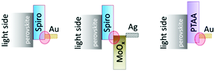
|
| Spiro/MoOx/Ag | ||
| PTAA/Au | ||
| Perovskite p–i–n | NiOx/ITO |
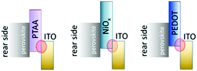
|
| PTAA/ITO | ||
| PEDOT/ITO | ||
| Silicon heterojunction | a-Si(p+)/TCO |
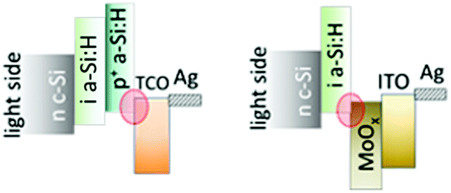
|
| a-Si(i)/MoOx/ITO | ||
| Silicon homojunction | c-Si(p+)/Al |
|
For single-junction solar cells, an excessive amount of defect states may be present at each of the interfaces of the contact stacks. At the interfaces shared with the photovoltaic absorbers, from a minority-carrier perspective, such defect states lead to voltage losses through trap-assisted (SRH) recombination, mandating effective surface passivation strategies. From a majority-carrier perspective, these states can also result in FLP, which may lead to the presence of transport barriers at the interfaces, impairing the charge-selectivity of the contacts. Indeed, FLP results in a deviation of the predicted energetic barrier that forms at contacts from the Schottky–Mott theory (in which the barrier height is defined by the difference between the workfunction of the contact material and the electron affinity of the semiconductor). Now, by considering the analogies drawn before between the solar cell contacts and the RJ, it is evident that the RJ can be affected by FLP as well (Fig. 3a). In silicon, for example, FLP is a significant impediment in forming carrier-selective contacts via direct metallization, owing to the presence of a high concentration of surface defects (silicon dangling bonds), as well as metal-induced gap states.53 These defect- and metal-induced gap states (DIGS and MIGS) limit the ability of the overlying metal workfunction to manipulate the surface potential of c-Si, impairing charge-selectivity (Fig. 3b). Interfacial dipoles, resulting from the newly formed Si-metal bonds, are also argued to contribute to FLP.54 To overcome FLP, either the c-Si subsurface has to be heavily doped to narrow the barrier width and enable intraband tunneling through the Schottky barrier (these are classic Ohmic contacts, used e.g. in Al-BSF and PERC c-Si technologies), or so-called passivating contacts, which simultaneously passivate surface defects and displace the metal electrode from the interface have to be realized. We remark that interband tunneling involves carrier tunneling to different bands; for intraband tunneling, the carrier remains in the same band.25
 | ||
| Fig. 3 Band diagram of the RJs of the silicon/perovskite tandems with (a) ideal and (b) with Fermi level pinned contacts. | ||
Lessons can be learned from these passivating-contact architectures for the design and implementation of effective tunnel junctions, where ETLs and HTLs of the subcells directly interface with one another. If this interface is indeed suffering from FLP, it may not be possible to lower the height of the induced transport barriers. However, through workfunction engineering on both sides of the RJ, possibly through doping strategies, it may be possible to narrow the barrier widths; in such a case, doping simultaneously enhances intraband as well as interband tunneling. However, doping-related FCA of longer-wavelength photons may be a possible detrimental side effect, leading to optical losses in the tandem.
Practical implementation of recombination junctions in silicon/perovskite tandems
The materials selection for RJs are dictated – besides the tandem polarity – by the characteristics of the bottom and top cells. Fig. 4 summarizes the main configurations of RJs for silicon/perovskite tandems reported to date. We divided the RJs in two groups, based on the type of silicon bottom cell: RJs in passivating-contact bottom cells, and RJs in diffused-contact bottom cells.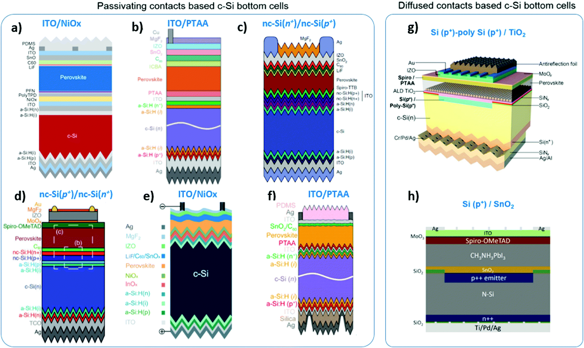 | ||
| Fig. 4 Representative examples of the successful RJs used in literature for passivating contacts and diffused-junction contacts based c-Si bottom cells (References: a,55 b,56 c,49 d,33 e,57 f,58 g,59 h60 reprint with permissions). | ||
Passivating-contact silicon bottom cells
In this group, most of the RJs include a TCO layer such as ITO, IZO, ZTO. In many single-junction passivating-contact silicon devices TCOs are an inherent part of the front-contact stack and have thus already been well optimized to yield also a low ρc with the silicon charge transport layer. As stated, TCOs have the benefit to control the carrier concentration, the energy level, and can thus also be good partners in a RJ as the n+-layer. In addition, TCOs usually provide a low ρc with most perovskite charge transport layers. Therefore, retaining TCOs in the tandem structure has the advantage of fairly straightforward tandem integration of top and bottom cells, utilizing already established HTLs and ETLs for PSCs.In the p–i–n configuration, tandems, built onto front-flat silicon bottom cells have shown excellent performances when using RJs based on ITO/NiOx (Fig. 4a) and ITO/PTAA (Fig. 4b).23,55,56,61,62 However, as already stated, the lateral conductive character of the TCO as part of the RJ may promote shunting through the top cell, resulting in a low VOC and FF, in those cases where the top cell would feature pinholes. This is of specific concern for PSCs built onto macroscopically rough substrates, such as tandems based on textured c-Si bottom cells, and when solution processing is used for the perovskite deposition. We note that textured tandems are closer to industrial manufacturing compared to their front-flat counterparts, underlining the importance of developing strategies towards shunt-free tandems through RJ and perovskite engineering. Moreover, a low lateral conductivity of the RJ is also likely to be essential for the scaling up of any type of perovskite-based tandem solar cell, since even small local shunts cause a drastic decrease in the shunt resistivity of the device.33 To overcome this shunting issue, Sahli et al. avoided the use of a TCO, and introduced nc-Si(n+)/nc-Si(p+) RJs, onto which then the perovskite-HTL was deposited. This structure enables a low lateral conductivity, however, the interface between nc-Si(p+) and typical metal oxide-based HTLs as used in single-junction PSC development, such as NiOx, may suffer from a high ρc.63 To this end, Sahli et al. utilized evaporated spiro-TTB as a dopant-free small molecule HTL, resulting in the combination of a low lateral conductivity and a lower ρc (Fig. 4c).49 Nevertheless, finding non-soluble HTLs based on organic materials, compatible with such nc-Si RJs remains an open challenge. We note that with a similar approach Sahli et al. also explored RJs with the opposite polarity, based on nc-Si(p+)/nc-Si(n+) as a RJ, onto which C60 was then evaporated as the perovskite-ETL (only on front-flat bottom cells, to date, Fig. 4d).33 Another pathway to mitigate shunts induced by the textured c-Si bottom cell, was proposed Hou et al. and Chen et al.58,64 In these works, the perovskite film, deposited on textured-silicon bottom cells by spin-coating (Fig. 4e) or blade-coating (Fig. 4f), was drastically increased in thickness, eliminating the chance of having pinholes or punching-through of the perovskite by the texturing, resulting in a reduction of shunt paths. Such an innovation is important since it allows for the use of RJs based on established materials such as TCOs and perovskite ETLs and HTLs, even on textured bottom cells, and does not require the very long plasma-depositions needed to grow the nc-Si(p+)/nc-Si(n+) stacks.
We also highlight here how the optical properties of the RJ play as well an important role in the near-infrared response of the bottom cells.65 As already stated, highly doped TCOs contribute to high parasitic absorption in the near-infrared region due to FCA, resulting in reduced photocurrent from the bottom cell.47 Moreover, FCA results in undesired device heating, leading to performance losses and a shortened time-to-failure of commercial products. To overcome this issue, similar as for the front-contact TCO, a high carrier mobility TCO with high infrared transparency, such as H-doped In2O3, or Zr-doped In2O3 can be utilized.66,67 In addition, matching the optical properties of all layers that comprise the RJ with those of the tandem, especially in terms of their refractive indices and layer thicknesses, can be similarly effective in improving light absorption in the tandem semiconductors. In this context, Mazzarella et al. employed a RJ layer stack of nc-SiOx, which combines the advantages of the nc-Si based RJs (negligible parasitic absorption for wavelengths >600 nm) with a refractive index between that of the perovskite and silicon, which minimizes the reflection losses. These optical properties resulted in an increase of the overall JSC of tandem solar cells with a polished front Si surface.35
Diffused-junction silicon bottom cells
In their single-junction implementation, such diffused-junction silicon solar cells usually do not require TCOs (Fig. 4g and h), as the lateral conductivity of the diffused regions is usually sufficiently high to transport charge carriers to the front metal grid. In the tandem cell, the current flow is in 1 dimension, so lateral charge transport is not required (as for nc-Si(Ox) recombination junctions). Therefore, materials providing a low ρc and efficient charge selectivity, directly deposited onto these diffused regions, are good candidates to form RJs.25 We remark here that single-junction diffused-junction silicon solar cells usually will feature a dielectric layer as anti-reflective coating, which in tandem implementations may be avoided due to its insulating character. Fig. 4 shows the examples of Si(p+)/poly-Si(p+)/TiO2 (Fig. 4g) and Si(p+)/SnO2 (Fig. 4h), where TiO2 and SnO2 are serving as both ETL and as a part of the RJ. In the former contact structure, the dopant tail from in-diffusion from the poly-Si into the c-Si acts as a shallow diffused junction.Silicon/perovskite tandem performance: impact of the recombination junction
We now briefly revisit the different RJs, but focus on the performance of the different proposed tandems and classify them from a RJ point of view (Fig. 5). In the literature, front-side polished tandems are still more common, since the flat surface enables simpler solution processing of the perovskite. The earliest RJ designs featured a TCO as central part of their RJ. An example of this RJ being a TCO/NiOx stack (Fig. 5, RJ-A). However, these tandems suffered from a relatively low VOC, with values around 1.65 eV.23,68 This could largely be attributed to interfacial defects at the NiOx/perovskite interface that act as recombination centers, which significantly reduced the VOC of the top cells.69 When the NiOx surface was modified with poly-TPD and PFN, the VOC improved significantly; similar improvements were obtained by replacing the NiOx altogether with PTAA.55,56,70,71 Conversely, when the TCO-based RJ stack is inverted to a-Si(p+)/TCO (Fig. 5, RJ-B), the tandem PCEs were limited by parasitic absorption in the hole-collecting top contact of the perovskite sub-cell (JSC < 17 mA cm−2) and the PCEs remained below 23%.61,72,73 Once more, this highlights the importance of light management in tandem devices, not only by tuning the absorber bandgaps adequately but also through consideration of all of the other layers comprising the device.74 In addition to parasitic losses, reflection losses also need to be carefully considered. For this reason, the tandems incorporating nc-SiOx underneath TCO/HTL RJs (Fig. 5, RJ-C) were proven to be highly advantageous for application on planar Si sub-cells, with a gain in JSC of ∼1.5 mA cm−2 as compared to their non-oxide counterparts (RJ-A).35,75 Consequently, RJ-C enhanced the JSC above 19 mA cm−2, resulting in a certified PCE of 25.4%.35 Conversely, the n–i–p configuration employing nc-SiOx underneath the TCO/ETL RJ (Fig. 5, RJ-D) did not yield the same benefit in current enhancement, again due to the additional parasitic losses originating from the hole-collecting top contact.76 As discussed, for TCO-free RJs, Sahli et al. first tested the n–i–p configuration using nc-Si(p+)/nc-Si(n+) RJs (Fig. 5, RJ-E).33 However, similar to RJ-D, the problem of parasitic absorption in the hole-collecting top contact overshadowed the benefits of this RJ, such that the JSC and PCE remained below 17 mA cm−2 and 23%, respectively. This TCO-free RJ was proved to be more successful in the p–i–n configuration, using nc-Si(n+)/nc-Si(p+) on textured-silicon bottom cells (Fig. 5, RJ-F),49 resulting in a JSC of 19.5 mA cm−2 and a certified PCE of 25.2%. A different type of fully textured tandem design incorporating a p-type crystalline silicon bottom cell with a silicon carbide based RJ layer, nc-SiCx(n+)/nc-Si(p+) (Fig. 5, RJ-G), was also proven to deliver a PCE of 25.1% with a JSC of 19.5 mA cm−2.77 Among the RJs on diffused-junction bottom cells, poly-Si(p+)/ETL (Fig. 5, RJ-H) and Si(p+)/ETL (Fig. 5, RJ-K) are two examples.59,60,78 Other types of diffused-junction Si-based tandem devices were also reported, where the doped-Si and ETL or HTLs were stacked together via an intermediate TCO layer, such as Si(n+)/TCO/HTL (Fig. 5, RJ-I) and Si(p+)/TCO/ETL (Fig. 5, RJ-J). In these tandem designs, the main motivation for using a diffused-junction c-Si bottom cell stems from its contemporary market dominance.79,80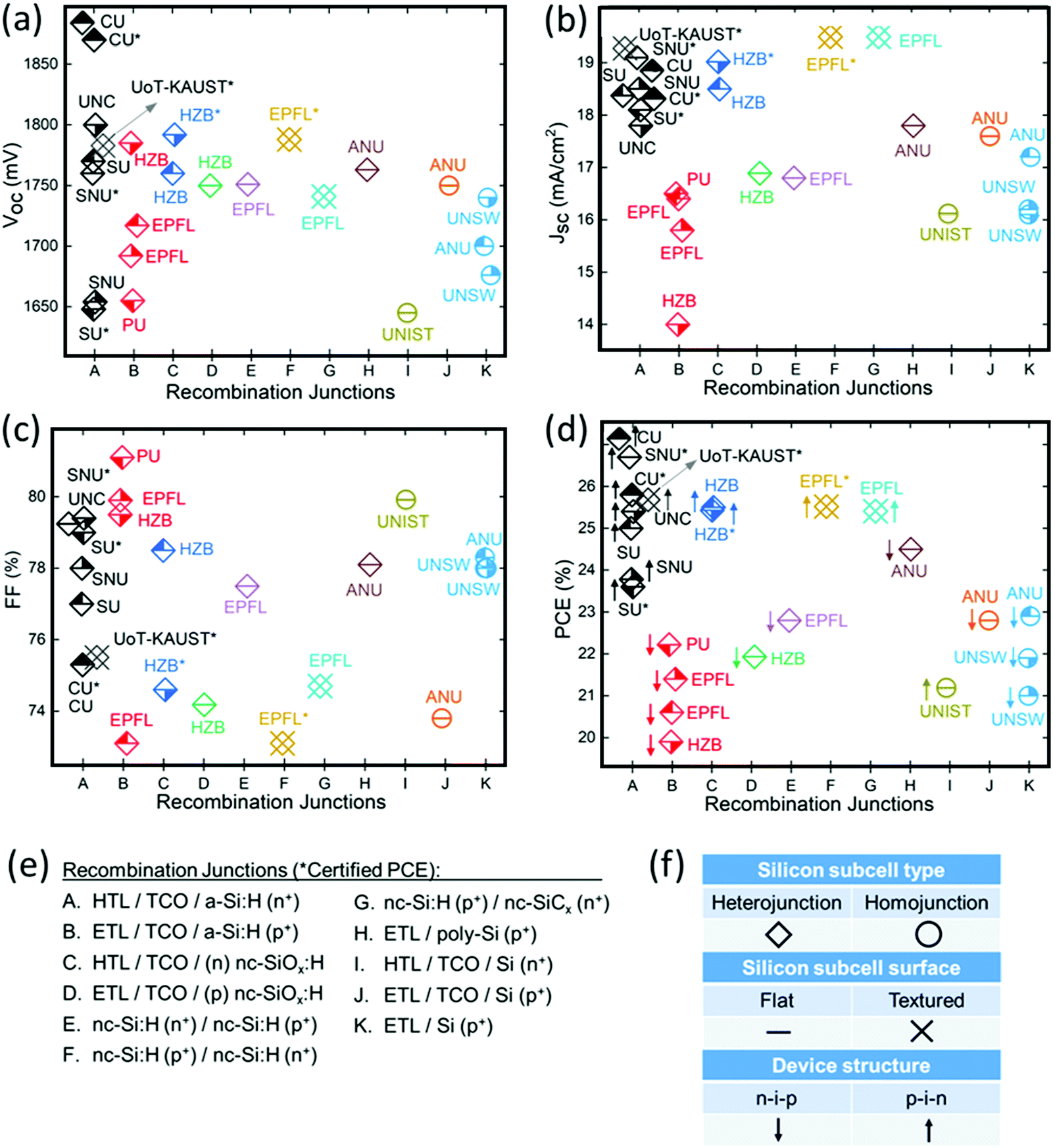 | ||
| Fig. 5 (a) VOC, (b) JSC, (c) FF and (d) PCE values of the reported silicon/perovskite monolithic tandem solar cells with different RJs. Descriptions for the RJs (e) and tandem device indicators (f). The asterisks represent independently certified values. | ||
As shown in Fig. 5, currently the most efficient tandem devices incorporate flat or textured passivating-contact bottom cells, connected to the top perovskite cells via a-Si(n+)/TCO/HTL, nc-SiOx(n+)/TCO/HTL, nc-Si(n+)/nc-Si(p+) or nc-SiCx(n+)/nc-Si(p+) RJs. Among the different bottom cell technologies, SHJ bottom cells are most suitable for reaching higher tandem PCEs, as already stated; also among single-junction c-Si PV, this technology holds the world record.81 Overall, so far, the fully textured design with TCO-free RJs incorporating nc-SiOx or nc-Si provide superior light management, and consequently, higher JSCs. Nonetheless, the FF values of all fully-textured design so far remain below 80%, most probably due to the electronic quality of the perovskite absorbers. Thus, addressing the FF issue of the fully-textured tandems will unlock the true potential of these devices, with PCEs expected to exceed 30%.
Another crucial parameter is the tandem VOC. The perovskite absorbers used for the most efficient tandem devices have a bandgap in between 1.63–1.70 eV.35,49,56 Arguably, any ‘high-quality’ PSC should have a VOC deficit (defined as Eg/q − VOC) of <0.4 V,10,52,82 implying that well-performing perovskites with a 1.64 eV bandgap should deliver on the device level a VOC of ∼1.24 V. When this is combined with a spectrally-filtered SHJ bottom cell's VOC of ∼0.7 V,49 achieving tandem VOC values >1.9 V is a reasonable target. However, as shown in Fig. 5a, the reported tandem VOC values to date are at least ∼0.15 V below this estimation. To minimize these VOC losses, a suitable RJ design is of high importance, of which the key properties should be well-passivated interfaces, carrier populations on both sides of the RJ at similar energetic positions, a low ρc, as well as negligible parasitic absorption and reflection losses. Later, we discuss several strategies to quantify the VOC losses originating from the RJ layers (Tables 2 and 3).
| RJ | Surface | Silicon | V OC (V) | J SC (mA cm−2) | FF (%) | PCE (%) | Ref. | |
|---|---|---|---|---|---|---|---|---|
| The asterisks indicate independently certified results. | ||||||||
| A | HTL/TCO/a-Si:H (n+) | Flat | Heterojunction | 1.76 | 19.1 | 79.2 | 26.7* | 71 |
| Flat | Heterojunction | 1.89 | 19.12 | 75.3 | 27.1 | 55 | ||
| Flat | Heterojunction | 1.87 | 18.3 | 75.3 | 25.8* | 55 | ||
| Textured | Heterojunction | 1.78 | 19.2 | 75.4 | 25.7* | 57 | ||
| Flat | Heterojunction | 1.80 | 17.8 | 79.4 | 25.4 | 56 | ||
| Flat | Heterojunction | 1.77 | 18.4 | 77.0 | 25.0 | 70 | ||
| Flat | Heterojunction | 1.65 | 18.5 | 78.0 | 23.8 | 68 | ||
| Flat | Heterojunction | 1.65 | 18.1 | 79.0 | 23.6 | 23 | ||
| B | ETL/TCO/a-Si:H (p+) | Flat | Heterojunction | 1.65 | 16.5 | 81.1 | 22.2 | 73 |
| Flat | Heterojunction | 1.69 | 15.8 | 79.9 | 21.4 | 61 | ||
| Flat | Heterojunction | 1.72 | 16.4 | 73.1 | 20.6 | 83 | ||
| Flat | Heterojunction | 1.78 | 14.0 | 79.5 | 19.9 | 80 | ||
| C | HTL/TCO/(n) nc-SiOx:H | Flat | Heterojunction | 1.76 | 18.5 | 78.5 | 25.5 | 75 |
| Flat | Heterojunction | 1.79 | 19.0 | 74.6 | 25.4 | 35 | ||
| D | ETL/TCO/(p) nc-SiOx | Flat | Heterojunction | 1.75 | 16.9 | 74.2 | 21.9 | 76 |
| E | nc-Si:H (n+)/nc-Si:H (np+) | Flat | Heterojunction | 1.75 | 16.8 | 77.5 | 22.8 | 33 |
| F | nc-Si:H (p+)/nc-Si:H (n+) | Textured | Heterojunction | 1.79 | 19.5 | 73.1 | 25.5 | 49 |
| G | nc-Si:H (p+)/nc-SiCx (n+) | Textured | Heterojunction | 1.74 | 19.5 | 74.7 | 25.4 | 77 |
| H | ETL/poly-Si (p+) | Flat | Heterojunction | 1.76 | 17.8 | 78.1 | 24.5 | 59 |
| I | HTL/TCO/Si (n+) | Flat | Homojunction | 1.64 | 16.1 | 79.9 | 21.2 | 79 |
| J | ETL/TCO/Si (p+) | Flat | Homojunction | 1.75 | 17.6 | 73.8 | 22.8 | 80 |
| K | ETL/Si (p+) | Flat | Homojunction | 1.70 | 17.2 | 78.3 | 22.9 | 59 |
| Flat | Homojunction | 1.74 | 16.2 | 78.0 | 21.9 | 60 | ||
| Flat | Homojunction | 1.67 | 16.1 | 78.0 | 21.0 | 78 | ||
| Bottom cell | Top cell | RJ | J SC mA cm−2 | V OC V | FF % | PCE % | Ref. |
|---|---|---|---|---|---|---|---|
| P3HT | ITO | P3HT/PCBM (sandwiched devices) | 8.4 | 1.95 | 66 | 10.8 | 84 |
| MAPbBr3 (2.2 eV) | PEDOT:PSS | (8.6) | (1.08) | (78) | (7.2) | ||
| c-TiO2 | MAPbI3 (1.55 eV) | (20.7) | (1.1) | (79) | (18) | ||
| FTO | PCBM | ||||||
| PTAA | ITO | PTAA/PCBM (sandwiched devices) | 8.3 | 2.25 | 61 | 10.4 | 84 |
| MAPbBr3 (2.2 eV) | PEDOT:PSS | (8.4) | (1.3) | (77) | (8.4) | ||
| c-TiO2 | MAPbI3 (1.55 eV) | (20.7) | (1.1) | (79) | (18) | ||
| FTO | PCBM | ||||||
| spiro-OMeTAD/PEDOT:PSS | hc-PEDOT:PSS electrode | PEDOT:PSS/PEI/PCBM/PEI | 6.61 | 1.89 | 56 | 7.0 | 85 |
| MAPbI3 (1.55 eV) | spiro-OMeTAD | (18.14) | (1.01) | (64) | (11.7) | ||
| c-TiO2/meso-TiO2 | MAPbI3 (1.55 eV) | (14.18) | (0.98) | (60) | (8.3) | ||
| FTO | PCBM:PEI | ||||||
| PCBM/SnO2/Zn:SnO2 | Ag | Zn:SnO2/ITO/PEDOT:PSS | 14.5 | 1.66 | 70 | 16.9 | 24 |
| FA0.83Cs0.13Pb(I0.5Br0.5)3 (1.8 eV) | C60/BCP | (15.1) | (1.12) | (58) | (9.8) | ||
| NiOX | FA0.75Cs0.25Sn0.5Pb0.5I3 (1.2 eV) | (26.7) | (0.74) | (71) | (14.1) | ||
| ITO | PEDOT:PSS | ||||||
| TaTm/TaTm:F6-TCNNQ | Au | TaTm:F6-TCNNQ/C60:PhIm | 9.83 | 2.294 | 80.3 | 18.1 | 86 |
| Cs0.15FA0.85Pb(I0.3Br0.7)3 (2 eV) | TaTm/TaTm:F6-TCNNQ | (11.4) | (1.20) | (77.8) | (10.7) | ||
| TiO2/IPH | MAPbI3 (1.55 eV) | (21.8) | (1.07) | (81.6) | (19.1) | ||
| ITO | C60:PhIm/C60 | ||||||
| C60/bis-C60 | Ag | bis-C60/ITO/PEDOT:PSS | 12.7 | 1.98 | 73 | 18.4 | 87 |
| MA0.9Cs0.1Pb(I0.6Br0.4)3 (1.8 eV) | IC60BA/bis-C60 | (15.1) | (1.2) | (69) | (12.5) | ||
| NiOX | MAPb0.5Sn0.5I3 (1.2 eV) | (25.5) | (0.84) | (67) | (14.4) | ||
| ITO | PEDOT:PSS | ||||||
| spiro-OMeTAD/PEDOT:PSS | Au | PEDOT:PSS/C60 | 6.40 | 1.96 | 41 | 5.1 | 88 |
| MAPbBr3 (2.3 eV) | spiro-OMeTAD | (6.16) | (1.41) | (64) | (5.2) | ||
| c-TiO2/meso-TiO2 | MAPbI3 (1.55 eV) | (17.7) | (1.04) | (71) | (12.7) | ||
| FTO | C60 | ||||||
| C60/ALD-SnO2 | Ag | ALD-SnO2/ITO/PEDOT:PSS | 14.8 | 1.81 | 70 | 19.1 | 89 |
| FA0.6Cs0.4Pb(Br0.3I0.7)3 (1.76eV) | C60/BCP | (15.8) | (1.14) | (78) | (14.5) | ||
| PTAA | FA0.75Cs0.25Sn0.5Pb0.5I3 (1.2 eV) | (27.6) | (0.76) | (74) | (15.6) | ||
| ITO | PEDOT:PSS | ||||||
| TaTm/TaTm:F6-TCNNQ | Au | TaTm:F6-TCNNQ/C60:PhIm | 9.84 | 2.3 | 79.6 | 18.02 | 90 |
| MAPbI3 (1.55 eV) | TaTm/TaTm:F6-TCNNQ | (12.5) | (1.19) | (81.5) | (12.2) | ||
| TiO2/C60 | MAPbI3 (1.55 eV) | (18.7) | (1.13) | (83.3) | (17.6) | ||
| ITO | C60:PhIm/C60 | ||||||
| PTAA (TPE-MN3: Mo(tfdCOCF3)3) | Ag | PTAA (TPE-MN3: Mo(tfdCOCF3)3)/HMB-PC61BM | 13.36 | 1.79 | 78.2 | 18.7 | 91 |
| MAPbI3 (1.55 eV) | PTAA (TPE-MN3: Mo(tfdCOCF3)3) | (22.2) | (1.03) | (80) | (18.3) | ||
| TiOx/PC61BM | MASn0.25Pb0.75I3 (1.26 eV) | (26.5) | (0.77) | (76) | (15.6) | ||
| ITO | HMB-PC61BM | ||||||
| FSIP/C60/BCP FA0.83Cs0.17Pb(Br1.5I1.5) (1.83 eV) | Ag | Cu/Au | 12.5 | 1.84 | 78 | 17.9 | 92 |
| NiOX | PS/C60/BCP | (14.8) | (1.16) | (72) | (12.3) | ||
| ITO | FA0.5MA0.5Sn0.5Pb0.5I3 (1.24 eV) | (27.2) | (0.75) | (67) | (13.6) | ||
| PEDOT:PSS | |||||||
| C60/BCP | Ag | Ag/MoOx/ITO | 14.1 | 1.922 | 78.1 | 21.0 | 93 |
| FA0.8Cs0.2Pb(I0.7Br0.3)3 (1.75 eV) | C60/BCP | (16.4) | (1.14) | (74.4) | (18.1) | ||
| PTAA | (FASnI3)0.6(MAPbI3)0.4:Cl (1.2 eV) | (29) | (0.84) | (74.5) | (14.0) | ||
| ITO | PEDOT:PSS | ||||||
| LiF/C60/PEIE | Ag | PEIE/AZO/IZO/PEDOT:PSS | 16.0 | 1.88 | 77 | 23.1 | 94 |
| DMA0.1FA0.6Cs0.3PbI2.4Br0.6 (1.7eV) | C60/BCP | (19.6) | (1.2) | (82) | (19.2) | ||
| poly-TPD/PFN-Br | FA0.75Cs0.25Sn0.5Pb0.5I3 (1.2 eV) | (31.7) | (0.69) | (76) | (16.5) | ||
| ITO | PEDOT:PSS | ||||||
| C60/ALD-SnO2 | Cu | ALD-SnO2/Au/PEDOT:PSS | 15.6 | 1.965 | 81.0 | 24.8 | 95 |
| FA0.8Cs0.2Pb(I0.6Br0.4)3 (1.77 eV) | C60/BCP | (17.0) | (1.22) | (79.7) | (16.5) | ||
| PTAA | MA0.3FA0.7Pb0.5Sn0.5I3 (1.22 eV) | (31.4) | (0.83) | (80.8) | (21.1) | ||
| ITO | PEDOT:PSS | ||||||
| C60/ALD-SnO2 | Cu | ALD-SnO2/ITO/PEDOT:PSS | 15.1 | 1.99 | 77 | 23 | 96 |
| FA0.6Cs0.4Pb(I0.65Br0.35)3 (1.8eV) | C60/BCP | (17.0) | (1.22) | (78) | (16.3) | ||
| PTAA | Cd:FA0.5MA0.45Cs0.05Pb0.5Sn0.5I3 (1.22 eV) | (30.2) | (0.85) | (79) | (20.3) | ||
| ITO | PEDOT:PSS/PTAA |
Recombination junctions in all-perovskite tandems
The tunability of the perovskite bandgap via compositional tuning (from 1.2 eV to 3 eV) has led to the recent explorations of the all-perovskite tandem architecture, which utilizes perovskite absorbers in both top and bottom cells.97–99 All-perovskite tandems offer some fabrication advantages since many layers can be deposited from solution, and, in principle, are suitable for high-throughput fabrication techniques. All-perovskite tandems can also be processed on flexible substrates for high power-to-weight ratio modules.100 Assuming perfect tuneability, the radiative efficiency limit of such tandems is also slightly higher than of silicon/perovskite tandems. Monolithic, all-perovskite tandems may simply employ an ETL/HTL interface as the RJ. Most of the ETL/HTL RJs in all-perovskite tandem devices have low lateral conductivity with high charge selectivity. Therefore, they can serve as an efficient RJ with a high shunt resistance. However, the RJ in 2-T all-perovskite tandem devices may also need to be a chemical barrier to process-induced damage of the top cell perovskite (in the superstrate configuration) against the solubility of the orthogonal solvents, as sketched in Fig. 6.98,101 Towards this purpose, it maybe beneficial to reintroduce a TCO as a part of the RJ, which can serve as a protective layer for the perovskite top cell.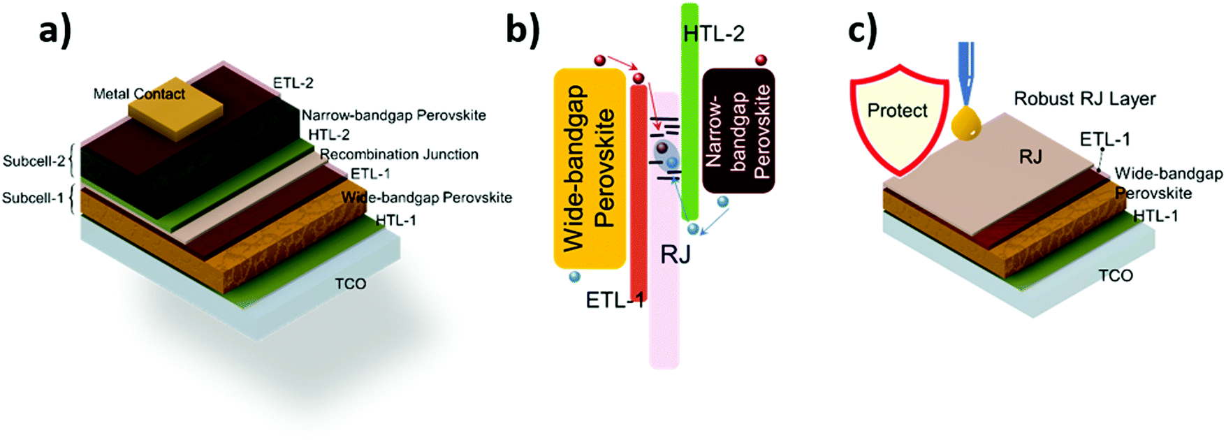 | ||
| Fig. 6 Schematic diagram illustrating the 2T-monolithic all-perovskite tandem structure (a), a sketch of the energy level diagram (b), and the functional role of RJs in these devices (c). | ||
The first example of a 2-T all-perovskite tandem device was reported by Heo et al. in 2016 via mechanically combining individual PSCs devices by stacking the P3HT with PCBM and PTAA with PCBM layers as the RJs.84 In that study, thinning down and introducing lithium and pyridine additives in the HTL enhanced the conductivity, enabling tandem devices with 2.25 V VOC and 10.4% PCE.84 As a step further, Sheng et al. employed organic semiconductors (PEDOT:PSS/C60) as the RJ in tandem devices wherein solution assisted fabrication of the top stack is realized. However, this resulted in a large VOC loss (∼0.5 V) with significant series resistance (and low FF) in the device.88 Following this strategy, Jiang et al., introduced a thin layer of PEI to form PEDOT:PSS–PEI/PCBM–PEI as the RJ.101 The PEI layer was reportedly introduced to create a workfunction contrast across the PEDOT:PSS film. The subsequent device stacks were fabricated using orthogonal solvents and film transfer lamination techniques, to ensure minimal dissolution of the layers underneath. Though the voltage losses are minimal here, significant resistive losses resulted in a low FF, leading to poor tandem devices in comparison to their subcells. In 2017 Forgács et al., followed in 2018 by Ávila et al., introduced vacuum-deposited, doped-small molecules of TaTm:F6-TCNNQ/C60:PhIm as a RJ and achieved 2.28 and 2.3 V VOC, respectively.86,90 Apart from the improved performance, importantly, the vacuum processing of the top cell eliminated the necessity of a protection layer, which is usually needed in solution processing. Chang et al. demonstrated that adding the cross-linking agent (1,2-bis[4-(azidomethyl) phenyl]-1,2-diphenylethene)(TPE-MN3) into the PTAA (bottom cell – HTL) layer increases the chemical robustness of the RJ.91 Furthermore, the addition of dopants to both the charge transport layers of the RJ [PTAA(TPE-MN3) with Mo(tfdCOCF3)3 and PC61BM with HMB] resulted in highly efficient tandems with sufficient chemical robustness to fabricate the top stack of the devices using solution processing techniques, without risk of subsequent dissolution.91 To summarize, most of the all-perovskite tandem studies utilizing organic ETL/HTL stacks report low PCE values due to the significant losses associated with low VOC and FF of these devices.84,86,88,90,91,101 Even though most of these charge transport layers have performed well in individual PSCs, the quality of their interfaces to serve as RJs and a protective barrier enabling top cell fabrication in tandem devices is lacking and needs further work.
As argued, utilizing a TCO as part of the RJ brings chemical robustness to the top/bottom perovskite device stack from damage during the fabrication of the bottom/top cell layers the superstrate/substrate configuration. However, TCOs are usually deposited by sputtering, which can result in plasma-induced damage of underlying soft layers. To overcome this, Eperon et al. introduced a thin stack of atomic layer deposited (ALD) SnO2/Zn:SnO2 as a buffer, minimizing damage to the device underneath from subsequent sputtering of ITO.24 Notably, for 2-T all-perovskite tandems, introducing TCOs such as ITO, IZO, and AZO as part of the RJ, also led to significant performance gains, especially in terms of FF, likely due to reduced resistive losses (Fig. 7).24,87,89,93,94,96 Recently, Yang et al. achieved 23%-efficient 2-T all-perovskite tandems (16.3% and 20.3% for the individual components) employing ALD-SnO2/ITO/PEDOT:PSS as the RJ with tandem voltage losses of only 80 mV compared to the sum of the individual subcells, and with a similar FF.57 Along similar lines, by introducing a low-temperature ALD-grown Al:ZnO layer in conjunction with sputtered IZO as interlayers, Palmstrom et al. demonstrated 23.1% efficient monolithic tandem devices, with a stabilized power output of 21.3% on flexible substrates.94
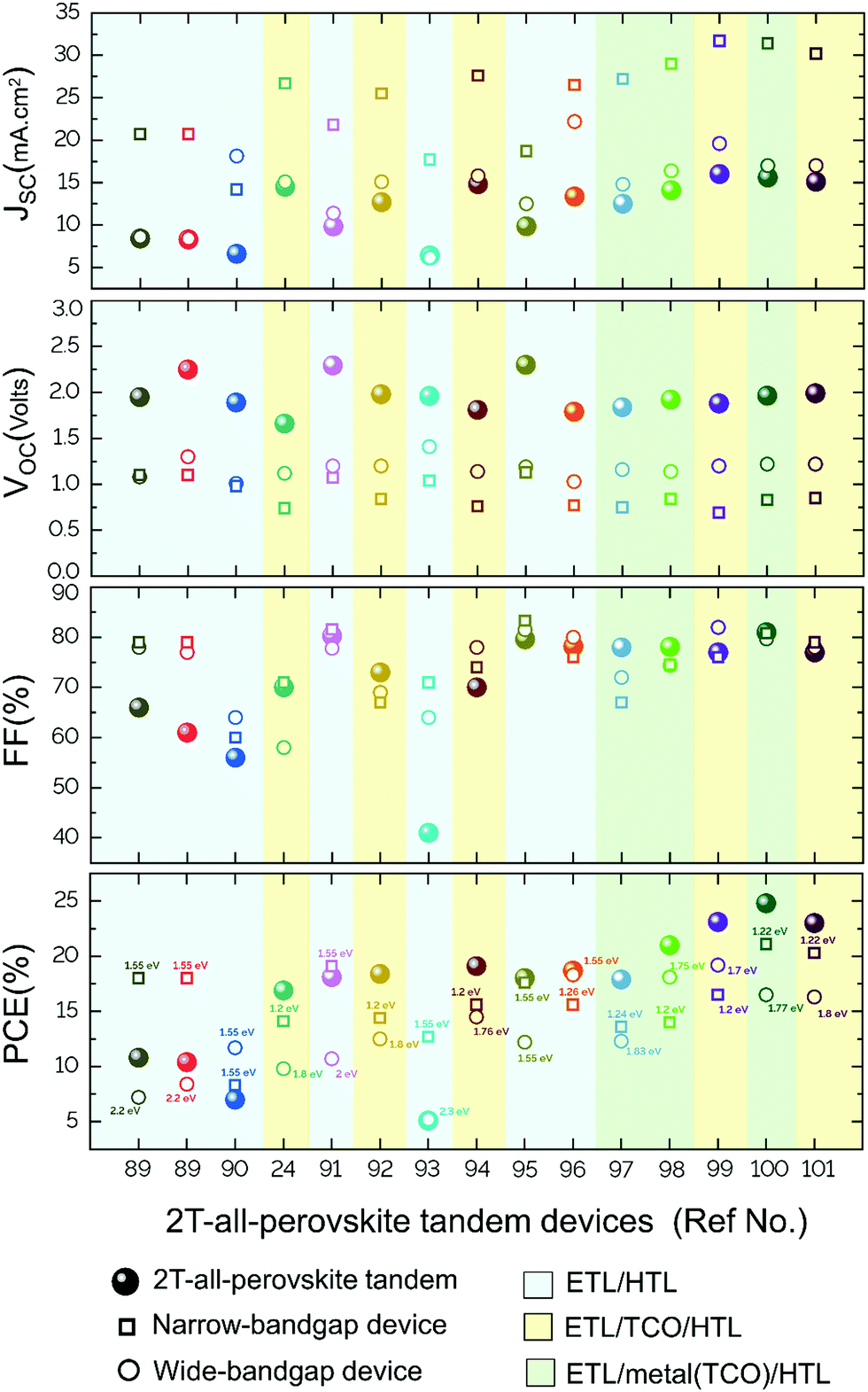 | ||
| Fig. 7 Photovoltaic device characteristics of tandem devices and individual subcells in literature for 2-terminal all-perovskite tandems, as summarized in Table 3 and are classified according to the structure of the RJ layer. (Spheres, squares, and hollow circles correspond to the champion parameters of the tandem device, the narrow-bandgap top-cell and the wide-bandgap bottom-cell employed in the reports, respectively.). | ||
As discussed, a strategy to enhance interband recombination is via TAT, e.g. by introducing a dewetted ultra-thin layer of metal (∼1 nm). Li et al. introduced an ultra-thin metallic layer of (Cu/Au) in the RJ and have achieved tandem devices with better performing FF than each of its subcells without much optical loss.92 Interestingly, the ETL stack of the bottom cell before the RJ layers in this study introduce fluoride silane – incorporated polyethylenimine ethoxylated hybrid system (FSIP) that exhibit thermionic emission – enhanced transport, providing the much-desired structural stability in the absence of robust TCOs.92 Zhao et al. employed thermally evaporated Ag metal (1 nm) and MoOx (3 nm) in combination with ITO (120 nm) as a RJ resulting in 21% PCE tandem devices.93 The introduction of ultra-thin layers of Ag/MoOx improved the VOC over ∼120 mV, and eliminated S-shape characteristics in the J–V curve near the VOC condition, demonstrating the role of the metal electrode in reducing ρc and trap mediated recombination. In a recent report by Lin et al., introducing a thin layer of Au (1 nm) in-between an ALD-SnO2/PEDOT:PSS interface acts as an effective recombination center, improving the FF of the devices from 55 to 78% with a slight improvement in VOC, without any optical (JSC) losses.95 McMeekin et al. recently demonstrated all-perovskite triple-junction monolithic tandems spanning different bandgaps.98 The device architecture used a solution-processed PEDOT:PSS/ITO nanoparticle layer as the RJ with altered solvent composition to enable the fabrication of subsequent device layers. This proof of concept 3-junction tandem yielded a VOC as high as 2.7 V. In summary, employing a TCO or TCO/metal stack as interlayers to form a RJ in an all-perovskite tandem device appears to provide significant advantages in terms of offering structural stability for top cell fabrication and device performance. However, this approach must guarantee that any intimate contact between the perovskite absorber and the metal is avoided. Otherwise, the metal can interact with the perovskite and accelerate the degradation of the device performance.
Recombination junction in CIGS/perovskite tandem solar cells
In the case of thin-film chalcogenide-based tandem solar cells, Todorov et al., demonstrated the very first 2-T CIGS/perovskite tandem solar cells with a device efficiency up to 10.4%.102 In this early implementation, an ITO layer was overlaying the CdS buffer layer (acting as the ETL of the CIGS bottom cell). The RJ was then formed by depositing PEDOT:PSS (acting as the HTL of the perovskite top cell) onto the ITO. It is of note that CIGS tandems, due to their need for a Mo back contact are normally in the substrate p–i–n configuration. Jošt et al., improved the performance of CIGSe/perovskite devices from 3.1 to 18.2%, and later from 18.2 to 21.6% by changing the recombination interface from ZnO/PTAA to ZnO/NiOx and then ZnO/NiOx/PTAA.103 ZnO/NiOx performed better as a RJ in comparison to ZnO/PTAA, improving the VOC from 0.56 to 1.5 V, thanks to the conformal coating of the NiOx film on the rough surface of the bottom cell; such surface roughness is a typical feature of CIGS solar cells and needs to be accounted for when constructing tandems. Additionally, by passivating the NiOx/perovskite interface, the tandem VOC improved to 1.59 V, resulting in highly efficient devices. As an interesting approach, Han et al. improved the CIGS/perovskite tandem performance to 22.4% by a chemical mechanical polishing process, to enable the perovskite top cell deposition. For this, they thickened the TCO of the CIGS cells, by depositing a stack of intrinsic-ZnO (i-ZnO), boron-doped ZnO (BZO), and finally ITO, which was then polished flat.104 Alternatively, Al-Ashouri et al., recently introduced self-assembling monolayers (MeO-2PACz and 2PACz) as workfunction modifiers on top of ITO, removing the need for PTAA HTL in the perovskite top cell stack.105 The SAM layer also seems to improve the performance on single-junction perovskites acting as a passivating contact, improving the lifetime of the perovskite without quenching the PL emission as in the PTAA contact. By doing so, they achieved a certified perovskite-CIGS tandem with PCE of 23.16% via a conformal modification of the ITO. Notably, as the SAM acts as the perovskite-HTL, the surface-modified ITO is now the RJ.Characterization of the recombination junction
Experimental investigations of the optical and electrical properties of the RJ are sophisticated processes and a standardized technique for this – and the definition of key diagnostic parameters – is yet to be established. Indeed, the interlayers included in the device stack, together with the photoactive/absorber and contact materials, can easily overshadow the optical and electrical properties of the RJ. Fig. 8 summarizes potential techniques that can be used to study the RJ from an electrical, optical, and structural point-of-view. For the electrical characterization (Fig. 8a), a first and immediate method to understand the electronic properties is to evaluate the diode's performance of the two layers forming the junction. Examples of this approach are common among III–V multi-junction tandem research.106–108 Similarly, ρc measurements, such as the (transversal) Cox and Strack and (coplanar) transfer length methods (TLM), have already given valuable information in the case of silicon/perovskite tandems, as proved by Shen et al. by studying RJs composed of p+-Si/TiO2.59 Another approach consists in the fabrication of three-terminal tandem devices. In this case, the third terminal is placed on the RJ itself, and the properties of the two subcells (VOC and FF for example) can then be studied separately.68 However, the three-terminal method requires the protection of the RJ layer during the processing, which may complicate the fabrication process for the different layout of the contacts. Also, this strategy is compromised for RJs with the low lateral conductivity, such as those based on nc-Si. Therefore, an easier method to study the electrical properties of the RJ and in parallel the performances of the top cell, can be realized by using a “test-structure” passivated silicon wafer, which works as a substrate and bottom contact without any role in the PV process. With this technique, the VOC, FF, and JSC of the top cell can be independently revealed for different materials and technologies used in the RJ. Moreover, this approach is particularly useful to study the RJ and the top cell performances in tandem configuration with textured surfaces, since the “dummy” wafer can be textured similarly to the bottom cell, which is hard to mimic on glass substrates. Overall, these electrical characterizations will provide useful information to optimize the RJ in terms of contact resistivity, diode performances, and voltage losses.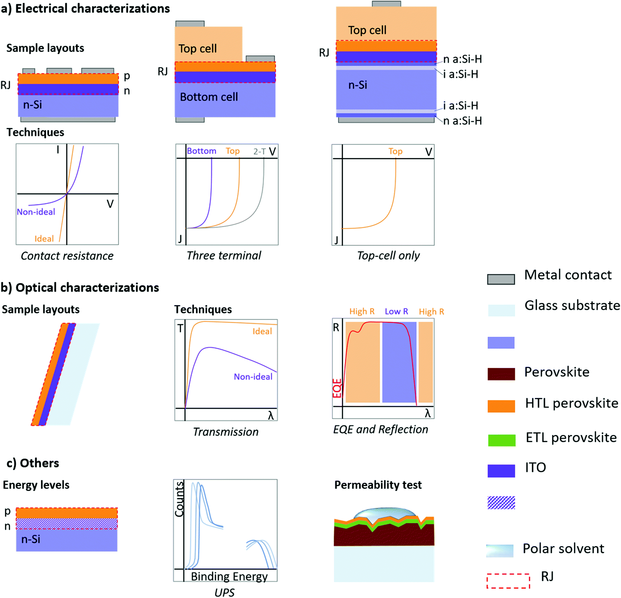 | ||
| Fig. 8 Different techniques to study the electrical, optical, and structural properties of the RJ. Presented both for silicon/perovskite or all-perovskite tandems, including a sample layout for the respective technique. (a) Electrical characterization: contact resistance, three-terminal tandem, subcell approach; for each technique we report an example of the measurement outcome. (b) Optical characterization: UV-Vis and NIR transmission, EQE and reflection. (c) Structural characterization: UPS spectroscopy for energy level evaluation, permeability experiment to test the barrier properties in all-perovskite tandems. | ||
To characterize the optical properties of the RJs, EQE and IQE techniques are almost standard techniques for daily experiments. However, since EQE and IQE measurements will give the overall response of the tandem devices, to disentangle the RJ from the stack, other optical techniques can be used: optical transmittance and reflectance spectra by spectrophotometry, and spectroscopic ellipsometry techniques for the deposited layer on glass or silicon wafers (Fig. 8b). With these methods, parasitic absorption originating from the RJs and back reflectivity of these layers can be analyzed. In this way, for example, evaluating the parasitic absorption losses that affect the current matching induced by the high concentration of free-carriers in the RJ. Ideally, the RJ should have a high near-infrared transparency in the spectrum region where the bottom cell absorbs and high reflectivity in the blue spectra where the top cell works.
Finally, there are several other characterization methods that can be used to evaluate the energetic and structural properties of the RJ (Fig. 8c). Ultraviolet photoelectron spectroscopy (UPS) is a powerful tool to determine the energy level alignment of the RJ layers. Importantly, due to the thickness of the RJ's layers, the test sample should be prepared as close to the underlying cell of the tandem. Combined with transmission data, UPS measurements give guidance to optimize WF values of the RJ layers. For all-perovskite tandems, the RJ plays the important role of protective layer for the processing of the bottom cell. Permeability tests of the RJ with polar solvents harmful for the perovskite under-layer, are useful and easy methods to fine-tune the thickness of the RJ's layers. Lastly, conventional surface and roughness characterizations, such as cross-section SEM imaging and atomic force microscopy (AFM), are powerful tools to evaluate the morphology and topography of the RJ, particularly in RJ with rough or textured interfaces, such as textured silicon bottom cells, all-perovskite tandems, and perovskite-CIGS tandems.
Outlook for new generation recombination junctions
Considering the above discussed examples, further development of RJs is critical for the evolution of perovskite-based tandems. Currently, new classes of materials, which are mostly emerging from the single-junction solar cell counterparts, are being developed. As a promising concept, Al-Ashouri et al. introduced self-assembled monolayers (SAM) with HTL properties in tandem solar cells, which is also serving as the RJ together with the ITO electrodes.109–111 Such materials systems have already been widely studied in single-junction organic and PSCs and several examples are available in the literature, especially for the electron selective contacts.109,110,112–117 On the tandem side, SAM HTLs hold great potential on rough surfaces such as CIGS-, and textured c-Si-based tandems.111 This is particularly encouraging, since the efficient electron blocking character perfectly fits in the p–i–n silicon/perovskite tandems, which has the potential to replace the conventionally used PTAA or NiOx. RJs with SAM materials may lead to new developments if their working principles and structures can be more fully understood. On the other hand, there are still many unanswered questions about such RJs, for instance their applicability on various surfaces such as TCOs and a variety of metal oxides, and particularly their long term stability. Therefore, more effort is needed for the future utilization of such materials in tandem solar cells.Conclusions
The fundamental understanding of the mechanisms that govern the recombination in perovskite tandems will push the research to test new materials and designs of the RJ, with the common goal to improve the performances of the tandems. Currently, we have seen the successful inclusion of TCOs in both silicon/perovskite, all-perovskite, and CIGS/perovskite tandems. However, for new designs, inspiration can be taken either from III–V multijunctions solar cells, or from organic PV. From the first, we have already mentioned the importance of controlling the doping level to realize efficient tunneling diodes; from the latter, we have already found useful the presence of a thin metal layer within the RJ, to favor the TAT mechanism. Moreover, all-perovskite tandems share the same requirements of organic PV for chemical robustness of the RJ, to protect the underlying layers during cell processing. In terms of new materials, the SAM technology is already arising, paving the way for new types of RJs, combining superior device performance with ease of manufacture at affordable cost. Parallel to this research, the development of large-area tandems will require the scaling up of the RJ, which will be increasingly significant as perovskite-based tandem technology approaches the PV market. Collectively, these efforts will keep improving the recombination of electron and holes from the top and bottom cell, towards more efficient tandems.Conflicts of interest
There are no conflicts to declare.Acknowledgements
The authors acknowledge the support of the King Abdullah University of Science and Technology (KAUST) Office of Sponsored Research (OSR) under award no. KAUST OSR-CARF URF/1/3097, and KAUST OSR-CRG URF/1/3383.References
- E. H. Jung, N. J. Jeon, E. Y. Park, C. S. Moon, T. J. Shin, T.-Y. Yang, J. H. Noh and J. Seo, Nature, 2019, 567, 511–515 CrossRef.
- Q. Jiang, Y. Zhao, X. Zhang, X. Yang, Y. Chen, Z. Chu, Q. Ye, X. Li, Z. Yin and J. You, Nat. Photonics, 2019, 13, 460–466 CrossRef.
- M. Kim, G.-H. Kim, T. K. Lee, I. W. Choi, H. W. Choi, Y. Jo, Y. J. Yoon, J. W. Kim, J. Lee and D. Huh, Joule, 2019, 3, 2179–2192 CrossRef.
- NREL National Center for Photovoltaics (NCPV), 2020, https://www.nrel.gov/pv/cell-efficiency.html Search PubMed.
- S. De Wolf, J. Holovsky, S.-J. Moon, P. Löper, B. Niesen, M. Ledinsky, F.-J. Haug, J.-H. Yum and C. Ballif, J. Phys. Chem. Lett., 2014, 5, 1035–1039 CrossRef.
- T. Leijtens, K. A. Bush, R. Prasanna and M. D. McGehee, Nat. Energy, 2018, 3, 828–838 CrossRef.
- Z. Ni, C. Bao, Y. Liu, Q. Jiang, W.-Q. Wu, S. Chen, X. Dai, B. Chen, B. Hartweg, Z. Yu, Z. Holman and J. Huang, Science, 2020, 367, 1352–1358 CrossRef.
- T. A. Doherty, A. J. Winchester, S. Macpherson, D. N. Johnstone, V. Pareek, E. M. Tennyson, S. Kosar, F. U. Kosasih, M. Anaya and M. Abdi-Jalebi, Nature, 2020, 580, 360–366 CrossRef.
- S. D. Stranks, G. E. Eperon, G. Grancini, C. Menelaou, M. J. Alcocer, T. Leijtens, L. M. Herz, A. Petrozza and H. J. Snaith, Science, 2013, 342, 341–344 CrossRef.
- M. Ledinsky, T. Schönfeldová, J. Holovský, E. Aydin, Z. K. Hájková, L. Landová, N. Neyková, A. Fejfar and S. De Wolf, J. Phys. Chem. Lett., 2019, 10, 1368–1373 CrossRef.
- B. Chen, S.-W. Baek, Y. Hou, E. Aydin, M. De Bastiani, B. Scheffel, A. Proppe, Z. Huang, M. Wei and Y.-K. Wang, Nat. Commun., 2020, 11, 1–9 Search PubMed.
- S. De Wolf, A. Descoeudres, Z. C. Holman and C. Ballif, Green, 2012, 2, 7–24 Search PubMed.
- C. Battaglia, A. Cuevas and S. De Wolf, Energy Environ. Sci., 2016, 9, 1552–1576 RSC.
- N. M. Haegel, H. Atwater, T. Barnes, C. Breyer, A. Burrell, Y.-M. Chiang, S. De Wolf, B. Dimmler, D. Feldman and S. Glunz, Science, 2019, 364, 836–838 CrossRef.
- M. T. Hörantner and H. J. Snaith, Energy Environ. Sci., 2017, 10, 1983–1993 RSC.
- S. E. Sofia, J. P. Mailoa, D. N. Weiss, B. J. Stanbery, T. Buonassisi and I. M. Peters, Nat. Energy, 2018, 3, 387–394 CrossRef.
- F. Rubinelli, J. Rath and R. Schropp, J. Appl. Phys., 2001, 89, 4010–4018 CrossRef.
- L. Esaki, Science, 1974, 183, 1149–1155 CrossRef.
- L. Esaki, Phys. Rev., 1958, 109, 603 CrossRef.
- M. Hermle, G. Letay, S. Philipps and A. W. Bett, Prog. Photovoltaics Res. Appl., 2008, 16, 409–418 CrossRef.
- M. Yamaguchi, Sol. Energy Mater. Sol. Cells, 2003, 75, 261–269 CrossRef.
- M. Yamaguchi, K.-I. Nishimura, T. Sasaki, H. Suzuki, K. Arafune, N. Kojima, Y. Ohsita, Y. Okada, A. Yamamoto and T. Takamoto, Sol. Energy, 2008, 82, 173–180 CrossRef.
- K. A. Bush, A. F. Palmstrom, J. Y. Zhengshan, M. Boccard, R. Cheacharoen, J. P. Mailoa, D. P. McMeekin, R. L. Hoye, C. D. Bailie and T. Leijtens, Nat. Energy, 2017, 2, 1–7 Search PubMed.
- G. E. Eperon, T. Leijtens, K. A. Bush, R. Prasanna, T. Green, J. T.-W. Wang, D. P. McMeekin, G. Volonakis, R. L. Milot and R. May, Science, 2016, 354, 861–865 CrossRef.
- T. G. Allen, J. Bullock, X. Yang, A. Javey and S. De Wolf, Nat. Energy, 2019, 1–15 Search PubMed.
- S. Zhong, J. Dreon, Q. Jeangros, E. Aydin, S. De Wolf, F. Fu, M. Boccard and C. Ballif, Adv. Funct. Mater., 2020, 30, 1907840 CrossRef.
- Z. C. Holman, M. Filipič, A. Descoeudres, S. De Wolf, F. Smole, M. Topič and C. Ballif, J. Appl. Phys., 2013, 113, 013107 CrossRef.
- Y. Wen-Jie, Z. Xiang-Bo, P. Wen-Bo, L. Shi-Yong, X. Xiao-Bing, W. Chao and L. Xian-Bo, Chin. Phys. B, 2011, 20, 078402 CrossRef.
- L. Gui-Jun, H. Guo-Fu, H. Xiao-Yan, Y. Yu-Jie, W. Chang-Chun, S. Jian, Z. Yin and G. Xin-Hua, Chin. Phys. B, 2009, 18, 1674 CrossRef.
- J. Löffler, A. Gordijn, R. Stolk, H. Li, J. Rath and R. Schropp, Sol. Energy Mater. Sol. Cells, 2005, 87, 251–259 CrossRef.
- A. Tomasi, B. Paviet-Salomon, Q. Jeangros, J. Haschke, G. Christmann, L. Barraud, A. Descoeudres, J. P. Seif, S. Nicolay and M. Despeisse, Nat. Energy, 2017, 2, 1–8 Search PubMed.
- H. Sai, T. Matsui and K. Matsubara, Appl. Phys. Lett., 2016, 109, 183506 CrossRef.
- F. Sahli, B. A. Kamino, J. Werner, M. Bräuninger, B. Paviet-Salomon, L. Barraud, R. Monnard, J. P. Seif, A. Tomasi and Q. Jeangros, Adv. Energy Mater., 2018, 8, 1701609 CrossRef.
- J. P. Mailoa, C. D. Bailie, E. C. Johlin, E. T. Hoke, A. J. Akey, W. H. Nguyen, M. D. McGehee and T. Buonassisi, Appl. Phys. Lett., 2015, 106, 121105 CrossRef.
- L. Mazzarella, Y. H. Lin, S. Kirner, A. B. Morales-Vilches, L. Korte, S. Albrecht, E. Crossland, B. Stannowski, C. Case and H. J. Snaith, Adv. Energy Mater., 2019, 9, 1803241 CrossRef.
- P. Buehlmann, J. Bailat, D. Dominé, A. Billet, F. Meillaud, A. Feltrin and C. Ballif, Appl. Phys. Lett., 2007, 91, 143505 CrossRef.
- J. Geissbühler, J. Werner, S. Martin de Nicolas, L. Barraud, A. Hessler-Wyser, M. Despeisse, S. Nicolay, A. Tomasi, B. Niesen, S. De Wolf and C. Ballif, Appl. Phys. Lett., 2015, 107, 081601 CrossRef.
- X. Zhang, Y. Wan, J. Bullock, T. Allen and A. Cuevas, Appl. Phys. Lett., 2016, 109, 052102 CrossRef.
- M. Sajjad, N. Singh, M. De Bastiani, S. De Wolf and U. Schwingenschlögl, Phys. Status Solidi RRL, 2019, 13, 1900328 CrossRef CAS.
- C. Battaglia, X. Yin, M. Zheng, I. D. Sharp, T. Chen, S. McDonnell, A. Azcatl, C. Carraro, B. Ma and R. Maboudian, Nano Lett., 2014, 14, 967–971 CrossRef CAS.
- F. Menchini, M. L. Grilli, T. Dikonimos, A. Mittiga, L. Serenelli, E. Salza, R. Chierchia and M. Tucci, Phys. Status Solidi C, 2016, 13, 1006–1010 CrossRef CAS.
- T. Becker, S. Trost, A. Behrendt, I. Shutsko, A. Polywka, P. Görrn, P. Reckers, C. Das, T. Mayer and D. Di Carlo Rasi, Adv. Energy Mater., 2018, 8, 1702533 CrossRef.
- M. Houssa, M. Tuominen, M. Naili, V. Afanas’ ev, A. Stesmans, S. Haukka and M. Heyns, J. Appl. Phys., 2000, 87, 8615–8620 CrossRef CAS.
- M. Baudrit and C. Algora, IEEE Trans. Electron Devices, 2010, 57, 2564–2571 CAS.
- M. Courel, F. Pulgarín-Agudelo, J. Andrade-Arvizu and O. Vigil-Galán, Sol. Energy Mater. Sol. Cells, 2016, 149, 204–212 CrossRef CAS.
- B. Maennig, J. Drechsel, D. Gebeyehu, P. Simon, F. Kozlowski, A. Werner, F. Li, S. Grundmann, S. Sonntag and M. Koch, Appl. Phys. A: Mater. Sci. Process., 2004, 79, 1–14 CrossRef CAS.
- M. Morales-Masis, S. De Wolf, R. Woods-Robinson, J. W. Ager and C. Ballif, Adv. Electron. Mater., 2017, 3, 1600529 CrossRef.
- Z. Song, J. Werner, S. C. Watthage, F. Sahli, N. Shrestha, S. De Wolf, B. Niesen, A. B. Phillips, C. Ballif and R. J. Ellingson, IEEE J. Photovolt., 2017, 7, 1563–1568 Search PubMed.
- F. Sahli, J. Werner, B. A. Kamino, M. Bräuninger, R. Monnard, B. Paviet-Salomon, L. Barraud, L. Ding, J. J. D. Leon and D. Sacchetto, Nat. Mater., 2018, 17, 820–826 CrossRef CAS.
- X. Zheng, Y. Hou, C. Bao, J. Yin, F. Yuan, Z. Huang, K. Song, J. Liu, J. Troughton and N. Gasparini, Nat. Energy, 2020, 5, 131–140 CrossRef CAS.
- J. A. Raiford, R. A. Belisle, K. A. Bush, R. Prasanna, A. F. Palmstrom, M. D. McGehee and S. F. Bent, Sustainable Energy Fuels, 2019, 3, 1517–1525 RSC.
- E. Aydin, M. De Bastiani and S. De Wolf, Adv. Mater., 2019, 31, 1900428 CrossRef.
- M. Sajjad, X. Yang, P. Altermatt, N. Singh, U. Schwingenschlögl and S. De Wolf, Appl. Phys. Lett., 2019, 114, 071601 CrossRef.
- Z. Hu, Z. Zhong, K. Zhang, Z. Hu, C. Song, F. Huang, J. Peng, J. Wang and Y. Cao, NPG Asia Mater., 2017, 9, e379–e379 CrossRef CAS.
- J. Xu, C. C. Boyd, J. Y. Zhengshan, A. F. Palmstrom, D. J. Witter, B. W. Larson, R. M. France, J. Werner, S. P. Harvey and E. J. Wolf, Science, 2020, 367, 1097–1104 CrossRef CAS.
- B. Chen, Z. Yu, K. Liu, X. Zheng, Y. Liu, J. Shi, D. Spronk, P. N. Rudd, Z. Holman and J. Huang, Joule, 2019, 3, 177–190 CrossRef CAS.
- Y. Hou, E. Aydin, M. De Bastiani, C. Xiao, F. H. Isikgor, D.-J. Xue, B. Chen, H. Chen, B. Bahrami and A. H. Chowdhury, Science, 2020, 367, 1135–1140 CrossRef CAS.
- B. Chen, Z. J. Yu, S. Manzoor, S. Wang, W. Weigand, Z. Yu, G. Yang, Z. Ni, X. Dai, Z. C. Holman and J. Huang, Joule, 2020, 4(4), 850–864 CrossRef CAS.
- H. Shen, S. T. Omelchenko, D. A. Jacobs, S. Yalamanchili, Y. Wan, D. Yan, P. Phang, Y. Wu, Y. Yin and C. Samundsett, Sci. Adv., 2018, 4, eaau9711 CrossRef CAS.
- J. Zheng, H. Mehrvarz, F.-J. Ma, C. F. J. Lau, M. A. Green, S. Huang and A. W. Ho-Baillie, ACS Energy Lett., 2018, 3, 2299–2300 CrossRef CAS.
- J. Werner, C.-H. Weng, A. Walter, L. Fesquet, J. P. Seif, S. De Wolf, B. Niesen and C. Ballif, J. Phys. Chem. Lett., 2016, 7, 161–166 CrossRef CAS.
- J. Werner, A. Walter, E. Rucavado, S.-J. Moon, D. Sacchetto, M. Rienaecker, R. Peibst, R. Brendel, X. Niquille, S. De Wolf, P. Löper, M. Morales-Masis, S. Nicolay, B. Niesen and C. Ballif, Appl. Phys. Lett., 2016, 109, 233902 CrossRef.
- E. Aydin, J. Troughton, M. De Bastiani, E. Ugur, M. Sajjad, A. Alzahrani, M. Neophytou, U. Schwingenschlögl, F. Laquai, D. Baran and S. De Wolf, ACS Appl. Energy Mater., 2018, 1(11), 6227–6233 CrossRef.
- Y. Hou, E. Aydin, M. De Bastiani, C. Xiao, F. H. Isikgor, D.-J. Xue, B. Chen, H. Chen, B. Bahrami, A. H. Chowdhury, A. Johnston, S.-W. Baek, Z. Huang, M. Wei, Y. Dong, J. Troughton, R. Jalmood, A. J. Mirabelli, T. G. Allen, E. Van Kerschaver, M. I. Saidaminov, D. Baran, Q. Qiao, K. Zhu, S. De Wolf and E. H. Sargent, Science, 2020, 367, 1135–1140 CrossRef CAS.
- D. Grant, K. Catchpole, K. Weber and T. White, Opt. Express, 2016, 24, A1454–A1470 CrossRef CAS.
- T. Koida, H. Fujiwara and M. Kondo, Appl. Phys. Express, 2008, 1, 041501 CrossRef.
- E. Aydin, M. De Bastiani, X. Yang, M. Sajjad, F. Aljamaan, Y. Smirnov, M. N. Hedhili, W. Liu, T. G. Allen and L. Xu, Adv. Funct. Mater., 2019, 29, 1901741 CrossRef.
- I. J. Park, J. H. Park, S. G. Ji, M.-A. Park, J. H. Jang and J. Y. Kim, Joule, 2019, 3, 807–818 CrossRef CAS.
- L. D'Amario, J. Föhlinger, G. Boschloo and L. Hammarström, Chem. Sci., 2018, 9, 223–230 RSC.
- K. A. Bush, S. Manzoor, K. Frohna, Z. J. Yu, J. A. Raiford, A. F. Palmstrom, H.-P. Wang, R. Prasanna, S. F. Bent and Z. C. Holman, ACS Energy Lett., 2018, 3, 2173–2180 CrossRef CAS.
- D. Kim, H. J. Jung, I. J. Park, B. W. Larson, S. P. Dunfield, C. Xiao, J. Kim, J. Tong, P. Boonmongkolras and S. G. Ji, Science, 2020, 368, 155–160 CrossRef CAS.
- S. Albrecht, M. Saliba, J. P. C. Baena, F. Lang, L. Kegelmann, M. Mews, L. Steier, A. Abate, J. Rappich and L. Korte, Energy Environ. Sci., 2016, 9, 81–88 RSC.
- Z. Qiu, Z. Xu, N. Li, N. Zhou, Y. Chen, X. Wan, J. Liu, N. Li, X. Hao and P. Bi, Nano Energy, 2018, 53, 798–807 CrossRef CAS.
- D. A. Jacobs, M. Langenhorst, F. Sahli, B. S. Richards, T. P. White, C. Ballif, K. R. Catchpole and U. W. Paetzold, J. Phys. Chem. Lett., 2019, 10, 3159–3170 CrossRef CAS.
- M. Jošt, E. Köhnen, A. B. Morales-Vilches, B. Lipovšek, K. Jäger, B. Macco, A. Al-Ashouri, J. Krč, L. Korte and B. Rech, Energy Environ. Sci., 2018, 11, 3511–3523 RSC.
- F. Hou, C. Han, O. Isabella, L. Yan, B. Shi, J. Chen, S. An, Z. Zhou, W. Huang, H. Ren, Q. Huang, G. Hou, X. Chen, Y. Li, Y. Ding, G. Wang, C. Wei, D. Zhang, M. Zeman, Y. Zhao and X. Zhang, Nano Energy, 2019, 56, 234–240 CrossRef CAS.
- G. Nogay, F. Sahli, J. Werner, R. Monnard, M. Boccard, M. Despeisse, F. Haug, Q. Jeangros, A. Ingenito and C. Ballif, ACS Energy Lett., 2019, 4, 844–845 CrossRef CAS.
- J. Zheng, C. F. J. Lau, H. Mehrvarz, F.-J. Ma, Y. Jiang, X. Deng, A. Soeriyadi, J. Kim, M. Zhang and L. Hu, Energy Environ. Sci., 2018, 11, 2432–2443 RSC.
- C. U. Kim, J. C. Yu, E. D. Jung, I. Y. Choi, W. Park, H. Lee, I. Kim, D.-K. Lee, K. K. Hong, M. H. Song and K. J. Choi, Nano Energy, 2019, 60, 213–221 CrossRef CAS.
- Y. Wu, D. Yan, J. Peng, Y. Wan, S. P. Phang, H. Shen, N. Wu, C. Barugkin, X. Fu and S. Surve, Energy Environ. Sci., 2017, 10, 2472–2479 RSC.
- K. Yoshikawa, H. Kawasaki, W. Yoshida, T. Irie, K. Konishi, K. Nakano, T. Uto, D. Adachi, M. Kanematsu and H. Uzu, Nat. Energy, 2017, 2, 17032 CrossRef CAS.
- Z. Guo, A. K. Jena, I. Takei, G. M. Kim, M. A. Kamarudin, Y. Sanehira, A. Ishii, Y. Numata, S. Hayase and T. Miyasaka, J. Am. Chem. Soc., 2020, 142(21), 9725–9734 CAS.
- J. R. M. Werner, L. Barraud, A. Walter, M. Bräuninger, F. Sahli, D. Sacchetto, N. Tétreault, B. Paviet-Salomon, S.-J. Moon and C. Allebé, ACS Energy Lett., 2016, 1, 474–480 CrossRef CAS.
- J. H. Heo and S. H. Im, Adv. Mater., 2016, 28, 5121–5125 CrossRef CAS.
- F. Jiang, T. Liu, B. Luo, J. Tong, F. Qin, S. Xiong, Z. Li and Y. Zhou, J. Mater. Chem. A, 2016, 4, 1208–1213 RSC.
- D. Forgács, L. Gil-Escrig, D. Pérez-Del-Rey, C. Momblona, J. Werner, B. Niesen, C. Ballif, M. Sessolo and H. J. Bolink, Adv. Energy Mater., 2017, 7, 1602121 CrossRef.
- A. Rajagopal, Z. Yang, S. B. Jo, I. L. Braly, P. W. Liang, H. W. Hillhouse and A. K. Y. Jen, Adv. Mater., 2017, 29, 1702140 CrossRef.
- R. Sheng, M. T. Hörantner, Z. Wang, Y. Jiang, W. Zhang, A. Agosti, S. Huang, X. Hao, A. Ho-Baillie and M. Green, J. Phys. Chem. C, 2017, 121, 27256–27262 CrossRef CAS.
- T. Leijtens, R. Prasanna, K. A. Bush, G. E. Eperon, J. A. Raiford, A. Gold-Parker, E. J. Wolf, S. A. Swifter, C. C. Boyd and H.-P. Wang, Sustainable Energy Fuels, 2018, 2, 2450–2459 RSC.
- J. Ávila, C. Momblona, P. Boix, M. Sessolo, M. Anaya, G. Lozano, K. Vandewal, H. Míguez and H. J. Bolink, Energy Environ. Sci., 2018, 11, 3292–3297 RSC.
- C.-Y. Chang, B.-C. Tsai, Y.-C. Hsiao, M.-Z. Lin and H.-F. Meng, Nano Energy, 2019, 55, 354–367 CrossRef CAS.
- C. Li, Z. S. Wang, H. L. Zhu, D. Zhang, J. Cheng, H. Lin, D. Ouyang and W. C. Choy, Adv. Energy Mater., 2018, 8, 1801954 CrossRef.
- D. Zhao, C. Chen, C. Wang, M. M. Junda, Z. Song, C. R. Grice, Y. Yu, C. Li, B. Subedi and N. J. Podraza, Nat. Energy, 2018, 3, 1093–1100 CrossRef CAS.
- A. F. Palmstrom, G. E. Eperon, T. Leijtens, R. Prasanna, S. N. Habisreutinger, W. Nemeth, E. A. Gaulding, S. P. Dunfield, M. Reese and S. Nanayakkara, Joule, 2019, 3, 2193–2204 CrossRef CAS.
- R. Lin, K. Xiao, Z. Qin, Q. Han, C. Zhang, M. Wei, M. I. Saidaminov, Y. Gao, J. Xu and M. Xiao, Nat. Energy, 2019, 4, 864–873 CrossRef CAS.
- Z. Yang, Z. Yu, H. Wei, X. Xiao, Z. Ni, B. Chen, Y. Deng, S. N. Habisreutinger, X. Chen and K. Wang, Nat. Commun., 2019, 10, 1–9 CrossRef.
- N. J. Jeon, J. H. Noh, W. S. Yang, Y. C. Kim, S. Ryu, J. Seo and S. I. Seok, Nature, 2015, 517, 476–480 CrossRef CAS.
- D. P. McMeekin, S. Mahesh, N. K. Noel, M. T. Klug, J. Lim, J. H. Warby, J. M. Ball, L. M. Herz, M. B. Johnston and H. J. Snaith, Joule, 2019, 3, 387–401 CrossRef CAS.
- T. Jesper Jacobsson, J.-P. Correa-Baena, M. Pazoki, M. Saliba, K. Schenk, M. Gratzel and A. Hagfeldt, Energy Environ. Sci., 2016, 9, 1706–1724 RSC.
- M. T. Hörantner, T. Leijtens, M. E. Ziffer, G. E. Eperon, M. G. Christoforo, M. D. McGehee and H. J. Snaith, ACS Energy Lett., 2017, 2, 2506–2513 CrossRef.
- F. Jiang, T. Liu, B. Luo, J. Tong, F. Qin, S. Xiong, Z. Li and Y. Zhou, J. Mater. Chem. A, 2016, 4, 1208–1213 RSC.
- T. Todorov, T. Gershon, O. Gunawan, Y. S. Lee, C. Sturdevant, L.-Y. Chang and S. Guha, Adv. Energy Mater., 2015, 5, 1500799 CrossRef.
- M. Jošt, T. Bertram, D. Koushik, J. A. Marquez, M. A. Verheijen, M. D. Heinemann, E. Köhnen, A. Al-Ashouri, S. Braunger, F. Lang, B. Rech, T. Unold, M. Creatore, I. Lauermann, C. A. Kaufmann, R. Schlatmann and S. Albrecht, ACS Energy Lett., 2019, 4, 583–590 CrossRef.
- Q. Han, Y.-T. Hsieh, L. Meng, J.-L. Wu, P. Sun, E.-P. Yao, S.-Y. Chang, S.-H. Bae, T. Kato, V. Bermudez and Y. Yang, Science, 2018, 361, 904–908 CrossRef CAS.
- A. Al-Ashouri, A. Magomedov, M. Roß, M. Jošt, M. Talaikis, G. Chistiakova, T. Bertram, J. A. Márquez, E. Köhnen, E. Kasparavičius, S. Levcenco, L. Gil-Escrig, C. J. Hages, R. Schlatmann, B. Rech, T. Malinauskas, T. Unold, C. A. Kaufmann, L. Korte, G. Niaura, V. Getautis and S. Albrecht, Energy Environ. Sci., 2019, 12, 3356–3369 RSC.
- W. Guter and A. W. Bett, IEEE Trans. Electron Devices, 2006, 53, 2216–2222 CAS.
- W. Guter and A. W. Bett, 2006.
- V. Andreev, E. Ionova, V. Larionov, V. Rumyantsev, M. Shvarts and G. Glenn, 2006.
- A. Magomedov, A. Al-Ashouri, E. Kasparavičius, S. Strazdaite, G. Niaura, M. Jošt, T. Malinauskas, S. Albrecht and V. Getautis, Adv. Energy Mater., 2018, 8, 1801892 CrossRef.
- A. Al-Ashouri, A. Magomedov, M. Roß, M. Jošt, M. Talaikis, G. Chistiakova, T. Bertram, J. A. Márquez, E. Köhnen and E. Kasparavičius, Energy Environ. Sci., 2019, 12, 3356–3369 RSC.
- M. Jošt, T. Bertram, D. Koushik, J. A. Marquez, M. A. Verheijen, M. D. Heinemann, E. Köhnen, A. Al-Ashouri, S. Braunger and F. Lang, ACS Energy Lett., 2019, 4, 583–590 CrossRef.
- K. Wojciechowski, T. Leijtens, S. Siprova, C. Schlueter, M. T. Hörantner, J. T.-W. Wang, C.-Z. Li, A. K.-Y. Jen, T.-L. Lee and H. J. Snaith, J. Phys. Chem. Lett., 2015, 6, 2399–2405 CrossRef CAS.
- P. Topolovsek, F. Lamberti, T. Gatti, A. Cito, J. Ball, E. Menna, C. Gadermaier and A. Petrozza, J. Mater. Chem. A, 2017, 5, 11882–11893 RSC.
- Y. Zhang, P. Wang, X. Yu, J. Xie, X. Sun, H. Wang, J. Huang, L. Xu, C. Cui and M. Lei, J. Mater. Chem. A, 2016, 4, 18509–18515 RSC.
- C. Xiao, C. Wang, W. Ke, B. P. Gorman, J. Ye, C.-S. Jiang, Y. Yan and M. M. Al-Jassim, ACS Appl. Mater. Interfaces, 2017, 9, 38373–38380 CrossRef CAS.
- A. Tada, Y. Geng, M. Nakamura, Q. Wei, K. Hashimoto and K. Tajima, Phys. Chem. Chem. Phys., 2012, 14, 3713–3724 RSC.
- S. Khodabakhsh, D. Poplavskyy, S. Heutz, J. Nelson, D. D. Bradley, H. Murata and T. S. Jones, Adv. Funct. Mater., 2004, 14, 1205–1210 CrossRef CAS.
| This journal is © The Royal Society of Chemistry 2020 |