
 Open Access Article
 This Open Access Article is licensed under a
 Creative Commons Attribution 3.0 Unported Licence
Defects in complex oxide thin films for electronics and energy applications: challenges and opportunities
Weiwei
Li
 *a,
Jueli
Shi
b,
Kelvin H. L.
Zhang
*b and
Judith L.
MacManus-Driscoll
*a
*a,
Jueli
Shi
b,
Kelvin H. L.
Zhang
*b and
Judith L.
MacManus-Driscoll
*a
aDepartment of Materials Science and Metallurgy, University of Cambridge, 27 Charles Babbage Road, Cambridge, CB3 0FS, UK. E-mail: wl337@cam.ac.uk; jld35@cam.ac.uk
bState Key Laboratory of Physical Chemistry of Solid Surfaces, College of Chemistry and Chemical Engineering, Xiamen University, Xiamen 361005, China. E-mail: kelvinzhang@xmu.edu.cn
First published on 21st July 2020
Abstract
Complex transition-metal oxides (TMOs) are critical materials for cutting-edge electronics and energy-related technologies, on the basis of their intriguing properties including ferroelectricity, magnetism, superconductivity, (photo- and electro-) catalytic activity, ionic conductivity, etc. These properties are fundamentally determined by the partially occupied TM d orbitals and the corresponding local coordination environments, which are sensitive to defects (or impurities), compositions, grain boundaries, surface and interfaces, etc. Recently, motivated by the advance in thin film epitaxy techniques, the complex oxide research community has shown great interest in controlling defects for enhanced or even unprecedented functional properties. In this review, we provide an overview on recent progress in tuning the functional properties of TMO thin films via defect engineering. We begin with a brief introduction to the defect chemistry of TMOs, including types of defects and their effects on local atomic structure, electron configurations and electronic structure, etc. We then review recent research efforts in engineering defects in TMOs for novel functionalities, such as ferroelectricity, magnetism, multi-ferroelectricity and dielectricity, two-dimensional electron/hole gas, metal–insulator transitions, resistive switching, ionic conductivity, photo-electrocatalysis, etc. We also provide insights into understanding the defect-structure–property relationship from the perspective of electronic structure. Finally, challenges and perspectives on control of defects for design of novel devices are discussed.
 Weiwei Li | Weiwei Li received his PhD degree from Soochow University in 2015. Currently, he is a research associate in the Department of Materials Science & Metallurgy at the University of Cambridge. His research interests focus on the complex functional oxide thin films for (opto-)electronic devices and energy conversion/storage. |
 Jueli Shi | Jueli Shi received his bachelor degree in energy chemistry from Xiamen University in 2018. He is currently a PhD candidate at college of Chemistry and Chemical Engineering, Xiamen University under the supervision of Prof. Kelvin H. L. Zhang. His research interest focusses on the synthesis and properties of oxide semiconductor thin films. |
 Kelvin H. L. Zhang | Prof. Kelvin H. L. Zhang is a professor at college of Chemistry and Chemical Engineering, Xiamen University. His current research interests focus on the synthesis and properties of complex metal oxide thin films and heterostructures relevant to application in oxide electronics and electrocatalysts. He obtained his PhD degree in chemistry Oxford University of in 2012, followed by working as a postdoc at Pacific Northwest National Laboratory and as a Herchel Smith Fellow at University of Cambridge from 2015 to 2017. |
 Judith L. MacManus-Driscoll | Prof. Judith MacManus-Driscoll is Professor in the Materials Science & Metallurgy at the University of Cambridge. She is also Royal Academy of Engineering Chair in Emerging Technologies. Her research work is in the area of oxide thin film engineering for low power electronic and energy devices. She is interested both in understanding basic functionalities and in engineering new interfacial-driven properties. |
1. Background for complex transition-metal oxides
Complex transition-metal oxides (TMOs) have attracted intensive research interests in both materials science and condensed matter physics over the past decades, largely due to their broad range of properties from insulating to semiconducting or metallic, exhibiting many fascinating phenomena including (anti-)ferromagnetism (FM), (anti-)ferroelectricity (FE), multi-ferroelectricity, ionic conduction, colossal magnetoresistance (CMR) and high temperature superconductivity, etc. These exotic properties arise from a complex hierarchy of competing interactions among spin, charge, orbital and lattice degrees of freedom, which are fundamentally underpinned by the electronic states of the partially occupied TM d orbitals. Driven by recent advances in fabrication of high-quality epitaxial thin films with an atomic-scale control via pulsed laser deposition (PLD) and molecular-beam epitaxy (MBE), TMOs are receiving fast-growing interests and hold great potential to outperform conventional semiconductors. However, the epitaxial thin films required for most applications are imperfect with far from optimum performance. Hence, many promised applications spanning beyond-Si information and communications technology (ICT) devices to a vast range of energy-related devices and sensors currently remain just promises. Furthermore, TMOs are also promising candidates as (photo-)electrocatalysts for the production of “green fuels” (principally H2, syngas and even liquid hydrocarbons) by splitting H2O and reducing CO2 and as electrocatalysts and ionic conductors in solid oxide fuel cells (SOFCs) for the combustion of “green fuels” (e.g., H2) to generate electricity with high efficiency. The production and use of “green fuels” are widely seen as a promising pathway towards a global sustainable energy future.In the field of microelectronics, the properties of IV elemental semiconductors (e.g., Si), III–V compound semiconductors (e.g., GaAs), II–VI compound semiconductors (e.g., ZnO) and their implementation in devices such as transistors, photodetectors, light-emitting diodes, and solar cells depend on the control and distribution of defects, dopants, surface and interface electronic states, with spatial scale often on the sub-part-per-million level. Recently, with the simultaneous advances in thin film synthesis, characterization, and modelling of TMOs, engineering the defects and interface in TMOs have been widely explored as a route to enhance and even create novel functionalities in TMOs for new devices.1 Although significant progresses have been made in the past decade (will be discussed later), a deep understanding of the defect chemistry in complex TMOs still lag behind that in conventional semiconductors. This is because: (1) TMOs have many constituent elements and can accommodate a wide variety of defects, including oxygen vacancies (VO), cation vacancies (VC), interstitial defects, local structural distortions, grain boundaries, domain walls, misfit dislocations, and impurities such as H+/−, Li+, etc. (2) Due to the ionic nature of TMOs, the transition energy of defects in TMOs are usually high and the extra charges left by defects are usually localized, therefore defects in TMOs usually cannot lead to a significant change in the electrical conductivity as present in conventional semiconductors. (3) Although theoretical modeling has also been widely used to study the thermodynamics and electronic states of defects, the fundamental issue of ab initio density functional theory (DFT) in dealing with the many-electron system gives rise to a considerable underestimation of the bandgap of TMOs, and therefore leads to many inaccuracies in predicting the properties of defects.2–4
In this review, we will provide an overview on recent progress in tuning the functional properties of complex TMO thin films via defect engineering. We will begin with a brief introduction on the types of defects and their consequences on electronic structures. We will then provide a detailed review on how these defects can change functional properties (e.g., ferroelectricity, magnetism, multi-ferroelectricity, dielectricity, optical and transport properties, ionic conduction, and photo-electrocatalytic activity) and how these properties can be experimentally analyzed and evaluated. Finally, challenges and perspectives of tailoring TMOs properties through defect engineering are discussed.
2. Defect chemistry in complex transition-metal oxides
2.1 Types of defects
Since this review focuses mainly on TMOs with a perovskite structure, we will use perovskite oxides as examples to illustrate the types of defects present in TMOs. Perovskite TMOs have a chemical formula of ABO3, as sketched in Fig. 1. A-sites are usually alkaline rare-earth cations, while B-site cations are usually TM cations with partially filled d orbitals octahedrally coordinated by six oxygen anions.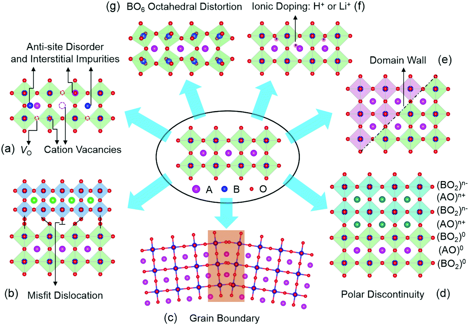 | ||
| Fig. 1 The different types of defects in transition metal oxides (TMOs). (a) VO: missing oxygen atoms from lattice sites; VC: missing cation atoms from lattice sites; anti-site disorder: swapping the cation/oxygen positions; interstitial impurities: ions occupying interstitial crystallographic sites. (b) Misfit dislocation: a missing or dangling bond in the lattice between two TMO layers with different lattice parameters. (c) Grain boundary: the interface between two grains with different crystalline orientations. (d) Polar discontinuity: the interface between nonpolar and polar TMOs. (e) Domain wall: the boundary between two neighbouring domains. (f) Ionic doping: the process of moving ions into or out of TMOs by an external stimuli. (g) BO6 octahedral distortion: the tilting of an oxygen octahedron in TMOs. | ||
Point defects represent a deviation from the long-range periodicity of crystal lattice. The key types of point defects include vacancies (e.g., oxygen vacancies, VO and cation vacancies, VC), interstitials and anti-site defects (Fig. 1a). A remarkable example can be found in the perovskite SrTiO3, where the introduction of VO can turn the insulating SrTiO3 into a metallic state, and even a dome-shaped superconducting phase dependent on carrier density concentrations.5–7 Further, the formation of Ti3+ (3d1) induced by VO can lead to a ferromagnetic interaction in diamagnetic SrTiO3.8 Through the formation of Sr vacancies, room-temperature ferroelectricity can be created in paraelectric SrTiO3.9 Moreover, by swapping the cation positions between Sr2+ and Ti4+ to form anti-site cationic defects of SrTi or TiSr, paraelectric SrTiO3 become ferroelectric at room temperature and highly conductive channels can also be formed and controlled by the ferroelectric polarization.10
Owing to the discontinuity of lattice and chemical environment, the interface provides a more favorable environment for defects with lower formation energy. These interface-related defects contain misfit dislocations (Fig. 1b), grain boundaries (Fig. 1c), polar discontinuity (Fig. 1d), and domain walls (Fig. 1e). Crystalline TMOs usually contain dislocations, grain boundaries, and domain walls, which reportedly exhibit a very different nature from the rest of the bulk matrix. The presence of these defects can significantly influence properties such as ionic and electrical conductivities, magnetism, and ferroelectricity. For instance, dislocations have been reported to creating ferromagnetic regions in anti-ferromagnetic NiO,11 while grain boundaries of ferromagnetic La2/3Ca1/3MnO3 can lead to paramagnetic properties.12 In SrTiO3, the dislocations and grain boundaries are generally considered to be charged largely due to nonstoichiometry, which may account for the unique electrical and ionic transport properties.13,14 Also, electronic conductivity has been observed at ferroelectric domain walls in the insulating multiferroic BiFeO3.15
Oxygen octahedra (BO6, Fig. 1g) plays a central role in the physical properties of many ABO3 compounds. Their rotations lead to the reduction of the B–O–B bond angle, with profound consequences for magnetic and transport properties of various perovskite TMOs. In the rare-earth (R) nickelate RNiO3 series of compounds, the reduction of the Ni–O–Ni bond angle is accompanied by a spectacular first-order metal-to-insulator transition,16 whereas the magnetic superexchange interaction in manganites depends sensitively on the Mn–O–Mn bond angle and bond length.17 Besides, reversible changes in the structural and electronic properties of TMOs can be achieved with electric fields by moving ions (e.g., H+ and Li+, Fig. 1f) into or out of TMOs.18–21
2.2 Electronic structure consequences of defects
Due to the strong interactions between structural and electronic structures, coherently strained TMOs films and heterostructures have emerged as one of the most effective platforms to engineer novel functionalities. The nature of BO6 rotations and structural deviations from ideal cubic symmetry to alter key structural features like B–O bond lengths strongly influences TMOs electronic structure through properties such as d orbital occupancy and metal–oxygen orbital overlap. Tuning B–O bond lengths of TMOs by strain can break the degeneracy of eg orbitals by enhancing the electron occupancy in either in-plane dx2−y2 orbital under tensile strain or the out-of-plane dz2 orbital under compressive strain (Fig. 2a).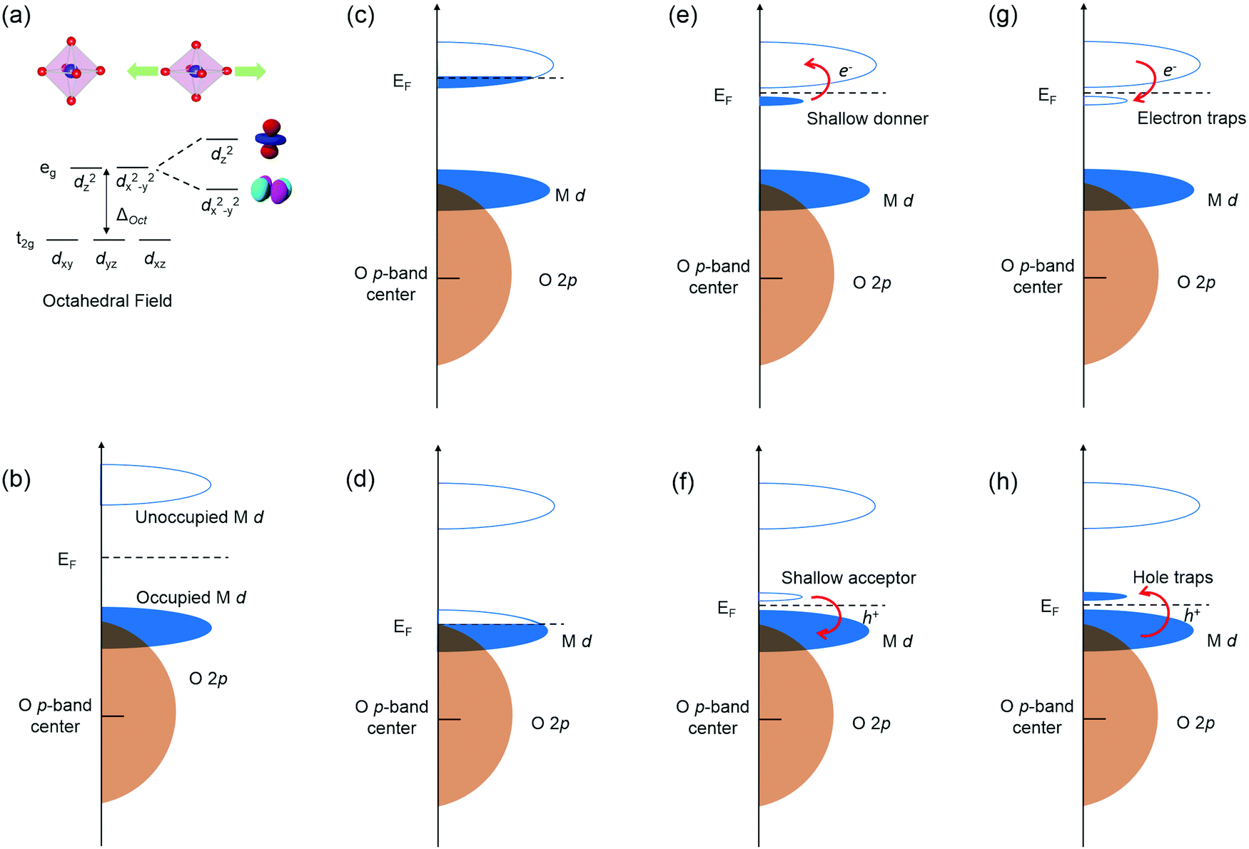 | ||
| Fig. 2 Electronic Structure of transition metal oxide and the typical defect states within it: (a) d orbital splitting of transition metal oxides through octahedral field. (b) Idealistic band structure. (c) and (d) Extra electrons or holes in conduction band (CB) or valence band (VB). (e) and (f) Defect levels providing free electrons or holes by thermal excitation. (g) and (h) Defect levels acting as traps for electrons and holes. | ||
Defects, impurities and interface break the regular periodicity of the crystal lattice, and more importantly introduce extra energy levels into the band gap, therefore leading to the change of electronic structure and physical properties of TMOs. The band structure of TMOs generally contains an empty TM nd derived conduction band (CB) and valence band (VB) with O 2p6 hybridized with filled TM nd orbitals (Fig. 2b). The energy separation of the empty TM nd and filled TM nd orbitals is induced by the crystal field splitting and/or the intra-atomic electron–electron repulsion energies (Un). The formation of defects in TMOs will introduce extra electronic states in the bands, leading to a range of novel physical properties.22–25 The most critical factors of the defects include: (i) the energy positions of extra defect states relative to CB/VB; (ii) the local environment of the defects (coordination numbers and bonding length/angle); (iii) the number of occupied carriers, as schematic illustrated in Fig. 2c–h.
When extra electrons are introduced into the CB or extra holes into the VB, TMOs will become more conductive and sometimes a metallic state can be induced, as shown in Fig. 2c and d. More commonly seen cases would be defect levels with electrons located just below the CB, or the empty level located just above the VB, acting as shallow donors and shallow acceptors (Fig. 2e and f). Under these circumstances, defect levels could provide free electrons or holes by thermal excitation and increase the conductivity. Moreover, the Fermi level will also be changed. When the empty defect levels are located just below the bottom of CB, or levels with electrons are just above the top of VB, the defects will no longer introduce new carriers into the bands or alter the Fermi level, and in turn act as traps for electrons in CB or holes in VB, as shown in Fig. 2g–h. Sometimes the defect levels are far from the band edges, so that the free carriers cannot be generated under normal thermal excitations, these defects are known as deep states.
The creation of defects in ionic oxides such as MgO is difficult, due to the high formation energies.26,27 However, many TMOs can tolerate high concentrations of defects under equilibrium conditions. These defects are often associated with deviation from ideal stoichiometry of the parent oxides, due to the relative ease of reducing or oxidizing of the metal ions.23,28,29 Shallow levels are often induced with the break of perfect stoichiometry and determine the conducting behaviors of the resulted TMOs. The nonstoichiometry of TMOs could be divided into metal excess and oxygen excess. The metal excess of oxide MaOb could be achieved by the introduction of VO with a formula of MaOb−δ, or through the introduction of metal cation interstitials with a formula of Ma+δOb. In both cases, the nonstoichiometry results in the involvement of additional electrons and the related electronic properties depend on the extent of the electrons’ binding strength to cationic species. Once sufficient energies are provided to the metal excess oxides, electrons become itinerant and the oxides become n-type conductive. For example, SrTiO3 could form Ti interstitials or VO to become a n-type semiconductor, or even a metallic state as mentioned in above section.30–32 Similarly, p-type conductivity could be achieved by extra holes introduced in oxygen-excess phases. These phases can be created by the introduction of metal cation vacancies with a formula of Ma−δOb, or through the introduction of VO with a formula of MaOb+δ.33–36 The p-type conductivity of undoped NiO is mainly achieved by Ni vacancies.33,34
The above-mentioned compositional variation of the defective TMOs have a significant influence on the electronic properties, yet the realistic manipulation of these defects is largely confined into limited ranges. In an attempt to modulate the electronic properties in a wider range, aliovalent doping is applied to control the conductivity of TMOs.37,38 Donor impurities are used to enhance n-type conductivities with doping cations in a higher valence than the TMO parent ions. The donor cations tend to introduce balancing defects due to the break of stoichiometry and charge balance, in the form of cation vacancies, anion interstitials and electrons. In the example of Nb doped SrTiO3 or BaTiO3, the substitution of Nb5+ to Ti4+ would introduce balancing electrons into the structure and thus enhance the n-type conductivity.38,39 The acceptor doping is achieved with cations with lower valence than the parent ions.40–43 In the example of Sr doped LaMnO3, the substitution of Sr2+ to La3+ would introduce hole states of mostly Mn 3d characters via promoting Mn3+ (3d4) into Mn4+ (3d3) in order to keep the charge neutrality.40,41
3. Manipulation of functional properties
3.1 Ferroelectricity
Ferroelectrics possess a polarization that is spontaneous, stable and electrically switchable.44 Due to the strong coupling between their electrical, mechanical, and optical responses, ferroelectric materials, especially metal oxides, have been widely investigated for a diverse range of applications such as non-volatile memory devices, sensors, capacitors, non-linear optical components, piezoelectric actuators, energy harvesting and storage, micro-electromechanical systems, and high-power electronic transducers.45–48 Ferroelectricity can be manipulated by the control of defects such as VO, VC, defect dipoles, misfit dislocations, grain boundaries and domain walls. VO are often seen as detrimental to a ferroelectric material, adversely affecting its leakage current and fatigue properties. In the case of (LaFeO3)2/(SrFeO3) superlattice made up of two nonpolar oxides, however, the introduction of VO triggers the polar displacement of the Fe ions (Fig. 3a).49 Bulk SrMnO3 has a paraelectric and G-type anti-ferromagnetic ordering below 233–260 K.50 When SrMnO3 film is grown on a (LaAlO3)0.3(Sr2AlTaO6)0.7 (LSAT) substrate, epitaxial tensile strain (∼1.7%) is accommodated by the creation of VO, leading to formation of a polar state in this Mn d0 system.51 Cation off-stoichiometric defects are also effective in creating and controlling the ferroelectricity. For example, SrTiO3 is an incipient ferroelectric oxide where the ferroelectric order is quenched by quantum fluctuations. The polar nanoregions (PNRs) of nanometer-characteristic size can be naturally formed by the intrinsic Sr vacancies the growth of SrTiO3 film.52 Lee et al. reported that the electrically induced alignment of these PNRs can create room-temperature ferroelectricity in strain-free SrTiO3 films (Fig. 3b).9 Further, VC and VO can be formed together during synthesis of TMO films. These charged point defect complexes can be defined as defect dipoles due to the strong coupling of electrical and elastic dipoles of such defects to the lattice and polarization. For BiFeO3 thin films, energetically preferred alignment of defect dipoles (VBi and VO) parallel to the polarization direction has been demonstrated and used to control the local polarization switching and to achieve the macroscopic double-polarization switching and tri-state memory effects in BiFeO3 films.53 A similar approach has been applied to ferroelectric BaTiO3 and relaxor ferroelectric 0.68PbMg1/3Nb2/3O3-0.32PbTiO3 (PMN-PT) films. Damodaran et al. observed an enhancement of ferroelectric Curie temperature in BaTiO3 films through defect dipoles induced additional anisotropic lattice deformation.54 Defect dipoles-mediated reversible domain switching can be further used to improve the piezoresponse and realize a large reversible nonlinear electro-strains in BaTiO3 single crystals.55 Formation and ordering of the defect dipoles can stabilize the direction of polarization against thermal fluctuations, and in turn, weaken the relaxor behavior in PMN-PT films.56 Due to the formation of VC and/or VO, anti-site cationic defects could emerge. For instance, swapping the cation positions between Sr2+ and Ti4+ to form anti-site defects of SrTi or TiSr, the paraelectric SrTiO3 becomes ferroelectric at room temperature.10,57 A similar observation was also reported in anti-ferroelectric PbZrO3, where a nonpolar phase (anti-ferroelectric ordering) is only slightly energetically favorable compared to a polar phase (ferroelectric ordering). The ferroelectric ground state can be stabilized in PbZrO3 films by Pb2+ occupying B-site Zr4+ positions.58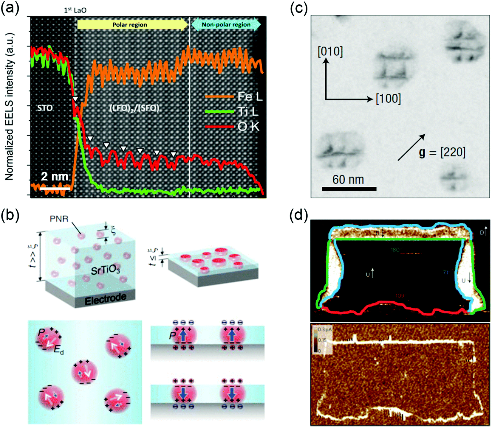 | ||
| Fig. 3 (a) Core-loss EELS of (LaFeO3)2/(SrFeO3) superlattice showing oxygen vacancy ordering (denoted by white arrows) in a polar region. Reproduced with permission.49 Copyright 2014 American Chemical Society. (b) Schematic illustration of the effect of size confinement on polar nanoregions (PNR) induced by non-stoichiometry/Sr-defiency in SrTiO3. Reproduced with permission.9 Copyright 2015 AAAS. (c) Bright-field plan view image recorded under g = [220] on specimens annealed at 950 °C for 1 h, the dark contrasts showing the network of misfit dislocations. Reproduced with permission.59 Copyright 2004 Springer Nature. (d) Conductivity at ferroelectric domain walls: PFM phase image (top) and corresponding conductive-AFM image (bottom) of a written domain pattern in a monodomain (∼100 nm thick) BiFeO3 film, showing all three types of domain wall, that is, 71° (blue), 109° (red) and 180° (green), and showing conduction at both 109° and 180° domain walls and an absence of conduction at the 71° domain walls. Reproduced with permission.15 Copyright 2009 Springer Nature. | ||
The switching between polarized domains in ferroelectric oxides is mediated by nanoscale defects, such as misfit dislocations and grain boundaries.14,59–63 Using in situ transmission electron microscopy, Gao et al. found that misfit dislocations can exert a weak pinning force on domain wall motion in PbZr0.2Ti0.8O3 films.60 Misfit dislocations can also induce polarization instability in PbZr0.52Ti0.48O3 film under compressive strain (Fig. 3c).59 The flexoelectric effect induced polarization in SrTiO3 has been predicted around misfit dislocations at room temperature. Gao et al. directly observed that stable localized electric dipoles exist near the dislocation cores in a 10° small tilt grain boundary in SrTiO3 and further measured the flexoelectric polarization of ∼28 μC cm−2 at the dislocation core.14
When the orientation of electric polarization in ferroelectrics is switched by an applied electric field, this often leads to the appearance of domains of differently oriented regions, separated by domain walls, coexisting in the thin films.64 Such domain walls become more technologically important as the dimensions of individual elements in electronic devices continue to shrink. Recently, a myriad of novel properties and functionalities have been discovered at domain walls in ferroelectric oxide films, such as BiFeO3. One of these intriguing properties is the enhanced conductivity (1 or 2 orders of magnitude higher) at the domain wall compared to the surrounding domains (Fig. 3d).15 The origin of domain wall conductivities is still under debate. The lattice distortion and the consequent band gap lowing of domain walls, and the modification of Schottky barrier heights at the heterojunctions in the regions local to domain walls are the generally accepted mechanisms.15,65–67 In addition, domain walls can accumulate charged defects, such as Fe4+ cations and Bi vacancies in BiFeO3, leading to p-type domain-wall conductivity. An anomalous photovoltaic effect was found at domain walls in BiFeO3 film.67,68 Furthermore, the observed photovoltaic effect can produce voltages that are significantly higher than the bandgap, and electric-field control of domain wall structure allows the photocurrent to be reversed in direction or turn off.67,68
3.2 Magnetism
Magnetic TMOs provide an intellectually rich arena for fundamental scientific discovery and for the invention of faster, smaller, more energy-efficient technologies. VO, VC, grain boundaries, misfit dislocations and BO6 octahedral distortions have been reported as effective methods for changing magnetism. Perovskite manganites of Ln1−xAxMnO3 (Ln = La, Pr, Bi; A = Ba, Sr, Ca) have attracted intensive interest because of the fascinating interplay between spin, charge, orbital and lattice degrees of freedom. The effect of grain boundaries on perovskite manganites has been studied intensively due to its strongly correlation with magnetoresistive (MR) effect.69,70 Gross et al. found that few nm wide grain boundaries of ferromagnetic La2/3Ca1/3MnO3 film becomes paramagnetic (Fig. 4a),12 which strongly modifies the transport properties. Besides, experimental and theoretical calculations have shown that VO can change the hybridized Mn–O–Mn bond and increase the concentration of Mn3+ ions, which affect the double exchange interaction and then modify the magnetic properties.71–73 The transformation from anti-ferromagnetism to ferromagnetism was observed in YMnO3 film by the introduction of VO.73 Li et al. reported that oxygen stoichiometry controls the ferromagnetic insulating state in LaMnO3 film,72 while bulk LaMnO3 shows anti-ferromagnetism. NiO is one of most common natural anti-ferromagnetic oxides the study of which dates back to the dawn of the anti-ferromagnetism.74 To accommodate the ∼7% lattice mismatch between NiO and SrTiO3, high-density dislocations are formed in NiO film grown on a SrTiO3 substrate (Fig. 4b).11,75 O K-edge electron energy-loss spectra (EELS) show that the pre-peak around 528 eV is observed only in the spectrum taken at the dislocation core and is attributed to the formation of Ni deficiency. In turn, ferromagnetic ordering of individual dislocations has been discovered in anti-ferromagnetic NiO films.11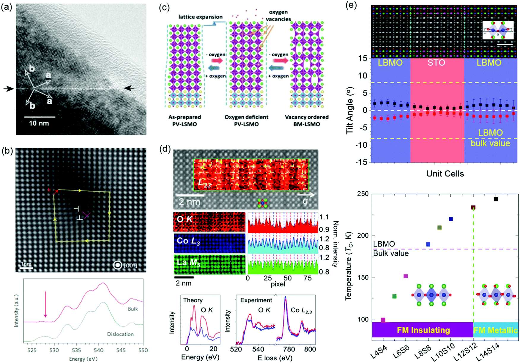 | ||
| Fig. 4 (a) High-resolution transmission electron micrographs of a grain boundary in an epitaxial La2/3Ba1/3MnO3 thin film. The dark and bright arrows mark the grain boundary and the crystallographic axis, respectively. Reproduced with permission.12 Copyright 2000 Elsevier. (b) STEM image of a dislocation core (indicated by the label ⊥ in red) in a NiO thin film. O K-edge EEL spectra measured at the dislocation core and in the bulk region. A peak appears around 526 eV (indicated by the arrow) in the spectrum of the dislocation cores; this is absent in the bulk spectrum. Reproduced with permission.11 Copyright 2013 Springer Nature. (c) A process schematic for lattice expansion and structure transformation from PV to BM induced by reversible oxygen absorption and desorption. Reproduced with permission.78 Copyright 2019 Wiley-VCH. (d) Top: STEM image of LaCoO3 film. Middle: EEL spectra: O K edge, Co L3 edge, and La M5 edge. Bottom: Theoretical O K absorption edge along with experimental O K and Co L2,3 edges for the fully oxygenated CoO2 planes (red) and the O-deficient planes (blue). Reproduced with permission.87 Copyright 2012 American Physcial Society. (e) Top: Integrated differential phase-contrast (iDPC) STEM image of (La0.9Ba0.1MnO3)8uc/(SrTiO3)8uc (LBMO/STO) superlattice. Middle: plane-averaged octahedral tilt angles of LBMO and STO. Bottom: Ferromagnetic insulating (FMI) state to ferromagnetic metallic (FMM) state transition accompanied by the change of MnO6 octahedral rotations. Reproduced with permission.379 Copyright 2020 Wiley-VCH. | ||
A layered vacancy ordered brownmillerite (BM) structure can be topotactically transformed from a perovskite structure framework, in which one-sixth of the oxygen anions have been removed. The special feature of this structure-type provides a new pathway for modifying electronic structure (the hybridization between O 2p and TM d orbitals) and then tuning physical properties (magnetic, transport and optical properties) in TMO films.76,77 Using real-time X-ray diffraction, Cao et al. found the VO-induced topotactic transition from perovskite (ferromagnetic metal) to BM (anti-ferromagnetic insulator) and vice versa in La0.7Sr0.3MnO3 films (Fig. 4c).78 During the topotactic phase conversion, an intermediate phase (La0.7Sr0.3MnO2.65) was also discovered. A similar topotactic phase transformation has also been observed in SrCoOx, SrFeOx, LaCoOx, and SrCrOx films.76,77,79–81 For example, SrCoOx can experience a phase transition from the perovskite SrCoO3 (P-SCO) to brownmillerite SrCoO2.5 (BM-SCO) with an increase of VO concentration.76 Magnetic properties are simultaneously altered with an increase of VO concentration due to the change of Co valency, from ferromagnetic P-SCO to antiferromagnetic BM-SCO.82
Epitaxial strain, caused by lattice mismatch between the film and substrate, can enhance or suppress the diverse properties of TMO films. To accommodate the lattice mismatch, long-range defect ordering, e.g. VO, can be formed.83,84 Coupling between strain and VO has been widely studied in LaCoO3 films, where long-range ferromagnetic ordering is observed, while bulk LaCoO3 shows no magnetism at low temperature.85–88 Dark stripes in Z-contrast STEM images have been observed in ferromagnetic LaCoO3 films grown on SrTiO3 substrates (Fig. 4d).87 Biskup et al. attributed these stripes to VO ordering, where the dark strips are ferromagnetic insulating regions and significant oxygen deficiency results in the lattice relaxation. This conclusion is based on the fact that there is no significant stoichiometry change for La and Co elements, and there are remarkably reduced O peak intensities in the striped regions observed in atomically resolved electron energy-loss spectroscopy (EELS). However, Choi et al. also reported the dark stripes in Z-contrast STEM images of LaCoO3 films grown on the SrTiO3 substrates and proposed that dark stripes originate from the modulation of the atomic arrangement, caused by the ferroelastic nature of the system, instead of VO ordering. This conclusion is obtained from there being no significant change in the oxygen non-stoichiometry observed in X-ray absorption spectroscopy.86 Up to now, it is still not clear whether the ferromagnetism in LaCoO3 film is caused by strain-induced VO ordering or by strain-induced lattice modulation. When Sr is doped to LaCoO3, VO are created to neutralize the charge difference between La and Sr. Consequently, dark stripes were observed in La0.5Sr0.5CoO3 films and certainly originated from the formation of VO ordering.83
The fascinating properties of perovskite TMOs are essentially determined by the interlinked and corner-connected BO6 octahedra, whose bond lengths and bond angles determine the hybridization between TM d and oxygen 2p orbitals, significantly altering the interplay between spin, charge, orbital and lattice degrees of freedom.89–91 Tuning of the BO6 octahedra has been widely studied by strain engineering, which changes the c/a ratio for achieving the orbital reconstruction. Using X-ray linear dichroism, Pesquera et al. investigated the orbital reconstruction and the symmetry breaking effect in La2/3Sr1/3MnO3 films and found that the eg electrons of thick La2/3Sr1/3MnO3 films prefer the d3z2−r2 orbitals under compressive strain and the dx2−y2 orbitals under tensile strain.92 In the case of (La2/3Sr1/3MnO3)n/(BaTiO3)n superlattice films, through strain engineering and a carefully designed superlattice geometry, the interfacial Mn cations favor the d3z2−r2 orbitals with c/a > 1 while the dx2−y2 orbitals are stabilized for the inner Mn cations, resulting in an enhancement of ferromagnetic Curie temperature.93 On the other hand, recent studies demonstrated that oxygen octahedral coupling (OOC) at the hetero-interfaces can delicately tailor the local BO6 octahedral rotations at an atomic-scale.94–98,379 Zhai et al. studied the (LaMnO3)n/(SrTiO3)m superlattices and found that the magnitude of ferromagnetic magnetization is strongly correlated with MnO6 octahedral rotations.99 A modulation of the emergent interfacial ferromagnetism was realized in (CaRuO3)n/(CaMnO3)m superlattices, comprised of an anti-ferromagnet and a paramagnet, through controlling the rotation patterns.100 The magnetic anisotropy of La2/3Sr1/3MnO3 and SrRuO3 films can also be controlled by engineering the MnO6 and RuO6 octahedral rotations,101,102 respectively. It should be noted that the epitaxial strain also changes the BO6 octahedral rotations in TMO films.103 To minimize the strain effect on the changes of BO6 octahedral rotations and to understand the correlation between the BO6 octahedral rotations, electronic structure and physical properties in TMO films, Li et al. studied (La0.9Ba0.1MnO3)n/(SrTiO3)n (only ∼0.26% lattice mismatch) superlattices and achieved a long range (up to 12 unit cells) suppression of the MnO6 octahedral rotations, a preferential occupation of the out-of-plane Mn d3z2−r2 orbital and a reduced Mn eg bandwidth in La0.9Ba0.1MnO3. Consequently, a new ferromagnetic insulating state with enhanced Curie temperature of 235 K emerges in La0.9Ba0.1MnO3 (Fig. 4e).379
3.3 Multi-ferroelectricity and dielectricity
The ability of multiferroic materials to couple magnetic and ferroelectric orders continues to attract intensive interest because of their potential applications in sensors, spintronics and memory devices.104–108 Such materials are, however, rare as a consequence of the competing requirements for ferroelectricity and magnetism.109 Multi-ferroelectricity can be modified or created by domain walls, misfit dislocations, VO and atomic displacements. Until recently BiFeO3 was the only materials with this functionality at room temperature.110,111 To relax the misfit strain associated with the lattice mismatch between the BiFeO3 film and the substrate, the formation of crystallographic defects, such as domain walls and dislocations, might occur. Domain walls in multiferroics can manifest a net magnetic moment even if the domains themselves are anti-ferromagnetic or paramagnetic.112 He et al. reported a strong magnetoresistance in domain walls of BiFeO3 films grown on DyScO3 substrates.113 Edge dislocations in BiFeO3 films have been observed by scanning transmission electron microscopy.114 Agrawal et al. found the presence of Bi and Fe atoms in dislocation cores which result in uncompensated Fe spins along the dislocations and give rise to a magnetic signal in BiFeO3 film.115In VO-ordered brownmillerite SrFeO2.5 (anti-ferromagnetic insulator), by controlling the 1D FeO4 tetrahedral chain network, Kang et al. reported the realization of a room-temperature ferroelectric ferromagnetic in SrFeO2.5 film.116 Li et al. demonstrated that VO create Ti3+ 3d1 defect states, mediating the ferromagnetic coupling between the localized Eu 4f7 spins, and an increase in the off-center displacement of Ti ions, enhancing the ferroelectric Curie temperature in Eu0.5Ba0.5TiO3−δ film.117,118 Similar achievements of ferroelectricity and ferromagnetism was also observed in YMnO3 films by the manipulation of VO.73
Engineering specific atomic displacements or geometric design has been applied to design a single-phase multiferroic. Hexagonal LuFeO3 is a geometric ferroelectric with the greatest known planar rumpling.119 In the (LuFeO3)m/(LuFe2O4)1 superlattices, Mundy et al. introduced the individual monolayers of FeO during the growth to construct formula-unit-thick layers of ferromagnetic LuFe2O4 within the LuFeO3 matrix and further demonstrated that the severe rumpling imposed by the neighbouring LuFeO3 enhances the magnetic transition temperature of LuFe2O4 to 281 K and also drives LuFe2O4 into a ferroelectric state (Fig. 5a).120 Moreover, electric-field control of magnetism has been realized at 200 K. Through the engineering of octahedral tilts, room-temperature ferroelectric ferromagnetic and magnetoelectric coupling have been realized in (CaySr1−y)1.15Tb1.85Fe2O7.121 Choi et al. and Chen et al. reported room-temperature multiferroic films based on two partially miscible phases of BiFeO3 and BiMnO3.122,123
 | ||
| Fig. 5 (a) HAADF STEM images of top: end-members LuFe2O4 (left) and LuFeO3 (right); middle: (LuFeO3)9/(LuFe2O4)1 superlattice film. Bottom left: Loops of the magnetization as a function of the magnetic field for the (LuFeO3)9/(LuFe2O4)1 superlattice. Bottom right: Out-of-plane PFM image of the (LuFeO3)9/(LuFe2O4)1 superlattice. Reproduced with permission.120 Copyright 2016 Springer Nature. (b) Bright-field STEM image of epitaxial Srn+1TinO3n+1 (n = 6) film grown on DyScO3. The ratio of K11 under an applied bias field (Ebias) to that at zero bias field (left-hand axis) and tunability (right-hand axis) of the n = 6 sample at several different frequencies in the microwave range. The inset shows the dielectric constant ratio as a function of frequency for several values of applied Ebias. Reproduced with permission.126 Copyright 2013 Springer Nature. (c) Top: A cross-sectional TEM image of a BFO:SmO VAN film with vertical nanocolumns of BFO and SmO (B represents BFO, and S represents Sm2O3) Middle: Frequency-dependent dielectric constant and dielectric loss of BFO:SmO VAN thin films, compared to BFO and SmO single-phase thin films. Bottom: Leakage current density versus electric field (J–E) characteristics of BFO:SmO, BFO, and SmO thin films. Reproduced with permission.129 Copyright 2009 Wiley-VCH. | ||
Dielectric materials exhibiting temperature- and frequency-stable permittivity as well as dielectric tunability and sufficiently low dielectric loss, continues to arouse considerable interest motivated by their myriad device miniaturization and high-energy-density storage application.124,125 Dielectricity can be tuned by VO, VC, misfit dislocations and dipolar defects. Lee et al. demonstrated that the presence of (SrO)2 crystallographic shear planes in Srn+1TinO3n+1 film provides a means of locally accommodating non-stoichiometry (Sr vacancies), which significantly reduces the dielectric loss and achieves the dielectric tunability (20% at 50 kV cm−1) across the entire microwave range (Fig. 5b).126 Vertically aligned nanocomposites (VANs) with ordered vertical heterointerfaces provide an effective platform to tune the dielectric properties. Lee et al. studied the dielectric tunability in Ba0.6Sr0.4TiO3:Sm2O3 VAN films and reported the achievement of a low dielectric loss (tan![[thin space (1/6-em)]](https://www.rsc.org/images/entities/char_2009.gif) δ < 0.1) and high and stable dielectric tunability (75% at 200 kV cm−1) at room temperature.127 A very low dielectric loss (tanδ ∼ 0.01) and relative large dielectric tunability (49% at 400 kV cm−1) was further reported in SrTiO3:Sm2O3 VAN film.128 Yang et al. explored BiFeO3:Sm2O3 VAN films and found that dielectric loss and leakage current were reduced compared to plain BiFeO3 films (Fig. 5c).129,130 The increased vertical interfacial area and reduced VO in the BiFeO3 phase are responsible for these improved properties. Enhanced ferroelectric Curie temperatures and reduced leakage current were also reported in BaTiO3:Sm2O3 VAN films.131,132 Li et al. found that the misfit dislocations are formed at the vertical interface due to a large vertical lattice strain. The movement of VO is confined at the vertical interface and hampered by the misfit dislocations, which contributed to a relaxation behavior in BaTiO3:Sm2O3 VAN film.133 Dipolar defects are created by the change of VO concentration and further interact with the off-centered Ti ions, which results in dielectric relaxation in Eu0.5Ba0.5TiO3−δ films.134
δ < 0.1) and high and stable dielectric tunability (75% at 200 kV cm−1) at room temperature.127 A very low dielectric loss (tanδ ∼ 0.01) and relative large dielectric tunability (49% at 400 kV cm−1) was further reported in SrTiO3:Sm2O3 VAN film.128 Yang et al. explored BiFeO3:Sm2O3 VAN films and found that dielectric loss and leakage current were reduced compared to plain BiFeO3 films (Fig. 5c).129,130 The increased vertical interfacial area and reduced VO in the BiFeO3 phase are responsible for these improved properties. Enhanced ferroelectric Curie temperatures and reduced leakage current were also reported in BaTiO3:Sm2O3 VAN films.131,132 Li et al. found that the misfit dislocations are formed at the vertical interface due to a large vertical lattice strain. The movement of VO is confined at the vertical interface and hampered by the misfit dislocations, which contributed to a relaxation behavior in BaTiO3:Sm2O3 VAN film.133 Dipolar defects are created by the change of VO concentration and further interact with the off-centered Ti ions, which results in dielectric relaxation in Eu0.5Ba0.5TiO3−δ films.134
3.4 2DEG and 2DHG
The emergence of conducting interface can be promoted by polar discontinuities. Ohtomo et al. reported the discovery of a two-dimensional electron gas (2DEG) at the LaAlO3/SrTiO3 heterostructures based on this idea.135 Both compounds are band insulators (Egap = 5.6 eV for bulk LaAlO3 and Egap = 3.2 eV for bulk SrTiO3). However, when a LaAlO3 layer is deposited layer-by-layer on top of a (001) TiO2-terminated SrTiO3 substrate, the interface switches to a metallic state when the LaAlO3 layer thickness exceeds 3 unit cells.136 These experimental observations have generated a lot of interest in the SrTiO3-based interfaces,137,138 due to their potential applications in novel electronic devices and rich physics arising from the complex electronic correlations.139–141 Although significant attempts have been paid to understand the LaAlO3/SrTiO3 interface, the origin of interfacial conductivity is still under debate. From the very beginning, the conductivity observed at the LaAlO3/SrTiO3 interface was attributed to the polar discontinuity.135 This polar catastrophe scenario emerges from a simple valence counting consideration. As shown in Fig. 6a, the TiO2 and SrO planes are neutral, however, the LaO and AlO2 layers are polar and carry a positive and negative charge of +1 e and −1 e per unit cell, respectively. The diverging electric potential can be compensated by electron transfer from LaAlO3 to the interfacial SrTiO3 layer with the formation of the n-type interface. The polar catastrophe picture explains many of the features of the electron gas at the LaAlO3/SrTiO3 interface, in particular the existence of a critical thickness for the onset of metallic behavior. However, some unresolved inconsistencies between theories and experiments still exist. For example, the predicted sheet carrier densities and their variation with LaAlO3 thickness have not been observed in experiments yet.136,142 | ||
| Fig. 6 (a) Sketch of two mechanisms, polar discontinuity and oxygen vacancies, for inducing mobile electrons at the LaAlO3/SrTiO3 interface. Reproduced with permission.3,378 Copyright 2018 Wiley-VCH and Copyright 2013 American Physcial Society. (b) Temperature-dependent sheet resistance Rxx for the interface between LaAlO3 and SrTiO3. Reproduced with permission.135 Copyright 2004 Springer Nature. (c) AlO2/LaO/TiO2 interface showing the fractions of elemental Ti and La from the Ti-L and La-M edges, as well as the Ti3+ fraction determined from a least-squares fit to the Ti-L edge from Ti3+ and Ti4+ reference spectra. There is excess Ti3+ on the substrate side of the interface. Reproduced with permission.149 Copyright 2006 Springer Nature. (d) Left: Schematics that depict the electronic reconstruction across the oxide heterostructure. Right: Hall resistance Rxyversus magnetic field μ0H for the top and bottom interfaces at 4 K. The top interface clearly shows a positive slope, which indicates p-type conductivity, whereas the bottom interface shows a negative slope, which indicates n-type conductivity. Reproduced with permission.150 Copyright 2018 Springer Nature. | ||
Besides the polar discontinuity, the defects (e.g., VO) and cation intermixing are also invoked to understand interfacial conductivity.143,144 It was found that charge transport depends sensitively on the growth conditions, especially on the oxygen pressure PO2, indicating that VO could be an alternative doping mechanism.135,145–147 Temperature-dependent sheet resistance Rsheet depends dramatically on the growth pressure (Fig. 6b). For PO2 ∼ 10−6 mbar, the observation of a larger carrier density originates from the doping of VO to the SrTiO3 substrate. For PO2 between 10−4 and 10−2 mbar, the observation of conductivity is believed to be confined to the interface. When the PO2 is above 10−2 mbar, the reported results are more diversified, such as insulating, superconducting and magnetoresistance effects.147,148 Atomic-resolution electron energy loss spectroscopy (EELS) revealed that the interface is not chemically sharp, with some La/Sr and Ti/Al intermixing included (Fig. 6c).149 Such chemical doping could also be the source of the carriers at the interface, with the interface layer behaving as a La1−xSrxTiO3 film, which are responsible for the interfacial conductivity. Recently, Lee et al. reported the observation of a two-dimensional hole gas (2DHG) in (001) SrTiO3/LaAlO3/SrTiO3 heterostructures (Fig. 6d).150 The SrTiO3 substrate is terminated at TiO2. Depth-resolved cathodoluminescence spectroscopy (DR-CLS) was used to support that the formation of 2DHG is not attributed to the VO.
The fundamental questions on the origin of the carrier, the carrier density, the shape of the confining potential and the role of electronic correlations are too complicated and still can’t be answered at the LaAlO3/SrTiO3 interface and other similar systems. More comprehensive discussions can be found in other review papers.3,151–153
3.5 Metal–insulator transitions
Understanding metal–insulator transitions in strongly correlated materials is one of the major challenges in condensed matter physics,154–158 with implications for both fundamental science and technology.159,160 Strain, VO and BO6 octahedral distortions have been applied for manipulating metal–insulator transition behaviour. An archetypal correlated material is VO2, showing a pronounced metal–insulator behavior from low-temperature insulating monoclinic (M1) phase to high-temperature metallic rutile (R) phase near room temperature (341 K in bulk).161 Epitaxial strain and VO defects have been widely used in order to control metal–insulator transition dynamics for achieving a shape phase transition in VO2 epitaxial films.162–166 Using electrolyte gating with an ionic liquid, Jeong et al. reported that the suppression of the metal–insulator transition in VO2 film is achieved by electric field-induced VO formation for reducing the valence state of V4+ to V3+ (Fig. 7a).167 However, creation of VO by ionic liquid gating is possibly linked with both hydrogen intercalation whence a trace of water remains in the ionic liquid and degradation of the entire film under high electric field.164,168 By growing the VO2−δ/VO2 bilayer films on TiO2 substrates, Lee et al. found that an interface interaction between VO2−δ and VO2 can suppress the electronic correlations for controlling the metal–insulator transition.169 By annealing VO2 films at an ultralow oxygen partial pressure (PO2 ∼ 10−24 atm), the formation of VO led to a change of the band structure (Fig. 7b) and an appearance of a metallic state down to 1.8 K.165 Moreover, the VO2 film can revert back to its original state by a simple annealing process in oxygen. | ||
| Fig. 7 (a) Sheet resistance versus temperature for various gate voltages varying from 0 to 1.8 V for VO2/(001)TiO2. Reproduced with permission.167 Copyright 2013 AAAS. (b) Schematic illustration of the band structure of pristine VO2 in the insulating state (top) and metallic state (bottom left), while the band structure of oxygen-deficient VO2−δ is shown in bottom right, where strong charge filling in the π* and d‖ orbitals occurs. Reproduced with permission.165 Copyright 2017 American Physical Society. (c) Temperature-dependent resistivity of (LaFeO3)1–(SmNiO3)n superlattices and 30 uc SmNiO3 film. Reproduced with permission.183 Copyright 2018 National Academy of Sciences. | ||
As discussed above, during the transformation of a layered VO ordered brownmillerite structure to a perovskite structure framework, the modification of electronic structure, such as the hybridization between O 2p and TM d orbitals, is responsible for the reversible change between the brownmillerite insulating state and the perovskite metallic state. This phenomenon has been widely observed in La0.7Sr0.3MnO3−x, SrCoOx, SrFeOx, LaCoOx, and SrCrOx films.76–81 Taking SrFeOx as an example, SrFeO2.5 exhibits insulating (or semiconducting) behaviour in the BM structure while SrFeO3 shows metallic behaviour in the perovskite structure. By using different growth atmospheres (oxygen partial pressure) or by modifying the interfacial strain by changing the growth substrates, VO concentration could be successfully controlled and could therefore modulate the conductivity and metal–insulator transition.81,170
The properties of perovskite rare-earth nickelates, RNiO3 (R = La–Lu), have been attracting enormous attention owing to a rich temperature-composition phase diagram including a metal-to-insulator phase transition coinciding with a nickel charge ordering.16,171,172 The origin of the metal-to-insulator transition has been widely debated in the literatures.173–176 The unoccupied states at the bottom of the conduction band have substantial oxygen character, corresponding to an oxygen ligand hole consistent with a negative charge transfer character for the system.177 In a non-disproportionated structure, the nickel sites have nominal valence 3+ and the oxygen ligand holes are distributed equally among all of the NiO6 octahedra, resulting in a d8![[L with combining low line]](https://www.rsc.org/images/entities/char_004c_0332.gif) configuration, where denotes an oxygen ligand hole. VO in the rare-earth nickelates can modify the electronic structure and act as electron donors. The added electron can be regarded as converting nickel from 3+ to 2+, or as converting the nickel site in the NiO6 octahedron from d8 to d8. This results in a large on-site bandgap stemming from the electron–electron correlations and the crystal field splitting. As a result, metal–insulator transitions of LaNiO3, NdNiO3 and SmNiO3 films can be controlled by the formation of VO.178–181 Recently, Mercy et al. identified that the breathing mode responsible for the metal–insulator transition in the perovskite nickelates is triggered by NiO6 octahedral rotations and tilts.182 Based on this idea, in the case of the (LaFeO3)1/(SmNiO3)n superlattices, Liao et al. demonstrated that the metal–insulator transition in the SmNiO3 layer can be adjusted by the modulation of NiO6 octahedral tilt (Fig. 7c).183
configuration, where denotes an oxygen ligand hole. VO in the rare-earth nickelates can modify the electronic structure and act as electron donors. The added electron can be regarded as converting nickel from 3+ to 2+, or as converting the nickel site in the NiO6 octahedron from d8 to d8. This results in a large on-site bandgap stemming from the electron–electron correlations and the crystal field splitting. As a result, metal–insulator transitions of LaNiO3, NdNiO3 and SmNiO3 films can be controlled by the formation of VO.178–181 Recently, Mercy et al. identified that the breathing mode responsible for the metal–insulator transition in the perovskite nickelates is triggered by NiO6 octahedral rotations and tilts.182 Based on this idea, in the case of the (LaFeO3)1/(SmNiO3)n superlattices, Liao et al. demonstrated that the metal–insulator transition in the SmNiO3 layer can be adjusted by the modulation of NiO6 octahedral tilt (Fig. 7c).183
3.6 Resistive switching
Resistive random-access memory (RRAM or ReRAM) is one of the most promising emerging devices for logic-in-memory operations, attracting great attention due to the possibility of high-density integration, plausible scalability, ultra-fast access time, low power consumption and ease of fabrication. ReRAMs can be divided into two categories: electrochemical metallization cells ReRAMs – also called conductive bridge random access memories – and valence change mechanism ReRAMs – also called redox random access memories ReRAMs.184,185 Resistive switching behaviour can be manipulated by controlling cations, VO and interfaces. In electrochemical metallization cells, a nanoscale conductive metallic path between a working electrode/anode (often electrochemically active, such as Ag or Cu) and a counter electrode/cathode (often inert, such as Pt, Au or TiN) is formed or broken by the generation, movement and reduction of mobile metal cations (i.e., Ag+ or Cu2+).186,187 Valence change mechanisms occur in a wide range of TMOs.188,189 In TMOs, anions such as oxygen ions (or, equivalently, VO) are more mobile than the cations when they are thermally and/or electrically activated. Therefore, understanding how the resistance of TMOs is influenced by VO is very important. Generally, VO will affect the resistance and contribute toward the introduction of resistive switching phenomena in one of three ways: (1) VO tend to cluster and generally form filamentary shapes under an electric field (Fig. 8a).190–192 When such clusters are formed, the resistance of the local region becomes much lower than that of the surrounding oxide matrix, and the low-resistance state (LRS) and high-resistance state (HRS) will therefore be determined by the creation and rupture of the conducting filaments (CFs), respectively. (2) VO can control the Schottky barrier characteristics.188,193 In a typical capacitor sample geometry, an interface is formed between the metal electrode and the TMOs films. Depending on the difference of work functions between the metal electrode and the TMOs, a Schottky barrier can be formed. Under an external bias, the distribution and density of VO can vary, which affects the height and width of the Schottky barrier and leads to a change in the resistance of the sample. (3) VO can also form trap sites for electrons inside the Schottky barrier region.193–195 In this situation, the Schottky barrier can be modulated by the neutralization of the VO due to the trapping of electrons, inducing resistive switching phenomena.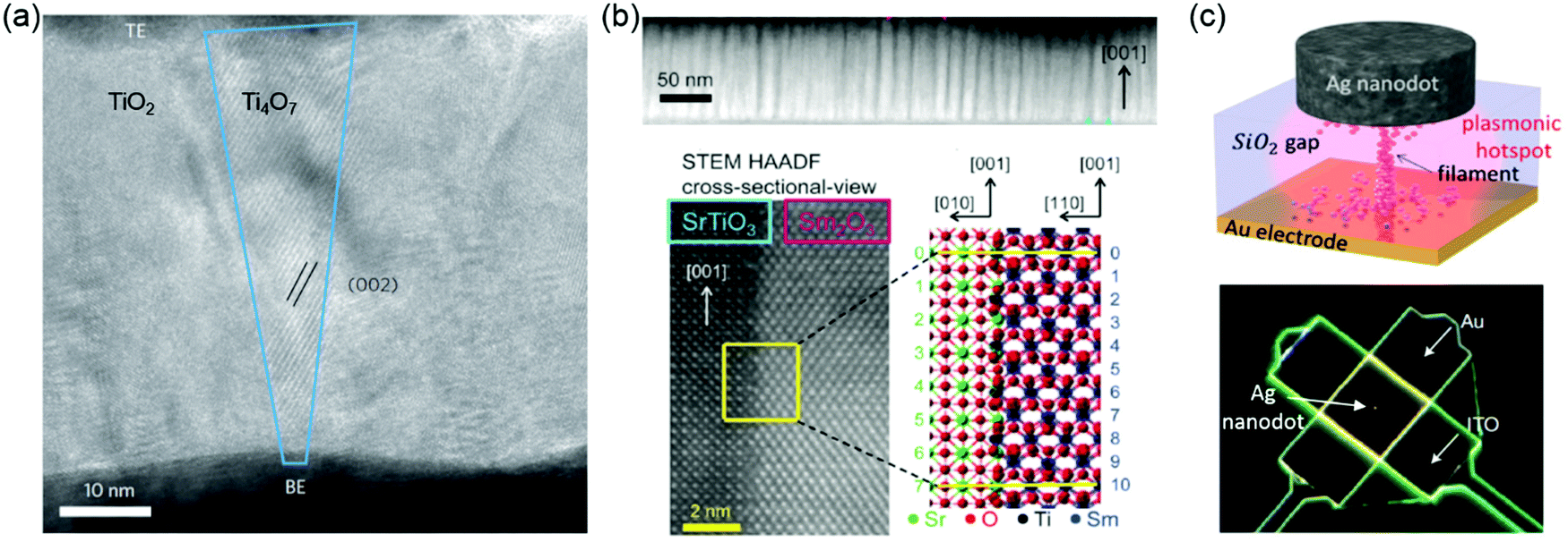 | ||
| Fig. 8 (a) High-resolution transmission electron microscopy (HRTEM) image of a nanocrystalline Ti4O7 (Magnéli phase) filament with a conical shape (outlined in blue) in a Pt/TiO2/Pt anion-type RSM device. Reproduced with permission.190 Copyright 2010 Springer Nature. (b) Top: Spontaneous phase ordering of SrTiO3 and Sm2O3 in a cross-sectional TEM image. Bottom: HRTEM image of the vertical interface between a SrTiO3 matrix and Sm2O3 nanocolumn. Atomic arrangement at the vertical interface can be crystallographically modelled. Reproduced with permission.196 Copyright 2014 Wiley-VCH. (c) Sketch (top) and SEM (bottom) image of a nanoparticle-on-mirror (NPoM) memristive cell. Reproduced with permission.198 Copyright 2016 Wiley-VCH. | ||
Resistive switching devices are normally in the form of metal-dielectric-metal two-terminal junctions. The interface between metal electrode and the TMOs films plays a critical role in the resistive switching. Using vertical heterointerfaces in vertically aligned nanocomposite (VAN) films for studying resistive switching has been reported. Different from lateral heterostructures, VANs exhibit a much higher density of vertical interfaces which can be used for improving resistive switching. Lee et al. reported that due to the structural incompatibility of SrTiO3 and Sm2O3, the possible formation of VO was found at vertical heterointerfaces.196 The Joule heating-accelerated drift of VO localized at vertical heterointerfaces reduces the wide fluctuation in switching parameters (Fig. 8b). In self-assembled Sm-doped CeO2 and SrTiO3 VAN films, large on–off ratios and high reproducibility were achieved by the separate tailoring of nanoscale ionic and electronic channels.197
Although great progresses have been made in valence change mechanism ReRAMs, mastery of the conduction mechanism is still incomplete. To identify and understand failure mechanisms, characterization methods, such as voltage-sweep and voltage-pulse measurements, electrochemical cyclic voltammetry, and ex situ and in situ electron microscopy have been used. However, limited success is achieved in fully understanding the switching dynamics. Recently, a spectroscopic technique to optically characterize in situ resistive switching effect was reported.198 Resistive switches arranged in a nanoparticle-on-mirror (NPoM) geometry were developed, exploiting the high sensitivity to morphological changes occurring in the tightly confined plasmonic hotspot within the switching materials (Fig. 8c).198 This provides a non-destructive technique to understand the switching dynamics.
Recently published reviews provide more comprehensive discussions on classification of resistive switching phenomena/mechanisms, other microscopic origins of resistive switching in TMOs, resistive switching related technological issues (e.g., fluctuation, sneak-paths and multilevel switching) and neuromorphic computing based on resistive switching which has drawn extensive attention due to its promising capability in processing massive data in the Internet of Things and big-data workloads.199–203
3.7 Ionic conductivity
One of the leading technologies for future power generation is the solid oxide fuel cell (SOFC).204–206 One important challenge in improving SOFC technology is to reduce the working temperature to 500–700 °C. Over several decades, developing new electrolyte materials with high ion conductivity has been the primary activity. The oxygen diffusivity (D) scales almost linearly with VO concentration when the value of VO is low. On the other hand, oxygen diffusion is a thermally activated process where D can be described by the Boltzmann relationship as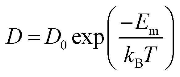 , where D0 is a constant and Em denotes migration enthalpies or energy barrier along this path. Compared to linear relationship between D and VO concentration, D changes exponentially with Em which makes it a critical parameter to reduce.206 The oxygen migration energy can be modified by misfit dislocations, VO, elastic strain, BO6 octahedral distortion, and so on.
Yttria-stabilized zirconia (YSZ) is the material mostly used in SOFCs because of its mechanical stability, chemical compatibility with electrodes, and high oxygen ionic conductivity. Engineering misfit dislocation and VO at heterogeneous interfaces have been used to improve the charge-carrier density and enhance the ionic conductivity. For example, Garcia-Barriocannal et al. reported an eight-orders-of-magnitude enhancement of YSZ conductivity in epitaxial multilayers consisting of two unit cell YSZ and thick SrTiO3, which attributes colossal enhancement of ionic conductivity to either VO or O disorder in the interfacial plane.207 Density-functional calculations revealed that colossal ionic conductivity in YSZ/SrTiO3 multilayers can be explained in terms of lattice-mismatch strain and O-sublattice incompatibility at the interface (Fig. 9a).208 However, these experimental results still have to be independently verified, as there are some debates as to whether the conductivity of YSZ/SrTiO3 multilayers is purely ionic.209 Sillassen et al. reported that interfacial effects dominate the conductivity at the low temperature (<350 °C), showing more than three orders of magnitude enhancement in YSZ films compared to bulk YSZ.210 The observed enhancement in lateral ionic conductivity is caused by a combination of misfit dislocations and elastic strain at the interface (Fig. 9b and c). Similar evidences for misfit dislocations related to fast ion conduction in lateral heterostructures are reported in numerous experimental and theoretical studies.211–215
 | ||
| Fig. 9 (a) Structure of the 1 nm YSZ layer sandwiched between layers of STO at 360 K. Sr atoms are shown as large yellow balls, Ti in blue, Zr in green, Y in gray, and O in red. Reproduced with permission.208 Copyright 2010 American Physical Society. (b) HRTEM image of the YSZ/MgO interface region. The inset shows the SAED pattern across the YSZ/MgO interface along the YSZ (100) direction. Reproduced with permission.210 Copyright 2010 Wiley-VCH. (c) Magnification of the area marked in (b). Misfit dislocations are indicated by T symbols. (d) Ionic conductivity of plain YSZ films compared to YSZ-STO VAN films. Reproduced with permission.218 Copyright 2015 American Chemical Society. (e) Ionic conductivity as a function of unit-cell volume and octahedral rotation angles for LSGM. Reproduced with permission.220 Copyright 2020 Wiley-VCH. | ||
Vertically aligned nanocomposite (VAN) films have been also developed to improve the ionic conductivity and design state-of-the-art ionic devices.216,217 Compared to the oxygen ion diffusion along lateral interface direction in the lateral heterostructures, VANs allow fast oxygen ion transport along the out-of-plane direction which is the favored charge flow direction of SOFCs. Enhanced ionic conductivity values by over 2 orders of magnitude, compared to plain YSZ films, was reported in YSZ:SrTiO3 VAN films (Fig. 9d).218 The improved crystallinity of YSZ nanocolumns in VAN film was proposed to explain the enhanced ionic conductivity. Similar to YSZ:SrTiO3 VAN films, the enhancement in vertical ionic conductivity has been also demonstrated in VAN systems of YSZ:GDC218 (Gd-doped CeO2) and SrTiO3:SDC (Sm-doped CeO2).219
Very recently, Gao et al. reported that, through the creation of La0.9Sr0.1Ga0.95Mg0.05O3−δ/DyScO3 superlattice films, both expanded unit-cell volume and large octahedral rotations can be realized in La0.9Sr0.1Ga0.95Mg0.05O3−δ (LSGM), which shows an enhancement of ionic conductivity (Fig. 9e).220 This provides a new pathway for the rational design of ion-conducting perovskite electrolytes via controlling BO6 octahedral rotations.
3.8 Photo-electrocatalyst and electrocatalysts
Electrochemical water splitting to produce storable hydrogen (also referred to as “solar fuel’’) driven by solar energy or by electricity from renewable energy (e.g., photovoltaics) is widely seen as a promising pathway towards a globally sustainable energy future. The key to enabling these approaches is the development of abundant, low-cost, stable semiconductor materials to harness solar energy and efficient electrocatalysts to accelerate the water oxidization reaction.221 Complex TMOs are appealing materials for these purposes, owing to their earth-abundance, good stability and tunable physicochemical properties via doping and defect engineering (especially VO, VC and lattice distortions).222–224To achieve effective implementation of solar driven photoelectrochemical water splitting (PEC), stringent requirements on the material properties should be satisfied, including an appropriate bandgap for sufficient light absorption, adequate band edge potentials to drive redox reactions, favorable carrier diffusion length to ensure the effective progress of the interface reaction. TMO semiconductors such as TiO2, Fe2O3 and BiVO4 have attracted intensive attention for the last decades.225–228 However, their PEC performance is still far from the standard of practical applications, because of limitations in materials properties. For example, TiO2 has a much too large bandgap (3.0–3.2 eV) for visible light absorption.229,230 Fe2O3 has a low bandgap of ∼ 2.1 eV, but is inherently limited by its low electrical conductivity, short diffusion length (2–4 nm) and lifetime (<10 ps) of photoexcited carriers.231,232
Doping, alloying and defect engineering are widely used as strategies to enhance the PEC activity with the purpose of: (i) decreasing the bandgap for efficient visible light absorption and (ii) optimizing the carrier transport. Doping can introduce extra energy levels within the bandgap (for example, Bi3+ 6s2 state hybrid with Ti4+ d0 orbital) to narrow the bandgap value.233 On the other hand, it has been shown that Fe2O3 can be p-type doped by divalent cations such as Mg2+,234,235 and n-type doped with tetravalent cations such as Ti4+, Sn4+, etc.236–239 Doped Fe2O3 can remarkably enhance the PEC activity toward water oxidation compared with undoped counterparts.239–242 The same trend of enhanced PEC activity was also achieved in Mo6+ or W6+ doped BiVO4.243–246
Defect engineering is another approach to tuning the band structure and therefore PEC performance of TMOs, especially VO, VC, and lattice distortion. VO provide donor states to increase n-type conductivity, while VC provide acceptor states for p-type conductivity.247,248 Furthermore, the defects also provide favorable absorption sites for chemical reactions to enhance the activity. Cui et al. prepared black TiO2 nanotubes (B-TNTs) with abundant VOvia the Al reduction method, which shows 5 times higher applied bias photon-to-current efficiency (ABPE) than that of TNTs and a larger visible light photoresponse region from 400 nm to 460 nm.249 The new donor level at about 0.7 eV below the conduction band minimum (CBM) corresponding to the formation of VO.250 Yim and coworkers attribute the bandgap state in TiO2 (110) to bridging VO by ultraviolet photoemission spectroscopy and scanning tunneling microscopy.251 But the contribution of interstitial Ti is also proposed in another work.252 Because of the increased carrier density and the lowered activation energy for charge transport, the separation and migration of photo-excited carriers can be effectively improved. However, excess VO may trap photoelectrons and act as recombination centers, and then decrease the photocurrent.253 The above effects also hold for BiVO4.254,255
Furthermore, the presence of VO has the ability to work as active site for PEC water splitting and enhance the adsorption energies of H2Oads, OHads, and Oads (Fig. 10a).256 The strong interaction indicates that an increased overlap between Bi 6s, V 3d and O 2p orbitals, and then accelerates the hole transfer at electrode/electrolyte interface.
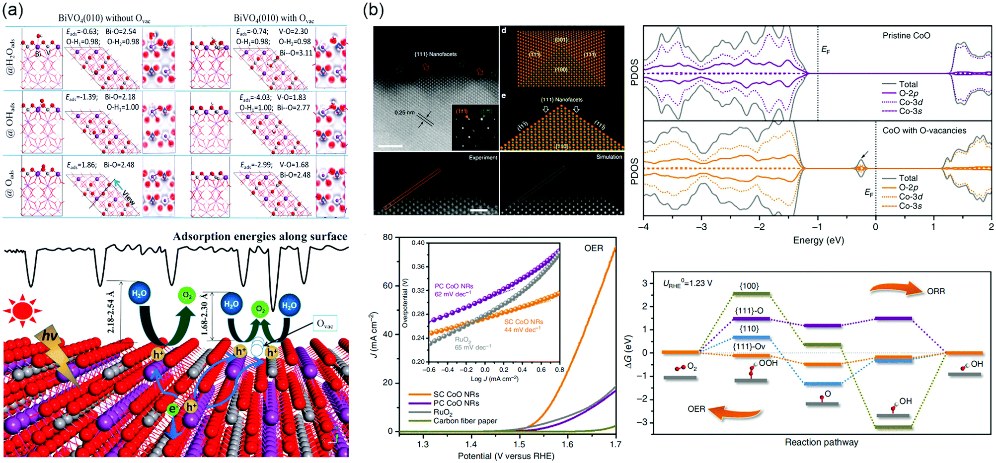 | ||
| Fig. 10 (a) Top: Adsorption structures, energies and electron density difference of H2Oads, OHads and Oads involved in a water splitting process on BiVO4 (010) facet with Ovac. Bottom: Schematic picture of the PEC water splitting process on BiVO4 (010) facet with or without Ovac. Adsorption energy along surface is illustrated. Reproduced with permission.256 Copyright 2017 American Chemical Society. (b) Upper left: High-resolution HAADF-STEM image taken from the outermost surface of a single SC CoO NR revealing the exposed {111} nanofacets, with inset showing the corresponding selected area electron diffraction pattern taken from [110] zone axis. Scale bar is 2 nm. Experimental and simulated HADDF-STEM images of the pyramidal structure, respectively. Scale bar is 1 nm. Atomic model of a nanopyramid enclosed with {100} and {111} facets, and the projection of this pyramidal structure along [110] zone axis. Bottom left: OER LSVs of SC, PC CoO NRs and commercial RuO2 catalysts directly deposited on CFP in O2-saturated1 M KOH solution at scan rate of 0.5 mV s−1 without iR correction, with the corresponding OER Tafel plots shown in inset. Upper right: The calculated ORR/OER free energy diagram at the equilibrium potential on different facets. Bottom right: The projected density of states (PDOS) on pristine CoO and CoO with O-vacancies. Reproduced with permission.264 Copyright 2016 Springer Nature. | ||
The oxygen reduction reaction (ORR) and OER are the essential processes for water splitting, fuel cell, and metal–air batteries. However, the ORR and OER process involve four electron transfer processes with sluggish reaction kinetics. Precious Pt and Ir based electrocatalysts are needed, limiting its large-scale utilization. Low-cost TMOs electrocatalysts such as Co3O4, NiO, LaNiO3, La1−xSrxCoO3−δ, etc., have been developed in the past few decades.257–260 The presence of defects significantly affects the band structure of catalysts and the local bond environment of defect sites, and hence manipulates the adsorption sites, energy, and configuration of the reactant or various intermediate species.261–263 Ling et al. synthesized CoO nanorods with oxygen-terminated {111} facets, where contain a large number of O-vacancies.264 It is worth mentioning that an additional state of hybridization of O 2p, Co-3d and Co 3s appears in the bandgap when introducing VO, which results in the lowest adsorption energies of intermediates on active sites, as shown in Fig. 10b. During the reaction process, owing to |ΔGOOH*| ≈ |ΔGO*| ≈ |ΔGOH*| ≈ 0, that the {111}-VO surface can adsorb and desorb easily. Based on the single-crystalline ultrathin Co3O4 model, it was able to further discuss the effect of defects on electrocatalytic performance by introducing vacancies into specific crystal facets.265 The Co3O4 {111} surface with rich VO exposed second-layered Co sites and then these Co atoms become the active sites under the influence of neighboring O atoms. This structure exhibits a low overpotential of 220 mV and improved electrical conductivity. In addition, superfluous VO will affect the stability of electrodes, filling heteroatoms in favor of compensating the coordination numbers and increasing the binding between intermediates and surface of electrocatalysts.266
Defects can also cause charge compensation and also play as scattering centers to affect the transport properties like mobility and conductivity, and even create lattice distortions and form strain. Cheng et al. prepared a rutile β-MnO2 with native VO, and the charge is compensated by the reduction of Mn4+ to Mn3+.267 It is remarkable that a new crystal structure appeared except a typical pyrolusite lattice, which can be explained by introduced VO. In this case, electrodes exhibit a more positive potential and a large current for ORR. The work of Zhao et al. emphasized that the Mn3+ active sites of ultrathin δ-MnO2 nanosheets contribute to half-metallicity and strong H2O adsorption.268 There are two valences, Co2+ and Co3+, in Co3O4. Some studies have demonstrated that Co3+ is the key active site of the ORR, and that relative ratio of Co2+/Co3+ can be tuned by controlling the concentration of VO.266,269 Besides, the methane catalytic combustion of Ca-doped LaFeO3 perovskites show a directly correlation to the amount of Fe4+, which results from the formation of VO.270
In addition, grain boundaries, steps, and edges also belong to defects. It is generally true that these defects are thermodynamically unstable, and have high energy and low coordination number, which leads to improved electrocatalytic performance. The broken symmetry near grain boundaries increases the binding energy of intermediate species.271,272 However, in some cases of photocatalysis, it is easy to be trapped and recombined when charge carriers transfer through the grain boundaries and then inhibit catalytic activity.273,274
3.9 Ionic doping
Ionotronics is an emerging technology that aims to induce a large change of transport properties through the movement of ionic doping by an external stimuli. By moving ions, such as H+, Li+, Na+ and Mg2+, into or out of TMOs under an electric field, reversible changes in the structure, electronic structure and physical properties of TMOs can be achieved. Ionic doping across solid–liquid interfaces can be realized using ionic liquid, aqueous solutions or water. In ionic liquid gating, due to a very strong electric field (≥10 MV cm−1) formed at the interface, hydrogen ions can be intercalated into TMOs from the ionic liquid, or oxygen ions can be moved out from TMOs, depending on the polarity of the electric field. As shown in Fig. 11a, using ionic liquids, controlling the insertion and extraction of hydrogen and oxygen ions independently of each other can direct reversible phase transformations among three different materials phases: HSrCoO2.5, brownmillerite SrCoO2.5 and perovskite SrCoO3.275 Consequently, Lu et al. observed a dramatic modulation of electronic, magnetic and optical properties by changing the valence state of Co and Co 3d and O 2p orbital hybridization. Moreover, the electric-field control of three different magnetic ground states was also reported (Fig. 11b).19 Very recently, the tuning of thermal conductivity was further demonstrated by triggering the “tri-state” phase transitions in SrCoO2.5 films (Fig. 11c).275 Similar reversible phase transformations mediated by hydrogen and oxygen ions was also observed in VO2, ZnO, WO3, SrRuO3, La1−xSrxMnO3, La0.7Sr0.3MnO3/SrIrO3 superlattice films, etc.18,164,276–281 Water was also used as a gating medium for achieving hydrogen doping.282 The ionization of water to form H+ and OH− occurs when a bias voltage over 1.23 V is applied between an electrode and TMOs in water. Thus, under a positive electric field, H+ can be intercalated into TMOs. It has been reported that a water-infiltrated nanoporous glass or a humid air gap can be used for controlling the channel conductance in SrTiO3 and VO2 field effect transistors, respectively.283,284 In addition, H+ doping through solid–gas interface was studied in SmNiO3 and VO2 films.20,276,285 Pt electrodes were used for achieving effective H+ doping, which changes electron doping and suppresses the electronic transport via electron–electron correlations.20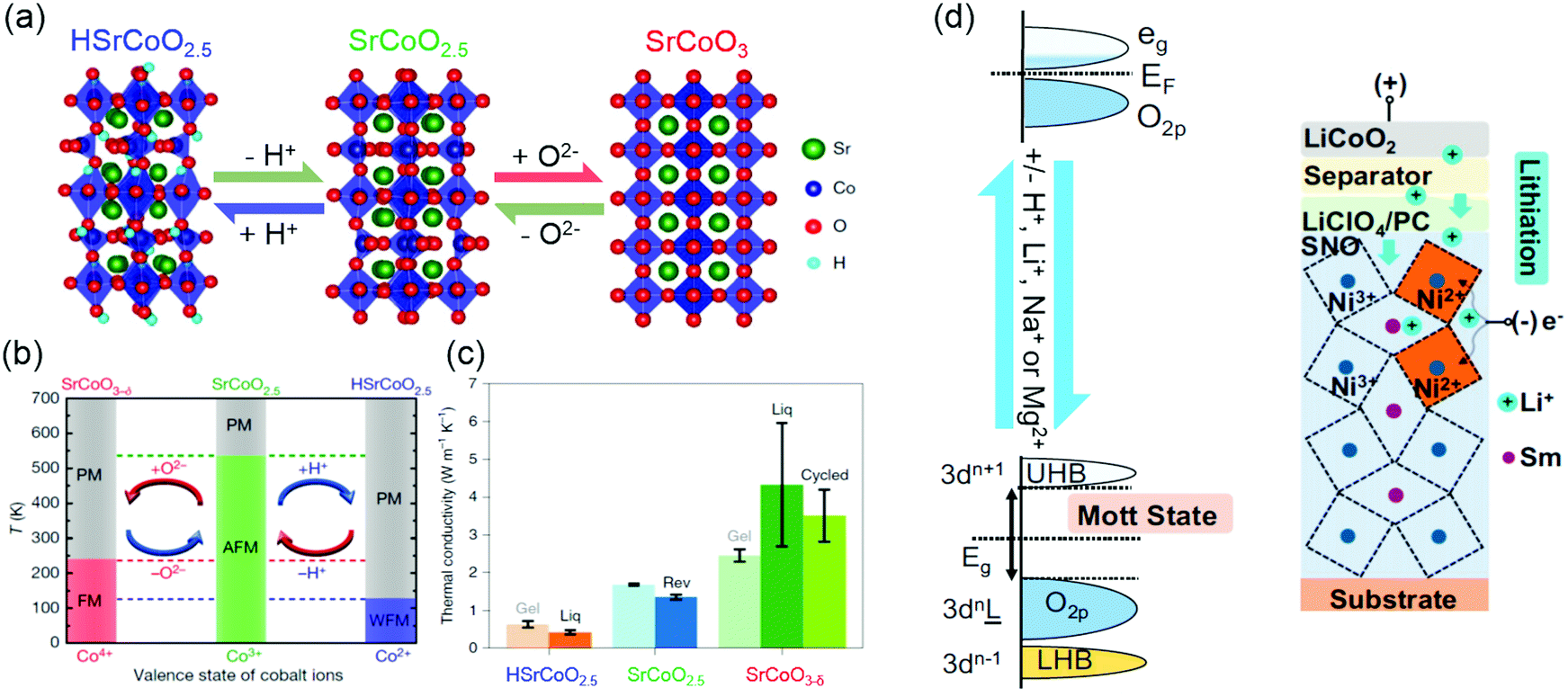 | ||
| Fig. 11 (a) Reversible phase transformation of SrCoO2.5 through the dual-ion (O2− and H+) switch. Reproduced with permission.275 Copyright 2020 Springer Nature. (b) Magnetoelectric effects in different temperature regions. Red and blue arrows represent negative and positive voltages, respectively. PM, paramagnetism; FM, ferromagnetism; AFM, antiferromagnetism; WFM, weak ferromagnetism. Reproduced with permission.19 Copyright 2017 Springer Nature. (c) Thermal conductivities of HSrCoO2.5, SrCoO2.5 and SrCoO3−δ films. Reproduced with permission.275 Copyright 2020 Springer Nature. (d) Left panel: Band diagram of SmNiO3 before (top) and after ionic doping (bottom). Eg is the band gap. Right panel: Electrochemical cell for lithiation of SmNiO3. Reproduced with permission.286 Copyright 2018 National Academy of Sciences. | ||
Ionic doping across solid–solid interfaces can be realized using solid state electrolytes. When a positive bias is applied across a proton-storing solid-state electrolyte, hydrogen ions can be injected into TMOs. The advantage of this doping method is that not only H+ but also Li+, Na+, and Mg2+ intercalation can take place in a controlled manner by gating through electrochemical cells. As shown in Fig. 11d, pristine room temperature SmNiO3 is a semiconductor with a narrow bandgap.20,286 After ionic doping, it becomes a strongly correlated insulator, with a bandgap on the order of 3 eV, where Ni3+ is reduced to Ni2+. Furthermore, electric-field-induced ion injection is non-volatile and reversible. After removal of an applied electric field, ionic dopants remain in TMOs, and the application of a reverse electric-field can be used to remove them. Therefore, these phenomena can be exploited for the use in non-volatile memory devices with cross-bar or related geometries.
The reversible manipulation of physical and chemical properties in TMOs using ionic doping can be used in a wide range of applications, such as electronics (e.g., sensors,287 non-volatile memory,288 smart windows, etc.),19,289 energy (e.g., catalysis for water splitting, fuel cell, etc.),290–292 and emerging research directions (e.g., biomimetric machine learning, synaptic transistor, etc.).179,293–296 More comprehensive discussions on these topics can be found in recent published reviews.21,282,297
3.10 Wide bandgap oxide semiconductors
Wide bandgap oxide semiconductors are widely utilized in the field of flat-panel displays (FPDs), sensing devices and power electronics due to their fascinating opto-electrical properties, compositional diversities, structural stability and adjustable bandgap values.43,298–301 Motivated by the great promises of oxide semiconductors and devices, great efforts have been made to modulate their performances from different angles including mobility, carrier type (electron or hole), crystallinity, transparency, etc. Defect engineering has been one of the core strategies in controlling oxide semiconductor properties.302–304 Here we will take some representative oxide semiconductors (ZnO, In2O3, IGZO) as examples, to discuss how the control of defects, such as VO, VC and interstitials, could help to shape materials and devices.ZnO is probably the most remarkable oxide semiconductor. With a direct bandgap of 3.4 eV, large exciton energy (60 meV), low cost and easiness of growing large single crystals, ZnO seems like a very attractive candidate for optoelectronics.305,306 Despite its intrinsic advantages, the lack of control over dopants and defects hindered its further application to practical devices, thus stimulated a boom over investigating the defect chemistry in ZnO.302,307–310 The as-grown ZnO crystals normally exhibit n-type conductivity, which was initially attributed to the native defects such as Zn interstitials, Zn vacancies or VO (Fig. 12a).302,305 However, VO has been proven to be deep donors311–313 and Zn vacancies form as compensating acceptors in n-type ZnO.314,315 Zn interstitials are proved to be shallow donors,315,316 yet they are unstable at room temperature due to their mobile nature.317,318 Group-III donors (B, Al, Ga, and In) and H impurities account for most of the n-type conductivity in ZnO samples. To reach an applicable doping level of n ∼ 1020 cm−3 as required by a transparent conductor, H is a shallow donor in ZnO and has been shown great improvement of carrier concentrations with the magnitude of 3 orders.319–322 Despite multiple experimental and theoretical investigations having been devoted to the microscopic structure of H in defects323–326 and its complex with Zn vacancies or other impurities,327–329 its interaction with the ZnO crystal lattice or components and the mechanism of modulating carrier transportation are still not very clear.
In2O3 is firstly known as the parent material of widely used transparent semiconducting oxide indium-tin-oxide (ITO).330–333 In the last decade, In2O3 itself has been rediscovered to be a wide-bandgap semiconductor with great potential and has received lots of attentions from the semiconductor physics community,299 due to its fascinating structural,334–337 mechanical338–340 and electronic properties.341–344 The explorations of the influence of defects on conductivity of In2O3 has a long history. Bierwagen et al. summarized the results of Hall mobility and Hall electron concentration in unintentionally doped, In2O3 thin films and bulk samples and observed a qualitatively similar trend, that simultaneously increased in electron mobility and decreased electron concentration, consistent with O2 annealing reduced donor concentration, as shown in Fig. 12b.299 Discrepancies remain regarding the nature of native defects. DFT calculations within LDA/GGA by Lany et al.313 and Limpijumnong et al.345 reached the conclusion that VO are deep donors, while Ágoston et al. calculated them to be shallow donors using the hybrid-functional method within DFT.346,347 Calculations by Tang et al. suggested that even though VO creates deep donor levels,348 In interstitials lead to shallow donors and their coupling with VO could give rise to even shallower donors. The native defects also have important influences on the doping modulation of In2O3. While dopant solubility is sufficient in In2O3, native defects normally act as compensating centers, i.e., donor-type defects VO and In interstitials tend to counteract p-type doping, while acceptor-type defects, i.e. In vacancies and O interstitials, counteract n-type doping.313,349 The control over the In2O3 native defects concentrations could be realized by simply adjusting the growth conditions. For example, VO could be controlled by varying the growth atmosphere or by adding an additional O2 annealing process.350,351
Amorphous indium gallium zinc oxide (a-IGZO) is one of the most successful commercialized oxide semiconductors in this century, widely used in thin-film transistors (TFTs) for high-resolution displays.298,352–355 Defects have a significant influence on a-IGZO materials and TFTs, i.e., while most defects are detrimental to device performance, some defects actually play a positive role in improving carrier density.304,356,357 VO, metal–metal bonds and H incorporation are the three main defect types present in channel region of a-IGZO TFTs.358 VO could participate in several different local coordination structures: (i) ‘Corner-share’ structure formed by VO coordinated with small numbers of cations, (ii) ‘Free space’ structure formed by VO adjacent to a large open space and (iii) ‘Edge/Face-sharing’ structure formed by VO surrounded by many cations, as shown in Fig. 12c.298 The ‘Corner-share’ and ‘Free space’ structures act as both deep and shallow traps, reducing the electron concentration.359 The deep traps mainly result in the increase of subthreshold swing and indirectly increase the device operating voltage, while shallow traps contribute to the hysteresis in device performance.360–362 The ‘Edge/Face-sharing’ structure act as shallow donors, which is the main source of carriers in a-IGZO and thus vital for device charge transport.298,352,363,364 Several methods have been proposed to control VO in a-IGZO, including modulating the growth atmosphere (oxygen partial pressure)365–367 and post deposition annealing.368,369 The metal–metal bonds are associated to VO, formed by the binding of uncoordinated metal ions caused by deficient oxygen to eliminate the dangling bonds.355 Additional sub-gap states are induced near CBM by metal–metal bonds and could significantly increase the off-state leakage current Ioff.356,370,371 Reduction of metal–metal bonds generally follows the path with the decrease of VO, yet they are harder to eliminate for the additional energy required to break the bonds.357 The incorporation of hydrogen could happen during annealing processes or by diffusion of other materials in TFT devices, i.e., gate dielectrics, passivation layers or buffer layers.372–374 The role of hydrogen in a-IGZO varies under different H concentrations. At lower concentrations lower than ∼2 × 1021 cm−3, hydrogen improves the device performance by passivating O-related defects either through bonding with weakly bound oxygen to form –OH or replacing the VO, thus reducing hysteresis and increasing carrier density.375–377 At higher concentrations above 2 × 1021 cm−3, additional hydrogen in a-IGZO might create a conductive channel near the dielectric interface that negatively shifts the turn-on voltage.375 Currently reported sub-gap defects and their influences on electronic structure of IGZO are summarized by Ide et al.304 as shown in Fig. 12d.
 | ||
| Fig. 12 (a) Structural diagram hydrogen defects in ZnO: Interstitial hydrogen donors (bottom) with antibonding (bottom left) and bond-centered (bottom right) configurations, and nitrogen–hydrogen complex (top). The dashed lines indicate broken Zn–O bonds. Reproduced with permission.302,328 Copyright 2009 American Institue of Phyiscs and Copyright 2007 American Physcial Society. (b) Hall mobility and Hall electron concentration in unintentionally doped (UID), In2O3 thin films and bulk samples. The decreasing electron concentration with simultaneous increase of mobility after annealing in oxygen-containing atmosphere is shown. Reproduced with permission.299 Copyright 2010 American Institue of Phyiscs. (c) Local coordination structures of some oxygen deficiencies in IGZO. The red spheres represent O ions, green spheres are Ga, grey spheres are Zn and pink spheres are In atoms. The red spheres indicated by the arrows are oxygen vacancy sites. ‘Corner-shared’, ‘Free-space’ and ‘Edge/Face-shared’ notation describes the structures around these oxygen vacancy sites. Reproduced with permission.298 Copyright 2010 Institue of Phyiscs. (d) Summary of known electronic structure of a-IGZO with subgap defects. Reproduced with permission.304 Copyright 2019 Wiley-VCH. | ||
4. Summary and perspective
Recent progress in the growth of high-quality TMOs epitaxial thin films, together with exploration of new systems and with the application of different stimuli to tune the structures and defects within them, has led to intriguing new physical phenomena. These phenomena are limited not only to the bulk of the films but also to the heterointerfaces between the different materials. There is huge potential range of new applications stemming from these, influencing every sector of industry from transport to energy to ICT to medicine. In this review, we highlight some of the many fascinating physical properties, ranging from insulating to semiconducting or metallic, exhibiting phenomena from ferroelectricity to transparency. We show how the underlying physics relies on the control of electronic structure, which is determined by the partially occupied TM d orbitals, the hybridization between TM d and oxygen 2p orbitals and the corresponding local atomic structures. We also highlight the importance of defects to electronic structure and chemical structure, and show the benefits of precise defect engineering for enhancing physical properties. However, we also show how that the strong influence of defects in TMOs is something of a double-edged sword: certain defects being engineerable and critical for realizing a desired functionality, while others are detrimental to expected properties and hard to control. In this latter regard, there are still many challenges to be solved, some key ones being summarized as following:(1) Unlike misfit dislocations, grain boundaries and domain walls, point defects formed by cation/oxygen vacancies and ionic doping (e.g., H+ and Li+) are ‘invisible’ because of their dilute concentrations. There is a huge demand for new techniques to be available that can allow us to observe cation/oxygen vacancies and ions at low concentrations and with large spatial accuracy. Therefore, new ways to directly, rapidly and simply characterise these point defects and to quantify their presence are of utmost importance for understanding defect-structure–property relations in memristors, in wide bandgap oxide semiconductors, at functional heterointerfaces, etc. With such techniques, a new world will be opened up for TMOs science and applications.
(2) Defects, strain and interfaces are usually entangled for tuning the functionalities in TMOs thin films. Hence, great care must be taken to separate these parameters from one another so as to enable their individual influence on the physical properties to be understood. On the other hand, similar to the implementation of semiconductors in devices, an important question is how to achieve precise control of defect (or impurity) concentrations and distributions in TMOs thin films. This will be important as there is an increasing drive towards miniaturization of electronic circuits and devices based on TMOs thin films. Furthermore, to achieve novel functionalities which utilise defects, an important question is how to dynamically characterise/control/tune the distribution of defects. To fulfill these purposes, many characterisation techniques (e.g., photoemission spectroscopy, transmission electron microscopy, scanning tunneling microscopy, scanning probe microscopy, X-ray techniques) usually working under vacuum conditions and/or room temperature, need to be customized to work in controlled environments and high temperatures, thereby enabling characterisation under in situ or even in operando conditions to monitor the dynamics of defects. Also, combining in situ and in operando techniques and first-principles calculations will allow for increasingly accurate characterisation of defects, strain and interfaces, and undoubtedly will improve the understanding of their individual roles in TMO devices during operation. Further developments in synthesis/growth of TMOs thin films will allow greater control of dynamic ionic defect profiles. In turn, it may be possible to exploit the different mobilities of cations and anions to engineer gradients in static and dynamic chemistry and carrier concentrations.
(3) Electrochemical reactions and ionic transport underpin the functionality of memristors, wide bandgap oxide semiconductors and electrochemical water splitting. When the bias voltage is applied for driving ionic motion, the irreversible/reversible redistribution of defects in TMOs thin films may occur. Consequently, the stability of defects in TMOs thin films is a key problem for the irreversible fatigue/degeneration of electronics and catalysts and needs to be addressed. One approach is to investigate static and dynamic ionic behaviour which will help us to understand the interaction between ionic motion and defects. Further progress, in both experimental and theoretical methodology, will be key for exploring and controlling the stability of defects in TMOs thin films for electronics and energy applications.
Conflicts of interest
The authors declare no competing financial interests.Acknowledgements
W.-W. L. and J. L. M.-D. acknowledge support from EPSRC Grant EP/L011700/1, EP/N004272/1, EP/T012218/1, and the Isaac Newton Trust (Minute 13.38(k)). J. L. M.-D. also acknowledges support from the Royal Academy of Engineering, Grant CiET1819_24, and the ERC POC grant, 779444, Portapower. K. H. L. Z. is grateful for funding support from the National Natural Science Foundation of China (Grant No. 21872116).References
- J. L. MacManus-Driscoll, M. P. Wells, C. Yun, J.-W. Lee, C.-B. Eom and D. G. Schlom, APL Mater., 2020, 8, 040904 CrossRef.
- S. A. Chambers, Surf. Sci. Rep., 2000, 39, 105–180 CrossRef CAS.
- Z. Huang, A. Ariando, X. Renshaw Wang, A. Rusydi, J. Chen, H. Yang and T. Venkatesan, Adv. Mater., 2018, 30, 1802439 CrossRef PubMed.
- S. Saremi, R. Gao, A. Dasgupta and L. W. Martin, Am. Ceram. Soc. Bull., 2018, 97, 16–23 CAS.
- J. F. Schooley, W. R. Hosler and M. L. Cohen, Phys. Rev. Lett., 1964, 12, 474–475 CrossRef CAS.
- J. F. Schooley, W. R. Hosler, E. Ambler, J. H. Becker, M. L. Cohen and C. S. Koonce, Phys. Rev. Lett., 1965, 14, 305–307 CrossRef CAS.
- C. S. Koonce, M. L. Cohen, J. F. Schooley, W. R. Hosler and E. R. Pfeiffer, Phys. Rev., 1967, 163, 380–390 CrossRef CAS.
- W. D. Rice, P. Ambwani, M. Bombeck, J. D. Thompson, G. Haugstad, C. Leighton and S. A. Crooker, Nat. Mater., 2014, 13, 481–487 CrossRef CAS PubMed.
- D. Lee, H. Lu, Y. Gu, S.-Y. Choi, S.-D. Li, S. Ryu, T. R. Paudel, K. Song, E. Mikheev, S. Lee, S. Stemmer, D. A. Tenne, S. H. Oh, E. Y. Tsymbal, X. Wu, L.-Q. Chen, A. Gruverman and C. B. Eom, Science, 2015, 349, 1314–1317 CrossRef CAS PubMed.
- K. Klyukin and V. Alexandrov, Phys. Rev. B, 2017, 95, 035301 CrossRef.
- I. Sugiyama, N. Shibata, Z. Wang, S. Kobayashi, T. Yamamoto and Y. Ikuhara, Nat. Nanotechnol., 2013, 8, 266–270 CrossRef CAS PubMed.
- R. Gross, L. Alff, B. Büchner, B. H. Freitag, C. Höfener, J. Klein, Y. Lu, W. Mader, J. B. Philipp, M. S. R. Rao, P. Reutler, S. Ritter, S. Thienhaus, S. Uhlenbruck and B. Wiedenhorst, J. Magn. Magn. Mater., 2000, 211, 150–159 CrossRef CAS.
- Z. Zhang, W. Sigle and M. Rühle, Phys. Rev. B: Condens. Matter Mater. Phys., 2002, 66, 094108 CrossRef.
- P. Gao, S. Yang, R. Ishikawa, N. Li, B. Feng, A. Kumamoto, N. Shibata, P. Yu and Y. Ikuhara, Phys. Rev. Lett., 2018, 120, 267601 CrossRef CAS.
- J. Seidel, L. W. Martin, Q. He, Q. Zhan, Y. H. Chu, A. Rother, M. E. Hawkridge, P. Maksymovych, P. Yu, M. Gajek, N. Balke, S. V. Kalinin, S. Gemming, F. Wang, G. Catalan, J. F. Scott, N. A. Spaldin, J. Orenstein and R. Ramesh, Nat. Mater., 2009, 8, 229–234 CrossRef CAS.
- M. L. Medarde, J. Phys.: Condens. Matter, 1997, 9, 1679–1707 CrossRef CAS.
- H. Y. Hwang, S. W. Cheong, P. G. Radaelli, M. Marezio and B. Batlogg, Phys. Rev. Lett., 1995, 75, 914–917 CrossRef CAS.
- H. Yuan, H. Shimotani, A. Tsukazaki, A. Ohtomo, M. Kawasaki and Y. Iwasa, J. Am. Chem. Soc., 2010, 132, 6672–6678 CrossRef CAS PubMed.
- N. Lu, P. Zhang, Q. Zhang, R. Qiao, Q. He, H.-B. Li, Y. Wang, J. Guo, D. Zhang, Z. Duan, Z. Li, M. Wang, S. Yang, M. Yan, E. Arenholz, S. Zhou, W. Yang, L. Gu, C.-W. Nan, J. Wu, Y. Tokura and P. Yu, Nature, 2017, 546, 124–128 CrossRef CAS PubMed.
- J. Shi, Y. Zhou and S. Ramanathan, Nat. Commun., 2014, 5, 4860 CrossRef CAS PubMed.
- H.-T. Zhang, Z. Zhang, H. Zhou, H. Tanaka, D. D. Fong and S. Ramanathan, Adv. Phys.: X, 2019, 4, 1523686 CAS.
- J. B. Goodenough, Rep. Prog. Phys., 2004, 67, 1915–1993 CrossRef CAS.
- H. L. Tuller and S. R. Bishop, Annu. Rev. Mater. Res., 2011, 41, 369–398 CrossRef CAS.
- S. V. Kalinin and N. A. Spaldin, Science, 2013, 341, 858–859 CrossRef CAS.
- A. Herklotz, D. Lee, E.-J. Guo, T. L. Meyer, J. R. Petrie and H. N. Lee, J. Phys.: Condens. Matter, 2017, 29, 493001 CrossRef PubMed.
- A. De Vita, M. J. Gillan, J. S. Lin, M. C. Payne, I. Štich and L. J. Clarke, Phys. Rev. B: Condens. Matter Mater. Phys., 1992, 46, 12964–12973 CrossRef CAS PubMed.
- A. Gibson, R. Haydock and J. P. LaFemina, Phys. Rev. B: Condens. Matter Mater. Phys., 1994, 50, 2582–2592 CrossRef CAS PubMed.
- M. V. Ganduglia-Pirovano, A. Hofmann and J. Sauer, Surf. Sci. Rep., 2007, 62, 219–270 CrossRef CAS.
- K. H. L. Zhang, G. Li, S. R. Spurgeon, L. Wang, P. Yan, Z. Wang, M. Gu, T. Varga, M. E. Bowden, Z. Zhu, C. Wang and Y. Du, ACS Appl. Mater. Interfaces, 2018, 10, 17480–17486 CrossRef CAS PubMed.
- J. Robertson, J. Appl. Phys., 2003, 93, 1054–1059 CrossRef CAS.
- F. El-Mellouhi, E. N. Brothers, M. J. Lucero and G. E. Scuseria, J. Phys.: Condens. Matter, 2013, 25, 135501 CrossRef.
- T. Shi, Y. Chen and X. Guo, Prog. Mater. Sci., 2016, 80, 77–132 CrossRef CAS.
- S. Lany, J. Osorio-Guillén and A. Zunger, Phys. Rev. B: Condens. Matter Mater. Phys., 2007, 75, 241203 CrossRef.
- W.-L. Jang, Y.-M. Lu, W.-S. Hwang, T.-L. Hsiung and H. P. Wang, Appl. Phys. Lett., 2009, 94, 062103 CrossRef.
- X. Huang, J. Zhang, M. Wu, S. Zhang, H. Xiao, W. Han, T.-L. Lee, A. Tadich, D.-C. Qi, L. Qiao, L. Chen and K. H. L. Zhang, Phys. Rev. B, 2019, 100, 115301 CrossRef CAS.
- H. Raebiger, S. Lany and A. Zunger, Phys. Rev. B: Condens. Matter Mater. Phys., 2007, 76, 045209 CrossRef.
- J. Y. Zhang, W. W. Li, R. L. Z. Hoye, J. L. MacManus-Driscoll, M. Budde, O. Bierwagen, L. Wang, Y. Du, M. J. Wahila, L. F. J. Piper, T. L. Lee, H. J. Edwards, V. R. Dhanak and K. H. L. Zhang, J. Mater. Chem. C, 2018, 6, 2275–2282 RSC.
- S.-H. Yoon and H. Kim, J. Appl. Phys., 2002, 92, 1039–1047 CrossRef CAS.
- P. Blennow, A. Hagen, K. K. Hansen, L. R. Wallenberg and M. Mogensen, Solid State Ionics, 2008, 179, 2047–2058 CrossRef CAS.
- T. Saitoh, A. E. Bocquet, T. Mizokawa, H. Namatame, A. Fujimori, M. Abbate, Y. Takeda and M. Takano, Phys. Rev. B: Condens. Matter Mater. Phys., 1995, 51, 13942–13951 CrossRef CAS PubMed.
- K. Horiba, A. Chikamatsu, H. Kumigashira, M. Oshima, N. Nakagawa, M. Lippmaa, K. Ono, M. Kawasaki and H. Koinuma, Phys. Rev. B: Condens. Matter Mater. Phys., 2005, 71, 155420 CrossRef.
- K. H. L. Zhang, Y. Du, A. Papadogianni, O. Bierwagen, S. Sallis, L. F. Piper, M. E. Bowden, V. Shutthanandan, P. V. Sushko and S. A. Chambers, Adv. Mater., 2015, 27, 5191–5195 CrossRef CAS PubMed.
- K. H. L. Zhang, K. Xi, M. G. Blamire and R. G. Egdell, J. Phys.: Condens. Matter, 2016, 28, 383002 CrossRef PubMed.
- M. Dawber, K. M. Rabe and J. F. Scott, Rev. Mod. Phys., 2005, 77, 1083–1130 CrossRef CAS.
- N. Setter, D. Damjanovic, L. Eng, G. Fox, S. Gevorgian, S. Hong, A. Kingon, H. Kohlstedt, N. Y. Park, G. B. Stephenson, I. Stolitchnov, A. K. Taganstev, D. V. Taylor, T. Yamada and S. Streiffer, J. Appl. Phys., 2006, 100, 051606 CrossRef.
- G. H. Haertling, J. Am. Ceram. Soc., 1999, 82, 797–818 CrossRef CAS.
- J. F. Scott, Science, 2007, 315, 954–959 CrossRef CAS PubMed.
- A. Kursumovic, W. W. Li, S. Cho, P. J. Curran, D. H. L. Tjhe and J. L. MacManus-Driscoll, Nano Energy, 2020, 71, 104536 CrossRef CAS.
- R. Mishra, Y.-M. Kim, J. Salafranca, S. K. Kim, S. H. Chang, A. Bhattacharya, D. D. Fong, S. J. Pennycook, S. T. Pantelides and A. Y. Borisevich, Nano Lett., 2014, 14, 2694–2701 CrossRef CAS PubMed.
- O. Chmaissem, B. Dabrowski, S. Kolesnik, J. Mais, D. E. Brown, R. Kruk, P. Prior, B. Pyles and J. D. Jorgensen, Phys. Rev. B: Condens. Matter Mater. Phys., 2001, 64, 134412 CrossRef.
- C. Becher, L. Maurel, U. Aschauer, M. Lilienblum, C. Magén, D. Meier, E. Langenberg, M. Trassin, J. Blasco, I. P. Krug, P. A. Algarabel, N. A. Spaldin, J. A. Pardo and M. Fiebig, Nat. Nanotechnol., 2015, 10, 661–665 CrossRef CAS PubMed.
- H. Kim, J. Y. Zhang, S. Raghavan and S. Stemmer, Phys. Rev. X, 2016, 6, 041063 Search PubMed.
- D. Lee, B. C. Jeon, S. H. Baek, S. M. Yang, Y. J. Shin, T. H. Kim, Y. S. Kim, J.-G. Yoon, C. B. Eom and T. W. Noh, Adv. Mater., 2012, 24, 6490–6495 CrossRef CAS PubMed.
- A. R. Damodaran, E. Breckenfeld, Z. Chen, S. Lee and L. W. Martin, Adv. Mater., 2014, 26, 6341–6347 CrossRef CAS PubMed.
- X. Ren, Nat. Mater., 2004, 3, 91–94 CrossRef CAS PubMed.
- S. Saremi, J. Kim, A. Ghosh, D. Meyers and L. W. Martin, Phys. Rev. Lett., 2019, 123, 207602 CrossRef CAS PubMed.
- H. Lu, D. Lee, K. Klyukin, L. Tao, B. Wang, H. Lee, J. Lee, T. R. Paudel, L.-Q. Chen, E. Y. Tsymbal, V. Alexandrov, C.-B. Eom and A. Gruverman, Nano Lett., 2018, 18, 491–497 CrossRef CAS PubMed.
- R. Gao, S. E. Reyes-Lillo, R. Xu, A. Dasgupta, Y. Dong, L. R. Dedon, J. Kim, S. Saremi, Z. Chen, C. R. Serrao, H. Zhou, J. B. Neaton and L. W. Martin, Chem. Mater., 2017, 29, 6544–6551 CrossRef CAS.
- M.-W. Chu, I. Szafraniak, R. Scholz, C. Harnagea, D. Hesse, M. Alexe and U. Gösele, Nat. Mater., 2004, 3, 87–90 CrossRef CAS PubMed.
- P. Gao, C. T. Nelson, J. R. Jokisaari, S.-H. Baek, C. W. Bark, Y. Zhang, E. Wang, D. G. Schlom, C.-B. Eom and X. Pan, Nat. Commun., 2011, 2, 591 CrossRef PubMed.
- X. Y. Zhang, R. X. Xu, X. Y. Gao, M. Li, X. N. Shi, Y. D. Ji, F. J. Qian, J. Y. Fan, H. Y. Wang, W.-W. Li and H. Yang, Appl. Surf. Sci., 2020, 516, 146093 CrossRef CAS.
- X. Zhang, R. Xu, X. Gao, Y. Ji, F. Qian, J. Fan, H. Wang, W.-W. Li and H. Yang, J. Mater. Chem. C, 2020, 8, 8091 RSC.
- V. Nagarajan, C. L. Jia, H. Kohlstedt, R. Waser, I. B. Misirlioglu, S. P. Alpay and R. Ramesh, Appl. Phys. Lett., 2005, 86, 192910 CrossRef.
- A. L. Roytburd, Phase Transitions, 1993, 45, 1–34 CrossRef CAS.
- J. Seidel, P. Maksymovych, Y. Batra, A. Katan, S. Y. Yang, Q. He, A. P. Baddorf, S. V. Kalinin, C. H. Yang, J. C. Yang, Y. H. Chu, E. K. H. Salje, H. Wormeester, M. Salmeron and R. Ramesh, Phys. Rev. Lett., 2010, 105, 197603 CrossRef CAS PubMed.
- J. Guyonnet, I. Gaponenko, S. Gariglio and P. Paruch, Adv. Mater., 2011, 23, 5377–5382 CrossRef CAS PubMed.
- S. Farokhipoor and B. Noheda, Phys. Rev. Lett., 2011, 107, 127601 CrossRef CAS PubMed.
- S. Y. Yang, J. Seidel, S. J. Byrnes, P. Shafer, C. H. Yang, M. D. Rossell, P. Yu, Y. H. Chu, J. F. Scott, J. W. Ager, L. W. Martin and R. Ramesh, Nat. Nanotechnol., 2010, 5, 143–147 CrossRef CAS PubMed.
- A. Gupta, G. Q. Gong, G. Xiao, P. R. Duncombe, P. Lecoeur, P. Trouilloud, Y. Y. Wang, V. P. Dravid and J. Z. Sun, Phys. Rev. B: Condens. Matter Mater. Phys., 1996, 54, R15629–R15632 CrossRef CAS PubMed.
- N. D. Mathur, G. Burnell, S. P. Isaac, T. J. Jackson, B. S. Teo, J. L. MacManus-Driscoll, L. F. Cohen, J. E. Evetts and M. G. Blamire, Nature, 1997, 387, 266–268 CrossRef CAS.
- U. Aschauer, R. Pfenninger, S. M. Selbach, T. Grande and N. A. Spaldin, Phys. Rev. B: Condens. Matter Mater. Phys., 2013, 88, 054111 CrossRef.
- M. Li, C. Tang, T. R. Paudel, D. Song, W. Lü, K. Han, Z. Huang, S. Zeng, X. Renshaw Wang, P. Yang, A. Ariando, J. Chen, T. Venkatesan, E. Y. Tsymbal, C. Li and S. J. Pennycook, Adv. Mater., 2019, 31, 1901386 CrossRef PubMed.
- S. Cheng, M. Li, S. Deng, S. Bao, P. Tang, W. Duan, J. Ma, C. Nan and J. Zhu, Adv. Funct. Mater., 2016, 26, 3589–3598 CrossRef CAS.
- C. G. Shull, W. A. Strauser and E. O. Wollan, Phys. Rev., 1951, 83, 333–345 CrossRef CAS.
- K. H. L. Zhang, R. Wu, F. Tang, W. Li, F. E. Oropeza, L. Qiao, V. K. Lazarov, Y. Du, D. J. Payne, J. L. Macmanus-Driscoll and M. G. Blamire, ACS Appl. Mater. Interfaces, 2017, 9, 26549–26555 CrossRef CAS PubMed.
- H. Jeen, W. S. Choi, J. W. Freeland, H. Ohta, C. U. Jung and H. N. Lee, Adv. Mater., 2013, 25, 3651–3656 CrossRef CAS PubMed.
- K. H. L. Zhang, P. V. Sushko, R. Colby, Y. Du, M. E. Bowden and S. A. Chambers, Nat. Commun., 2014, 5, 4669 CrossRef CAS PubMed.
- L. Cao, O. Petracic, P. Zakalek, A. Weber, U. Rücker, J. Schubert, A. Koutsioubas, S. Mattauch and T. Brückel, Adv. Mater., 2019, 31, 1806183 CrossRef PubMed.
- H. Jeen, W. S. Choi, M. D. Biegalski, C. M. Folkman, I. C. Tung, D. D. Fong, J. W. Freeland, D. Shin, H. Ohta, M. F. Chisholm and H. N. Lee, Nat. Mater., 2013, 12, 1057–1063 CrossRef CAS PubMed.
- J. H. Jang, Y.-M. Kim, Q. He, R. Mishra, L. Qiao, M. D. Biegalski, A. R. Lupini, S. T. Pantelides, S. J. Pennycook, S. V. Kalinin and A. Y. Borisevich, ACS Nano, 2017, 11, 6942–6949 CrossRef CAS PubMed.
- A. Khare, D. Shin, T. S. Yoo, M. Kim, T. D. Kang, J. Lee, S. Roh, I.-H. Jung, J. Hwang, S. W. Kim, T. W. Noh, H. Ohta and W. S. Choi, Adv. Mater., 2017, 29, 1606566 CrossRef PubMed.
- A. Muñoz, C. De La Calle, J. A. Alonso, P. M. Botta, V. Pardo, D. Baldomir and J. Rivas, Phys. Rev. B: Condens. Matter Mater. Phys., 2008, 78, 054404 CrossRef.
- J. Gazquez, S. Bose, M. Sharma, M. A. Torija, S. J. Pennycook, C. Leighton and M. Varela, APL Mater., 2013, 1, 012105 CrossRef.
- Y.-M. Kim, J. He, M. D. Biegalski, H. Ambaye, V. Lauter, H. M. Christen, S. T. Pantelides, S. J. Pennycook, S. V. Kalinin and A. Y. Borisevich, Nat. Mater., 2012, 11, 888–894 CrossRef CAS PubMed.
- M. Merz, P. Nagel, C. Pinta, A. Samartsev, H. v. Löhneysen, M. Wissinger, S. Uebe, A. Assmann, D. Fuchs and S. Schuppler, Phys. Rev. B: Condens. Matter Mater. Phys., 2010, 82, 174416 CrossRef.
- W. S. Choi, J.-H. Kwon, H. Jeen, J. E. Hamann-Borrero, A. Radi, S. Macke, R. Sutarto, F. He, G. A. Sawatzky, V. Hinkov, M. Kim and H. N. Lee, Nano Lett., 2012, 12, 4966–4970 CrossRef CAS PubMed.
- N. Biškup, J. Salafranca, V. Mehta, M. P. Oxley, Y. Suzuki, S. J. Pennycook, S. T. Pantelides and M. Varela, Phys. Rev. Lett., 2014, 112, 087202 CrossRef.
- V. V. Mehta, N. Biskup, C. Jenkins, E. Arenholz, M. Varela and Y. Suzuki, Phys. Rev. B: Condens. Matter Mater. Phys., 2015, 91, 144418 CrossRef.
- M. B. Salamon and M. Jaime, Rev. Mod. Phys., 2001, 73, 583–628 CrossRef CAS.
- J. M. Rondinelli and N. A. Spaldin, Adv. Mater., 2011, 23, 3363–3381 CrossRef CAS PubMed.
- Y. Tokura and N. Nagaosa, Science, 2000, 288, 462–468 CrossRef CAS PubMed.
- D. Pesquera, G. Herranz, A. Barla, E. Pellegrin, F. Bondino, E. Magnano, F. Sánchez and J. Fontcuberta, Nat. Commun., 2012, 3, 1189 CrossRef CAS PubMed.
- A. Sadoc, B. Mercey, C. Simon, D. Grebille, W. Prellier and M.-B. Lepetit, Phys. Rev. Lett., 2010, 104, 046804 CrossRef PubMed.
- L. Qiao, J. H. Jang, D. J. Singh, Z. Gai, H. Xiao, A. Mehta, R. K. Vasudevan, A. Tselev, Z. Feng, H. Zhou, S. Li, W. Prellier, X. Zu, Z. Liu, A. Borisevich, A. P. Baddorf and M. D. Biegalski, Nano Lett., 2015, 15, 4677–4684 CrossRef CAS PubMed.
- W.-W. Li, B. Zhu, Q. He, A. Y. Borisevich, C. Yun, R. Wu, P. Lu, Z. Qi, Q. Wang, A. Chen, H. Wang, S. A. Cavill, K. H. L. Zhang and J. L. MacManus-Driscoll, Adv. Sci., 2020, 7, 1901606 CrossRef CAS PubMed.
- J. M. Rondinelli, S. J. May and J. W. Freeland, MRS Bull., 2012, 37, 261–270 CrossRef CAS.
- E. J. Moon, R. Colby, Q. Wang, E. Karapetrova, C. M. Schlepütz, M. R. Fitzsimmons and S. J. May, Nat. Commun., 2014, 5, 5710 CrossRef CAS PubMed.
- J. M. Rondinelli and S. Coh, Phys. Rev. Lett., 2011, 106, 235502 CrossRef PubMed.
- X. Zhai, L. Cheng, Y. Liu, C. M. Schlepütz, S. Dong, H. Li, X. Zhang, S. Chu, L. Zheng, J. Zhang, A. Zhao, H. Hong, A. Bhattacharya, J. N. Eckstein and C. Zeng, Nat. Commun., 2014, 5, 4283 CrossRef CAS PubMed.
- A. J. Grutter, A. Vailionis, J. A. Borchers, B. J. Kirby, C. L. Flint, C. He, E. Arenholz and Y. Suzuki, Nano Lett., 2016, 16, 5647–5651 CrossRef CAS PubMed.
- Z. Liao, M. Huijben, Z. Zhong, N. Gauquelin, S. Macke, R. J. Green, S. Van Aert, J. Verbeeck, G. Van Tendeloo, K. Held, G. A. Sawatzky, G. Koster and G. Rijnders, Nat. Mater., 2016, 15, 425–431 CrossRef CAS PubMed.
- D. Kan, R. Aso, R. Sato, M. Haruta, H. Kurata and Y. Shimakawa, Nat. Mater., 2016, 15, 432–437 CrossRef CAS PubMed.
- D. G. Schlom, L.-Q. Chen, C.-B. Eom, K. M. Rabe, S. K. Streiffer and J.-M. Triscone, Annu. Rev. Mater. Res., 2007, 37, 589–626 CrossRef CAS.
- N. A. Spaldin and M. Fiebig, Science, 2005, 309, 391–392 CrossRef CAS PubMed.
- W. Eerenstein, N. D. Mathur and J. F. Scott, Nature, 2006, 442, 759–765 CrossRef CAS PubMed.
- R. Ramesh and N. A. Spaldin, Nat. Mater., 2007, 6, 21–29 CrossRef CAS PubMed.
- K. F. Wang, J. M. Liu and Z. F. Ren, Adv. Phys., 2009, 58, 321–448 CrossRef CAS.
- N. A. Spaldin, S.-W. Cheong and R. Ramesh, Phys. Today, 2010, 63, 38 CrossRef.
- N. A. Hill, J. Phys. Chem. B, 2000, 104, 6694–6709 CrossRef CAS.
- G. A. Smolenskiĭ and I. E. Chupis, Phys.-Usp., 1982, 25, 475–493 CrossRef.
- J. Wang, J. B. Neaton, H. Zheng, V. Nagarajan, S. B. Ogale, B. Liu, D. Viehland, V. Vaithyanathan, D. G. Schlom, U. V. Waghmare, N. A. Spaldin, K. M. Rabe, M. Wuttig and R. Ramesh, Science, 2003, 299, 1719–1722 CrossRef CAS PubMed.
- J. Přívratská and V. Janovec, Ferroelectrics, 1997, 204, 321–331 CrossRef.
- Q. He, C. H. Yeh, J. C. Yang, G. Singh-Bhalla, C. W. Liang, P. W. Chiu, G. Catalan, L. W. Martin, Y. H. Chu, J. F. Scott and R. Ramesh, Phys. Rev. Lett., 2012, 108, 067203 CrossRef CAS PubMed.
- A. Lubk, M. D. Rossell, J. Seidel, Y. H. Chu, R. Ramesh, M. J. Hÿtch and E. Snoeck, Nano Lett., 2013, 13, 1410–1415 CrossRef CAS PubMed.
- P. Agrawal, M. Campanini, A. Rappe, S. Liu, V. Grillo, C. Hébert, R. Erni, D. Passerone and M. D. Rossell, Phys. Rev. Mater., 2019, 3, 034410 CrossRef CAS.
- K. T. Kang, C. J. Roh, J. Lim, T. Min, J. H. Lee, K. Lee, T. Y. Lee, S. Kang, D. Seol, J. Kim, H. Ohta, A. Khare, S. Park, Y. Kim, S. C. Chae, Y. S. Oh, J. Lee, J. Yu, J. S. Lee and W. S. Choi, Adv. Mater., 2019, 31, 1808104 CrossRef PubMed.
- W.-W. Li, R. Zhao, L. Wang, R. Tang, Y. Zhu, J. H. Lee, H. Cao, T. Cai, H. Guo, C. Wang, L. Ling, L. Pi, K. Jin, Y. Zhang, H. Wang, Y. Wang, S. Ju and H. Yang, Sci. Rep., 2013, 3, 2618 CrossRef PubMed.
- W.-W. Li, Q. He, L. Wang, H. Zeng, J. Bowlan, L. Ling, D. A. Yarotski, W. Zhang, R. Zhao, J. Dai, J. Gu, S. Shen, H. Guo, L. Pi, H. Wang, Y. Wang, I. A. Velasco-Davalos, Y. Wu, Z. Hu, B. Chen, R.-W. Li, Y. Sun, K. Jin, Y. Zhang, H.-T. Chen, S. Ju, A. Ruediger, D. Shi, A. Y. Borisevich and H. Yang, Phys. Rev. B, 2017, 96, 115105 CrossRef.
- H. Das, A. L. Wysocki, Y. Geng, W. Wu and C. J. Fennie, Nat. Commun., 2014, 5, 2998 CrossRef PubMed.
- J. A. Mundy, C. M. Brooks, M. E. Holtz, J. A. Moyer, H. Das, A. F. Rébola, J. T. Heron, J. D. Clarkson, S. M. Disseler, Z. Liu, A. Farhan, R. Held, R. Hovden, E. Padgett, Q. Mao, H. Paik, R. Misra, L. F. Kourkoutis, E. Arenholz, A. Scholl, J. A. Borchers, W. D. Ratcliff, R. Ramesh, C. J. Fennie, P. Schiffer, D. A. Muller and D. G. Schlom, Nature, 2016, 537, 523–527 CrossRef CAS PubMed.
- M. J. Pitcher, P. Mandal, M. S. Dyer, J. Alaria, P. Borisov, H. Niu, J. B. Claridge and M. J. Rosseinsky, Science, 2015, 347, 420–424 CrossRef CAS PubMed.
- A. Chen, H. Zhou, Z. Bi, Y. Zhu, Z. Luo, A. Bayraktaroglu, J. Phillips, E.-M. Choi, J. L. MacManus-Driscoll, S. J. Pennycook, J. Narayan, Q. Jia, X. Zhang and H. Wang, Adv. Mater., 2013, 25, 1028–1032 CrossRef CAS PubMed.
- E.-M. Choi, T. Fix, A. Kursumovic, C. J. Kinane, D. Arena, S.-L. Sahonta, Z. Bi, J. Xiong, L. Yan, J.-S. Lee, H. Wang, S. Langridge, Y.-M. Kim, A. Y. Borisevich, I. MacLaren, Q. M. Ramasse, M. G. Blamire, Q. Jia and J. L. MacManus-Driscoll, Adv. Funct. Mater., 2014, 24, 7478–7487 CrossRef CAS PubMed.
- C. Homes, T. Vogt, S. Shapiro, S. Wakimoto and A. Ramirez, Science, 2001, 293, 673–676 CrossRef CAS PubMed.
- S. Krohns, P. Lunkenheimer, S. Meissner, A. Reller, B. Gleich, A. Rathgeber, T. Gaugler, H. U. Buhl, D. C. Sinclair and A. Loidl, Nat. Mater., 2011, 10, 899–901 CrossRef CAS PubMed.
- C.-H. Lee, N. D. Orloff, T. Birol, Y. Zhu, V. Goian, E. Rocas, R. Haislmaier, E. Vlahos, J. A. Mundy, L. F. Kourkoutis, Y. Nie, M. D. Biegalski, J. Zhang, M. Bernhagen, N. A. Benedek, Y. Kim, J. D. Brock, R. Uecker, X. X. Xi, V. Gopalan, D. Nuzhnyy, S. Kamba, D. A. Muller, I. Takeuchi, J. C. Booth, C. J. Fennie and D. G. Schlom, Nature, 2013, 502, 532–536 CrossRef CAS PubMed.
- O. Lee, S. A. Harrington, A. Kursumovic, E. Defay, H. Wang, Z. Bi, C.-F. Tsai, L. Yan, Q. Jia and J. L. MacManus-Driscoll, Nano Lett., 2012, 12, 4311–4317 CrossRef CAS PubMed.
- A. L. Sangle, O. J. Lee, A. Kursumovic, W. Zhang, A. Chen, H. Wang and J. L. MacManus-Driscoll, Nanoscale, 2018, 10, 3460–3468 RSC.
- H. Yang, H. Wang, J. Yoon, Y. Wang, M. Jain, D. M. Feldmann, P. C. Dowden, J. L. MacManus-Driscoll and Q. Jia, Adv. Mater., 2009, 21, 3794–3798 CrossRef CAS.
- R. Zhao, W.-W. Li, A. Chen, W. Zhang, J. Yang, Y. Liang, R. Tang, H. Wang and H. Yang, Appl. Phys. Lett., 2014, 105, 072907 CrossRef.
- S. A. Harrington, J. Zhai, S. Denev, V. Gopalan, H. Wang, Z. Bi, S. A. T. Redfern, S.-H. Baek, C. W. Bark, C.-B. Eom, Q. Jia, M. E. Vickers and J. L. MacManus-Driscoll, Nat. Nanotechnol., 2011, 6, 491–495 CrossRef CAS PubMed.
- W.-W. Li, R. Zhao, R. Tang, A. Chen, W. Zhang, X. Lu, H. Wang and H. Yang, ACS Appl. Mater. Interfaces, 2014, 6, 5356–5361 CrossRef CAS PubMed.
- W.-W. Li, W. Zhang, L. Wang, J. Gu, A. Chen, R. Zhao, Y. Liang, H. Guo, R. Tang, C. Wang, K. Jin, H. Wang and H. Yang, Sci. Rep., 2015, 5, 11335 CrossRef PubMed.
- W.-W. Li, J. Gu, Q. He, K. H. L. Zhang, C. Wang, K. Jin, Y. Wang, M. Acosta, H. Wang, A. Y. Borisevich, J. L. MacManus-Driscoll and H. Yang, Appl. Phys. Lett., 2018, 112, 182906 CrossRef.
- A. Ohtomo and H. Y. Hwang, Nature, 2004, 427, 423–426 CrossRef CAS PubMed.
- S. Thiel, G. Hammerl, A. Schmehl, C. W. Schneider and J. Mannhart, Science, 2006, 313, 1942–1945 CrossRef CAS PubMed.
- Y. Chen, N. Pryds, J. E. Kleibeuker, G. Koster, J. Sun, E. Stamate, B. Shen, G. Rijnders and S. Linderoth, Nano Lett., 2011, 11, 3774–3778 CrossRef CAS PubMed.
- S. A. Chambers, L. Qiao, T. C. Droubay, T. C. Kaspar, B. W. Arey and P. Sushko, Phys. Rev. Lett., 2011, 107, 206802 CrossRef CAS PubMed.
- N. Reyren, S. Thiel, A. Caviglia, L. F. Kourkoutis, G. Hammerl, C. Richter, C. W. Schneider, T. Kopp, A.-S. Rüetschi and D. Jaccard, Science, 2007, 317, 1196–1199 CrossRef CAS PubMed.
- J. Mannhart and D. Schlom, Science, 2010, 327, 1607–1611 CrossRef CAS PubMed.
- C. Cen, S. Thiel, J. Mannhart and J. Levy, Science, 2009, 323, 1026–1030 CrossRef CAS PubMed.
- A. D. Caviglia, S. Gariglio, C. Cancellieri, B. Sacépé, A. Fête, N. Reyren, M. Gabay, A. F. Morpurgo and J. M. Triscone, Phys. Rev. Lett., 2010, 105, 236802 CrossRef CAS PubMed.
- L. Qiao, T. C. Droubay, T. C. Kaspar, P. V. Sushko and S. A. Chambers, Surf. Sci., 2011, 605, 1381–1387 CrossRef CAS.
- L. Qiao, T. C. Droubay, T. Varga, M. E. Bowden, V. Shutthanandan, Z. Zhu, T. C. Kaspar and S. A. Chambers, Phys. Rev. B: Condens. Matter Mater. Phys., 2011, 83, 085408 CrossRef.
- G. Herranz, M. Basletić, M. Bibes, C. Carrétéro, E. Tafra, E. Jacquet, K. Bouzehouane, C. Deranlot, A. Hamzić, J. M. Broto, A. Barthélémy and A. Fert, Phys. Rev. Lett., 2007, 98, 216803 CrossRef CAS PubMed.
- W. Siemons, G. Koster, H. Yamamoto, W. A. Harrison, G. Lucovsky, T. H. Geballe, D. H. A. Blank and M. R. Beasley, Phys. Rev. Lett., 2007, 98, 196802 CrossRef PubMed.
- C. Cancellieri, N. Reyren, S. Gariglio, A. D. Caviglia, A. Fête and J. M. Triscone, Europhys. Lett., 2010, 91, 17004 CrossRef.
- A. Brinkman, M. Huijben, M. van Zalk, J. Huijben, U. Zeitler, J. C. Maan, W. G. van der Wiel, G. Rijnders, D. H. A. Blank and H. Hilgenkamp, Nat. Mater., 2007, 6, 493–496 CrossRef CAS PubMed.
- N. Nakagawa, H. Y. Hwang and D. A. Muller, Nat. Mater., 2006, 5, 204–209 CrossRef CAS.
- H. Lee, N. Campbell, J. Lee, T. J. Asel, T. R. Paudel, H. Zhou, J. W. Lee, B. Noesges, J. Seo, B. Park, L. J. Brillson, S. H. Oh, E. Y. Tsymbal, M. S. Rzchowski and C. B. Eom, Nat. Mater., 2018, 17, 231–236 CrossRef CAS PubMed.
- P. Zubko, S. Gariglio, M. Gabay, P. Ghosez and J.-M. Triscone, Annu. Rev. Condens. Matter Phys., 2011, 2, 141–165 CrossRef CAS.
- J. Mannhart, D. H. A. Blank, H. Y. Hwang, A. J. Millis and J. M. Triscone, MRS Bull., 2008, 33, 1027–1034 CrossRef CAS.
- S. A. Chambers, M. H. Engelhard, V. Shutthanandan, Z. Zhu, T. C. Droubay, L. Qiao, P. V. Sushko, T. Feng, H. D. Lee, T. Gustafsson, E. Garfunkel, A. B. Shah, J. M. Zuo and Q. M. Ramasse, Surf. Sci. Rep., 2010, 65, 317–352 CrossRef CAS.
- M. Imada, A. Fujimori and Y. Tokura, Rev. Mod. Phys., 1998, 70, 1039–1263 CrossRef CAS.
- M. Uehara, S. Mori, C. H. Chen and S. W. Cheong, Nature, 1999, 399, 560–563 CrossRef CAS.
- L. Zhang, C. Israel, A. Biswas, R. Greene and A. De Lozanne, Science, 2002, 298, 805–807 CrossRef CAS PubMed.
- E. Dagotto, Science, 2005, 309, 257–262 CrossRef CAS PubMed.
- K. H. L. Zhang, Y. Du, P. V. Sushko, M. E. Bowden, V. Shutthanandan, S. Sallis, L. F. J. Piper and S. A. Chambers, Phys. Rev. B: Condens. Matter Mater. Phys., 2015, 91, 155129 CrossRef.
- Z. Yang, C. Ko and S. Ramanathan, Annu. Rev. Mater. Res., 2011, 41, 337–367 CrossRef CAS.
- D. M. Newns, J. A. Misewich, C. C. Tsuei, A. Gupta, B. A. Scott and A. Schrott, Appl. Phys. Lett., 1998, 73, 780–782 CrossRef CAS.
- F. J. Morin, Phys. Rev. Lett., 1959, 3, 34–36 CrossRef CAS.
- Y. Muraoka and Z. Hiroi, Appl. Phys. Lett., 2002, 80, 583–585 CrossRef CAS.
- L. L. Fan, S. Chen, Z. L. Luo, Q. H. Liu, Y. F. Wu, L. Song, D. X. Ji, P. Wang, W. S. Chu, C. Gao, C. W. Zou and Z. Y. Wu, Nano Lett., 2014, 14, 4036–4043 CrossRef CAS PubMed.
- H. Ji, J. Wei and D. Natelson, Nano Lett., 2012, 12, 2988–2992 CrossRef CAS PubMed.
- Z. Zhang, F. Zuo, C. Wan, A. Dutta, J. Kim, J. Rensberg, R. Nawrodt, H. H. Park, T. J. Larrabee, X. Guan, Y. Zhou, S. M. Prokes, C. Ronning, V. M. Shalaev, A. Boltasseva, M. A. Kats and S. Ramanathan, Phys. Rev. Appl., 2017, 7, 034008 CrossRef.
- Y. Ji, Q. Yang, X. Zhang, R. Xu, W. Liang, R. Zhao, W. Li, X. Ou and H. Yang, Appl. Phys. Lett., 2019, 115, 201603 CrossRef.
- J. Jeong, N. Aetukuri, T. Graf, T. D. Schladt, M. G. Samant and S. S. Parkin, Science, 2013, 339, 1402–1405 CrossRef CAS PubMed.
- Y. Zhou and S. Ramanathan, J. Appl. Phys., 2012, 111, 084508 CrossRef.
- D. Lee, B. Chung, Y. Shi, G.-Y. Kim, N. Campbell, F. Xue, K. Song, S.-Y. Choi, J. Podkaminer and T. Kim, Science, 2018, 362, 1037–1040 CrossRef CAS PubMed.
- E. Enriquez, A. Chen, Z. Harrell, X. Lü, P. Dowden, N. Koskelo, M. Janoschek, C. Chen and Q. Jia, Appl. Phys. Lett., 2016, 109, 141906 CrossRef.
- S. Catalano, M. Gibert, J. Fowlie, J. Íñiguez, J. M. Triscone and J. Kreisel, Rep. Prog. Phys., 2018, 81, 046501 CrossRef CAS PubMed.
- R. K. Patel, D. Meyers, X. Liu, P. Mandal, M. Kareev, P. Shafer, J.-W. Kim, P. J. Ryan, S. Middey and J. Chakhalian, APL Mater., 2020, 8, 041113 CrossRef.
- J. B. Torrance, P. Lacorre, A. I. Nazzal, E. J. Ansaldo and C. Niedermayer, Phys. Rev. B: Condens. Matter Mater. Phys., 1992, 45, 8209–8212 CrossRef CAS PubMed.
- T. Mizokawa, D. I. Khomskii and G. A. Sawatzky, Phys. Rev. B: Condens. Matter Mater. Phys., 2000, 61, 11263–11266 CrossRef CAS.
- H. Raebiger, S. Lany and A. Zunger, Nature, 2008, 453, 763–766 CrossRef CAS PubMed.
- H. Park, A. J. Millis and C. A. Marianetti, Phys. Rev. Lett., 2012, 109, 156402 CrossRef PubMed.
- V. Bisogni, S. Catalano, R. J. Green, M. Gibert, R. Scherwitzl, Y. Huang, V. N. Strocov, P. Zubko, S. Balandeh, J.-M. Triscone, G. Sawatzky and T. Schmitt, Nat. Commun., 2016, 7, 13017 CrossRef CAS PubMed.
- I. V. Nikulin, M. A. Novojilov, A. R. Kaul, S. N. Mudretsova and S. V. Kondrashov, Mater. Res. Bull., 2004, 39, 775–791 CrossRef CAS.
- J. Shi, S. D. Ha, Y. Zhou, F. Schoofs and S. Ramanathan, Nat. Commun., 2013, 4, 2676 CrossRef PubMed.
- M. Kawai, S. Inoue, M. Mizumaki, N. Kawamura, N. Ichikawa and Y. Shimakawa, Appl. Phys. Lett., 2009, 94, 082102 CrossRef.
- M. Kotiuga, Z. Zhang, J. Li, F. Rodolakis, H. Zhou, R. Sutarto, F. He, Q. Wang, Y. Sun and Y. Wang, Proc. Natl. Acad. Sci. U. S. A., 2019, 116, 21992–21997 CrossRef CAS PubMed.
- A. Mercy, J. Bieder, J. Íñiguez and P. Ghosez, Nat. Commun., 2017, 8, 1677 CrossRef PubMed.
- Z. Liao, N. Gauquelin, R. J. Green, K. Müller-Caspary, I. Lobato, L. Li, S. Van Aert, J. Verbeeck, M. Huijben and M. N. Grisolia, Proc. Natl. Acad. Sci. U. S. A., 2018, 115, 9515–9520 CrossRef CAS PubMed.
- I. Valov, R. Waser, J. R. Jameson and M. N. Kozicki, Nanotechnology, 2011, 22, 289502 CrossRef.
- R. Waser and M. Aono, Nat. Mater., 2007, 6, 833–840 CrossRef CAS PubMed.
- Y. Bernard, V. T. Renard, P. Gonon and V. Jousseaume, Microelectron. Eng., 2011, 88, 814–816 CrossRef CAS.
- Y. Yang, P. Gao, S. Gaba, T. Chang, X. Pan and W. Lu, Nat. Commun., 2012, 3, 732 CrossRef PubMed.
- J. J. Yang, J. Borghetti, D. Murphy, D. R. Stewart and R. S. Williams, Adv. Mater., 2009, 21, 3754–3758 CrossRef CAS.
- R. Waser, R. Dittmann, G. Staikov and K. Szot, Adv. Mater., 2009, 21, 2632–2663 CrossRef CAS.
- D.-H. Kwon, K. M. Kim, J. H. Jang, J. M. Jeon, M. H. Lee, G. H. Kim, X.-S. Li, G.-S. Park, B. Lee, S. Han, M. Kim and C. S. Hwang, Nat. Nanotechnol., 2010, 5, 148–153 CrossRef CAS PubMed.
- M.-J. Lee, C. B. Lee, D. Lee, S. R. Lee, M. Chang, J. H. Hur, Y.-B. Kim, C.-J. Kim, D. H. Seo, S. Seo, U. I. Chung, I.-K. Yoo and K. Kim, Nat. Mater., 2011, 10, 625–630 CrossRef CAS PubMed.
- J.-Y. Chen, C.-L. Hsin, C.-W. Huang, C.-H. Chiu, Y.-T. Huang, S.-J. Lin, W.-W. Wu and L.-J. Chen, Nano Lett., 2013, 13, 3671–3677 CrossRef CAS PubMed.
- D.-j. Seong, M. Jo, D. Lee and H. Hwang, Electrochem. Solid-State Lett., 2007, 10, H168 CrossRef CAS.
- K. M. Kim, B. J. Choi, M. H. Lee, G. H. Kim, S. J. Song, J. Y. Seok, J. H. Yoon, S. Han and C. S. Hwang, Nanotechnology, 2011, 22, 254010 CrossRef PubMed.
- T. Fujii, M. Kawasaki, A. Sawa, Y. Kawazoe, H. Akoh and Y. Tokura, Phys. Rev. B: Condens. Matter Mater. Phys., 2007, 75, 165101 CrossRef.
- S. Lee, A. Sangle, P. Lu, A. Chen, W. Zhang, J. S. Lee, H. Wang, Q. Jia and J. L. MacManus-Driscoll, Adv. Mater., 2014, 26, 6284–6289 CrossRef CAS PubMed.
- S. Cho, C. Yun, S. Tappertzhofen, A. Kursumovic, S. Lee, P. Lu, Q. Jia, M. Fan, J. Jian, H. Wang, S. Hofmann and J. L. MacManus-Driscoll, Nat. Commun., 2016, 7, 12373 CrossRef CAS PubMed.
- G. Di Martino, S. Tappertzhofen, S. Hofmann and J. Baumberg, Small, 2016, 12, 1334–1341 CrossRef CAS PubMed.
- J. S. Lee, S. Lee and T. W. Noh, Appl. Phys. Rev., 2015, 2, 031303 Search PubMed.
- J. Zhu, T. Zhang, Y. Yang and R. Huang, Appl. Phys. Rev., 2020, 7, 011312 Search PubMed.
- Y. Zhang, Z. Wang, J. Zhu, Y. Yang, M. Rao, W. Song, Y. Zhuo, X. Zhang, M. Cui, L. Shen, R. Huang and J. J. Yang, Appl. Phys. Rev., 2020, 7, 011308 Search PubMed.
- M. Zhao, B. Gao, J. Tang, H. Qian and H. Wu, Appl. Phys. Rev., 2020, 7, 011301 Search PubMed.
- Z. Wang, H. Wu, G. W. Burr, C. S. Hwang, K. L. Wang, Q. Xia and J. J. Yang, Nat. Rev. Mater., 2020, 5, 173–195 CrossRef CAS.
- L. Malavasi, C. A. Fisher and M. S. Islam, Chem. Soc. Rev., 2010, 39, 4370–4387 RSC.
- N. Mahato, A. Banerjee, A. Gupta, S. Omar and K. Balani, Prog. Mater. Sci., 2015, 72, 141–337 CrossRef CAS.
- A. Chroneos, B. Yildiz, A. Tarancón, D. Parfitt and J. A. Kilner, Energy Environ. Sci., 2011, 4, 2774–2789 RSC.
- J. Garcia-Barriocanal, A. Rivera-Calzada, M. Varela, Z. Sefrioui, E. Iborra, C. Leon, S. J. Pennycook and J. Santamaria, Science, 2008, 321, 676–680 CrossRef CAS PubMed.
- T. J. Pennycook, M. J. Beck, K. Varga, M. Varela, S. J. Pennycook and S. T. Pantelides, Phys. Rev. Lett., 2010, 104, 115901 CrossRef PubMed.
- N. Schichtel, C. Korte, D. Hesse and J. Janek, Phys. Chem. Chem. Phys., 2009, 11, 3043–3048 RSC.
- M. Sillassen, P. Eklund, N. Pryds, E. Johnson, U. Helmersson and J. Bøttiger, Adv. Funct. Mater., 2010, 20, 2071–2076 CrossRef CAS.
- X. Aparicio-Anglès and N. H. De Leeuw, J. Am. Ceram. Soc., 2017, 100, 3329–3339 CrossRef.
- C. Korte, A. Peters, J. Janek, D. Hesse and N. Zakharov, Phys. Chem. Chem. Phys., 2008, 10, 4623–4635 RSC.
- A. Peters, C. Korte, D. Hesse, N. Zakharov and J. Janek, Solid State Ionics, 2007, 178, 67–76 CrossRef CAS.
- I. Kosacki, C. M. Rouleau, P. F. Becher, J. Bentley and D. H. Lowndes, Solid State Ionics, 2005, 176, 1319–1326 CrossRef CAS.
- S. Azad, O. A. Marina, C. M. Wang, L. Saraf, V. Shutthanandan, D. E. McCready, A. El-Azab, J. E. Jaffe, M. H. Engelhard and C. H. Peden, Appl. Phys. Lett., 2005, 86, 131906 CrossRef.
- S. Lee and J. L. MacManus-Driscoll, APL Mater., 2017, 5, 042304 CrossRef.
- A. Chen, Q. Su, H. Han, E. Enriquez and Q. Jia, Adv. Mater., 2019, 31, 1803241 CrossRef PubMed.
- S. Lee, W. Zhang, F. Khatkhatay, H. Wang, Q. Jia and J. L. MacManus-Driscoll, Nano Lett., 2015, 15, 7362–7369 CrossRef PubMed.
- S. M. Yang, S. Lee, J. Jian, W. Zhang, P. Lu, Q. Jia, H. Wang, T. Won Noh, S. V. Kalinin and J. L. MacManus-Driscoll, Nat. Commun., 2015, 6, 8588 CrossRef CAS PubMed.
- R. Gao, A. C. P. Jain, S. Pandya, Y. Dong, Y. Yuan, H. Zhou, L. R. Dedon, V. Thoréton, S. Saremi, R. Xu, A. Luo, T. Chen, V. Gopalan, E. Ertekin, J. Kilner, T. Ishihara, N. H. Perry, D. R. Trinkle and L. W. Martin, Adv. Mater., 2020, 32, 1905178 CrossRef CAS PubMed.
- S. Chu, Y. Cui and N. Liu, Nat. Mater., 2016, 16, 16–22 CrossRef PubMed.
- K. Sivula and R. van de Krol, Nat. Rev. Mater., 2016, 1, 15010 CrossRef CAS.
- J. Jian, G. Jiang, R. van de Krol, B. Wei and H. Wang, Nano Energy, 2018, 51, 457–480 CrossRef CAS.
- W.-W. Li, K. Jiang, Z. Li, S. Gong, R. L. Z. Hoye, Z. Hu, Y. Song, C. Tian, J. Kim, K. H. L. Zhang, S. Cho and J. L. MacManus-Driscoll, Adv. Energy Mater., 2018, 8, 1801972 CrossRef.
- C. Li, Z. Luo, T. Wang and J. Gong, Adv. Mater., 2018, 30, e1707502 CrossRef PubMed.
- S. Kment, F. Riboni, S. Pausova, L. Wang, L. Wang, H. Han, Z. Hubicka, J. Krysa, P. Schmuki and R. Zboril, Chem. Soc. Rev., 2017, 46, 3716–3769 RSC.
- G. Wang, H. Wang, Y. Ling, Y. Tang, X. Yang, R. C. Fitzmorris, C. Wang, J. Z. Zhang and Y. Li, Nano Lett., 2011, 11, 3026–3033 CrossRef CAS PubMed.
- S. Wang, P. Chen, J. H. Yun, Y. Hu and L. Wang, Angew. Chem., Int. Ed., 2017, 56, 8500–8504 CrossRef CAS PubMed.
- W.-J. Yin, H. Tang, S.-H. Wei, M. M. Al-Jassim, J. Turner and Y. Yan, Phys. Rev. B: Condens. Matter Mater. Phys., 2010, 82, 045106 CrossRef.
- C. W. Lai and S. Sreekantan, Int. J. Hydrogen Energy, 2013, 38, 2156–2166 CrossRef CAS.
- D. A. Wheeler, G. Wang, Y. Ling, Y. Li and J. Z. Zhang, Energy Environ. Sci., 2012, 5, 6682–6702 RSC.
- J. H. Kennedy, J. Karl and W. Frese, J. Electrochem. Soc., 1978, 125, 709–714 CrossRef CAS.
- W.-J. Yin, S.-H. Wei, M. M. Al-Jassim, J. Turner and Y. Yan, Phys. Rev. B: Condens. Matter Mater. Phys., 2011, 83, 155102 CrossRef.
- Y. Lin, Y. Xu, M. T. Mayer, Z. I. Simpson, G. McMahon, S. Zhou and D. Wang, J. Am. Chem. Soc., 2012, 134, 5508–5511 CrossRef CAS PubMed.
- X. Qi, G. She, M. Wang, L. Mu and W. Shi, Chem. Commun., 2013, 49, 5742–5744 RSC.
- S. Shen, C. X. Kronawitter, D. A. Wheeler, P. Guo, S. A. Lindley, J. Jiang, J. Z. Zhang, L. Guo and S. S. Mao, J. Mater. Chem. A, 2013, 1, 14498–14506 RSC.
- M. Li, Y. Yang, Y. Ling, W. Qiu, F. Wang, T. Liu, Y. Song, X. Liu, P. Fang, Y. Tong and Y. Li, Nano Lett., 2017, 17, 2490–2495 CrossRef CAS PubMed.
- M. A. Lukowski and S. Jin, J. Phys. Chem. C, 2011, 115, 12388–12395 CrossRef CAS.
- C. M. Tian, W.-W. Li, Y. M. Lin, Z. Z. Yang, L. Wang, Y. G. Du, H. Y. Xiao, L. Qiao, J. Y. Zhang, L. Chen, D.-C. Qi, J. L. Macmanus-Driscoll and K. H. L. Zhang, J. Phys. Chem. C, 2020, 124, 12548–12558 CrossRef CAS.
- Z. Fu, T. Jiang, Z. Liu, D. Wang, L. Wang and T. Xie, Electrochim. Acta, 2014, 129, 358–363 CrossRef CAS.
- N. T. Hahn and C. B. Mullins, Chem. Mater., 2010, 22, 6474–6482 CrossRef CAS.
- H. Liao, Y. Fan, Y. Lin, K. Wang, R. Li, X. Chen, K. H. Zhang and Y. Yang, 2020, arXiv preprint, arXiv:2002.02389.
- W. L. Yongcai Qiu, W. Chen, W. Chen, G. Zhou, P.-C. Hsu, R. Zhang, Z. Liang, S. Fan, Y. Zhang and Y. Cui, Sci. Adv., 2016, 2, e1501764 CrossRef PubMed.
- J. B. Min Zhou, Y. Xu, J. Zhang, J. Xie, M. Guan, C. Wang, L. Wen, Y. Lei and Y. Xie, ACS Nano, 2014, 8, 7088–7098 CrossRef PubMed.
- S. P. Berglund, A. J. E. Rettie, S. Hoang and C. B. Mullins, Phys. Chem. Chem. Phys., 2012, 14, 7065–7075 RSC.
- F. F. Abdi, N. Firet and R. van de Krol, ChemCatChem, 2013, 5, 490–496 CrossRef CAS.
- B. J. Morgan and G. W. Watson, Phys. Rev. B: Condens. Matter Mater. Phys., 2009, 80, 233102 CrossRef.
- A. Janotti, J. B. Varley, P. Rinke, N. Umezawa, G. Kresse and C. G. Van de Walle, Phys. Rev. B: Condens. Matter Mater. Phys., 2010, 81, 085212 CrossRef.
- H. Cui, W. Zhao, C. Yang, H. Yin, T. Lin, Y. Shan, Y. Xie, H. Gu and F. Huang, J. Mater. Chem. A, 2014, 2, 8612–8616 RSC.
- Z. Wang, C. Yang, T. Lin, H. Yin, P. Chen, D. Wan, F. Xu, F. Huang, J. Lin, X. Xie and M. Jiang, Energy Environ. Sci., 2013, 6, 3007–3014 RSC.
- C. M. Yim, C. L. Pang and G. Thornton, Phys. Rev. Lett., 2010, 104, 036806 CrossRef CAS PubMed.
- P. T. S. Stefan Wendt, E. Lira, G. K. H. Madsen, Z. Li, J. Ø. Hansen, J. Matthiesen, A. Blekinge-Rasmussen, E. Lægsgaard, B. Hammer and F. Besenbacher, Science, 2008, 320, 1755–1759 CrossRef PubMed.
- J. Gan, X. Lu, J. Wu, S. Xie, T. Zhai, M. Yu, Z. Zhang, Y. Mao, S. C. Wang, Y. Shen and Y. Tong, Sci. Rep., 2013, 3, 1021 CrossRef PubMed.
- H. L. Tan, A. Suyanto, A. T. D. Denko, W. H. Saputera, R. Amal, F. E. Osterloh and Y. H. Ng, Part. Part. Syst. Charact., 2017, 34, 1600290 CrossRef.
- J.-M. Wu, Y. Chen, L. Pan, P. Wang, Y. Cui, D. Kong, L. Wang, X. Zhang and J.-J. Zou, Appl. Catal., B, 2018, 221, 187–195 CrossRef CAS.
- J. Hu, X. Zhao, W. Chen, H. Su and Z. Chen, J. Phys. Chem. C, 2017, 121, 18702–18709 CrossRef CAS.
- A. Bergmann, E. Martinez-Moreno, D. Teschner, P. Chernev, M. Gliech, J. F. de Araujo, T. Reier, H. Dau and P. Strasser, Nat. Commun., 2015, 6, 8625 CrossRef CAS PubMed.
- J. T. Mefford, X. Rong, A. M. Abakumov, W. G. Hardin, S. Dai, A. M. Kolpak, K. P. Johnston and K. J. Stevenson, Nat. Commun., 2016, 7, 11053 CrossRef CAS PubMed.
- X. Rong, J. Parolin and A. M. Kolpak, ACS Catal., 2016, 6, 1153–1158 CrossRef CAS.
- T. Zhang, M.-Y. Wu, D.-Y. Yan, J. Mao, H. Liu, W.-B. Hu, X.-W. Du, T. Ling and S.-Z. Qiao, Nano Energy, 2018, 43, 103–109 CrossRef CAS.
- M. Cui, X. Ding, X. Huang, Z. Shen, T.-L. Lee, F. E. Oropeza, J. P. Hofmann, E. J. M. Hensen and K. H. L. Zhang, Chem. Mater., 2019, 31, 7618–7625 CrossRef CAS.
- G. Fu, X. Wen, S. Xi, Z. Chen, W.-W. Li, J.-Y. Zhang, A. Tadich, R. Wu, D.-C. Qi, Y. Du, J. Cheng and K. H. L. Zhang, Chem. Mater., 2019, 31, 419–428 CrossRef CAS.
- Z. Shen, Y. Zhuang, W.-W. Li, X. Huang, F. E. Oropeza, E. J. M. Hensen, J. P. Hofmann, M. Cui, A. Tadich, D. Qi, J. Cheng, J. Li and K. H. L. Zhang, J. Mater. Chem. A, 2020, 8, 4407–4415 RSC.
- T. Ling, D. Y. Yan, Y. Jiao, H. Wang, Y. Zheng, X. Zheng, J. Mao, X. W. Du, Z. Hu, M. Jaroniec and S. Z. Qiao, Nat. Commun., 2016, 7, 12876 CrossRef CAS PubMed.
- Z. Cai, Y. Bi, E. Hu, W. Liu, N. Dwarica, Y. Tian, X. Li, Y. Kuang, Y. Li, X.-Q. Yang, H. Wang and X. Sun, Adv. Energy Mater., 2018, 8, 1701694 CrossRef.
- Z. Xiao, Y. Wang, Y.-C. Huang, Z. Wei, C.-L. Dong, J. Ma, S. Shen, Y. Li and S. Wang, Energy Environ. Sci., 2017, 10, 2563–2569 RSC.
- F. Cheng, T. Zhang, Y. Zhang, J. Du, X. Han and J. Chen, Angew. Chem., Int. Ed., 2013, 52, 2474–2477 CrossRef CAS PubMed.
- Y. Zhao, C. Chang, F. Teng, Y. Zhao, G. Chen, R. Shi, G. I. N. Waterhouse, W. Huang and T. Zhang, Adv. Energy Mater., 2017, 7, 1700005 CrossRef.
- A. Restovic, E. Ríos, S. Barbato, J. Ortiz and J. L. Gautier, J. Electroanal. Chem., 2002, 522, 141–151 CrossRef CAS.
- G. Pecchi, M. G. Jiliberto, A. Buljan and E. J. Delgado, Solid State Ionics, 2011, 187, 27–32 CrossRef CAS.
- K.-S. Kim, W. J. Kim, H.-K. Lim, E. K. Lee and H. Kim, ACS Catal., 2016, 6, 4443–4448 CrossRef CAS.
- Y. Heo, S. Choi, J. Bak, H.-S. Kim, H. B. Bae and S.-Y. Chung, Adv. Energy Mater., 2018, 8, 1802481 CrossRef.
- S. Biswas, J. Husek, S. Londo and L. R. Baker, J. Phys. Chem. Lett., 2018, 9, 5047–5054 CrossRef CAS PubMed.
- M. Zhou, X. W. Lou and Y. Xie, Nano Today, 2013, 8, 598–618 CrossRef CAS.
- Q. Lu, S. Huberman, H. Zhang, Q. Song, J. Wang, G. Vardar, A. Hunt, I. Waluyo, G. Chen and B. Yildiz, Nat. Mater., 2020, 19, 655–662 CrossRef CAS PubMed.
- J. Wei, H. Ji, W. Guo, A. H. Nevidomskyy and D. Natelson, Nat. Nanotechnol., 2012, 7, 357–362 CrossRef CAS.
- M. Wang, S. Shen, J. Ni, N. Lu, Z. Li, H. B. Li, S. Yang, T. Chen, J. Guo, Y. Wang, H. Xiang and P. Yu, Adv. Mater., 2017, 29, 1703628 CrossRef PubMed.
- S. Chen, H. Zhou, X. Ye, Z. Chen, J. Zhao, S. Das, C. Klewe, L. Zhang, E. Lupi, P. Shafer, E. Arenholz, D. Jin, H. Huang, Y. Lu, X. Li, M. Wu, S. Ke, H. Xu, X. Zeng, C. Huang, L. W. Martin and L. Chen, Adv. Funct. Mater., 2019, 29, 1907072 CrossRef CAS.
- D. Yi, Y. Wang, O. M. J. van ’t Erve, L. Xu, H. Yuan, M. J. Veit, P. P. Balakrishnan, Y. Choi, A. T. N’Diaye, P. Shafer, E. Arenholz, A. Grutter, H. Xu, P. Yu, B. T. Jonker and Y. Suzuki, Nat. Commun., 2020, 11, 902 CrossRef CAS PubMed.
- Z. Li, S. Shen, Z. Tian, K. Hwangbo, M. Wang, Y. Wang, F. M. Bartram, L. He, Y. Lyu, Y. Dong, G. Wan, H. Li, N. Lu, J. Zang, H. Zhou, E. Arenholz, Q. He, L. Yang, W. Luo and P. Yu, Nat. Commun., 2020, 11, 184 CrossRef CAS PubMed.
- A. Molinari, P. M. Leufke, C. Reitz, S. Dasgupta, R. Witte, R. Kruk and H. Hahn, Nat. Commun., 2017, 8, 15339 CrossRef PubMed.
- T. Kanki and H. Tanaka, APL Mater., 2017, 5, 042303 CrossRef.
- T. Sasaki, H. Ueda, T. Kanki and H. Tanaka, Sci. Rep., 2015, 5, 17080 CrossRef CAS PubMed.
- H. Ohta, Y. Sato, T. Kato, S. Kim, K. Nomura, Y. Ikuhara and H. Hosono, Nat. Commun., 2010, 1, 118 CrossRef PubMed.
- H. Yoon, M. Choi, T. W. Lim, H. Kwon, K. Ihm, J. K. Kim, S. Y. Choi and J. Son, Nat. Mater., 2016, 15, 1113–1119 CrossRef CAS PubMed.
- Y. Sun, M. Kotiuga, D. Lim, B. Narayanan, M. Cherukara, Z. Zhang, Y. Dong, R. Kou, C. J. Sun, Q. Lu, I. Waluyo, A. Hunt, H. Tanaka, A. N. Hattori, S. Gamage, Y. Abate, V. G. Pol, H. Zhou, S. Sankaranarayanan, B. Yildiz, K. M. Rabe and S. Ramanathan, Proc. Natl. Acad. Sci. U. S. A., 2018, 115, 9672–9677 CrossRef CAS PubMed.
- Z. Zhang, D. Schwanz, B. Narayanan, M. Kotiuga, J. A. Dura, M. Cherukara, H. Zhou, J. W. Freeland, J. Li, R. Sutarto, F. He, C. Wu, J. Zhu, Y. Sun, K. Ramadoss, S. S. Nonnenmann, N. Yu, R. Comin, K. M. Rabe, S. Sankaranarayanan and S. Ramanathan, Nature, 2018, 553, 68–72 CrossRef CAS PubMed.
- U. Bauer, L. Yao, A. J. Tan, P. Agrawal, S. Emori, H. L. Tuller, S. van Dijken and G. S. Beach, Nat. Mater., 2015, 14, 174–181 CrossRef CAS PubMed.
- D. R. Rosseinsky and R. J. Mortimer, Adv. Mater., 2001, 13, 783–793 CrossRef CAS.
- Y. Zhou, X. Guan, H. Zhou, K. Ramadoss, S. Adam, H. Liu, S. Lee, J. Shi, M. Tsuchiya, D. D. Fong and S. Ramanathan, Nature, 2016, 534, 231–234 CrossRef CAS PubMed.
- Y. Koyama, T. E. Chin, U. Rhyner, R. K. Holman, S. R. Hall and Y. M. Chiang, Adv. Funct. Mater., 2006, 16, 492–498 CrossRef CAS.
- J. M. McFarland, A. G. Bondy, B. G. Cumming and D. A. Butts, Nat. Commun., 2014, 5, 4605 CrossRef CAS PubMed.
- C. Ge, C. X. Liu, Q. L. Zhou, Q. H. Zhang, J. Y. Du, J. K. Li, C. Wang, L. Gu, G. Z. Yang and K. J. Jin, Adv. Mater., 2019, 31, e1900379 CrossRef PubMed.
- H. Y. Huang, C. Ge, Q. H. Zhang, C. X. Liu, J. Y. Du, J. K. Li, C. Wang, L. Gu, G. Z. Yang and K. J. Jin, Adv. Funct. Mater., 2019, 29, 1902702 CrossRef.
- C. Ge, G. Li, Q.-l. Zhou, J.-y. Du, E.-j. Guo, M. He, C. Wang, G.-z. Yang and K.-j. Jin, Nano Energy, 2020, 67, 104268 CrossRef CAS.
- F. Zuo, P. Panda, M. Kotiuga, J. Li, M. Kang, C. Mazzoli, H. Zhou, A. Barbour, S. Wilkins, B. Narayanan, M. Cherukara, Z. Zhang, S. Sankaranarayanan, R. Comin, K. M. Rabe, K. Roy and S. Ramanathan, Nat. Commun., 2017, 8, 240 CrossRef PubMed.
- H.-T. Zhang, P. Panda, J. Lin, Y. Kalcheim, K. Wang, J. W. Freeland, D. D. Fong, S. Priya, I. K. Schuller, S. K. R. S. Sankaranarayanan, K. Roy and S. Ramanathan, Appl. Phys. Rev., 2020, 7, 011309 Search PubMed.
- T. Kamiya, K. Nomura and H. Hosono, Sci. Technol. Adv. Mater., 2010, 11, 044305 CrossRef PubMed.
- O. Bierwagen and J. S. Speck, Appl. Phys. Lett., 2010, 97, 072103 CrossRef.
- Z. Wang, P. K. Nayak, J. A. Caraveo-Frescas and H. N. Alshareef, Adv. Mater., 2016, 28, 3831–3892 CrossRef CAS PubMed.
- J. Zhang, J. Shi, D.-C. Qi, L. Chen and K. H. L. Zhang, APL Mater., 2020, 8, 020906 CrossRef.
- M. D. McCluskey and S. J. Jokela, J. Appl. Phys., 2009, 106, 071101 CrossRef.
- J. P. Allen, D. O. Scanlon, L. F. J. Piper and G. W. Watson, J. Mater. Chem. C, 2013, 1, 8194–8208 RSC.
- K. Ide, K. Nomura, H. Hosono and T. Kamiya, Phys. Status Solidi A, 2019, 216, 1800372 CrossRef.
- Ü. Özgür, Y. I. Alivov, C. Liu, A. Teke, M. Reshchikov, S. Doğan, V. Avrutin, S.-J. Cho and H. Morkoç, J. Appl. Phys., 2005, 98, 11 CrossRef.
- S. Liang, H. Sheng, Y. Liu, Z. Huo, Y. Lu and H. Shen, J. Cryst. Grow., 2001, 225, 110–113 CrossRef CAS.
- A. Boonchun and W. R. L. Lambrecht, Phys. Status Solidi B, 2013, 250, 2091–2101 CrossRef CAS.
- F. Xiu, J. Xu, P. C. Joshi, C. A. Bridges and M. Parans Paranthaman, in Semiconductor Materials for Solar Photovoltaic Cells, ed. M. P. Paranthaman, W. Wong-Ng and R. N. Bhattacharya, Springer International Publishing, Cham, 2016, DOI:10.1007/978-3-319-20331-7_4, pp. 105–140.
- P. Mondal, Opt. Mater., 2019, 98, 109476 CrossRef CAS.
- E. Guziewicz, T. A. Krajewski, E. Przezdziecka, K. P. Korona, N. Czechowski, L. Klopotowski and P. Terziyska, Phys. Status Solidi B, 2020, 257, 1900472 CrossRef CAS.
- A. F. Kohan, G. Ceder, D. Morgan and C. G. Van de Walle, Phys. Rev. B: Condens. Matter Mater. Phys., 2000, 61, 15019–15027 CrossRef CAS.
- J. Carrasco, N. Lopez and F. Illas, Phys. Rev. Lett., 2004, 93, 225502 CrossRef CAS PubMed.
- S. Lany and A. Zunger, Phys. Rev. Lett., 2007, 98, 045501 CrossRef PubMed.
- F. Tuomisto, V. Ranki, K. Saarinen and D. C. Look, Phys. Rev. Lett., 2003, 91, 205502 CrossRef CAS PubMed.
- A. Janotti and C. G. Van de Walle, Phys. Rev. B: Condens. Matter Mater. Phys., 2007, 76, 165202 CrossRef.
- W. E. Carlos, E. R. Glaser and D. C. Look, Phys. B, 2001, 308-310, 976–979 CrossRef CAS.
- L. S. Vlasenko and G. D. Watkins, Phys. Rev. B: Condens. Matter Mater. Phys., 2005, 72, 035203 CrossRef.
- P. Erhart and K. Albe, Appl. Phys. Lett., 2006, 88, 201918 CrossRef.
- C. G. Van de Walle, Phys. Rev. Lett., 2000, 85, 1012–1015 CrossRef CAS PubMed.
- D. M. Hofmann, A. Hofstaetter, F. Leiter, H. Zhou, F. Henecker, B. K. Meyer, S. B. Orlinskii, J. Schmidt and P. G. Baranov, Phys. Rev. Lett., 2002, 88, 045504 CrossRef PubMed.
- B. Theys, V. Sallet, F. Jomard, A. Lusson, J.-F. Rommeluère and Z. Teukam, J. Appl. Phys., 2002, 91, 3922–3924 CrossRef CAS.
- Y. J. Li, T. C. Kaspar, T. C. Droubay, A. G. Joly, P. Nachimuthu, Z. Zhu, V. Shutthanandan and S. A. Chambers, J. Appl. Phys., 2008, 104, 053711 CrossRef.
- A. Janotti and C. G. Van de Walle, Nat. Mater., 2007, 6, 44–47 CrossRef CAS PubMed.
- Y. J. Li, T. C. Kaspar, T. C. Droubay, Z. Zhu, V. Shutthanandan, P. Nachimuthu and S. A. Chambers, Appl. Phys. Lett., 2008, 92, 152105 CrossRef.
- G. A. Shi, M. Saboktakin, M. Stavola and S. J. Pearton, Appl. Phys. Lett., 2004, 85, 5601–5603 CrossRef CAS.
- S. Z. Karazhanov and A. G. Ulyashin, Phys. Rev. B: Condens. Matter Mater. Phys., 2008, 78, 085213 CrossRef.
- E. V. Lavrov, J. Weber, F. Börrnert, C. G. Van de Walle and R. Helbig, Phys. Rev. B: Condens. Matter Mater. Phys., 2002, 66, 165205 CrossRef.
- S. J. Jokela and M. D. McCluskey, Phys. Rev. B: Condens. Matter Mater. Phys., 2007, 76, 193201 CrossRef.
- E. V. Lavrov, J. Weber and F. Börrnert, Phys. Rev. B: Condens. Matter Mater. Phys., 2008, 77, 155209 CrossRef.
- H. Kim, C. M. Gilmore, A. Piqué, J. S. Horwitz, H. Mattoussi, H. Murata, Z. H. Kafafi and D. B. Chrisey, J. Appl. Phys., 1999, 86, 6451–6461 CrossRef CAS.
- C. G. Granqvist and A. Hultåker, Thin Solid Films, 2002, 411, 1–5 CrossRef CAS.
- A. Bourlange, D. J. Payne, R. G. Palgrave, H. Zhang, J. S. Foord, R. G. Egdell, R. M. J. Jacobs, T. D. Veal, P. D. C. King and C. F. McConville, J. Appl. Phys., 2009, 106, 013703 CrossRef.
- K. H. L. Zhang, D. J. Payne and R. G. Egdell, Solid State Commun., 2012, 152, 194–198 CrossRef CAS.
- R. A. Cowley, A. Bourlange, J. L. Hutchison, K. H. L. Zhang, A. M. Korsunsky and R. G. Egdell, Phys. Rev. B: Condens. Matter Mater. Phys., 2010, 82, 165312 CrossRef.
- K. H. L. Zhang, A. Walsh, C. R. A. Catlow, V. K. Lazarov and R. G. Egdell, Nano Lett., 2010, 10, 3740–3746 CrossRef CAS PubMed.
- K. H. L. Zhang, A. Regoutz, R. G. Palgrave, D. J. Payne, R. G. Egdell, A. Walsh, S. P. Collins, D. Wermeille and R. A. Cowley, Phys. Rev. B: Condens. Matter Mater. Phys., 2011, 84, 233301 CrossRef.
- K. H. L. Zhang, A. Bourlange, R. G. Egdell, S. P. Collins, R. J. Bean, I. K. Robinson and R. A. Cowley, ACS Nano, 2012, 6, 6717–6729 CrossRef CAS PubMed.
- K. H. L. Zhang, V. K. Lazarov, H. H. C. Lai and R. G. Egdell, J. Cryst. Grow., 2011, 318, 345–350 CrossRef CAS.
- K. H. L. Zhang, V. K. Lazarov, T. D. Veal, F. E. Oropeza, C. F. McConville, R. G. Egdell and A. Walsh, J. Phys.: Condens. Matter, 2011, 23, 334211 CrossRef CAS PubMed.
- A. Regoutz, R. G. Egdell, D. Wermeille, R. A. Cowley and K. H. L. Zhang, Nanoscale, 2013, 5, 7445–7451 RSC.
- P. D. C. King, T. D. Veal, F. Fuchs, C. Y. Wang, D. J. Payne, A. Bourlange, H. Zhang, G. R. Bell, V. Cimalla, O. Ambacher, R. G. Egdell, F. Bechstedt and C. F. McConville, Phys. Rev. B: Condens. Matter Mater. Phys., 2009, 79, 205211 CrossRef.
- K. H. L. Zhang, D. J. Payne, R. G. Palgrave, V. K. Lazarov, W. Chen, A. T. S. Wee, C. F. McConville, P. D. C. King, T. D. Veal, G. Panaccione, P. Lacovig and R. G. Egdell, Chem. Mater., 2009, 21, 4353–4355 CrossRef CAS.
- K. H. L. Zhang, R. G. Egdell, F. Offi, S. Iacobucci, L. Petaccia, S. Gorovikov and P. D. C. King, Phys. Rev. Lett., 2013, 110, 056803 CrossRef CAS PubMed.
- D. W. Davies, A. Walsh, J. J. Mudd, C. F. McConville, A. Regoutz, J. M. Kahk, D. J. Payne, V. R. Dhanak, D. Hesp, K. Pussi, T.-L. Lee, R. G. Egdell and K. H. L. Zhang, J. Phys. Chem. C, 2019, 123, 1700–1709 CrossRef CAS.
- S. Limpijumnong, P. Reunchan, A. Janotti and C. G. Van de Walle, Phys. Rev. B: Condens. Matter Mater. Phys., 2009, 80, 193202 CrossRef.
- P. Ágoston, K. Albe, R. M. Nieminen and M. J. Puska, Phys. Rev. Lett., 2009, 103, 245501 CrossRef PubMed.
- P. Ágoston and K. Albe, Phys. Rev. B: Condens. Matter Mater. Phys., 2010, 81, 195205 CrossRef.
- L.-M. Tang, L.-L. Wang, D. Wang, J.-Z. Liu and K.-Q. Chen, J. Appl. Phys., 2010, 107, 083704 CrossRef.
- J. Robertson, R. Gillen and S. J. Clark, Thin Solid Films, 2012, 520, 3714–3720 CrossRef CAS.
- O. Bierwagen and J. S. Speck, Appl. Phys. Lett., 2010, 97, 072103 CrossRef.
- J. H. W. De Wit, J. Solid State Chem., 1973, 8, 142–149 CrossRef CAS.
- K. Nomura, H. Ohta, A. Takagi, T. Kamiya, M. Hirano and H. Hosono, Nature, 2004, 432, 488–492 CrossRef CAS PubMed.
- T. Kamiya, K. Nomura and H. Hosono, SID Int. Symp. Dig. Tech. Pap., 2013, 44, 11–13 CrossRef CAS.
- M. Kimura, Jpn. J. Appl. Phys., 2019, 58, 090503 CrossRef CAS.
- J. Troughton and D. Atkinson, J. Mater. Chem. C, 2019, 7, 12388–12414 RSC.
- W. H. Han and K. J. Chang, Phys. Rev. Appl., 2016, 6, 044011 CrossRef.
- A. de Jamblinne de Meux, G. Pourtois, J. Genoe and P. Heremans, Phys. Rev. Appl., 2018, 9, 054039 CrossRef CAS.
- J. S. Park, W.-J. Maeng, H.-S. Kim and J.-S. Park, Thin Solid Films, 2012, 520, 1679–1693 CrossRef CAS.
- T. Kamiya, K. Nomura, M. Hirano and H. Hosono, Phys. Status Solidi C, 2008, 5, 3098–3100 CrossRef CAS.
- J. H. Jeong, H. W. Yang, J.-S. Park, J. K. Jeong, Y.-G. Mo, H. D. Kim, J. Song and C. S. Hwang, Electrochem. Solid-State Lett., 2008, 11, H157 CrossRef CAS.
- K. Nomura, T. Kamiya and H. Hosono, J. Soc. Inf. Disp., 2010, 18, 789–795 CrossRef CAS.
- A. de Jamblinne de Meux, A. Bhoolokam, G. Pourtois, J. Genoe and P. Heremans, Phys. Status Solidi A, 2017, 214, 1600889 CrossRef.
- J. Yao, N. Xu, S. Deng, J. Chen, J. She, H. D. Shieh, P. Liu and Y. Huang, IEEE Trans. Electron Devices, 2011, 58, 1121–1126 CAS.
- H.-K. Noh, K. J. Chang, B. Ryu and W.-J. Lee, Phys. Rev. B: Condens. Matter Mater. Phys., 2011, 84, 115205 CrossRef.
- A. Suresh, P. Gollakota, P. Wellenius, A. Dhawan and J. F. Muth, Thin Solid Films, 2008, 516, 1326–1329 CrossRef CAS.
- P. Barquinha, A. Vilà, G. Gonçalves, L. Pereira, R. Martins, J. Morante and E. Fortunato, Phys. Status Solidi A, 2008, 205, 1905–1909 CrossRef CAS.
- J. Chen, L. Wang and X. Su, Vacuum, 2012, 86, 1313–1317 CrossRef CAS.
- K. H. Ji, J.-I. Kim, H. Y. Jung, S. Y. Park, R. Choi, U. K. Kim, C. S. Hwang, D. Lee, H. Hwang and J. K. Jeong, Appl. Phys. Lett., 2011, 98, 103509 CrossRef.
- T. L. Alford, M. J. Gadre and R. N. P. Vemuri, JOM, 2013, 65, 519–524 CrossRef CAS.
- W. Körner, D. F. Urban and C. Elsässer, J. Appl. Phys., 2013, 114, 163704 CrossRef.
- H.-H. Hsieh, T. Kamiya, K. Nomura, H. Hosono and C.-C. Wu, Appl. Phys. Lett., 2008, 92, 133503 CrossRef.
- K. Nomura, T. Kamiya, H. Ohta, M. Hirano and H. Hosono, Appl. Phys. Lett., 2008, 93, 192107 CrossRef.
- K. Nomura, T. Kamiya and H. Hosono, ECS J. Solid State Sci. Technol., 2012, 2, P5–P8 CrossRef.
- Y. Hanyu, K. Domen, K. Nomura, H. Hiramatsu, H. Kumomi, H. Hosono and T. Kamiya, Appl. Phys. Lett., 2013, 103, 202114 CrossRef.
- K.-L. Han, K.-C. Ok, H.-S. Cho, S. Oh and J.-S. Park, Appl. Phys. Lett., 2017, 111, 063502 CrossRef.
- H.-K. Noh, J.-S. Park and K. J. Chang, J. Appl. Phys., 2013, 113, 063712 CrossRef.
- T. Toda, D. Wang, J. Jiang, M. P. Hung and M. Furuta, IEEE Trans. Electron Devices, 2014, 61, 3762–3767 CAS.
- Z. Liu, C. Li, W. Lü, X. Huang, Z. Huang, S. Zeng, X. Qiu, L. Huang, A. Annadi and J. Chen, Phys. Rev. X, 2013, 3, 021010 Search PubMed.
- W.-W. Li, B. Zhu, R. Zhu, Q. Wang, P. Lu, Y. Sun, C. Cafolla, Z. Qi, A. Chen, P. Gao, H. Wang, Q. He, K. H. L. Zhang and J. L. MacManus-Driscoll, Adv. Funct. Mater., 2020 DOI:10.1002/adfm.202001984.
| This journal is © The Royal Society of Chemistry 2020 |