
 Open Access Article
 This Open Access Article is licensed under a Creative Commons Attribution-Non Commercial 3.0 Unported Licence
Advances in design engineering and merits of electron transporting layers in perovskite solar cells
Han
Pan
a,
Xiaojuan
Zhao
a,
Xiu
Gong
a,
Hao
Li
 a,
Najib Haji
Ladi
b,
Xiao Li
Zhang
c,
Wenchao
Huang
def,
Shahzada
Ahmad
gh,
Liming
Ding
i,
Yan
Shen
a,
Mingkui
Wang
*a and
Yongqing
Fu
*bj
a,
Najib Haji
Ladi
b,
Xiao Li
Zhang
c,
Wenchao
Huang
def,
Shahzada
Ahmad
gh,
Liming
Ding
i,
Yan
Shen
a,
Mingkui
Wang
*a and
Yongqing
Fu
*bj
aWuhan National Laboratory for Optoelectronics, School of Optoelectronic Science and Engineering, Huazhong University of Science and Technology, Wuhan 430074, China. E-mail: mingkui.wang@hust.edu.cn
bChina-EU Institute for Clean and Renewable Energy, Huazhong University of Science and Technology, Luoyu Road 1037, Wuhan 430074, P. R. China
cState Centre for International Cooperation on Designer Low-Carbon & Environmental Materials, School of Materials Science and Engineering, Zhengzhou University, Zhengzhou 450001, P. R. China
dDepartment of Materials Science and Engineering, Monash University, Clayton, Victoria 3800, Australia
eState Key Laboratory of Advanced Technology for Materials Synthesis and Processing, Wuhan University of Technology, Wuhan 430070, P. R. China
fFoshan Xianhu Laboratory of the Advanced Energy Science and Technology Guangdong Laboratory, Xianhu Hydrogen Valley, Foshan, 528216, P. R. China
gBCMaterials-Basque Center for Materials, Applications & Nanostructures, BC Materials, Leioa, 48940 Bilbao, Spain
hIKERBASQUE, Basque Foundation for Science, Bilbao, 48013, Spain
iNational Center for Nanoscience and Technology, Beijing 100190, P. R. China
jFaculty of Engineering and Environment, Northumbria University, Newcastle Upon Tyne, NE1 8ST, UK. E-mail: richard.fu@northumbria.ac.uk
First published on 22nd June 2020
Abstract
The emerging photovoltaic technology, namely perovskite photovoltaics, follows a style to the blooming flower with superficial prosperity described by the ancient poet Yuxi Liu. Metal-halide perovskite has become one of the most promising photovoltaic materials for thin-film solar-cell applications, mainly due to its exellent visible light capture capability, large diffusion coefficients and long diffusion lengths of charge carriers (both electrons and holes). The reported power conversion efficiency of laboratory produced perovskite solar cells (PSCs) has exceeded 25%. However, this value was only achieved for devices of less than 0.1 cm2 dimensions, and decreases significantly with the increase in area (for example, down to 11.6% for a device area of ∼800 cm2, showing the issues with the scalability). In PSCs, the electron transport layer (ETL) has to perform two essential functions, which are related: (i) to collect and transfer charges after the injection of electrons from the perovskite light harvester; and (ii) to block the backflow of holes, thus realizing effective charge separation and suppressing charge carrier recombination. However, there are several critical issues associated with the ETLs which limit the further development of the PSCs. For example, the experimentally obtained open-circuit voltages in PSCs are typically much lower compared to the theoretical voltage limit with their optical bandgaps between 1.59 and 1.63 eV. This is mainly attributed to inefficient charge transport in the PSCs due to inhomogeneous charge accumulation and serious interfacial recombination at the interfaces between the ETL and the perovskite active layer. We scan recent developments of ETLs in PSCs, and discuss design methodologies, mechanisms, processing and characterization of new types of ETLs. High power conversion efficiency with large open-circuit voltages/photo-currents could be achieved through designing materials and microstructures for high-quality ETLs with a high electron mobility, high electrical conductivity and pinhole-free film morphology. It is crucial to balance the charge diffusion processes in the respective charge collective layers of PSCs as the interfaces between the ETLs and perovskites along with their interfacial structures play key roles in achieving new solid-state mesoscopic solar cells optimized open circuit voltages and output photocurrents.
1. Introduction
Organic–inorganic hybrid lead halide perovskite solar cells (PSCs) have received extensive attention recently, mainly because the output power conversion efficiency (PCE) has been increased rapidly from 3.9% in 2009 to 25.2% in 2019.1,2 These organic–inorganic hybrid lead perovskites have a general formula of ABX3 with an octahedral structure (as illustrated in Fig. 1a), where the component A, generally forming the cube unit cell, represents CH3NH3+ (MA), HC(NH2)2+ (FA) or Cs+ cation; the component B, which is located in the centre of the cube unit cell, represents Pb2+ or Sn2+; and the component X, generally located at surface centres of the cube unit cell of A, represents halogen ions such as Cl−, Br− or I−.3,4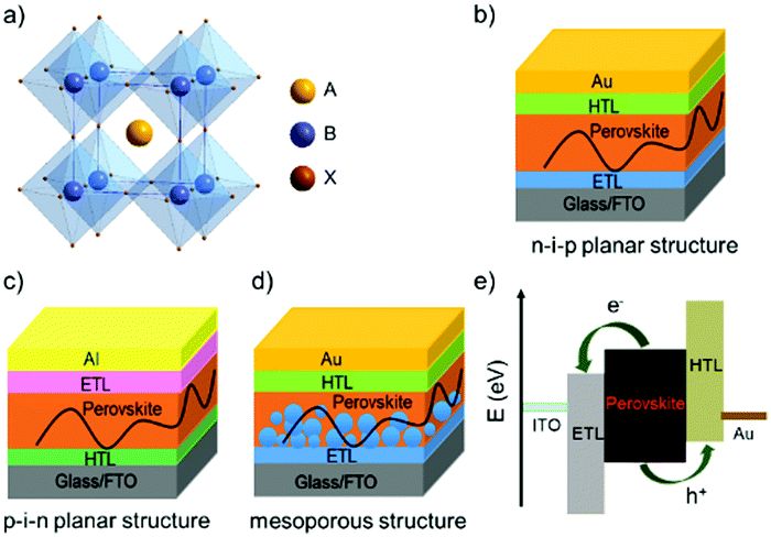 | ||
| Fig. 1 (a) Illustration of a crystalline structure of perovskite ABX3, A: MA+ or FA+ cation, B: Pb2+ cation, X: Cl−, Br− or I− anion. Typical perovskite solar cells with (b) n–i–p structure, (c) p–i–n structure, and (d) mesoporous structure. (e) Energy level scheme for the transporting direction of electron and hole carriers in n–i–p perovskite solar cells. | ||
Depending on the light incidence, PSCs can be broadly divided into either n–i–p or p–i–n architectures, where n- and p- refer to n-type and p-type charge carrier transporting materials, respectively, and i refers to the perovskite optical absorption layer. This definition is also based on the fact whether the electron transporting layer (ETL) or the hole-transporting layer (HTL) is designed to contact with the transparent conductive substrates. For example, in a conventional planar PSC, an ETL can be deposited on the transparent-conductive oxide (TCO) layer such as fluorine-doped tin oxide (FTO) or indium tin oxide (ITO) which will function as the cathode, and then a perovskite layer is prepared on top of the ETL using spin-coating or vacuum evaporation processes. This is then followed by the successive deposition of an HTL and a metal electrode, such as Au or Ag, to form an n–i–p structured device (Fig. 1b).5–9 In contrast, in an inverted PSC design, the positions of the ETL and HTL are simply exchanged (see Fig. 1c).10–14
Compared to the planar n–i–p structured PSCs, the mesoporous PSCs utilize a compact TiO2 layer formed on FTO or ITO substrates and then an additional mesoporous TiO2 layer is deposited as both the ETL and structural scaffold.15–17 Afterwards, the perovskite layer is deposited to form the absorber layer followed by fabrication of the HTL (2,2′,7,7′-tetrakis-(N,N-di-p-methoxyphenylamine)-9,9′-spiro-bifluorene (spiro-OMeTAD) or poly[bis(4-phenyl)(2,4,6-trimethyl-phenyl)amine] (PTAA)) and metal electrode (Fig. 1d). A special feature for the mesoporous structured PSCs is that the mesoscopic transport layer offers large contact areas and interfacial roughness for perovskite layer deposition. Consequently, different outcomes of photocurrent hysteresis and output photovoltage for the planar and mesoporous structured PSC devices can be realized.
One of the key figures of merits for the PSC technology is that the devices can be fabricated using low-temperature solution-processed methods such as spin-coating and screen-printing, which can be easily mass-produced in industry. Upon being irradiated by sunlight, electron–hole pairs (i.e., excitons) are generated in the light-harvesting perovskite layer. After separation of the electron–hole pairs (induced by thermal energy due to a low exciton binding energy), the photo-generated electrons are transported to the conduction band of the ETL, and the holes are transported to the highest occupied molecular orbital (HOMO) energy level of the HTL, and are then collected by the cathode and anode, respectively (in Fig. 1e).18,19
1.1 Brief development of perovskite solar cells
The organic–inorganic metal halide perovskite materials (MAPbI3) were firstly utilized as both a sensitizer and light absorber in solar cells by Miyasaka et al. in 2009,20 though with a low photoelectric PCE of 3.8%. In 2011, Park et al. utilized MAPbI3 perovskite quantum dots (size of 2–3 nm) as the pigment in sensitized solar cells, achieving a high PCE of 6.5%.21 They reported that the light absorption coefficient of the MAPbI3 nanocrystals is one order of magnitude higher than that of the conventional dye, thus MAPbI3 could be effectively used in solid-state sensitized solar cells. In this type of solar cells, a much thinner TiO2 layer (∼2 μm) is widely used. More importantly, a new solid-state mesoscopic solar cell has been developed which can prevent liquid electrolytes from dissolving perovskite, and thus improve its stability.22 In 2012, Park et al. reported ∼10% efficiency for perovskite-based solid-state solar cells by adopting small molecular spiro-OMeTAD as the HTL to replace the iodide-based liquid electrolyte.23 Furthermore, Snaith et al. reported that utilization of an Al2O3 mesoporous layer as the scaffold for the PSCs could achieve much faster electron transport with the perovskite layer, if compared with that using the n-type TiO2 with the perovskite layer.24 Later, a simplified planar structured PSC was successfully developed with the help of the bipolar carrier transport property of perovskite compounds.25Fig. 2 summarizes the key development milestones for the PSCs. For the MAPbI3 perovskite film, a sequential deposition via a two-step dip coating process was developed as one of the effective methods to achieve efficient solution-processed photovoltaic cells with a good reproducibility.26 Park et al. found that the deposition procedure (e.g., one-step27 and two-step coating methods28) of the perovskite layer changes not only the electron lifetime but also the film morphology, which plays a critical role in device performance. Afterwards, the PCE for small-area perovskite devices (∼0.1 cm2) increased rapidly to above 25% within 10 years. However, when the device size increases up to ∼800 cm2, the PCE of PSCs is decreased to 11.6%.29 which is much lower than that of silicon-based solar cells (∼26.7%).30,31 This indicates that the scalability is a crucial issue for the successful commercialization of the PSCs.
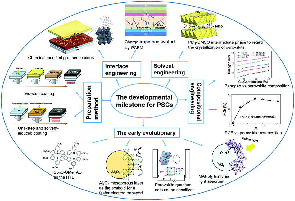 | ||
| Fig. 2 Illustration of the developmental milestones for perovskite solar cells, modified from ref. 24, 29, 38, 42 and 44. | ||
In order to enhance the PSCs' stability in operational conditions and reduction in production costs, various key factors controlling the charge carrier collection within the charge transport layers and their contacts to the absorber layers have been extensively investigated.19 In order to achieve their high efficiencies, the PSCs inevitably require an optimized carrier transport pathway that leverages all of the device layers and their corresponding interfaces. In this regard, interface engineering32–34 has become an effective strategy to tune the optoelectronic properties of the solar cell devices. So far, different methods, such as Lewis base passivation35 and fullerene passivation,36 have been demonstrated to significantly improve solar cell efficiency. For example, the PbI2 (Lewis acid) tends to have strong interactions with those sulfur, oxygen, or nitrogen contained polar aprotic solvents (Lewis base),37 including dimethyl sulfoxide (DMSO),38N,N-dimethylformamide (DMF)39 and N-methylpyrrolidone.40
Although MAPbI3 has been widely used as an active layer in PSCs, it has some disadvantages such as unstable crystalline phases under high humidity and within the solvents. These problems could be solved by using the solvent engineering methods. For instance, a mixed solvent of γ-butyrolactone and DMSO leads to extremely uniform and dense perovskite layers via a CH3NH3I–PbI2–DMSO intermediate phase, and thus enables the fabrication of solar cells with a remarkably increased PCE of 16.2% and without photocurrent hysteresis.41 An absorber based on Cs0.25FA0.75PbI2.40Br0.60 was reported to have a PCE of 17.5% with both good stability and reproducibility.42,43 Seok et al. applied the compositional engineering methodology to develop a (FAPbI3)0.85(MAPbBr3)0.15 perovskite solar cell and achieved a high PCE of 19.0%, which would bring balance between electron and hole transports within the perovskite layer.44
1.2 Charge transport in perovskite solar cells
Fig. 3a presents a scheme of a heterojunction formed among the ETL/perovskite layer/HTL, and Fig. 3b shows the representative development progress of ETLs in the n–i–p architecture. The ETL (usually highly doped n-type metal oxides, donated as n+) must possess a high electron concentration to conduct the electrons to the cathode with a small voltage drop. Under a given bias voltage across the device terminals, the electrical current through the ETL/perovskite and perovskite/HTL contact interfaces must be the same as those of the rest of the device. Therefore, the competition between charge carrier recombination and charge transport is critical for the PSCs which have a typical total thickness of about sub-micrometre. It becomes critical how to further reduce charge carrier recombination at interfaces between ETL/perovskite, and choose the best contact electrode for the PSC devices. | ||
| Fig. 3 (a) Schematic diagram and energy band of interfaces among the electron transport layer (ETL)/perovskite/hole transport layer (HTL). (b) The representative progress of ETLs in the n–i–p architecture. | ||
Highly efficient PSCs generally possess a common feature of two interfaces, e.g., ETL/perovskite interface and HTL/perovskite heterojunction interface, both of which enable efficient charge separation and collection. Fig. 4 illustrates various charge carrier kinetics at these two interfaces, including charge transfer, charge carrier collection and charge carrier recombination. The desirable processes include: (1) photo-excitation in the perovskite; (2) electron transfer to the ETL; and (3) hole transfer to the HTM (or, equivalently, electron transfer from the HTM to the perovskite). The undesirable processes include: (4) bulk recombination of photo-generated species; (5) back charge transfer at the interfaces of TiO2, and (6) charge transfer at the HTM with the perovskite; and (7) charge transfer between TiO2 and the HTM (this may occur if perovskite is absent in some areas, for example, when nanoparticles or voids are present). For achieving high-performance PSCs, processes (4)–(7) must be performed on much slower timescales than charge generation and extraction processes (1)–(3). The interface recombination (non-radiative process) occurs at the ETL/perovskite or perovskite/HTL interface; it is also often called the free-carrier recombination (bimolecular recombination) and can be experimentally verified by investigating the slope of VOCversus light intensity. For efficient planar PSC devices, a slope of lower than 1 kT/q (being 0.0256 dec−1 at room temperature) has been frequently observed.45
 | ||
| Fig. 4 Diagram for charge transfer, collection and recombination of planar PSCs with a structure of ITO/ETL/MAPbI3/HTM/Au. Photon exciton (1), charge transfer (2 and 3), collection and recombination (4, 5, 6, 7) steps take place at the interfaces. The thick green and thin red arrows respectively indicate the processes desirable for energy conversion and those associated with losses. hf, photon energy. | ||
The ETLs in PSCs play important roles in collecting and transferring charge carriers after the injection of electrons from a perovskite active layer, more importantly, realizing effective charge separation and suppressing charge carrier recombination. An inefficient charge transport could cause inhomogeneous charge accumulation and serious interfacial recombination at the ETL/perovskite interface. Therefore, it is highly desirable to design and fabricate ETLs with a high quality in order to guarantee an efficient charge transport in the layer and thus effective photovoltaic performance of devices.
Indeed, each layer (its crystallinity and quality) and the interfacial properties between different layers are critical to achieving highly efficient PSCs.46–49 This can be significantly documented with several critical progresses on perovskite devices and the relative topics.20,23 This article covers the cutting-edge research areas, recent development, critical issues and future directions of ETL materials for PSC applications, with a focus on the following major topics: the functions and requirements of the ETL, and the techniques utilized in the characterization of the ETL. Herein, we briefly discuss the recent advances in design methodology, mechanism and characterization of ETLs. We also analyse ETL material properties including their composition and morphology. We believe readers can also obtain interesting and informative knowledge from different sources in this community.50–53
2. Functions and requirements of electron transport layers
Recently, there have been extensive studies to search for effective ETLs to be used in planar PSCs to further increase charge carrier transport. The main reason is that the VOC values (in the range of ∼1.0–1.2 V) of most PSCs made from organic–inorganic halide lead perovskites are not large enough compared to the typical optical bandgap (between 1.59 and 1.63 eV) of the light absorber. The open circuit losses in the PSCs are mainly due to the recombination occurring in the perovskite bulk layer, and at either the perovskite/transport layer interfaces or the transport layers. Furthermore, the ETL plays critical roles in increasing the power conversion efficiency and life-time of the devices. Usually, such charge carrier contact layers are composed of metal oxide nanocrystals, such as ZnO, TiOx, or doped metal oxides, such as Cl-doped TiO2 (in Fig. 3b).54 A reliable method for producing large-area ETLs is one of the pre-requisites for successful commercialization of the PSC technology. Still, we have to mention the importance of ETL in n-i-p structured PSCs has been long overlooked not only in the preparation procedures of devices but also augments of the performance, mainly due to its thin thickness property (less than 100 nm) and difficulty of controlling the morphology. This is also happened for the HTL in p-i-n structured PSC devices.The mechanism for charge transfer through metal oxide semiconductor nanocrystalline particles and surface charge carrier recombination is illustrated in Fig. 5a, along with a charge injection–accumulation–diffusion model for charge transfer dynamics of those semiconducting nanocrystals, as shown in Fig. 5b. It is clear that defect states in these nanocrystals play a critical role in the charge transport process (capture and release processes). Due to the influence of trap-detrap from defect states, the conductivity of nanocrystals is generally lower than that of the crystalline film. Therefore, electron transport and conductivity mechanisms in metal oxide nanocrystals will significantly influence the efficiency of energy photo conversion in such types of photovoltaic devices.
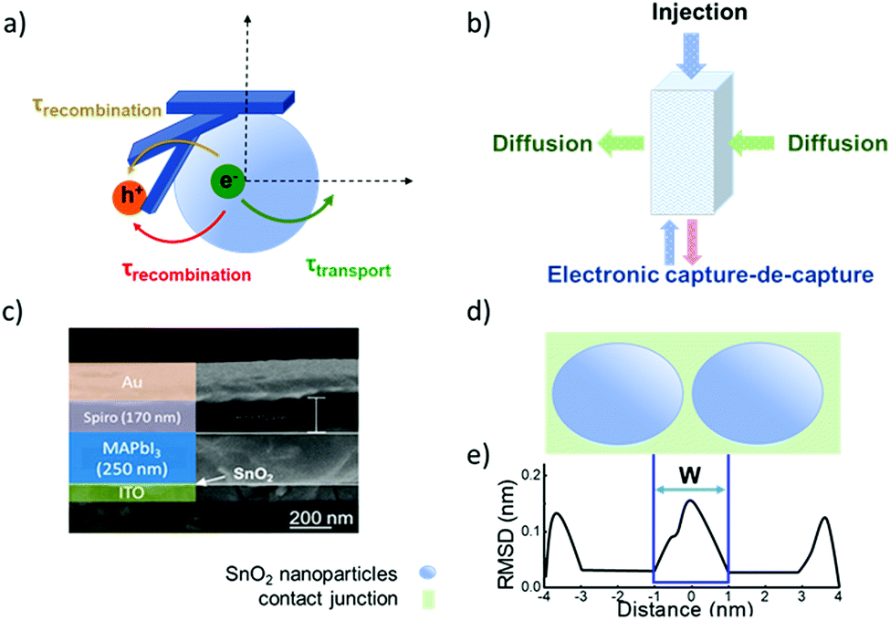 | ||
| Fig. 5 (a) Schematic illustration of the electronic accumulation–diffusion model on a nanocrystalline particle. (b) Effect of defect states in nanocrystalline materials on charge transport. (c) The cross-sectional scanning electron microscope (SEM) image of a planar ITO/SnO2/perovskite/spiro-OMeTAD/Au device. (d) Contact junction (green) of nanocrystalline SnO2 nanoparticles (blue). Molecular dynamics simulation results of two ∼4 nm particles. (e) Average atomic root-mean-squared deviation (RMSD) relative to SnO2 particles in figure d. (c) Reproduced with permission from ref. 55. Copyright 2017 American Chemical Society. | ||
A nanocrystalline metal oxide film can be modelled as a network of junctions formed from the connected nanoparticles. Fig. 5c shows a cross-section scanning electron microscope (SEM) image of a typical planar ITO/SnO2/MAPbI3/spiro-OMeTAD/Au PSC. The charge transport layer thickness is ∼40 nm.55 A fluctuation-induced tunnelling conductivity (FITC) mechanism has been proposed for the charge transport in nanoporous metal oxides such as TiO2 and SnO2, and the charge transport in these films is strongly dependent on the properties of the junctions linking these nanoparticles.56 The FITC model describes contact junctions of these nanoparticles as effective potential energy barriers for transferring electrons, owing to the intrinsic disorder of the semiconductor material between the nanocrystalline particles (Fig. 5d and e).
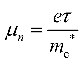
For photovoltaic device applications, the mobility of electrons in the ETL must be high enough to increase the electronic conductivity. Electron mobility (μe) can be expressed using eqn (1):
 | (1) |
| σ = nDE | (2) |
High-quality ETLs should have the following properties: (1) a suitable lowest unoccupied molecular orbital (LUMO) energy level to match with the conduction band energy of perovskite materials, together with good capabilities for electron injection and transportation at the interfaces; (2) high electron mobility (>2.5 × 10⁻⁵ cm2 V−1 s−1), high electrical conductivity (>4 × 10⁻⁶ S cm−1) and photochemical stability under ultraviolet light; and (3) conformal, uniform and pinhole-free film morphology with a low root-mean-square roughness.59 It should be noted that the above criteria for the parameters are for the optimised and highly efficient perovskite photovoltaic devices with low series resistance and high shutting resistance.
A suitable ETL should be also optically transparent to guarantee maximum light absorption by the perovskite layer in the n–i–p PSC. This hinders the choice of suitable materials. For example, some organic materials might have problems with good transparency. The most popular inorganic ETLs are transition metal oxides such as TiO2,60 ZnO,46 and SnO2.61 Although the PSC devices using a TiO2 ETL have achieved a relatively high efficiency (e.g., above 20%), this metal oxide exhibits some drawbacks such as low electronic conductivity and charge transport.62,63 Hence, ZnO and SnO2, well known for their higher electron mobility (bulk mobility: 205–300 cm2 V−1 s−1![[thin space (1/6-em)]](https://www.rsc.org/images/entities/char_2009.gif) 64 and 240 cm2 V−1 s−1,63 respectively) than that of TiO2 (bulk mobility: 1 cm2 V−1 s−163), have emerged as promising ETLs. Last but not least, the stability of the ETL in the PSC devices under operation conditions is also critical for the commercialization of this technology. During the operation of PSCs, ETLs should effectively transport electrons from light absorption layers and prevent hole migration in the direction of electron migration.
64 and 240 cm2 V−1 s−1,63 respectively) than that of TiO2 (bulk mobility: 1 cm2 V−1 s−163), have emerged as promising ETLs. Last but not least, the stability of the ETL in the PSC devices under operation conditions is also critical for the commercialization of this technology. During the operation of PSCs, ETLs should effectively transport electrons from light absorption layers and prevent hole migration in the direction of electron migration.
3. Characterization techniques utilized for the ETL in perovskite solar cells
3.1 Ultrafast spectroscopy characterization
There are several methods available to characterize the charge carrier collection dynamics related to the ETLs such as the electron transport in this layer and interfacial charge carrier recombination at the ETL/perovskite junction. Nanosecond transient absorption spectroscopy (ns-TAS) has been used in order to understand charge injection at the ETL/perovskite interface. For example, photobleaching (PB) negative and photoabsorption (PA) positive peaks of the MAPbI3−xClx based PSCs are usually observed at around 760 and 500–600 nm, respectively. The PB negative peak located at 760 nm can be linked to the band gap or exciton transition of the MAPbI3−xClx film, whereas the PA positive peak at about 500–600 nm is attributed to the absorption of transient species.45,65 When the MAPbI3−xClx was coated on an ETL substrate, an obvious decrease of the peak intensity (i.e., bleaching) was observed at about 760 nm.33 The kinetic decay of photo-bleaching features can be described using a single exponential function, which has a time constant τTAS being related to the excited-stated decay in the perovskite layer. This phenomenon well supports the result obtained from the steady-state PL quenching experiments, which confirms that the ETL contributes to the exciton transition or charge extraction process from the MAPbI3−xClx film.66Electron transport in the nano-crystalline metal oxide ETL can also been characterized using intensity modulated photocurrent spectroscopy (IMPS).67 Using small sinusoidal modulation optical signals, the IMPS could help analysis of transient photoelectric current and transient photovoltage response curves, as well as the characteristic parameters related to carrier transport dynamics such as electron diffusion coefficient and electron lifetime.68 This enables the study of electronic transport under steady state conditions for the photocurrent flow and occupation of electronic states.
3.2 Electronic impedance spectroscopy characterization
Electronic impedance spectroscopy (EIS) is a powerful tool to characterize the electronic and electrical processes in the PSCs, including charge extraction, diffusion and recombination in a thin layer or in the whole device.69 As an example, typical impedance spectra of a PSC using the device structure of FTO/compact TiO2/mesoporous TiO2 (MAPbI3)/spiro-OMeTAD/Au at different bias are shown in Fig. 6.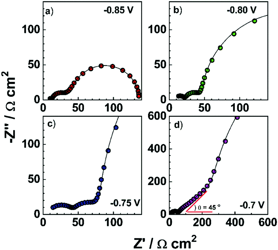 | ||
| Fig. 6 Impedance spectra of a PSC with FTO/compact TiO2/mesoporous TiO2(MAPbI3)/spiro-OMeTAD/Au structure using mesoporous TiO2 (∼20 nm diameter, 800 nm thickness) film as a photo-anode filled with MAPbI3, obtained under dark conditions with different bias: (a–d) Nyquist plots (−0.85, −0.8, −0.75, and −0.7 V, respectively). | ||
In this measurement, the injected electrons from the FTO/TiO2 compact contact are transported through mesoporous TiO2, and then diffuse within the CH3NH3PbI3 and spiro-OMeTAD, eventually reaching the metal counter electrode (Fig. 7a). Frequency analysis showed three distinct frequency ranges (e.g., a high-frequency one at hundreds kHz, a medium-frequency one at hundreds Hz, and a low-frequency one less than Hz). As shown in Fig. 7b, the first arc feature in the high frequency of the Nyquist plot is assigned to the spiro-OMeTAD/Au electrode interface and/or ETL/FTO interface (usually for the bias > −0.85 V). It should be noted that this arc would disappear if the interface is Ohmic contact, thus the presence of an arc indicates the formation of a Schottky junction at this interface. The second arc in the intermediate frequency range is assigned to the interfacial recombination at the ETL/perovskite interface and perovskite/HTL interface, which usually exponentially increases as the bias is decreased. These processes on both interfaces are sometimes difficult to be distinguished due to their similarity. In this frequency region, a Warburg impedance feature might show up which is linked to hole transport (Fig. 6a and b). Instead, a linear Warburg impedance feature appears in the middle frequency range when the bias is decreased from −0.75 to −0.5 V. (Fig. 6c and d). This particular feature arises from an increase in the electron resistance of the (mesoscopic) TiO2 thin film due to the decrease of electron concentration upon decreasing the forward bias. The gradual appearance of charge diffusion in semiconducting materials is correlated with the semi-conductive properties of both the HTL and ETL used in the PSCs. This is a typical behaviour for semiconducting materials when the electronic Fermi level is far from the conduction or valence band energy.70 In this case, the charge carrier transport resistance can be used to obtain the electron/hole diffusion coefficient and mobility based on the three-channel transmission line impedance model (Fig. 7c and d).71 The third arc observed at the low frequency range corresponds to the charge transport in the perovskite layer, such as ion migration. It should be noted that a typical impedance spectrum in Fig. 7b is usually observed in the PSCs using a mesoporous charge transport layer. The features of charge transport in selective layers for the planar PSCs, in which very thin ETLs are used (i.e., low electronic resistance), become invisible by suitably tuning the bias during characterization using impedance spectroscopy.
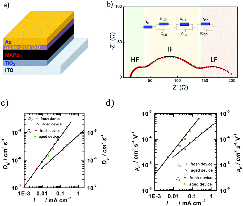 | ||
| Fig. 7 (a) A PSC using a device structure of ITO/TiO2/MAPbI3/spiro-OMeTAD/Au. (b) Typical impedance spectroscopy (Nyquist plot) of this device and the corresponding equivalent circuit, in which HF indicates high frequency, IF indicates intermediate frequency, and LF indicates low frequency. (c and d) The diffusion coefficient and the mobility of holes (left coordinate) and electrons (right coordinate). | ||
The properties of electron transport in the ETL and hole transport in the HTL can be obtained by fitting the impedance spectroscopic data of ITO/TiO2/MAPbI3/spiro-OMeTAD/Au devices. For example, using EIS, we have estimated the hole mobility of a spiro-OMeTAD layer to be about 6 × 10⁻⁴ cm2 V−1 s−1, higher than the electron mobility of TiO2 (∼8 × 10⁻⁵ cm2 V−1 s−1).72,73 Snaith et al. pointed out that the hole mobility of spiro-OMeTAD is higher than the electron mobility of TiO2 through testing the conductivities of the in-plane ‘hole-only’ and ‘electron-only’ devices based on the TiO2 and the spiro-OMeTAD, respectively. The hole conductivity is approximately three times higher than the electron conductivity, with the hole and electron mobilities being 3 × 10⁻⁴ cm2 V−1 s−1 and 0.8 × 10⁻⁴ cm2 V−1 s−1 for spiro-OMeTAD and TiO2, respectively.74 The effective diffusion coefficient of electrons for the TiO2 nanocrystal decreases with the illumination intensities. In the meantime, the diffusion length is shorter than the film thickness. The results show that a reduction of electron transport resistance (for example, by reducing the film thickness, or by increasing the electronic mobility and/or free number of electrons) can significantly improve the PSCs' performance.75 This is realized through tuning of the structural and electronic properties at an atomic level of the ETL for thin film perovskite devices with a total thickness of about 600 nm. However, it is a huge challenge to integrate thin ETL films with other materials into one single electronic device, within a large area and with a sufficient yield. Additionally, the stability issues of PSCs might not be caused by the charge transporting layers.
3.3 Transient decay technology
Transient photo-voltage/photo-current decay (TPV/TPC) measurements can provide useful information on charge transfer properties of the dye-sensitized solar cells, organic solar cells and PSCs.76,77 For the PSCs, there might be different schematic diagrams of electron energy levels based on the device structures. For example, Green et al. suggested an energy-band diagram as shown in Fig. 8a,78 which was based on electron-transfer processes in perovskite nanoparticles and the HTL/perovskite/TiO2 device.79Fig. 8b shows a modified version of the band diagram for the commonly used structure of PSCs in which the electron affinities and band bending in the ITO and SnO2 ETL have been omitted.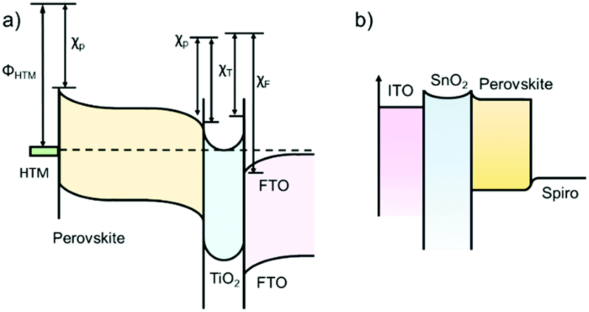 | ||
| Fig. 8 (a) Energy-band diagram deduced from the vacuum energy levels. χP, χT and χF represent the electron affinities of the perovskite, TiO2 and FTO layers, respectively, and ΦHTM represents the work function of the HTM layer. (Modified from ref. 78.) (b) The simplified energy-band diagram for the planar structured PSC. | ||
Similar to EIS measurements, it is impossible for the transient measurements to provide information about the chemical properties of charge carrier species and interfacial recombination. However, the dominant electron transfer process in the device can be experimentally determined by tuning the charge collective layer. This is actually quite useful not only for the transient measurement but also for impedance characterization. For example, by tuning the charge collective layer in the PSCs, it is highly possible to distinguish the contribution from either the ETL or HTL. Fig. 9a and b illustrate the transient photovoltage decay and transient photocurrent decay measurement principles and the corresponding voltage decay signals for the PSCs.80
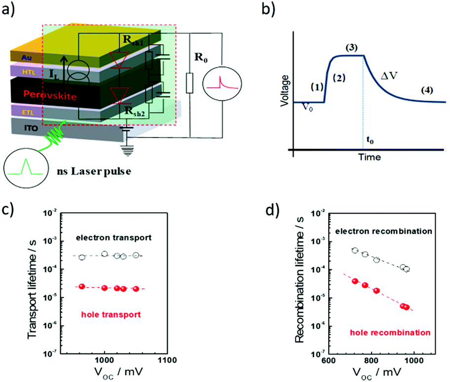 | ||
| Fig. 9 (a and b) The working scheme of transient photovoltage/photocurrent decay measurement. (b) Shows transient photocurrent decay data for an example device. (c) Transport lifetime and (d) recombination lifetime results from using bi-exponential fitting of the transient photocurrent decay and transient photovoltage decay, respectively. | ||
The idea of photo-transient measurement is to use a light transient of small amplitude to probe the device that is under equilibrium conditions, and then monitor the decay kinetics. In practice, this can be achieved by using a short-pulsed laser as a probe to generate a voltage perturbation about the VOC of the cell under the white bias light produced by an array of white light emitting diodes and measuring the voltage decay process thereafter (under open circuit conditions). Specifically, a bias lamp is used for the PSC to maintain bias irradiation with a steady state voltage, V0 (Fig. 9b(1)). Incident red light is superimposed with the previous white light under open-circuit conditions, which boosts the voltage, V = V0 + ΔV, (Fig. 9b(2) and (3)). The red light is turned off at t = t0. Then the photovoltage begins to decay, and returns to the steady state (Fig. 9b(4)). In this case, all the charge carriers generated by the light pulse are assumed to be recombined. When it is excited with a short pulse of light (as short as nano-seconds for the measurement of the PSCs), the photo-generated charges are extracted on the electrodes, thus resulting in a current which can be detected using an oscilloscope in the form of voltage across a resistor (under short circuit conditions). In this case, all the charge carriers generated by the light pulse are assumed to be collected. Transient photocurrent decay measurements are generally conducted under short circuit conditions and provide information about extractable charges, charge recombination and density of states.
In order to precisely obtain the carrier transport parameters based on the photocurrent/photovoltage decay measurements, it is critical to consider the energy band bending effect at the junctions in the PSC devices, i.e., in short circuit or open circuit situations. Fig. 10 shows the electron energy levels of the conduction band and valence band during the transient decay measurements, in which the Fermi levels for an electron in the ETL (and for hole in the HTL) and in the perovskite layer are equal under open circuit conditions for photovoltage decay measurements. However, there is a band-bending for the electron energy levels in the ETL, HTL and perovskite layers in the case of short circuit conditions. The Fermi levels for electrons in the ETL and holes in the HTL for the case under open circuit conditions are different from those in the short circuit case. Therefore, either a bias of voltage or current is needed to apply onto the device to offset the photovoltage/photocurrent produced by steady-state illumination during the transient photovoltage/photocurrent decay measurements. When using this transient decay technique to characterize the PSCs, the bi-exponential decay trends of transient photovoltage and transient photocurrent can often be observed for the signals of electron/hole transport or recombination lifetimes (Fig. 9c and d).
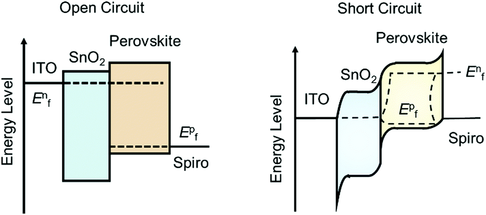 | ||
| Fig. 10 Electron energy levels at open circuit (left) for the transient photovoltage decay measurement and at short circuit (right) for the transient photocurrent decay measurement on a PSC using SnO2 and spiro-OMeTAD as ETL and HTL. The dotted lines indicate the Fermi level of electrons and holes in the perovskite layer. | ||
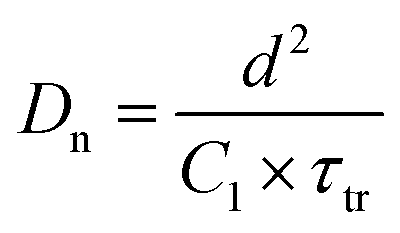
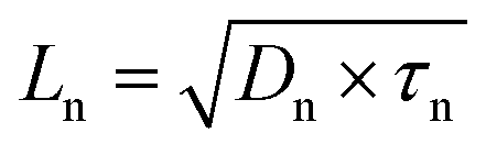
Combining the energy-band diagram shown in Fig. 10 and the ambipolar transport properties of perovskite, we suggested electron/hole transport or recombination lifetimes are the key characteristics of electrons and holes at different time scales.81 For example, the electron and hole diffusion lengths were reported to be 177 nm and 813 nm for the FAPbI3 (FA = HC(NH2)2), whereas a mixed-ion perovskite (MAPbI3−xClx) has shown an opposite situation and they were 1069 nm and 1213 nm for electrons and holes, respectively.82 This indicates that electrons and holes are transported at different rates in this ambipolar material and they have different surface recombination velocities. This is easily understood because the ambipolar material (e.g., perovskite), electron transporting layer (SnO2 or SnS2) and hole transporting layer (spiro-OMeTAD) all possess different electron affinities as discussed above. This can result in different charge transport properties and thus they have different charge transfer lifetimes and recombination lifetimes.83 Therefore, by performing transient photovoltage/photocurrent decay characterization in sub-nanosecond scales at an open-circuit/short circuit, the charge carrier recombination lifetime (τn) and transport lifetime (τtr) at the ETL and HTL for electrons and holes can be empirically evaluated by fitting the obtained transient signals.84,85
The mobilities of electrons and holes for the ETL and HTL are different due to the difference in their surface states, which is dependent on the materials used in the system. For instance, for the PSCs with the ETL using SnO2 or TiO2 and HTL using spiro-OMeTAD doped with Li salt (lithium bis(trifluoromethanesulfonyl)imide) and TBP (4-tert-butylpyridine), the hole mobility was found to be slightly higher than that of electrons.86 The transient photocurrent decay signals can be fitted bi-exponentially, and a shorter transport lifetime corresponding to the holes and a longer transport lifetime corresponding to the electrons could be easily obtained. The recombination lifetime could be also caused by the difference in the numbers of carriers during their recombination. We reported that the short lifetime was related to the charge carrier recombination at the perovskite/spiro-OMeTAD interface, whereas the long lifetime to the charge confined at the perovskite/ETL interface.87 The charge carrier diffusion coefficient can be calculated according to eqn (3):
 | (3) |
 | (4) |
4. Advanced technologies in ETLs for PSCs
4.1 Design rules for ETLs
The specific design rules of ETLs for improving photovoltaic parameters are discussed in this section. Firstly, the J–V curve (in light and dark conditions) of heterojunction PSCs can be described using:88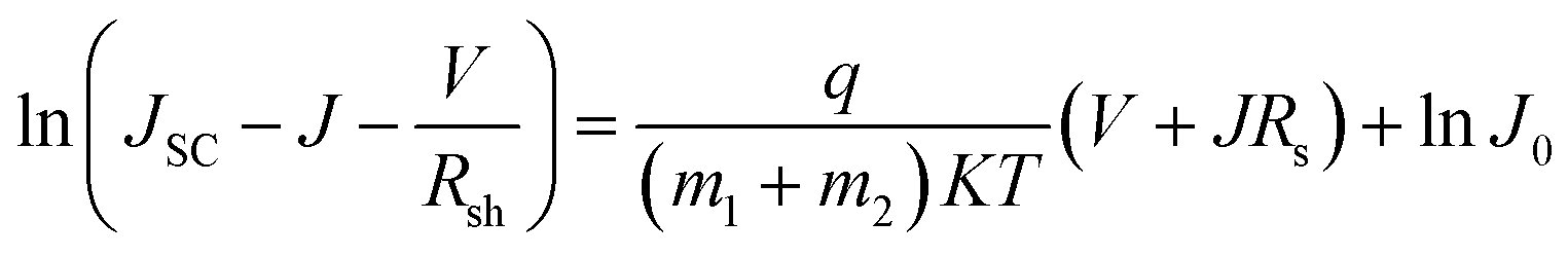 | (5) |
Secondly, the VOC values of PSCs depend on exciton dissociation efficiency, charge transport and the effective density of states according to eqn (6):89
 | (6) |
 | (7) |
Thirdly, the FF of the PSCs is mainly affected by the series resistance Rs of the device and thus a low value of Rs is necessary to eliminate the potential charge loss at high bias voltages and achieve a high FF.91,92 As for the ETL, it is critical to form a smooth surface with less defects, in order to reduce the charge losses and maintain Rs smaller than 5 Ω cm2. Consequently, a high value of FF could be obtained along with a high PCE > 20%. Theoretical analysis based on the Shockley–Queisser efficiency limit showed that the FF for an efficient single junction device can reach as high as ∼90% at room temperature.93
4.2 Electron transport materials in PSCs
Recently, great effort has been made to obtain a high PCE by modifying the ETLs or designing new electron transport materials. In 2015, Liu et al. introduced a self-assembled silane monolayer between the TiO2 and CH3NH3PbI3, achieving optimized interface band alignments and enhanced charge lifetime. The silane monolayer helps tune the interfacial electronic structures and passivate the recombination process, and thus a high efficiency of 12.7% was obtained for a TiO2/SAM/CH3NH3PbI3-based mesoscopic solar cell prepared using a sequential deposition method.94 In 2016, Zuo et al. reported that deposition of various self-assembled monolayers with different functional groups onto the SnO2 surface resulted in chemical interactions within the perovskite layer. The surface trap states were suppressed and the charge transfer at the perovskite/SnO2 interface was enhanced due to the decreased work function and improved interfaces between perovskite and SnO2. The device's efficiency was increased up to 18.8%, showing a 10% improvement compared to that without using the self-assembled monolayer.95 The above work highlights the importance of surface modification and chemical interactions at the perovskite/ETL interfaces, which paves the way for further optimizing ETL development for the PSCs.TiO2 has been used as an ETL due to its suitable energy levels of conduction band minimum (CBM ∼ −3.9 eV) and valence band maximum (VBM ∼ −7.2 eV).75 One of the major disadvantages for the TiO2 ETL is its high processing temperature, which is associated with high costs and unsuitability for flexible PSCs. The electron recombination in the TiO2 ETL is also quite significant due to its inferior electron mobility compared to that of the perovskite, thus resulting in unbalanced charge transfer and consequently poor performance and low efficiency. Moreover, it also suffers from low conductivity and carrier accumulation owing to its numerous trap states.96,97
SnO2 has been regarded as a good ETL material with its advantages including low chemical reactivity and photocatalytic activity,98 a wider band gap of ∼3.8 eV,99 a higher mobility100,101 and a deeper conduction band (−4.3 eV)102 than those of TiO2, which in principle should facilitate more efficient electron transfer from the perovskite. However, most of the devices based on low-temperature solution-processed SnO2 were reported to suffer from serious photocurrent hysteresis which makes it difficult to determine their real PCEs.103,104
The optoelectronic properties of n-type semiconducting ZnO, such as a suitable conduction band energy level (∼−4.17 eV for the CBM), large optical bandgap of 3.3 eV, high electronic mobility and high transmittance, are promising for applications in PSCs.105–107 In addition, the low-temperature processed ZnO nanocrystalline thin films are favourable for flexible devices.64 Nevertheless, ZnO could cause decomposition of organometal halide perovskites, which may impede its large-scale application in PSCs.63
Nb2O5 is a wide bandgap n-type semiconductor with a good chemical stability, an excellent optical transmittance and a higher CBM (−4.33 eV)108 than that of TiO2, which has been applied as an ETL of the PSCs.109,110 For example, Feng et al. deposited amorphous Nb2O5 ETL for large-area rigid PSCs and flexible planar PSCs using an e-beam evaporation method, obtaining PCEs of 18.59% and 15.56%, respectively.111 Moreover, other binary metal oxides, such as WOx112,113 and In2O3,114,115 and ternary metal oxides, such as Zn2SnO4,116,117 BaSnO3118,119 and SrTiO3,120,121 have been proposed for high-efficiency PSCs as listed in Table 1.
| ETL | CBM [eV] | VBM [eV] | Mobility [cm2 V−1 s−1] | Film conductivity [S cm−1] | Ref. |
|---|---|---|---|---|---|
| The labels a, b and c correspond to the references of energy levels (CBM and VBM), mobility and film conductivity, respectively. | |||||
| TiO2 | −4.1 | −7.3 | 1 (bulk) | 1.1 × 10⁻⁵ | 62 c, 63b and 75a |
| SnO2 | −4.3 | −7.9 | 240 (bulk) | 10−3 | 101 c and 102a,b |
| ZnO | −4.17 | −7.47 | 205–300 (bulk) | 1.32 × 10⁻³ | 64 b, 105a and 106c |
| Nb2O5 | −4.33 | −7.79 | 0.2 (bulk) | 2.053 × 10⁻⁵ | 105 b, 108a and 109c |
| WOx | −4.38 | −8.22 | 10–20 (bulk) | 3.4 × 10⁻³ | 112 a,b,c |
| In2O3 | −4.30 | −8.15 | 20 (bulk) | 2.49 × 10⁻⁴ | 114 a,b,c |
| Zn2SnO4 | −4.33 | −7.94 | 10–15 (bulk) | 1.1 × 10⁻² | 116 a,c and 117b |
| BaSnO3 | −3.91 | −7.01 | 300 (bulk) | 10−4 | 118 a,b,c |
| SrTiO3 | −3.65 | −6.90 | 5–8 (bulk) | — | 105 b and 120a |
| SnS2 | −4.24 | −6.54 | 7.85 × 10⁻⁴ (film) | 7.17 × 10⁻⁴ | 58 a,b,c |
| 1-Benzyl-3 methylimidazolium chloride | −4.32 | −8.91 | 1.0 × 10⁻³ (film) | — | 128 a,b |
| TDTP | −4.03 | −5.44 | 4.6 × 10⁻³ (film) | — | 130 a,b |
| PCBM | −4.0 | −6.0 | 2 × 10⁻³ (film) | — | 131 a,b |
| TPE-PDI4 | −3.87 | −5.92 | 1.0 × 10⁻³ (film) | — | 131 a,b |
| N-PDI | −3.72 | −6.05 | — | 0.8 × 10⁻⁵ | 132 a,c |
| PFN-2TNDI | −3.84 | −5.57 | — | — | 143 a |
Based on eqn (2), the free electron concentration is dependent on the charge trapping–de-trapping process via defects in the metal oxide nanocrystals.122 Therefore, an attenuated electron conductivity for most of the conductive metal oxide nanocrystals is usually observed due to the existence of defects inside. Consequently, several strategies have been proposed to increase the conductivity by increasing the number of free electrons and/or diffusion coefficients by doping and alloying engineering.123 For example, doping SnO2 and TiO2 ETLs with metal cations (Y3+, Al3+, Mg2+, In+) has significantly increased the diffusion coefficient to the range of 10−5–10−4 cm2 s−1 and thus has enhanced the electrical conductivity of the ETLs to ∼10−4 S m−1.124–127
Ionic liquids (IL) have also been introduced into PSCs as ETLs or interface modifiers due to their good thermal and electrochemical stability, high electrical conductivity and carrier mobility. For example, Yang et al. used solid state ionic-liquid (ss-IL), (1-benzyl-3 methylimidazolium chloride) as the ETL, prepared using a low-temperature solution process.128 The hydrophilic nature of ss-IL facilitates the formation of high-quality perovskite films with reduced electron trap-state densities. The flexible PSC has achieved a record PCE of 16.09%. Meanwhile, they developed 1-butyl-3-methylimidazolium tetrafluoroborate IL to tailor the surface properties of TiO2, including smoothening the TiO2 surfaces, reducing the work function of TiO2, and improving electron mobility.129 After modification by the IL, the device PCE was increased to 19.62%, and the J–V hysteresis was completely eliminated due to significantly reduced traps and balanced charges.
Recently, many organic small molecules have been developed as the ETLs for highly efficient PSC devices. Compared with their inorganic counterparts, the organic ETLs offer fascinating flexibility of chemistry to react with perovskite compounds and low processing temperature for device fabrication. For example, Gu et al. proposed an n-type sulfur-containing azaacene (TDTP) as the ETL to replace the PCBM in an inverted PSC.130 The sulphur species inside the molecular structures was identified to dramatically improve the interfacial interactions between the ETL molecules and perovskite layer through formation of S–I or S–Pb chemical bonds, thus displaying a high electron mobility of 4.6 × 10⁻³ cm2 V−1 s−1 and passivating the perovskite surface, which enhances the PCE up to 18.2% (Fig. 11a). Jiang et al. synthesized three-dimensional perylenediimide (PDI)-based molecules (TPE-PDI4) with a high electron mobility of 1.0 × 10⁻³ cm2 V−1 s−1. When the TPE-PDI4 was used as the ETL in their study, the obtained PSCs achieved a high PCE of 16.29% (Fig. 11b). Moreover, when used as a thin interfacial layer, the PSCs based on TPE-PDI4 could achieve an efficiency of 18.78%.131
 | ||
| Fig. 11 (a) Molecular structure of TDTP and J–V curves of PSCs with different TDTP thicknesses.130 (b) Chemical structure of TPE-PDI4 and forward/reverse scans of PSCs using TPE-PDI4 and PCBM as ETLs, respectively.131 (c) Molecular structure of N-PDI, EIS curve of PSCs with different ETLs obtained at around VOC under illumination with an LED array emitting white light, the applied voltage of 0.9 V is given, and J–V curves of the perovskite solar cells based on FTO/N-PDI with different thicknesses and the control device based on the FTO substrate.132 Reproduced from ref. 130–132 with permission from the Royal Society of Chemistry. | ||
Besides, a few studies have fully demonstrated the overall advantages of using these organic ETLs, including adjustability of optoelectronic properties by structural changes, availability of multi-defined structures, and easy purification and synthesis in material processing, as well as batch-to-batch reproducibility and flexibility. For example, Zhang et al. introduced an amino-substituted perylene diimide derivative (N-PDI) ETL into the PSCs.132 The interactions between the amino groups of N-PDI and Sn(IV) of the FTO substrate have been found to accelerate the surface electron extraction and passivate the surface trap states of the MAPbI3−xClx film by using the N-PDI (Fig. 11c). Owing to the significant reduction of electron trap density by passivation, a smaller capacitance was obtained from the response in the intermediate frequency region in the EIS results for the N-PDI based device. This decrease in capacitance results in a higher VOC value and boosts the JSC and FF for N-PDI-based devices. As a result, an excellent PCE of 17.66% on the FTO substrate was achieved.132
 | ||
| Fig. 12 Outlines for the design features and development trend of ETLs for the large area and flexible PSCs, including the energetics and work function tenability between the ETL and perovskite layer, the methods for low-temperature fabrication of various functional layers, and the strategies for efficient charge extraction and transport via two-dimensional materials or surface passivation with organic functional groups for instance. | ||
In addition, double-layer ETLs are also used to further improve the charge extraction and passivate the surface defects of the perovskite. For example, TiO2/SnO2 bilayer ETLs can reduce the leakage current and the charge recombination compared with a single ETL of either TiO2 or SnO2.133 Wang et al. found that [6,6]-phenyl-C61-butyric acid (PCBA) could partially fill the surface trap states of SnO2 and passivate the interfaces between SnO2 and perovskite in the SnO2/PCBA-based bilayer PSCs.134 Moreover, a ZnO/fullerenes bilayer ETL could efficiently hinder the reactions between ZnO and the perovskite during annealing (>100 °C), thus improving the device's stability.135
The electron selective layers of perovskite solar cells are also critical for achieving good photovoltaic properties.136 Despite exhibiting a low electron mobility for the a-SnO2 (generally prepared using a sol–gel method), its suitable electronic energies combined with high transparency (Egap > 4 eV) and uniform substrate coverage make it an excellent ETL candidate for the low-cost and large-scale fabrication of organo-halide lead PSCs and other organic photovoltaics. Fig. 12 outlines the design features and development trends of ETLs for large area and flexible PSCs, including the energetics and work function tenability between the ETL and perovskite layer, the method for low-temperature fabrication of various functional layers, and the strategies for efficient charge extraction and transport via two-dimensional materials or surface passivation with organic functional groups for instance.
For example, Shin et al. reported a low-temperature (<180 °C) solution-processed SnO2 ETL prepared using a spin-coating method, which showed good antireflection, suitable band edge positions, and high electron mobility.137 As a result, the planar PSC made using this layer has achieved a PCE of 17.21% with a high VOC value of 1.11 V and a high JSC value of 23.27 mA cm−2 under the reverse voltage scan. Yang et al. applied amorphous TiO2 (am-TiO2) as the ETL, which can be prepared at room temperature using a magnetron sputtering method.138 The film exhibited favourable transmittance and fast electron extraction and transport. The large-area (>10 mm2) and flexible PSCs based on am-TiO2 achieved a PCE of 15.07%. Li et al. recently introduced homogeneous carbon quantum dots (CQDs) into the nanocrystal TiO2 solution to form a high quality ETL for efficient PSCs (Fig. 13a).66 Notably, these CQDs exhibited excellent light harvesting ability and acted as an electron reservoir, thus leading to a significant improvement of efficient charge carrier extraction and injection between the TiO2 and perovskite layer in PSCs. When the amount of CQDs added was 10 wt.%, the planar heterojunction PSC achieved a PCE as high as ∼19% (Fig. 13b). This is mainly attributed to the improvement of electron mobility and electron extraction ability (Fig. 13c), and the good matching of the energy levels between the ETL and perovskite active layer by the adding these CQDs. All of these have led to remarkable increases in both the values of JSC and VOC.
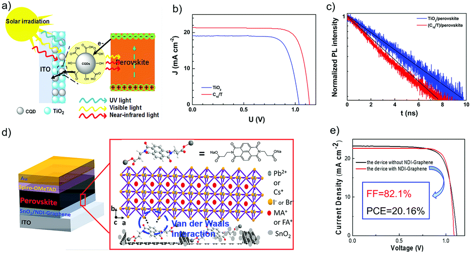 | ||
| Fig. 13 (a) Schematic illustration of the working mechanism for the perovskite with CQD-doped TiO2 as the ETL. (b) J–V curves of PSCs based on ITO/C10/T and the control device based on the ITO/TiO2 substrate. (c) Time-resolved PL decay transients for TiO2/perovskite (black), and CQD-doped TiO2/perovskite (red) films. (d) Schematic architecture of planar perovskite solar cells.66 The expanded scheme shows the chemical structure of NDI and the bonding conditions of NDI-graphene with perovskite films. (e) J–V curve (reverse scan) of device based on SnO2–5% G ETL.141 (a–c) Reproduced with permission from ref. 66. Copyright 2017 American Chemical Society. (d and e) Reproduced from ref. 141. Copyright 2018 American Chemical Society. | ||
The electronic conductivity of SnO2 can also be increased via doping a moderate level of graphene quantum dots (GQDs).139 Therefore, photo-generated electrons transferred from the GQDs to SnO2 could effectively fill electronic traps and thus improve the device's PCE from 17.91% to 20.31% with significantly reduced hysteresis. A further thermal treatment of dispersions of GQDs and SnO2 has been found to improve the film coverage and reproducibility.140
Zhao et al. reported the usage of electronic conducting graphene to form graphene/SnO2 composites, which were then used as an ETL in the PSC (Fig. 13d).141 Van der Waals interactions were generated between the perovskite material and graphene, which were proved to be able to fix the octahedral [PbI6]4− at the perovskite/ETL interface. After optimization, a high PCE of 20.2% and a high FF of 82% have been achieved by using FA0.75MA0.15Cs0.1PbI2.65Br0.35 perovskite and the optimized amount of graphene of 5 v/v%. This good performance has been attributed to the enhancement of electron mobility and extraction ability, and the reduced carrier recombination (Fig. 13e).
Yang et al. mixed ethylene diamine tetra-acetic acid (EDTA) into a SnO2 aqueous colloidal dispersion to prepare an EDTA-complexed SnO2 (E-SnO2) ETL.100 Compared to that of SnO2, this E-SnO2 showed a smaller contact angle with water, thus resulting in the reduced Gibbs free energy for the nucleation of perovskites and lowered surface energy for its growth. All these resulted in the production of high-quality perovskite films. Moreover, the EDTA modification increased the electron mobility by three times, suppressed hysteresis, and improved the VOC value due to an improved energy level alignment against perovskite. A rigid PSC and a flexible PSC with the E-SnO2 as the ETL achieved PCEs of 21.60% and 18.28%, respectively.
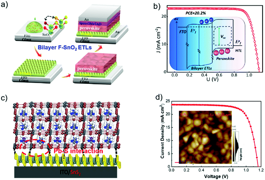
Gong et al. reported the use of F-doped SnO2 (F:SnO2) nanocrystals as the ETL in an n–i–p planar PSC (Fig. 14a), and the device's VOC values could be tailored by gradually changing the band offset at the interface of the perovskite active layer and ETL. The up-shifts of the Fermi level of the new ETL by doping of F− were reported to be around 68 and 95 meV, which are beneficial for free electron extraction and transport. The built-in potential at the ETL/perovskite heterojunction interface was estimated to be 1.06 V, which can effectively decrease the carrier recombination and increase the VOC. Consequently, the n–i–p planar PSC using this bilayer ETL has achieved a PCE of 20.2% with a high VOC of 1.13 V (Fig. 14b).142 Zhao et al. recently demonstrated a new strategy of utilizing a two-dimensional SnS2 as the ETL material for high-efficiency PSCs via a self-assembly stacking deposition method (Fig. 14c). The large-scale two-dimensional multilayer SnS2 sheet structure promoted heterogeneous nucleation over the perovskite precursor film. The intermolecular Pb–S interactions between perovskite and SnS2 could passivate the interfacial trap states, which suppressed charge carrier recombination and thus facilitated electron extraction for balanced charge transport at the interfaces between the electron transporting layer/perovskite and hole transporting layer/perovskite. Based on this design, a PCE value of 20.12% was realized for the 2D ETL based PSCs, along with a high JSC of 23.55 mA cm−2 and an impressive VOC value of 1.161 V (Fig. 14d).58 The proposed SnS2 ETL has many advantages including the simple and convenient process, controllability, and enhanced contacts for charge transfer.
 | ||
| Fig. 14 (a) Flowchart of the fabrication process. (b) J–V curves of PSCs based on bilayer ETL; the inset is the Quasi-Fermi level splitting of the bilayer ETL based devices at open circuit under illumination.142 (c) Illustration of the perovskite films deposited on the SnS2 substrate. (d) J–V curves (reverse scan) of devices A (SnO2 as ETL) and B (SnS2 as ETL), respectively; the inset shows AFM images of a 2D multilayer SnS2 film.58 (a and b) Reproduced with permission from ref. 142. Copyright 2018 American Chemical Society. (c and d) Reproduced with permission from ref. 58. Copyright 2018 Wiley. | ||
Polymer semiconductors possess many appealing features, some of which make them potentially good candidates for the ETL, such as simple process, adjustable energy levels and excellent optical and electrical properties. Generally, a semiconductor oxide can be conveniently dispersed in an organic phase to modify the surface area effect, volume effect and quantum size effect, and thus will lead to low carrier recombination rates. For example, Li et al. reported a copolymer PFN-2TNDI with a conjugated structure as the ETL in PSCs (Fig. 15a).143 The work function of the ITO was reduced to 3.81 eV after the deposition of PFN-2TNDI (5 nm), thus facilitating formation of an ohmic contact and efficient charge transfer and extraction at the ETL/MAPbI3−xClx interface (Fig. 15b). The PFN-2TNDI device showed a good performance with a PCE value of 16%. More importantly, in addition to the low temperature processability offered by the polymer ETL, the devices based on the polymer ETL showed significantly enhanced photostability against UV irradiation (Fig. 15c).
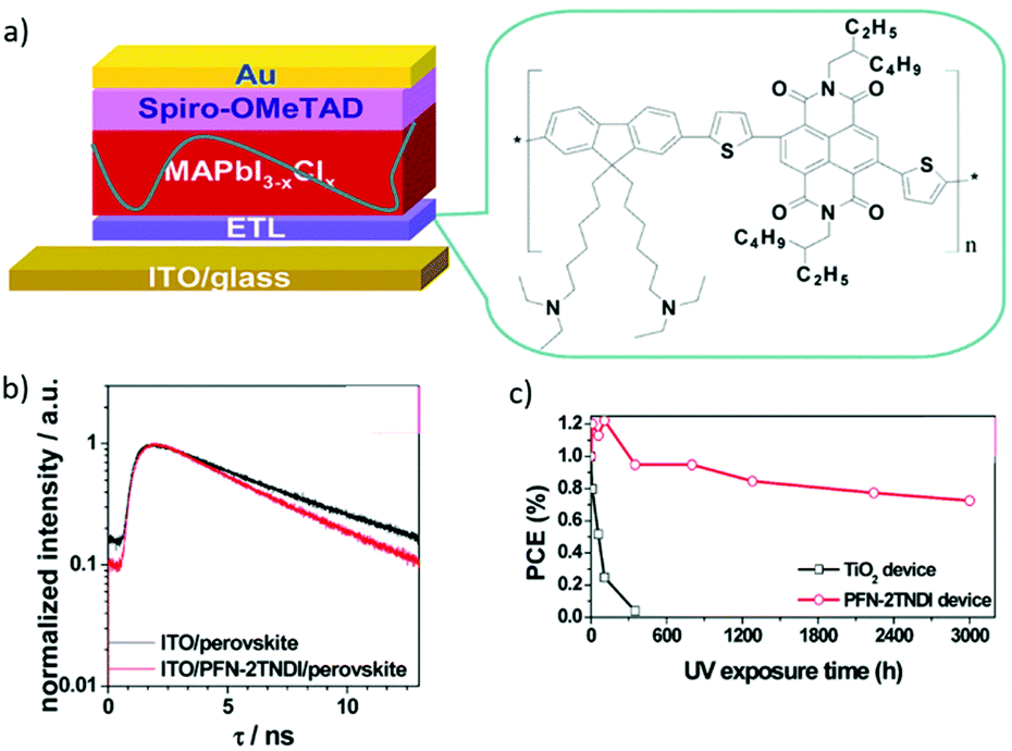 | ||
| Fig. 15 (a) The n–i–p structured planar heterojunction PSCs using the PFN-2TNDI electron transport layer. (b) Time-resolved PL decay of MAPbI3−xClx films on the ITO and ITO/PFN-2TNDI. (c) The evolution of PCE as a function of testing time under UV illumination for the PFN-2TNDI- and TiO2-based PSCs. The devices were stored under exposure to UV in a N2-filled glove-box during testing.143 Reproduced from ref. 143 with permission from the Royal Society of Chemistry. | ||
5. Conclusion and outlook
In this paper, we have comprehensively reviewed recent advances of ETLs based on organic and inorganic structures for highly efficient PSCs (PCE > 20%). Unlike other thin film photovoltaics, production of perovskite solar cells in a large area becomes a significant issue for a successful commercialization, in which the methods of electron transport layers onto the transparent conductive oxide substrates becomes one of technique barriers. As discussed above, specific design methodologies of ETLs have been used to improve the photovoltaic parameters. Various properties (including electrochemical properties and surface morphology properties) of the ETLs have been exploited to enhance the performance of PSCs. An efficient ETL should possess high electron mobility, high electrical conductivity, uniform and pinhole-free film morphology and suitable LUMO energy levels, which should match with those of the perovskites. Besides, ultrafast spectroscopy characterization, electronic impedance spectroscopy characterization, and transient decay technology could provide critical information on carrier dynamics including charge extraction, diffusion and recombination related to the ETLs. With the help of these characterization techniques, significant enhancement of PCEs has been realized by designing new electron transport materials or modifying the ETLs. Metal oxides, for example TiO2, SnO2, and ZnO, are the most widely used as ETLs. Further tailoring of their electrical properties can be realized by doping and alloying engineering or optimizing the surface of ETLs with lower defect density and forming a better contact with perovskites by introducing extra components. In addition, some organic molecules have been developed as electron transport materials.Despite the rapid advances, further optimization of ETLs is critically desired in order to further improve the device efficiency and stability for successful commercialization. For the inorganic metal oxide-based ETLs, their components, synthesis or deposition methods, and post processes could be further optimized, for example, to lower the annealing temperature for crystallization or to optimise the morphology for the enhancement of electron transfer. For the organic ETLs, attention should be paid to the purity and stability under the heating treatment.
As the PSCs have already achieved excellent PCE values over 25%, there should be further investigations for controlling factors and methods for the scaling up of large-area and flexible PSCs. First, it is well-known that the composition of the ETLs can largely impact the design of scalable deposition.29 Developing appropriate ETLs in order to meet the stringent requirements for large-area modules has become one of the crucial research topics. The ETLs should not only have high mobility, high conductivity, smoothness and compact coverage of film morphology and suitable energy level, but also be easily produced at a low-temperature (<150 °C) in order to be compatible with the standard industrial processes as well.144
Secondly, a scalable deposition process should be capable of controlling nucleation and growth of perovskites, which requires advanced equipment and harsh production conditions.145 Strategies could be adopted to reduce fabrication technology requirements. For example, the surface energy and structure of the ETLs could be tailored by functionalizing them with surface-organic groups. Novel two-dimensional ETLs could also be designed in order to control the crystallization kinetics and film quality of perovskites.
Finally, PSCs fabricated using current scalable fabrication methods, including roll-to-roll production, doctor-blade coating and spray-coating, often show low PCEs and poor stability. To overcome such issues, hydrophobic groups such as fluorine and carbon nanotubes can be introduced into electron transport materials, which will not only improve the long-term stability of the PSCs against water, oxygen, light and heat, but also passivate surface defects of the ETLs to enhance the photovoltaic performance.
Conflicts of interest
There are no conflicts to declare.Acknowledgements
The authors acknowledge financial support from the National Key Research and Development Program of China (2019YFE0101300), the Natural Science Foundation of China (NSFC No. 21673091, 51961165106, and 21975088), the NSFC Major International (Regional) Joint Research Project NSFC-SNSF (No. 51661135023, and 51961165106), the Central Universities of Huazhong University of Science & Technology (2018KFYXKJC034 and 2019kfyRCPY040), and the Double first-class research funding of China-EU Institute for Clean and Renewable Energy (3011187029), Newton Mobility (IE161019) through Royal Society and the NSFC. Reproduced from ref. 130–132 and 143 with permission from the Royal Society of Chemistry. SA acknowledges funding from the European Union H2020 Programme under European Research council Consolidator grant [MOLEMAT, 726360].Notes and references
- P. Kung, M. Lin, P. Lin, J. Jhang, M. Pantaler, D. Lupascu, G. Grancini and P. Chen, Sol. RRL, 2020, 4, 1900306 CrossRef CAS.
- P. Li, X. Liu, Y. Zhang, C. Liang, G. Chen, F. Li, M. Su, G. Xing, X. Tao and Y. Song, Angew. Chem., Int. Ed., 2020, 59, 2–8 CrossRef.
- L. Krückemeier, U. Rau, M. Stolterfoht and T. Kirchartz, Adv. Energy Mater., 2020, 10, 1902573 CrossRef.
- H. Ren, S. Yu, L. Chao, Y. Xia, Y. Sun, S. Zuo, F. Li, T. Niu, Y. Yang, H. Ju, B. Li, H. Du, X. Gao, J. Zhang, J. Wang, L. Zhang, Y. Chen and W. Huang, Nat. Photonics, 2020, 14, 154–163 CrossRef CAS.
- J. Yoo, S. Wieghold, M. Sponseller, M. Chua, S. Bertram, N. Hartono, J. Tresback, E. Hansen, J. Correa-Baena, V. Bulović, T. Buonassisi, S. Shin and M. Bawendi, Energy Environ. Sci., 2019, 12, 2192–2199 RSC.
- A. Solanki, P. Yadav, S. Turren-Cruz, S. Lim, M. Saliba and T. Sum, Nano Energy, 2019, 58, 604–611 CrossRef CAS.
- D. Lin, T. Zhang, J. Wang, M. Long, F. Xie, J. Chen, B. Wu, T. Shi, K. Yan, W. Xie, P. Liu and J. Xu, Nano Energy, 2019, 59, 619–625 CrossRef CAS.
- C. Dong, X. Han, W. Li, Q. Qiu and J. Wang, Nano Energy, 2019, 59, 553–559 CrossRef CAS.
- Y. Liu, Q. Chen, H. Duan, H. Zhou, Y. Yang, H. Chen, S. Luo, T. Song, L. Dou, Z. Hong and Y. Yang, J. Mater. Chem. A, 2015, 3, 11940–11947 RSC.
- Z. Liu, K. Liu, F. Zhang, S. Jain, T. He, Y. Jiang, P. Liu, J. Yang, H. Liu and M. Yuan, Sol. Energy, 2020, 195, 436–445 CrossRef CAS.
- J. Yu, S. Badgujar, E. Jung, V. Singh, D. Kim, J. Gierschner, E. Lee, Y. Kim, S. Cho, M. Kwon and M. Song, Adv. Mater., 2019, 31, 1805554 Search PubMed.
- H. Pham, L. Gil-Escrig, K. Feron, S. Manzhos, S. Albrecht, H. Bolink and P. Sonar, J. Mater. Chem. A, 2019, 7, 12507–12517 RSC.
- H. Huang, Y. Shih, L. Wang and K. Lin, Energy Environ. Sci., 2019, 12, 1265–1273 RSC.
- C. Ng, K. Hamada, G. Kapil, M. Kamarudin, Z. Wang, S. Iikubo, Q. Shen, K. Yoshino, T. Minemoto and S. Hayase, J. Mater. Chem. A, 2020, 8, 2962–2968 RSC.
- T. Yang, N. Jeon, H. Shin, S. Shin, Y. Kim and J. Seo, Adv. Sci., 2019, 6, 1900528 CrossRef PubMed.
- F. Li, C. Zhang, J. Huang, H. Fan, H. Wang, P. Wang, C. Zhan, C. Liu, X. Li, L. Yang, Y. Song and K. Jiang, Angew. Chem., Int. Ed., 2019, 58, 6688–6692 CrossRef CAS PubMed.
- X. Shi, Y. Ding, S. Zhou, B. Zhang, M. Cai, J. Yao, L. Hu, J. Wu, S. Dai and M. Nazeeruddin, Adv. Sci., 2019, 6, 1901213 CrossRef CAS PubMed.
- X. Ren, Z. Wang and W. Choy, Adv. Opt. Mater., 2019, 7, 1900407 CrossRef CAS.
- P. Lopez-Varo, J. Jiménez-Tejada, M. García-Rosell, S. Ravishankar, G. Garcia-Belmonte, J. Bisquert and O. Almora, Adv. Energy Mater., 2018, 8, 1702772 CrossRef.
- A. Kojima, K. Teshima, Y. Shirai and T. Miyasaka, J. Am. Chem. Soc., 2009, 131, 6050–6051 CrossRef CAS PubMed.
- J. Im, C. Lee, J. Lee, S. Park and N. Park, Nanoscale, 2011, 3, 4088–4093 RSC.
- M. Liu, M. Johnston and H. Snaith, Nature, 2013, 501, 395 CrossRef CAS PubMed.
- H. Kim, C. Lee, J. Im, K. Lee, T. Moehl, A. Marchioro, S. Moon, R. Humphry-Baker, J. Yum, J. Moser, M. Grätzel and N. Park, Sci. Rep., 2012, 2, 591 CrossRef PubMed.
- M. Lee, J. Teuscher, T. Miyasaka, T. Murakami and H. Snaith, Science, 2012, 338, 643–647 CrossRef CAS PubMed.
- L. Calio, S. Kazim, M. Grätzel and S. Ahmad, Angew. Chem., Int. Ed., 2016, 55, 14522–14545 CrossRef CAS PubMed.
- J. Burschka, N. Pellet, S. Moon, R. Humphry-Baker, P. Gao, M. Nazeeruddin and M. Grätzel, Nature, 2013, 499, 316 CrossRef CAS PubMed.
- M. Xiao, F. Huang, W. Huang, Y. Dkhissi, Y. Zhu, J. Etheridge, A. Gray-Weale, U. Bach, Y. Cheng and L. Spiccia, Angew. Chem., Int. Ed., 2014, 53, 9898–9903 CrossRef CAS PubMed.
- N. Jeon, H. Na, E. Jung, T. Yang, Y. Lee, G. Kim, H. Shin, S. Seok, J. Lee and J. Seo, Nat. Energy, 2018, 3, 682 CrossRef CAS.
- N. Park and K. Zhu, Nat. Rev. Mater., 2020, 5, 333–350 CrossRef CAS.
- K. Yoshikawa, H. Kawasaki, W. Yoshida, T. Irie, K. Konishi, K. Nakano, T. Uto, D. Adachi, M. Kanematsu, H. Uzu and K. Yamamoto, Nat. Energy, 2017, 2, 17032 CrossRef CAS.
- S. Bhattacharya and S. John, Sci. Rep., 2019, 9, 12482 CrossRef PubMed.
- M. Tavakoli, M. Saliba, P. Yadav, P. Holzhey, A. Hagfeldt, S. Zakeeruddin and M. Grätzel, Adv. Energy Mater., 2019, 9, 1802646 CrossRef.
- H. Li, L. Tao, F. Huang, Q. Sun, X. Zhao, J. Han, Y. Shen and M. Wang, ACS Appl. Mater. Interfaces, 2017, 9, 38967–38976 CrossRef CAS PubMed.
- P. Su, L. Liu, H. Yao, T. Liu, B. Zhang, J. Wang, S. Feng, A. Runa, W. Fu and H. Yang, Org. Electron., 2020, 77, 105490 CrossRef CAS.
- X. Cao, L. Zhi, Y. Li, F. Fang, X. Cui, Y. Yao, L. Ci, K. Ding and J. Wei, J. Mater. Chem. C, 2017, 5, 7458–7464 RSC.
- Y. Shao, Z. Xiao, C. Bi, Y. Yuan and J. Huang, Nat. Commun., 2014, 5, 5784 CrossRef CAS PubMed.
- E. Aktas, J. Jiménez-López, C. Rodríguez-Seco, R. Pudi, M. Ortuño, N. López and E. Palomares, ChemPhysChem, 2019, 20, 2702–2711 CrossRef CAS PubMed.
- Y. Wu, A. Islam, X. Yang, C. Qin, J. Liu, K. Zhang, W. Peng and L. Han, Energy Environ. Sci., 2014, 7, 2934–2938 RSC.
- A. Wakamiya, M. Endo, T. Sasamori, N. Tokitoh, Y. Ogomi, S. Hayase and Y. Murata, Chem. Lett., 2014, 43, 711–713 CrossRef CAS.
- Y. Jo, K. Oh, M. Kim, K. Kim, H. Lee, C. Lee and D. Kim, Adv. Mater. Interfaces, 2016, 3, 1500768 CrossRef.
- N. Jeon, J. Noh, Y. Kim, W. Yang, S. Ryu and S. Seok, Nat. Mater., 2014, 13, 897 CrossRef CAS PubMed.
- K. Bush, K. Frohna, R. Prasanna, R. Beal, T. Leijtens, S. Swifter and M. McGehee, ACS Energy Lett., 2018, 3, 428–435 CrossRef CAS.
- C. Zuo, H. Bolink, H. Han, J. Huang, D. Cahen and L. Ding, Adv. Sci., 2016, 3, 1500324 CrossRef PubMed.
- N. Jeon, J. Noh, W. Yang, Y. Kim, S. Ryu, J. Seo and S. Seok, Nature, 2015, 517, 476 CrossRef CAS PubMed.
- X. Shai, J. Wang, P. Sun, W. Huang, P. Liao, F. Cheng, B. Zhu, S. Chang, E. Yao, Y. Shen, L. Miao, Y. Yang and M. Wang, Nano Energy, 2018, 48, 117–127 CrossRef CAS.
- D. Zheng, G. Wang, W. Huang, B. Wang, W. Ke, J. Logsdon, H. Wang, Z. Wang, W. Zhu, J. Yu, M. Wasielewski, M. Kanatzidis, T. Marks and A. Facchetti, Adv. Funct. Mater., 2019, 29, 1900265 CrossRef.
- Z. Wu, Z. Liu, Z. Hu, Z. Hawash, L. Qiu, Y. Jiang, L. Ono and Y. Qi, Adv. Mater., 2019, 31, 1804284 CrossRef.
- Z. Liang, Z. Bi, K. Gao, Y. Fu, P. Guan, X. Feng, Z. Chai, G. Xu and X. Xu, Appl. Surf. Sci., 2019, 463, 939–946 CrossRef CAS.
- H. Pham, L. Gil-Escrig, K. Feron, S. Manzhos, S. Albrecht, H. Bolink and P. Sonar, J. Mater. Chem. A, 2019, 7, 12507–12517 RSC.
- M. Kam, Q. Zhang, D. Zhang and Z. Fan, Sci. Rep., 2019, 9, 6963 CrossRef.
- H. Sun, Y. Zhou, Y. Xin, K. Deng, L. Meng, J. Xiong and L. Li, Adv. Funct. Mater., 2019, 29, 1808667 CrossRef.
- K. Huang, Y. Peng, Y. Gao, J. Shi, H. Li, X. Mo, H. Huang, Y. Gao, L. Ding and J. Yang, Adv. Energy Mater., 2019, 9, 1901419 CrossRef CAS.
- C. Liu, L. Zhang, X. Zhou, J. Gao, W. Chen, X. Wang and B. Xu, Adv. Funct. Mater., 2019, 29, 1807604 CrossRef CAS.
- H. Tan, A. Jain, O. Voznyy, X. Lan, F. Arquer, J. Fan, R. Quintero-Bermudez, M. Yuan, B. Zhang, Y. Zhao, F. Fan, P. Li, L. Quan, Y. Zhao, Z. Lu, Z. Yang, S. Hoogland and E. Sargent, Science, 2017, 355, 722–726 CrossRef CAS PubMed.
- J. Barbé, M. Tietze, M. Neophytou, B. Murali, E. Alarousu, A. Labban, M. Abulikemu, W. Yue, O. Mohammed, I. McCulloch, A. Amassian and S. Del Gobbo, ACS Appl. Mater. Interfaces, 2017, 9, 11828–11836 CrossRef PubMed.
- P. Piotrowiak, Solar Energy Conversion: Dynamics of Interfacial Electron and Excitation Transfer, RSC Publishing, 2013 Search PubMed.
- A. Reshak, RSC Adv., 2014, 4, 39565–39571 RSC.
- X. Zhao, S. Liu, H. Zhang, S. Chang, W. Huang, B. Zhu, Y. Shen, C. Shen, D. Wang, Y. Yang and M. Wang, Adv. Funct. Mater., 2019, 29, 1805168 CrossRef.
- T. Liu, K. Chen, Q. Hu, R. Zhu and Q. Gong, Adv. Energy Mater., 2016, 6, 1600457 CrossRef.
- Y. Zhang, X. Liu, P. Li, Y. Duan, X. Hu, F. Li and Y. Song, Nano Energy, 2019, 56, 733–740 CrossRef CAS.
- B. Tu, Y. Shao, W. Chen, Y. Wu, X. Li, Y. He, J. Li, F. Liu, Z. Zhang, Y. Lin, X. Lan, L. Xu, X. Shi, A. Ng, H. Li, L. Chung, A. Djurišić and Z. He, Adv. Mater., 2019, 31, 1805944 CrossRef PubMed.
- K. Wojciechowski, M. Saliba, T. Leijtens, A. Abate and H. J. Snaith, Energy Environ. Sci., 2014, 7, 1142–1147 RSC.
- G. Yang, H. Tao, P. Qin, W. Ke and G. Fang, J. Mater. Chem. A, 2016, 4, 3970–3990 RSC.
- Q. Zhang, C. Dandeneau, X. Zhou and G. Cao, Adv. Mater., 2009, 21, 4087–4108 CrossRef CAS.
- Y. Yang, D. Ostrowski, R. France, K. Zhu, J. Lagemaat, J. Luther and M. Beard, Nat. Photonics, 2016, 10, 53 CrossRef CAS.
- H. Li, W. Shi, W. Huang, E. Yao, J. Han, Z. Chen, S. Liu, Y. Shen, M. Wang and Y. Yang, Nano Lett., 2017, 17, 2328–2335 CrossRef CAS PubMed.
- P. Jongh and D. Vanmaekelbergh, J. Phys. Chem. B, 1997, 101, 2716–2722 CrossRef.
- K. Schwarzburg and F. Willig, Appl. Phys. Lett., 1991, 58, 2520–2522 CrossRef CAS.
- J. Bisquert, L. Bertoluzzi, I. Mora-Sero and G. Garcia-Belmonte, J. Phys. Chem. C, 2014, 118, 18983–18991 CrossRef CAS.
- M. Wang, P. Chen, R. Humphry-Baker, S. Zakeeruddin and M. Grätzel, ChemPhysChem, 2009, 10, 290–299 CrossRef CAS.
- J. Bisquert, J. Phys. Chem. B, 2002, 106, 325–333 CrossRef CAS.
- M. Wang, C. Grätzel, S. Zakeeruddin and M. Grätzel, Energy Environ. Sci., 2012, 5, 9394–9405 RSC.
- M. Wang, J. Liu, N. Cevey-Ha, S. Moon, P. Liska, R. Humphry-Baker, J. Moser, C. Grätzel, P. Wang, S. Zakeeruddin and M. Grätzel, Nano Today, 2010, 5, 169–174 CrossRef CAS.
- H. Snaith and M. Grätzel, Adv. Mater., 2007, 19, 3643–3647 CrossRef CAS.
- W. Ke, G. Fang, J. Wang, P. Qin, H. Tao, H. Lei, Q. Liu, X. Dai and X. Zhao, ACS Appl. Mater. Interfaces, 2014, 6, 15959–15965 CrossRef CAS PubMed.
- W. Huang, E. Gann, N. Chandrasekaran, S. Prasad, S. Chang, L. Thomsen, D. Kabra, J. M. Hodgkiss, Y. Cheng and Y. Yang, Adv. Energy Mater., 2017, 7, 1602197 CrossRef.
- W. Huang, E. Gann, N. Chandrasekaran, L. Thomsen, S. Prasad, J. Hodgkiss, D. Kabra, Y. Cheng and C. McNeill, Energy Environ. Sci., 2017, 10, 1843–1853 RSC.
- M. Green, A. Ho-Baillie and H. Snaith, Nat. Photonics, 2014, 8, 506 CrossRef CAS.
- A. Marchioro, J. Teuscher, D. Friedrich, M. Kunst, R. Krol, T. Moehl, M. Grätzel and J. Moser, Nat. Photonics, 2014, 8, 250 CrossRef CAS.
- P. Chandrasekhar, A. Dubey, K. Reza, M. Hasan, B. Bahrami, V. Komarala, J. Hoefelmeyer, Q. He, F. Wu, H. Qiao, W. Zhang and Q. Qiao, Sustainable Energy Fuels, 2018, 2, 2260–2267 RSC.
- A. West, I. Brodsky, C. Rahner, D. Woo, H. Erdjument-Bromage, P. Tempst, M. Walsh, Y. Choi, G. Shadel and S. Ghosh, Nature, 2011, 472, 476 CrossRef CAS PubMed.
- G. Eperon, S. Stranks, C. Menelaou, M. Johnston, L. Herz and H. Snaith, Energy Environ. Sci., 2014, 7, 982–988 RSC.
- S. Liu, W. Huang, P. Liao, N. Pootrakulchote, H. Li, J. Lu, J. Li, F. Huang, X. Shai, X. Zhao, Y. Shen, Y. Cheng and M. Wang, J. Mater. Chem. A, 2017, 5, 22952–22958 RSC.
- V. Roiati, S. Colella, G. Lerario, L. Marco, A. Rizzo, A. Listorti and G. Gigli, Energy Environ. Sci., 2014, 7, 1889–1894 RSC.
- R. Sanchez, V. Gonzalez-Pedro, J. Lee, N. Park, Y. Kang, I. Mora-Sero and J. Bisquert, J. Phys. Chem. Lett., 2014, 5, 2357–2363 CrossRef CAS.
- H. Snaith and M. Grätzel, Phys. Rev. Lett., 2007, 98, 177402 CrossRef.
- L. Ming, H. Yang, W. Zhang, X. Zeng, D. Xiong, Z. Xu, H. Wang, W. Chen, X. Xu, M. Wang, J. Duan, Y. Cheng, J. Zhang, Q. Bao, Z. Wei and S. Yang, J. Mater. Chem. A, 2014, 2, 4566–4573 RSC.
- P. Liao, X. Zhao, G. Li, Y. Shen and M. Wang, Nano-Micro Lett., 2018, 10, 5 CrossRef.
- M. Wang, W. Yim, P. Liao and Y. Shen, ChemistrySelect, 2017, 2, 4469–4477 CrossRef CAS.
- D. Bi, W. Tress, M. Dar, P. Gao, J. Luo, C. Renevier, K. Schenk, A. Abate, F. Giordano, J. Baena, J. Decoppet, S. Zakeeruddin, M. Nazeeruddin, M. Grätzel and A. Hagfeldt, Sci. Adv., 2016, 2, e1501170 CrossRef PubMed.
- W. Geng, C. Tong, J. Liu, W. Zhu, W. Lau and L. Liu, Sci. Rep., 2016, 6, 20131 CrossRef CAS PubMed.
- C. Zuo and L. Ding, Nanoscale, 2014, 6, 9935–9938 RSC.
- W. Tress, Adv. Energy Mater., 2017, 7, 1602358 CrossRef.
- L. Liu, A. Mei, T. Liu, P. Jiang, Y. Sheng, L. Zhang and H. Han, J. Am. Chem. Soc., 2015, 137, 1790–1793 CrossRef CAS PubMed.
- L. Zuo, Q. Chen, N. Marco, Y. Hsieh, H. Chen, P. Sun, S. Chang, H. Zhao, S. Dong and Y. Yang, Nano Lett., 2016, 17, 269–275 CrossRef PubMed.
- M. Shahiduzzaman, S. Fukaya, E. Muslih, L. Wang, M. Nakano, M. Akhtaruzzaman, M. Karakawa, K. Takahashi, J.-M. Nunzi and T. Taima, Materials, 2020, 13, 2207 CrossRef CAS PubMed.
- J. Heo, M. You, M. Chang, W. Yin, T. Ahn, S. Lee, S. Sung, D. Kim and S. Im, Nano Energy, 2015, 15, 530–539 CrossRef CAS.
- Q. Liu, M. Qin, W. Ke, X. Zheng, Z. Chen, P. Qin, L. Xiong, H. Lei, J. Wan and J. Wen, Adv. Funct. Mater., 2016, 26, 6069–6075 CrossRef CAS.
- P. Tiwana, P. Docampo, M. Johnston, H. Snaith and L. Herz, ACS Nano, 2011, 5, 5158–5166 CrossRef CAS PubMed.
- D. Yang, R. Yang, K. Wang, C. Wu, X. Zhu, J. Feng, X. Ren, G. Fang, S. Priya and S. Liu, Nat. Commun., 2018, 9, 3239 CrossRef PubMed.
- A. Yun, J. Kim, T. Hwang and B. Park, ACS Appl. Energy Mater., 2019, 2, 3554–3560 CrossRef CAS.
- S. Shin, S. Lee and S. Seok, Adv. Funct. Mater., 2019, 29, 1900455 CrossRef CAS.
- J. Duan, Q. Yue, Q. Xiong, L. Wang, L. Zhu, K. Zhang, J. Zhang and H. Wang, Appl. Surf. Sci., 2019, 470, 613–621 CrossRef CAS.
- J. Lee, D. Shin, R. Rhee, S. Yun, K. Yeom, D. Chun, S. Lee, D. Kim, Y. Yi, J. Noh and J. Park, J. Phys. Chem. Lett., 2019, 10, 6545–6550 CrossRef CAS PubMed.
- Y. Zhou, X. Li and H. Lin, Small, 2020, 16, 1902579 CrossRef CAS PubMed.
- M. Caglar, Y. Caglar, S. Aksoy and S. Ilican, Appl. Surf. Sci., 2010, 256, 4966–4971 CrossRef CAS.
- P. Chandrasekhar, A. Dubey and Q. Qiao, Sol. Energy, 2020, 197, 78–83 CrossRef CAS.
- Z. Wang, J. Lou, X. Zheng, W. Zhang and Y. Qin, ACS Sustainable Chem. Eng., 2019, 7, 7421–7429 CrossRef CAS.
- X. Ling, J. Yuan, D. Liu, Y. Wang, Y. Zhang, Si Chen, H. Wu, F. Jin, F. Wu, G. Shi, Xun Tang, J. Zheng, S. Liu, Z. Liu and W. Ma, ACS Appl. Mater. Interfaces, 2017, 9, 23181–23188 CrossRef CAS PubMed.
- D. Shen, W. Zhang, Y. Li, A. Abate and M. Wei, ACS Appl. Nano Mater., 2018, 1, 4101–4109 CrossRef CAS.
- J. Feng, Z. Yang, D. Yang, X. Ren, X. Zhu, Z. Jin, W. Zi, Q. Wei and S. Liu, Nano Energy, 2017, 36, 1–8 CrossRef CAS.
- F. Ali, N. Pham, L. Fan, V. Tiong, K. Ostrikov, J. Bell, H. Wang and T. Tesfamichael, ACS Appl. Energy Mater., 2019, 2, 5456–5464 CrossRef CAS.
- Y. You, W. Tian, L. Min, F. Cao, K. Deng and L. Li, Adv. Mater. Interfaces, 2020, 7, 1901406 CrossRef CAS.
- S. Yoon, S. Kim, H. Kim, J. Park, I. Han, J. Jung and M. Park, Nanoscale, 2017, 9, 16305–16312 RSC.
- W. Huang, B. Zhu, S. Chang, S. Zhu, P. Cheng, Y. Hsieh, L. Meng, R. Wang, C. Wang, C. Zhu, C. McNeill, M. Wang and Y. Yang, Nano Lett., 2018, 18, 5805–5811 CrossRef CAS PubMed.
- K. Jung, J. Lee, C. Im, J. Do, J. Kim, W. Chae and M. Lee, ACS Energy Lett., 2018, 3, 2410–2417 CrossRef CAS.
- S. Shin, W. Yang, J. Noh, J. Suk, N. Jeon, J. Park, J. Kim, W. Seong and S. Seok, Nat. Commun., 2015, 6, 7410 CrossRef CAS PubMed.
- C. Myung, G. Lee and K. Kim, J. Mater. Chem. A, 2018, 6, 23071–23077 RSC.
- S. Shin, E. Yeom, W. Yang, S. Hur, M. Kim, J. Im, J. Seo, J. Noh and S. Seok, Science, 2017, 356, 167–171 CrossRef CAS PubMed.
- J. Fujisawa, T. Eda and M. Hanaya, Chem. Phys. Lett., 2017, 685, 23–26 CrossRef CAS.
- T. Mahmoudi, Y. Wang and Y. Hahn, Adv. Energy Mater., 2020, 10, 1903369 CrossRef CAS.
- H. Yu, H. Lu, F. Xie, S. Zhou and N. Zhao, Adv. Funct. Mater., 2016, 26, 1411–1419 CrossRef CAS.
- Y. Zhou, Z. Zhou, M. Chen, Y. Zong, J. Huang, S. Pang and N. Padture, J. Mater. Chem. A, 2016, 4, 17623–17635 RSC.
- L. Xiong, M. Qin, G. Yang, Y. Guo, H. Lei, Q. Liu, W. Ke, H. Tao, P. Qin, S. Li, H. Yu and G. Fang, J. Mater. Chem. A, 2016, 4, 8374–8383 RSC.
- H. Chen, D. Liu, Y. Wang, C. Wang, T. Zhang, P. Zhang, H. Sarvari, Z. Chen and S. Li, Nanoscale Res. Lett., 2017, 12, 238 CrossRef PubMed.
- X. Ren, D. Yang, Z. Yang, J. Feng, X. Zhu, J. Niu, Y. Liu, W. Zhao and S. Liu, ACS Appl. Mater. Interfaces, 2017, 9, 2421–2429 CrossRef CAS PubMed.
- J. Fan, E. Menéndez, M. Guerrero, A. Quintana, E. Weschke, E. Pellicer and J. Sort, Nanomaterials, 2017, 7, 348 CrossRef PubMed.
- D. Yang, R. Yang, X. Ren, X. Zhu, Z. Yang, C. Li and S. Liu, Adv. Mater., 2016, 28, 5206–5213 CrossRef CAS PubMed.
- D. Yang, X. Zhou, R. Yang, Z. Yang, W. Yu, X. Wang, C. Li, S. Liu and R. Chang, Energy Environ. Sci., 2016, 9, 3071–3078 RSC.
- P. Gu, N. Wang, C. Wang, Y. Zhou, G. Long, M. Tian, W. Chen, X. Sun, M. Kanatzidis and Q. Zhang, J. Mater. Chem. A, 2017, 5, 7339–7344 RSC.
- K. Jiang, F. Wu, H. Yu, Y. Yao, G. Zhang, L. Zhu and H. Yan, J. Mater. Chem. A, 2018, 6, 16868–16873 RSC.
- H. Zhang, L. Xue, J. Han, Y. Fu, Y. Shen, Z. Zhang, Y. Li and M. Wang, J. Mater. Chem. A, 2016, 4, 8724–8733 RSC.
- Y. Deng, S. Li, X. Li, R. Wang and X. Li, Electrochim. Acta, 2019, 326, 134924 CrossRef CAS.
- J. Wang, K. Datta, C. Weijtens, M. Wienk and R. Janssen, Adv. Funct. Mater., 2019, 29, 1905883 CrossRef CAS.
- K. Yao, S. Leng, Z. Liu, L. Fei, Y. Chen, S. Li, N. Zhou, J. Zhang, Y. Xu, L. Zhou, H. Huang and A. Jen, Joule, 2019, 3, 417–431 CrossRef CAS.
- W. Ke, C. Xiao, C. Wang, B. Saparov, H. Duan, D. Zhao, Z. Xiao, P. Schulz, S. Harvey, W. Liao, W. Meng, Y. Yu, A. Cimaroli, C. Jiang, K. Zhu, M. Al-Jassim, G. Fang, D. Mitzi and Y. Yan, Adv. Mater., 2016, 28, 5214–5221 CrossRef CAS PubMed.
- S. Shin, W. Yang, E. Yeom, S. Lee, N. Jeon, Y. Joo, I. Park, J. Noh and S. Seok, J. Phys. Chem. Lett., 2016, 7, 1845–1851 CrossRef CAS PubMed.
- D. Yang, R. Yang, J. Zhang, Z. Yang, S. Liu and C. Li, Energy Environ. Sci., 2015, 8, 3208–3214 RSC.
- J. Xie, K. Huang, X. Yu, Z. Yang, K. Xiao, Y. Qiang, X. Zhu, L. Xu, P. Wang, C. Cui and D. Yang, ACS Nano, 2017, 11, 9176–9182 CrossRef CAS PubMed.
- Y. Zhou, S. Yang, X. Yin, J. Han, M. Tai, X. Zhao, H. Chen, Y. Gu, N. Wang and H. Lin, J. Mater. Chem. A, 2019, 7, 1878–1888 RSC.
- X. Zhao, L. Tao, H. Li, W. Huang, P. Sun, J. Liu, S. Liu, Q. Sun, Z. Cui, L. Sun, Y. Shen, Y. Yang and M. Wang, Nano Lett., 2018, 18, 2442–2449 CrossRef CAS PubMed.
- X. Gong, Q. Sun, S. Liu, P. Liao, Y. Shen, C. Grätzel, S. Zakeeruddin, M. Grätzel and M. Wang, Nano Lett., 2018, 18, 3969–3977 CrossRef CAS PubMed.
- D. Li, C. Sun, H. Li, H. Shi, X. Shai, Q. Sun, J. Han, Y. Shen, H. Yip, F. Huang and M. Wang, Chem. Sci., 2017, 8, 4587–4594 RSC.
- D. Yang, R. Yang, S. Priya and S. Liu, Angew. Chem., Int. Ed., 2019, 58, 4466–4483 CrossRef CAS PubMed.
- F. Huang, M. Li, P. Siffalovic, G. Cao and J. Tian, Energy Environ. Sci., 2019, 12, 518–549 RSC.
- V. Corre, M. Stolterfoht, L. Toro, M. Feuerstein, C. Wolff, L. Gil-Escrig, H. Bolink, D. Neher and L. Koster, ACS Appl. Energy Mater., 2019, 2, 6280–6287 CrossRef.
- M. Daboczi, I. Hamilton, S. Xu, J. Luke, S. Limbu, J. Lee, M. McLachlan, K. Lee, J. Durrant, I. Baikie and J. Kim, ACS Appl. Mater. Interfaces, 2019, 11, 46808–46817 CrossRef CAS PubMed.
- W. Chang, H. Tian, G. Fang, D. Guo, Z. Wang and K. Zhao, Sol. Energy, 2019, 186, 323–327 CrossRef CAS.
- D. Pyscha, A. Mettea and S. Glunz, Sol. Energy Mater. Sol. Cells, 2007, 91, 1698–1706 CrossRef.
- K. Young, Advances in Optical and Photonic Devices‖Resonant Tunnelling Optoelectronic Circuits, 2010, ch. 10, DOI:10.5772/127.
| This journal is © The Royal Society of Chemistry 2020 |