
 Open Access Article
 This Open Access Article is licensed under a Creative Commons Attribution-Non Commercial 3.0 Unported Licence
Optical microresonator arrays of fluorescence-switchable diarylethenes with unreplicable spectral fingerprints†
Daichi
Okada
a,
Zhan-Hong
Lin
b,
Jer-Shing
Huang
 bcd,
Osamu
Oki
a,
Masakazu
Morimoto
e,
Xuying
Liu
f,
Takeo
Minari
f,
Satoshi
Ishii
fg,
Tadaaki
Nagao
fg,
Masahiro
Irie
e and
Yohei
Yamamoto
*a
bcd,
Osamu
Oki
a,
Masakazu
Morimoto
e,
Xuying
Liu
f,
Takeo
Minari
f,
Satoshi
Ishii
fg,
Tadaaki
Nagao
fg,
Masahiro
Irie
e and
Yohei
Yamamoto
*a
aDepartment of Materials Science and Tsukuba Research Center for Energy Materials Science (TREMS), Faculty of Pure and Applied Sciences, University of Tsukuba, 1-1-1 Tennodai, Tsukuba, Ibaraki 305-8573, Japan. E-mail: yamamoto@ims.tsukuba.ac.jp
bNanooptics Research Group, Leibniz Institute of Photonic Technology, Albert-Einstein Strasse 9, Jena D-07745, Germany
cResearch Center for Applied Sciences, Academia Sinica, 128 Sec. 2, Academia Road, Nankang District, Taipei 11529, Taiwan
dDepartment of Electrophysics, National Chiao Tung University, Hsinchu 30010, Taiwan
eDepartment of Chemistry and Research Center for Smart Molecules, Rikkyo University, Nishi-Ikebukuro 3-34-1, Toshima-ku, Tokyo 171-8501, Japan
fInternational Center for Materials Nanoarchitectonics (WPI-MANA) and Center for Functional Sensor & Actuator (CFSN), National Institute for Materials Science (NIMS), 1-1 Namiki, Tsukuba, Ibaraki 305-0044, Japan
gCREST, Japan Science and Technology Agency (JST), 4-1-8 Honcho, Kawaguchi, Saitama 332-0012, Japan
First published on 6th May 2020
Abstract
High-security identification requires authentication that is hard to counterfeit and replicate. For anti-counterfeiting data storage and rewritable memory devices, chromic materials are adoptable, where the dichromatic colours can be switched by external stimuli. If further individual information is embedded in each pixel, a much higher-level security system beyond the zero/one data array will be realized. For this purpose, a fine whispering gallery mode (WGM) fingerprint pattern from a microresonator is applicable. Here we propose that photoswitchable optical microresonators made of a fluorescent photochromic organic material function as anti-counterfeiting, rewritable optical memories. The WGM photoluminescence of the resultant microspheres can be switched on and off repeatedly by irradiation with ultraviolet and visible light. The shape of the microresonator varies from a sphere to an oblate ellipsoid and hemisphere, depending on the self-assembly process, and the WGM spectral pattern depends sensitively on the morphology of the resonators. Furthermore, surface self-assembly on a hydrophobic/hydrophilic micropatterned substrate affords a highly integrated array of microresonators as dense as millions of pixels per square centimetre. The spectral fingerprints of all pixels are different from one another; therefore, the photoswitchable microarrays are applicable as an ultimate anti-counterfeiting system which is hard to replicate.
New conceptsThere are no others in the world who possess an identical fingerprint to you; therefore, fingerprints are often utilized as authentication for identifying individuals. In this paper, we utilize optical fingerprints from self-assembled soft microresonators and construct micrometre-scale optical microarray patterns that are hard to replicate. Surface self-assembly of photochromic molecules on hydrophobic/hydrophilic micropatterns affords highly integrated micro-hemisphere resonators, whose spectral fingerprints from each pixel are different from one another. The resultant micropaint, drawn by UV irradiation through a patterned photomask, is the only one, which is unreplicable including the spectral fingerprint patterns of each pixel. |
Introduction
The construction of high-security authentication systems to combat data counterfeiting is an urgent issue in our modern information-intensive society. A physical unclonable function (PUF) is one of the promising candidates for high security authentication. A PUF involves an individual fingerprint with natural and non-deterministic randomness of a physical pattern, developed and intrinsically embedded in the product during the fabrication process.1,2 A typical example of a PUF is found in IC chips, where each transistor in an IC chip shows slightly different properties compared to the others, thereby working as a PUF with unreplicable digital fingerprints for authentication. So far, several types of PUF systems have been demonstrated such as speckle light scattering, random inkjet patterning of quantum dots, and memristors made of carbon nanotubes.3–5Chromic materials are often utilized in data storage, rewritable memory and authentication systems because digital information can be written and erased by external stimuli such as photoirradiation, heating, vapour exposure, and mechanical stress.6–15 However, most memories are made of a series of coloured or fluorescent pixels that can be switched on and off by an external input. Much higher-level security systems beyond the zero/one photoswitchable data that are hard to replicate will be realized if each pixel involves individual information. The whispering gallery mode (WGM) is one of the optical modes in a resonator, in which photons are confined via total internal reflection at the medium/atmosphere interface and self-interfere to show up sharp and periodic optical signals.16–18 The resultant spectrum, the so-called optical fingerprint, can be utilized as an identification tag, because the WGM spectral patterns are highly sensitive to the size, morphology, and refractive index of the resonators.19–21
In this article, we demonstrate that self-assembled microarrays of photoswitchable optical resonators work as a PUF. The hemispherical microresonators are made of fluorescent photochromic diarylethenes (DAEs).22–30 Each hemispherical pixel displays WGM photoluminescence (PL), and all the WGM fingerprints are different from one another. The microsphere resonators display WGM luminescence that is switchable upon photoisomerization with UV/visible photoirradiation. Surface self-assembly of DAEs on a hydrophobic/hydrophilic micro-patterned substrate results in a formation of an ordered array of microdisks or microhemispherical resonators with millions of pixels per square centimetre. The microresonator arrays act as doubly secured authentication systems; the first authentication reads the two-dimensional luminescent micropattern made of photoswitchable pixels and the second authentication reads the PL spectral fingerprint from each microresonator. The optical micromemory will be utilized as an ultimate high-security identification system which is hard to replicate.
Results and discussion
Self-assembly of fluorescent DAE and resonator properties from the resultant microspheres
The optical microsphere resonators are fabricated from a photochromic fluorescent organic molecule: oxidized DAE 1 (Fig. 1A). DAE 1 in 1,4-dioxane has a photoabsorption maximum (λabs) at 456 nm for the closed form (1C, Fig. 1A left) and maxima at 298 and 336 nm for the open form (1O, Fig. 1A right). 1C shows a PL property with the wavelength of the PL maximum (λem) at 540 nm (PL quantum yield λPL = 0.87, Fig. S1A, ESI†). The quantum yields of 1C-to-1O and 1O-to-1C photoisomerization (λPL) are 5.9 × 10⁻⁴ and 0.62, respectively.24 Because of the small cycloreversion quantum yield, 1C displays stable PL upon photoexcitation.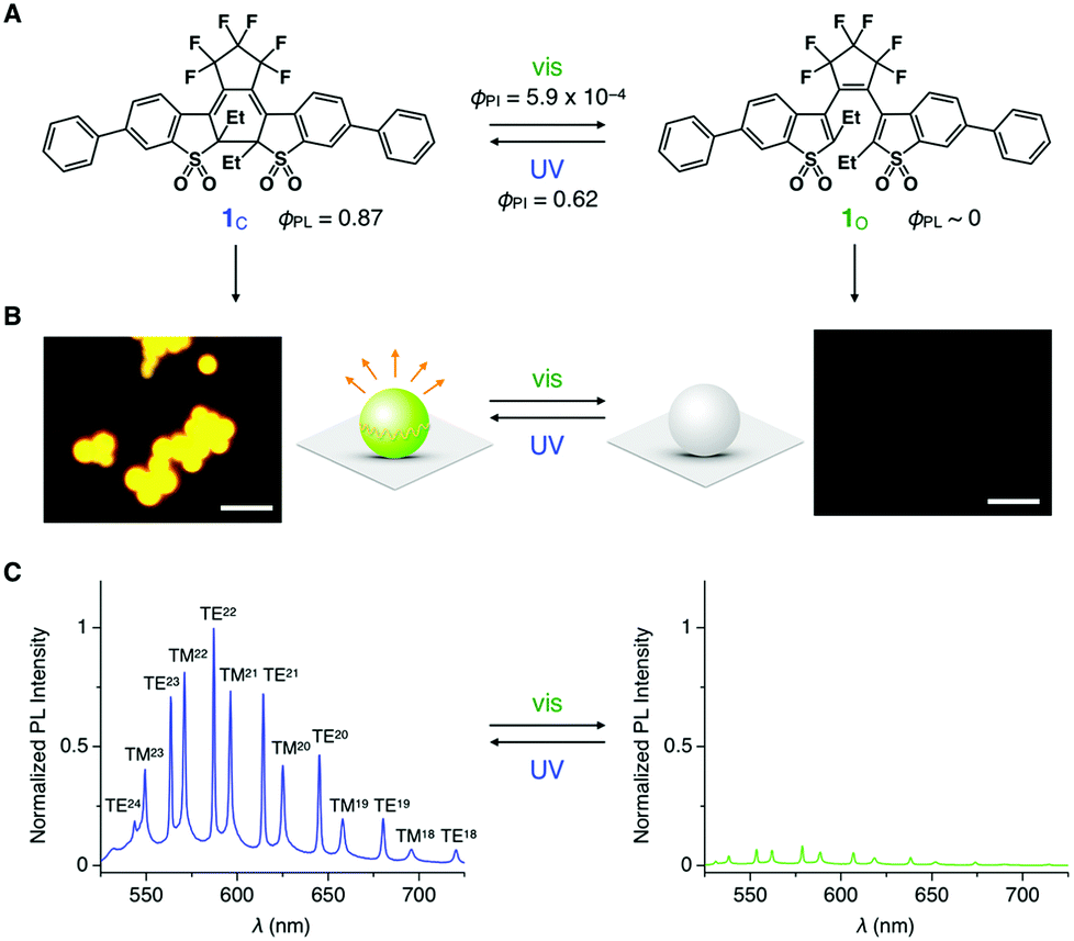 | ||
| Fig. 1 Molecular structure and photoluminescence properties of DAE microspheres. (A) Molecular structures of oxidized diarylethene 1 in closed (1C, left) and open form (1O, right). (B) Fluorescence micrographs and schematic representations of self-assembled microspheres from fluorescent 1C (left) and nonfluorescent 1O (right). λex = 400–440 nm. Scale bars, 10 μm. (C) PL spectra of a single microsphere of 1C (blue) and 1O (green) upon excitation with a focused ps-laser (λex = 470 nm). The WGM indices are denoted above the peak. | ||
Microspheres of 1 were fabricated by an acetone/water interface precipitation method with an initial concentration of 1O in acetone of 1.0 mg mL−1 (for details, see the Experimental section and Fig. S1B, ESI†).26 Slow diffusion of acetone and water at the interface results in precipitation of 1O. Scanning electron microscopy (SEM) of the resultant precipitates shows a microsphere morphology with diameters (d) ranging from 2–8 μm (Fig. S1C and D, ESI†). An X-ray diffraction pattern of the powder sample of the microspheres displays no characteristic diffraction peaks, indicating that the microspheres consist of amorphous aggregation of 1 (Fig. S1E, ESI†). Photoisomerization was definitely observed in the microspheres; almost no fluorescence was observed from the microspheres of 1O (Fig. 1B right). Upon photoirradiation at λex = 350–390 nm of the non-fluorescent microspheres for 1 min, yellow fluorescence appeared from the microspheres, indicating that isomerization takes place from 1O to 1C in the microspheres (Fig. 1B left). The yellow fluorescence gradually disappeared upon photoirradiation at λex = 450–490 nm for 60 min (Fig. 1B and Fig. S1F–H, ESI†).
Upon excitation with a focused laser beam (λex = 470 nm, pulse width (Δ) = 70 ps, see the Experimental section and Fig. S2A, ESI†), a single microsphere of 1C displays clear WGM PL with distinguished transverse electric (TE) and magnetic (TM) modes (Fig. 1C left).31 As d increases, the free spectral range (Δλ) of both the TE and TM modes decreases, and the number of confinement modes increases owing to the increase of the optical path length (Fig. S2B, ESI†). Successive irradiation of the microsphere with a 470 nm laser (1 μW through a 50× objective lens, 120 min) results in photoisomerization from 1C to 1O, leading to the gradual suppression of the PL intensity (Fig. 1C right). Meanwhile, the WGM PL recovers after 90 s of photoirradiation of the microsphere of 1O with UV-LED light (λex = 375 nm, 3.0 W) (Fig. S2C, ESI†).
The photoisomerization of the microspheres is accompanied by shifts of the WGM PL peaks as well as their intensity changes. Irradiation with UV light of a microsphere of 1O is accompanied by a redshift of the WGM peak (Fig. 2A), while irradiation with visible light of a microsphere of 1C results in a blueshift of the WGM peaks (Fig. 2B). The observed shifts are caused by a change in the refractive index (n) upon photoisomerization. The spectroscopic ellipsometry experiments of a cast film of 1 show that the n value decreases from 1.60 to 1.56 upon photoisomerization from 1C to 1O due to breaking of the π-conjugation (Fig. S2D, ESI†). The observed shift of the WGM PL peaks upon photoisomerization corresponds well with the change in n (Fig. 2C and D). From the change in n, the fraction of 1C (f1C) upon photoisomerization is given on the top axis of Fig. 2C and D. According to the refractive index shift, the fraction of 1C upon irradiation with UV-LED light for 90 s was 0.7.
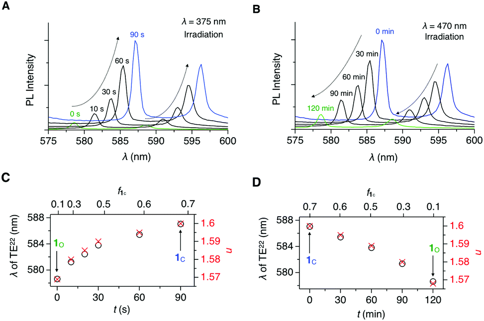 | ||
| Fig. 2 WGM peak shifts upon photoisomerization. (A and B) PL spectra of a single microsphere of 1O in the wavelength range of 575–600 nm, upon 90 s irradiation with a UV-LED at λ = 375 nm (A) and then 120 min irradiation with a laser at λ = 470 nm (B). (C and D) Plots of the peak wavelengths of TE22 and corresponding n simulated by eqn S1 (ESI†) versus the time of photoirradiation with a UV-LED (λex = 375 nm) of the microspheres of 1O (C) and with a ps-pulsed laser (λex = 470 nm) of the microspheres of 1C (D). | ||
Upon two photoisomerization cycles (1O → 1C → 1O → 1C), the PL intensity of the WGM peaks of a microsphere of 1C decreased roughly by half (Fig. S2E and F, ESI†). The photodamage of 1 in the microsphere was possibly caused by long-time irradiation with the focused laser (λ = 470 nm, 150 min) for completing the slow photoisomerization from 1C to 1O. However, the quick writing with long-term preservation of the on-state is beneficial for optical memory applications.
WGM splitting of oblate microspheres
We found that microspheres of 1 are also obtained by slow evaporation of a drop-cast EtOH solution of 1 on a quartz substrate (Fig. 3A top, for details see the Experimental section). The slow evaporation of the solvent results in aggregation of 1 to form well-defined microspheres through a supersaturated state. However, careful observation by SEM indicates that the shape of the spheres is not perfect but oblate to some extent (Fig. 3A bottom, Fig. S3A and B, ESI†). The average ratio of the vertical to the equatorial radius (Rz/Rx) is 0.91 with a standard deviation of 0.057 (Fig. S3C, ESI†). Of interest, upon excitation with a focused ps-laser, the oblate micro-ellipsoid exhibits finely split WGM PL (Fig. 3B). The lowered symmetry from a perfect sphere to an oblate ellipsoid results in the split of the degenerate WGMs, which is well reproduced by an analytical model and numerical simulations with the finite-difference time-domain (FDTD) method (Fig. 3C and Fig. S4, ESI†). Fig. 3D tracks the split of the degenerate transverse WGMs with angular momentum quantum number l = 21 (TE21) as Rz is reduced from 1675 nm to 1415 nm. Degenerate modes with various azimuthal mode numbers (m) are listed in the tabular summary in Fig. 3E and Fig. S4C (ESI†), where the simulated optical near-field distribution of the WGMs agrees well with the spatial distribution of the corresponding spherical harmonics with the same angular momentum quantum number and azimuthal mode number. This analysis confirms that symmetry breaking due to the surface fabrication leads to the fine mode splitting.21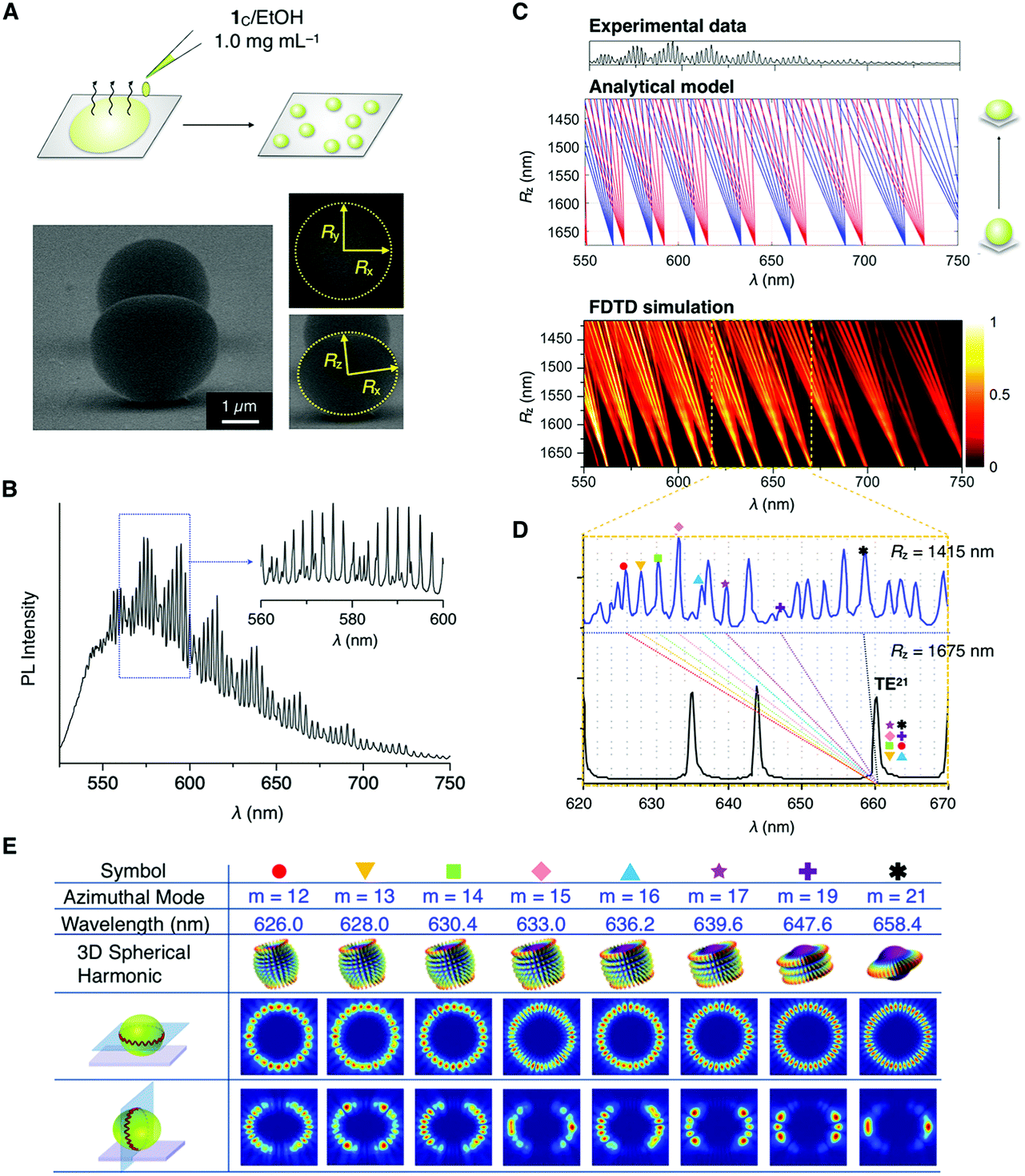 | ||
| Fig. 3 WGM splitting of an oblate micro-ellipsoid of 1. (A) Schematic representation of the drop cast and evaporation procedures for the formation of oblate microspheres and the SEM micrographs of the resultant oblate microspheres. (B) PL spectrum of a single oblate microsphere, with the inset showing the high-resolution PL spectrum obtained with a grating of 1200 grooves mm−1. (C) Experimental PL spectrum in (B) with the continuous fluorescence background removed (top), and the analytically predicted (middle) as well as numerically simulated (bottom) peak positions of splitting WGMs of spheres with various Rz, ranging from 1675 (a perfect sphere) to 1415 nm (an oblate sphere). The blue and red lines in the middle panel indicate TE and TM modes, respectively. (D) Simulated spectra of the perfect sphere (Rz = 1675, black) and the oblate sphere (Rz = 1415, blue), with symbols tracking the splitting of the degenerate WGMs. (E) Tabular summary of the degenerate WGMs showing, from the top to the bottom row, the symbol, azimuthal mode number, peak wavelength, 3D representation of corresponding spherical harmonics, and simulated near-field intensity distribution on a horizontal plane and vertical plane cutting through the centre of the oblate sphere with Rz = 1415 nm. | ||
The average Q-factor (Qav) of the split WGM peaks is 1340 for the oblate ellipsoid with d (= 2Rx) = 2.45 μm. Qav increases as d increases, because a small curvature results in efficient total internal reflection, leading to the reduction of leakage loss. Qav is nearly constant (∼2300) when d is in the range of 3.3–4.5 μm (Fig. S3D red, ESI†).32 This behaviour is in contrast with that of the isotropic microspheres prepared by the interface precipitation method. Qav is ∼400 for isotropic spheres with d = 2–3 μm, and the value increases monotonically as d increases and reaches 1750 for spheres with d = 4.5 μm (Fig. S3D black, ESI†). In the whole d range, Qav of the oblate ellipsoids is greater than that of the isotropic microspheres. The difference is remarkable especially in the small d range (2–3 μm), possibly because originally degenerate WGMs in the isotropic microspheres split from one another by the shape distortion.
Preparation of microarrays by surface self-assembly
By utilizing the surface self-assembly method, highly integrated photoswitchable microdisk arrays are fabricated on a square centimetre area (Fig. 4A). For fabrication, a hydrophobic/hydrophilic micropattern with a 4 μm/2 μm box/line width was prepared on the surface of a quartz substrate by a photolithography technique using parallel vacuum ultraviolet pulsed light (Fig. 4B-i).33 A 20 μL aliquot of an acetone solution of 1 was cast onto the patterned substrate and air-dried. During the evaporation process, 1 tends to form a thin layer at the hydrophobic crossed line area of the surface (Fig. 4B-ii). The substrate was then put into an EtOH vapour atmosphere for 5 h at 25 °C, resulting in the self-organization of 1 to form microdisks at the cross points of the hydrophobic lines (Fig. 4B-iii–v).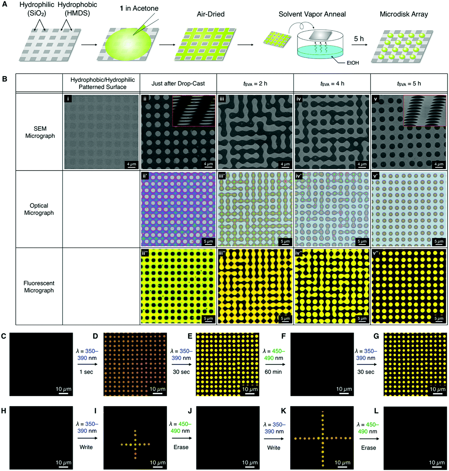 | ||
| Fig. 4 Fabrication process of the microdisk array of 1. (A) Schematic representation of the preparation procedure of the microdisk array of 1 by the drop casting method on a hydrophobic/hydrophilic patterned substrate and subsequent solvent vapour annealing. (B) Tabular summary of the SVA process. (i) SEM micrograph of the hydrophilic/hydrophobic micro-patterned substrate. SEM (ii to v) and optical (ii′ to v′), and fluorescence micrographs (ii′′ to v′′) of a drop-cast film of 1 from acetone solution (1.0 mg mL−1) on the hydrophilic/hydrophobic micro-patterned substrate (ii), which was then put in an EtOH vapour atmosphere for 2 h (iii), 4 h (iv), and 5 h (v). (C–G) Fluorescence micrographs of the microdisk array of 1O (C), which is irradiated with UV light at λ = 350–390 nm for 1 s (D) and further for 30 s (E), then irradiated with visible light at λ = 450–490 nm for 60 min (F), and again irradiated with UV light at λex = 350–390 nm for 30 s (G). λex = 450–490 nm. (H–L) Fluorescence micrographs of the microdisk array of 1O (H), where the microdisks were irradiated one by one with a focused laser at λ = 355 nm to draw a cross pattern (I and K) and irradiated with visible light at λ = 450–490 nm for 60 min to erase the cross pattern (J and L). λex = 450–490 nm. | ||
Fig. S5 (ESI†) shows optical and fluorescence micrographs of the resultant microdisk array with 4 million pixels (∼2000 × 2000) per square centimetre. The average diameter and height of the microdisks are 2 μm and 700 nm, respectively. Changing the concentration of the acetone solution of 1 can control the height of the microdisks from 500 to 800 nm. PL switching of the microdisk array is controllable by shining UV and visible light (Fig. 4C–G). Irradiation with a focused UV laser of selected microdisks of non-fluorescent 1O can draw fluorescence micropatterns, which can further be erased upon irradiation with visible light (Fig. 4H–L).
Array of microresonators with identical WGM fingerprints for unreplicable optical memory
By changing the surface self-assembly process from EtOH vapour annealing to direct immersion into a H2O/acetone mixed solvent (10/6 v/v), the morphology of the film of 1 varied from microdisk arrays to micro-hemisphere arrays (Fig. 5A). Permeation of acetone into a thin film of 1 reorganized it to form a hemispherical structure on the patterned substrate without dissolution of 1. The hemispherical structure formed on the cross points of the hydrophobic lines. The average d and height-to-diameter ratio (h/d) of the resultant hemispheres are 2.68 μm and 0.8, respectively (Fig. S6a, ESI†). Other solvent conditions with low acetone contents hardly form such hemisphere arrays, possibly because of the low solubility of 1 in the mixed solvents (Fig. 5B).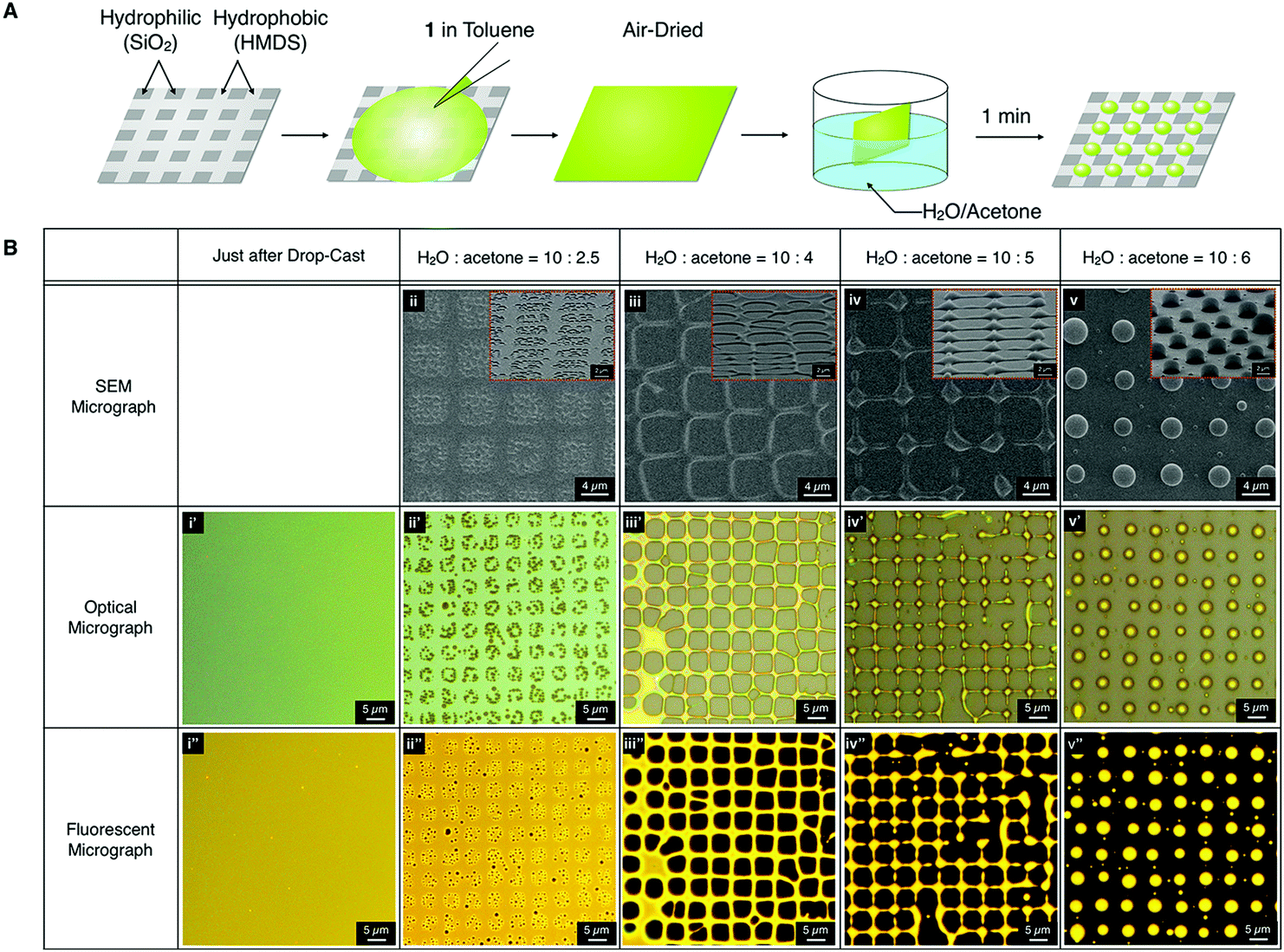 | ||
Fig. 5 Micro-hemisphere array of 1. (A) Schematic representation of the preparation procedure of the micro-hemisphere array of 1 by the drop casting method on a hydrophobic/hydrophilic patterned substrate and subsequent immersion in a H2O/acetone mixed solvent. (B) Tabular summary of the immersion process. SEM (ii–v) and optical (i′–v′), and fluorescence micrographs (i′′–v′′, λex = 450–490 nm) of a drop-cast film of 1 from toluene solution (1.0 mg mL−1) on the hydrophilic/hydrophobic micro-patterned substrate (i) and those immersed into an acetone/H2O mixed solvent for 1 min with a mixing ratio of 10![[thin space (1/6-em)]](https://www.rsc.org/images/entities/char_2009.gif) :2.5 (ii), 10:4 (iii), 10:5 (iv), and 10:6 (v). :2.5 (ii), 10:4 (iii), 10:5 (iv), and 10:6 (v). | ||
By UV irradiation of the micro-hemisphere array through a patterned photomask, a millimeter-scale painting with micrometer resolution can be transferred on a quartz substrate (Fig. 6A and B, and Fig. S6C–E, ESI†). Much more interestingly, the hemisphere generated WGM PL upon focused laser excitation, as the hemispheres possess an equatorial circumference above the substrate. This result is in large contrast with the case of the microdisks, which hardly show WGM PL because of a leakage of confined PL to the substrate (Fig. S5F, ESI†). The hemispheres with d less than 2.5 μm display less clear WGM PL peaks because of the leakage loss of total internal reflection caused by the large curvature (for example, Fig. 6C labels 1–3, 1–5, 2–5 and 3–4). On the other hand, for the hemispheres with d larger than 2.5 μm, a series of sharp WGM PL peaks clearly shows up with Q-factors greater than 200. The percentage of the hemispheres that display high-Q resonator properties (Q > 200) is approximately 67%. The pixel density of a few millions per square centimetre is the highest level of integration for identification tags utilizing optical resonators composed of organic soft materials, considering the minimal hemisphere size that acts as an optical resonator (∼2 μm) and that the pixel distance hardly causes inter-pixel optical interference (several micrometres).
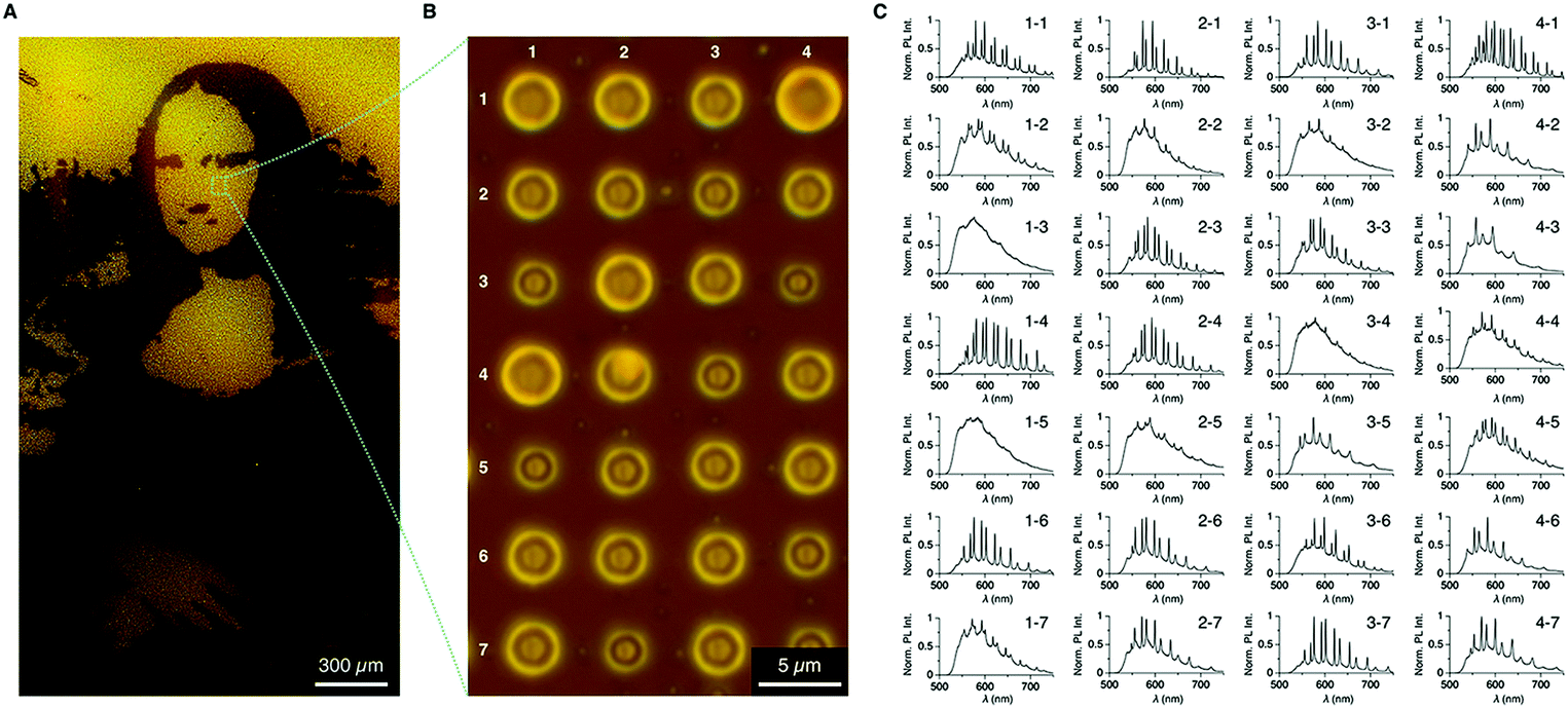 | ||
| Fig. 6 Micro-hemisphere array of 1 with individual WGM fingerprints. (A) Fluorescence micrograph of a micropainting (1.6 × 2.7 mm2) drawn on a quartz substrate, prepared by irradiation at λ = 350–390 nm for 3 min of the microarray of 1O through a patterned photomask. (B) Optical micrograph of the resultant micro-hemisphere array with a 4 × 7 matrix. (C) PL spectra of the arrayed micro-hemispheres. The labels correspond to the matrix in (B). | ||
Because the size and morphology of each hemisphere are not identical, the WGM spectral fingerprints of each hemisphere are different from one another. That is to say, each pixel not only has an on/off PL switching property but also possesses an individual identity as a spectral fingerprint. Such a non-deterministic spectral randomness works as a PUF for identification. In fact, two micropaintings prepared by using a photomask look similar to one another, but the WGM patterns of pixels at the same position display different WGM spectral patterns (Fig. S7, ESI†). This result indicates that reading the WGM patterns can discriminate each micropattern. Furthermore, it should be difficult to replicate the micropatterns including the WGM fingerprints. Therefore, the resultant optical microarrays are proposed for use as an optical authentication system which is highly secured by two-step authentication; the first step by reading out the micropatterns drawn on the substrate utilizing the on/off switching properties of DAE, and the second step by measuring the fluorescence spectral fingerprints of each micro-hemispherical pixel. Although the setup of the two-step optical authentication combining photochromism and optical resonance takes certain work, our system proposes merits of rewritability and higher security authentication in comparison with the reported ones.3–5,34
The present technique for fabricating a large-area microarray is applicable to other fluorescent DAEs such as 2,6-dimethylphenyl-substituted DAE 2 and 2-methylthiophenyl-substituted DAE 3, which display green and red PL colours, respectively, in their closed form (Fig. S8A and B, ESI†).23,28,35,36 Both DAEs form hemispherical arrays on the patterned surface. Each pixel in the microarray displays PL with WGM patterns, similar to that of DAE 1 (Fig. S8C and D, ESI†). The variety of the self-assembled structures of the fluorescent DAEs with a simple fabrication process to form large area arrays is advantageous for practical application of these materials for optical micromemories (Fig. S8E, ESI†).
Conclusions
In conclusion, fluorescence-switchable diarylethenes (DAEs) can self-assemble to form well-defined microspheres in a solution process. The microspheres work as high-Q optical resonators that display whispering gallery mode (WGM) resonant photoluminescence (PL). The WGM PL can be switched on and off by photoisomerization of DAEs upon UV/visible photoirradiation. Self-assembly of DAEs on a substrate surface forms oblate micro-ellipsoids, in which finely split WGMs are observed. The mode splitting by the compressed shape change is unambiguously characterized by numerical simulations. Using hydrophobic/hydrophilic micro-patterned substrates, arrays of microdisks are fabricated, which work as micro-optical memories and paintings. Furthermore, optimization of the assembly conditions can achieve formation of micro-hemisphere arrays. The hemispheres display different WGM patterns from one another, which can be utilized as a highly secure two-step authentication system; the first step by reading out the micropatterns drawn on the substrate, and the second step by measuring the fluorescence spectral fingerprints of each micro-hemispherical pixel. The photochromic microarray with individual WGM fingerprints can be applied for optical authentication devices with a physically unclonable function.Experimental section
Materials and methods
Unless otherwise noted, all reagents and solvents were used as received. Diarylethenes 1, 2, and 3 were synthesized according to a reported procedure.19,29,30 Photoabsorption spectra were recorded on a JASCO V-630 spectrophotometer. Steady-state PL spectra were measured on a JASCO FP-8300 spectrofluorometer. SEM microscopy was performed on a Hitachi model S-3700N SEM operating at 30 kV. Silicon and quartz were used as substrates. For the quartz substrate, a thin layer of Au (<10 nm) was sputtered on the surface to avoid charging. Powder X-ray diffraction (PXRD) patterns were recorded at 25 °C on a RIGAKU model Miniflex600 diffractometer with a CuKα radiation source (40 kV and 15 mA). Optical and fluorescence microscopy observations were carried out using an Olympus model BX53 upright microscope. Ellipsometry measurements were carried out on a J. A. Woollam Japan model M-2000 spectroscopic ellipsometer using a 1–5 μm-thick film of 1.Preparation of microspheres by the interface precipitation method
Microspheres of 1 were prepared by the interface precipitation method (Fig. S1B, ESI†).31 Typically, an acetone solution of 1O ([1O] = 1.0 mg mL−1, 0.2 mL) was carefully added onto a water layer (1 mL). Slow diffusion of the solvents, along with simultaneous evaporation of acetone to air, resulted in the precipitation of microspheres after 6 h of ageing.Preparation of oblate microspheres by surface self-assembly
For the preparation of oblate microspheres of 1, an EtOH solution of 1 (1.0 mg mL−1, 20 μL) was drop cast on a quartz substrate, and the substrate was capped with a Petri dish. The solvent was evaporated at 25 °C in air, and after 2 h, oblate microspheres formed (Fig. 2A top).Fabrication of microdisk and micro-hemisphere arrays of 1–3
For fabrication of hydrophobic/hydrophilic micropatterns, a quartz substrate was immersed in a CHCl3 solution (5 mL) containing 10 μL of 1,1,1,3,3,3-hexamethyldisilazane (HMDS) and allowed to stand overnight. The surface of the resultant HMDS-treated substrate was exposed to parallel vacuum/UV light (150–200 nm wavelength, Ushio Inc., SUS740) through a photomask with a 2 μm (line)/4 μm (box) pattern (Fig. 4A).33 The 4 × 4 μm box pattern of the hydrophilic bare SiO2 surface is darker than the hydrophobic HMDS-treated 2 μm-wide cross line pattern.For fabrication of the microdisk array, 20 μL of an acetone solution of 1 (1.0 mg mL−1) was cast onto the patterned substrate and naturally air-dried (Fig. 4B). During the evaporation process, 1 dewetted and aggregated on the hydrophobic part of the surface of the substrate. The substrate was placed in an EtOH vapour atmosphere and vapour annealed for 5 h at 25 °C, resulting in the assembly of 1 to form microdisk arrays at the cross points of the hydrophobic lines (Fig. 4A and B). The magnified optical and fluorescence microscopy images are shown in Fig. S5 (ESI†).
For fabrication of the micro-hemisphere array, 50 μL of a toluene solution of 1, 2, or 3 (1.0 mg mL−1) was cast onto the patterned substrate and naturally air-dried to form a homogeneous thin film. The substrate was then immersed into a H2O/acetone mixed solvent with a volume ratio of 10/6 for 1 min, resulting in the assembly of micro-hemisphere arrays at the cross point of the hydrophobic lines (Fig. 5A and B). The shape, preparation method and SEM images of the resultant micro-objects are summarized in Fig. S8E (ESI†).
μ-PL measurements by ps-laser pumping
μ-PL measurements of single microspheres with ps-laser pumping were carried out using a μ-PL measurement system (Fig. S2A, ESI†).31 An optical microscope was used with a long-distance 100× objective (NA = 0.8) to identify suitable particles and determine their diameters (d). For the measurements, a WITec μ-PL system was used with a model Alpha 300S microscope combined with a Princeton Instruments model Acton SP2300 monochromator (grating: 300 and 1200 grooves mm−1) and an Andor iDus model DU-401A BR-DD-352 CCD camera cooled to −60 °C. The perimeter of a single microsphere was photoexcited at 25 °C under ambient conditions by a diode pulsed laser (PicoQuant model LDH-D-C-470B with a PDL 828 ‘Sepia II’ driver) with a wavelength (λex), power, integration time, repetition rate (f), pulse duration (λ), and spot size of 470 nm, 1.5 μW, 0.1 s, 2.5 MHz, 70 ps, and ∼0.5 μm, respectively.Author contributions
D. O., J. S. H. and Y. Y. designed the research; D. O., Z. H. L., O. O., X. L., T. M., S. I. and T. N. performed the research; M. M. and M. I. contributed the synthesis; and D. O., J. S. H. and Y. Y. wrote the paper.Conflicts of interest
The authors declare no competing interests.Acknowledgements
This work was partly supported by a Grant-in-Aid for Scientific Research on Innovative Areas “π-System Figuration” (JP17H05141), Scientific Research (A) (JP16H02081), Fund for International Research Collaboration (JP15KK0182), and Young Research Fellowship (JP16J00934) from Japan Society for the Promotion of Science (JSPS), Bilateral Joint Research Program between JSPS and DAAD (BBD30033 and 57402047), New Energy and Industrial Technology Development Organization (NEDO), University of Tsukuba Pre-strategic initiative “Ensemble of light with matters and life”, TIA Kakehashi, Asahi Glass Foundation and Ogasawara Foundation and DFG (CRC 1375 NOA, HU2626/3-1).Notes and references
- R. Maes, Physically unclonable functions, Springer-Verlag, Berlin Heidelberg, 2013 Search PubMed.
- C. Herder, M. D. Yu, F. Koushanfar and S. Devadas, Proc. IEEE, 2014, 102, 1126–1141 Search PubMed.
- R. Pappu, B. Recht, J. Taylor and N. Gershenfeid, Science, 2002, 297, 2026–2030 CrossRef CAS PubMed.
- Y. Liu, F. Han, F. Li, Y. Zhao, M. Chen, Z. Xu, X. Zheng, H. Hu, J. Yao, T. Guo, W. Lin, Y. Zheng, B. You, P. Liu, Y. Li and L. Qian, Nat. Commun., 2019, 10, 2409 CrossRef PubMed.
- Z. Hu, M. J. Miguel, L. Comeras, H. Park, J. Tang, A. Afzali, G. S. Tulevski, J. B. Hannon, M. Liehr and S. J. Han, Nat. Nanotechnol., 2016, 11, 559–565 CrossRef CAS PubMed.
- B. Yoon, J. Lee, I. S. Park, S. Jeon, J. Lee and J. M. Kim, J. Mater. Chem. C, 2013, 1, 2388–2403 RSC.
- H. Sun, S. Liu, W. Lin, K. Y. Zhang, W. Lv, X. Huang, F. Huo, H. Yang, G. Jenkins, Q. Zhao and W. Huang, Nat. Commun., 2014, 5, 3601 CrossRef PubMed.
- Y. Sagara, S. Yamane, M. Mitani, C. Weder and T. Kato, Adv. Mater., 2015, 28, 1073–1095 CrossRef PubMed.
- P. Kumar, S. Singh and B. K. Gupta, Nanoscale, 2016, 8, 14297–14340 RSC.
- C. Zhang, B. Wang, W. Li, S. Huang, L. Kong, Z. Li and L. Li, Nat. Commun., 2017, 8, 1138 CrossRef PubMed.
- Z. Gao, Y. Han and F. Wang, Nat. Commun., 2018, 9, 3977 CrossRef PubMed.
- K. Jiang, L. Zhang, J. Lu, C. Xu, C. Cai and H. Lin, Angew. Chem., Int. Ed., 2016, 55, 7231–7235 CrossRef CAS PubMed.
- W. Tian, J. Zhang, J. Yu, J. Wu, J. Zhang, J. He and F. Wang, Adv. Funct. Mater., 2017, 1703548 Search PubMed.
- J. Li, H. K. Bisoyi, S. Lin, J. Guo and Q. Li, Angew. Chem., Int. Ed., 2019, 131, 16198–16202 CrossRef.
- J. Li, H. K. Bisoyi, J. Tian, J. Guo and Q. Li, Adv. Mater., 2019, 1807751 CrossRef PubMed.
- K. J. Vahala, Nature, 2003, 424, 839–846 CrossRef CAS PubMed.
- S. Yang, Y. Wang and H. Sun, Adv. Opt. Mater., 2015, 3, 1136–1162 CrossRef CAS.
- D. Venkatakrishnarao, E. A. Mamonov, T. V. Murzina and R. Chandrasekar, Adv. Opt. Mater., 2018, 6, 1800343 CrossRef.
- M. Schubert, A. Steude, P. Liehm, N. M. Kronenberg, M. Karl, E. C. Campbell, S. J. Powis and M. C. Gather, Nano Lett., 2015, 15, 5647–5652 CrossRef CAS PubMed.
- Z. Gao, C. Wei, Y. Yan, W. Zhang, H. Dong, J. Zhao, J. Yi, C. Zhang, Y. J. Li and Y. S. Zhao, Adv. Mater., 2017, 29, 1701558 CrossRef PubMed.
- D. Braam, S. Kushida, R. Niemöller, G. Prinz, H. Saito, T. Kanbara, J. Kuwabara, Y. Yamamoto and A. Lorke, Sci. Rep., 2016, 6, 19635 CrossRef CAS PubMed.
- M. M. Russew and S. Hecht, Adv. Mater., 2010, 22, 3348–3360 CrossRef CAS PubMed.
- K. Uno, H. Niikura, M. Morimoto, Y. Ishibashi, H. Miyasaka and M. Irie, J. Am. Chem. Soc., 2011, 133, 13558–13564 CrossRef CAS PubMed.
- R. Kashihara, M. Morimoto, S. Ito, H. Miyasaka and M. Irie, J. Am. Chem. Soc., 2017, 139, 16498–16501 CrossRef CAS PubMed.
- M. Irie, T. Fukaminato, K. Matsuda and S. Kobatake, Chem. Rev., 2014, 114, 12174–12277 CrossRef CAS PubMed.
- O. Nevskyi, D. Sysoiev, A. Oppermann, T. Huhn and D. Wöll, Angew. Chem., Int. Ed., 2016, 128, 12890–12894 CrossRef.
- D. Kim, J. E. Kwon and S. Y. Park, Adv. Funct. Mater., 2017, 28, 1706213 CrossRef.
- M. Irie and M. Morimoto, Bull. Chem. Soc. Jpn., 2018, 91, 237–250 CrossRef CAS.
- C. W. Hsu, C. Sauvée, H. Sundén and J. Andréasson, Chem. Sci., 2018, 114, 12174–12178 Search PubMed.
- M. Yu, P. Zhang, B. P. Krishnan, H. Wang, Y. Gao, S. Chen, R. Zeng, J. Cui and J. Chen, Adv. Funct. Mater., 2018, 1804759 CrossRef.
- D. Okada, T. Nakamura, D. Braam, T. D. Dao, S. Ishii, T. Nagao, A. Lorke, T. Nabeshima and Y. Yamamoto, ACS Nano, 2016, 10, 7058–7063 CrossRef CAS PubMed.
- M. L. Gorodetsky, A. A. Savchenkov and V. S. Ilchenko, Opt. Lett., 1996, 21, 1–3 CrossRef PubMed.
- X. Liu, M. Kanehara, C. Liu, K. Sakamoto, T. Yasuda, J. Takeya and T. Minari, Adv. Mater., 2016, 28, 6568–6573 CrossRef CAS PubMed.
- B. C. Grubel, B. T. Bosworth, M. R. Kossey, H. Sun, A. B. Cooper, M. A. Foster and A. C. Foster, Opt. Express, 2017, 25, 12710–12721 CrossRef CAS PubMed.
- Y. Takagi, M. Morimoto, R. Kashihara, S. Fujinami, S. Ito, H. Miyasaka and M. Irie, Tetrahedron, 2017, 73, 4918–4924 CrossRef CAS.
- M. Morimoto, R. Kashihara, K. Mutoh, Y. Kobayashi, J. Abe, H. Sotome, S. Ito, H. Miyasaka and M. Irie, CrystEngComm, 2016, 18, 7241–7248 RSC.
Footnote |
| † Electronic supplementary information (ESI) available. See DOI: 10.1039/d0mh00566e |
| This journal is © The Royal Society of Chemistry 2020 |