Platinum single atoms on tin oxide ultrathin films for extremely sensitive gas detection

Yongshan Xu a, Wei Zheng a, Xianghong Liu *ab, Liqiang Zhang c, Lingli Zheng a, Chen Yang a, Nicola Pinna d and Jun Zhang *ab
aCollege of Physics, Center for Marine Observation and Communications, Qingdao University, Qingdao 266071, China. E-mail: xianghong.liu@qdu.edu.cn; jun@qdu.edu.cn
bKey Laboratory of Advanced Energy Materials Chemistry (Ministry of Education), Nankai University, Tianjin 300071, China
cClean Nano Energy Center, State Key Laboratory of Metastable Materials Science and Technology, Yanshan University, Qinhuangdao 066004, China
dInstitut für Chemie and IRIS Adlershof, Humboldt-Universität zu Berlin, Brook-Taylor-Str. 2, 12489 Berlin, Germany

Received 23rd March 2020 , Accepted 16th April 2020

First published on 16th April 2020


Abstract

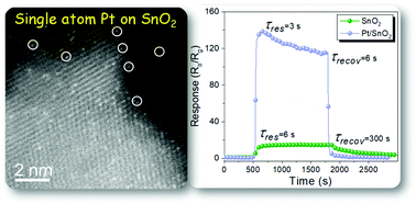
Single atom Pt functionalized SnO2 ultrathin films are synthesized by atomic layer deposition (ALD) for application as sensing layers in resistive gas sensors. Here it is shown that the electronic conductivity of the SnO2 ultrathin films is very sensitive to the exposure to triethylamine (TEA), and that the thickness of the SnO2 films (from 4 to 18 nm) has a crucial effect on the sensor response. The 9 nm thick SnO2 film shows the best response to TEA, while a further decrease in the film thickness, i.e., 4 nm, leads to a very weak response due to the two orders of magnitude lower carrier concentration. Single atom Pt catalysts deposited on the 9 nm SnO2 film result in an unexpectedly high enhancement in the sensor response and also a decrease of the sensor working temperature. Consequently, Pt/SnO2 thin film sensors show the highest response of 136.2 to 10 ppm TEA at an optimal temperature of 200 °C (that of a pristine SnO2 film sensor is 260 °C), which is improved by a factor of 9 compared to that of pristine SnO2. Moreover, the Pt/SnO2 sensor exhibits an ultrahigh sensitivity of 8.76 ppm−1 and an extremely low limit of detection (LOD) of 7 ppb, which to our best knowledge are far superior to any previous report. Very fast response and recovery times (3/6 s) are also recorded, thus making our sensor platform highly suitable for highly-demanding applications. Mechanistic investigations reveal that the outstanding sensing performances originate from the synergistic combination of the optimized film thickness comparable to the Debye length of SnO2 and the spillover activation of oxygen by single atom Pt catalysts, as well as the oxygen vacancies in the SnO2 films.


New Concepts

Herein, we report the conceptual demonstration of single atom Pt functionalized SnO2 ultrathin films by atomic layer deposition (ALD) and their utilization as sensing layers for gas sensors achieving record sensitivity towards detection of VOCs. This work differs from existing research in both fundamental mechanistic research and technological potential in developing sensing materials for advanced sensors. Platinum single atoms are, for the first time, employed to improve the sensing properties of SnO2 film sensors, enabling an exceptionally high sensitivity of 8.76 ppm−1 and an extremely low detection limit of 7 ppb, as well as very fast response and recovery, which to our best knowledge are far superior to those previously reported. Our mechanistic investigations reveal that the outstanding sensing performances originate from the spillover activation of oxygen by the single atom Pt catalyst, which has been a critical question in the area of gas sensing materials. Furthermore, the optimized film thickness comparable to the Debye length of SnO2 and the oxygen vacancies in the SnO2 films also play a role in the sensor response. In a broader context, this work presents a breakthrough in the fundamental research of single atom Pt catalysts and SnO2 ultrathin films in application to gas sensors, which has paramount significance in future sensor networks and the Internet of things.

1. Introduction

The fast development of the Internet of things (IoT) requires miniaturized and low power consumption gas sensors that are capable of rapidly detecting trace gases, allowing building vast and smart sensor networks.1 Gas sensors are widely used to monitor gas leakage and air pollution and for household security, as well as in some emerging areas such as exhaled breath diagnosis for the sake of the safety and health of people.2–6 During the past few decades, nanostructured materials including nanowires, nanosheets and 3D architectures have demonstrated great superiority as sensing layers in chemiresistive sensor devices to achieve high sensitivity to particular target molecules.7–11 Various nanostructures produced by solution processes such as solvothermal or hydrothermal methods generally appear as powdery materials. These materials are usually made into sensing layers by using methods like screen-printing, dip-coating and drop-coating to fabricate thick film sensor devices, e.g. the Figaro sensor using ceramic tube or plate electrodes. This established fabrication process is quite effective and low-cost; however, it suffers from a lack of control in terms of the uniformity of the sensing layer. High-precision sensing layer technology is of great significance for the reliable production of sensors and sensor arrays for emerging applications such as sensor integration, pattern recognition, and sensor networks. In this regard, thin film technology is highly advantageous due to its capability of growing films with high uniformity over a large area, delicate control over film thickness, and high compatibility with current micro/nano-fabrication technologies, such as micro-electro-mechanical system (MEMS) gas sensors for the future IoT.

SnO2 has been one of the most successful semiconductor materials for thick film gas sensors ever since its integration in a commercial device,12 due to its high sensitivity, good stability and low cost. The sensing mechanism of SnO2 gas sensors is based on the modulation of the electron depletion layer (EDL) by reactions between target molecules and adsorbed oxygen species. During the past few decades, SnO2 thin film-based gas sensors have been shown to respond to molecules including CO, H2, H2S, NO2, CH4 and volatile organic compounds (VOCs).13–18 SnO2 thin films fabricated by pulse laser deposition,14 spray pyrolysis,16 atomic layer deposition (ALD)17 and sputtering19 generally have thicknesses ranging from dozens to hundreds of nm. We previously reported the coating of carbon nanotubes (CNTs) with 3 nm thick SnO2 for detection of NO2 by ALD;20 however, pristine large-area ultrathin SnO2 films with thicknesses below 10 nm,15,21 as well as their potential in batch fabrication of gas sensors, have rarely been reported. In addition, ultrathin films are an ideal platform to study the surface functionalization of noble metal catalysts and their catalytic effects, as well as structural effects such as film thickness on their sensing properties and mechanisms, which is of vital importance to develop thin film gas sensors.

To improve the “4S” functions of sensors, i.e., selectivity, sensitivity, speed and stability, noble metals such as platinum (Pt) nanoparticles have been widely used as catalysts loaded onto the surfaces of metal oxides. Recently, single atom catalysts have attracted significant attention world-wide in diverse areas. Compared to conventional nanoparticle catalysts, single atom catalysts can create many atomically active sites on host materials with very high utilization efficiency of the noble metals, and exhibit optimized surface electronic properties and enhanced catalytic activity.22,23 Pt single atom catalysts can be readily prepared by low-cost liquid-phase reactions.24,25 However, such protocols are not applicable to semiconductor thin films because thin film sensing layers are commonly grown on a rigid, e.g. silicon, substrate. In principle, vapor phase methods such as atomic layer deposition (ALD), based on self-limiting surface reactions,26,27 can provide an efficient way to functionalize thin film surfaces with single atom catalysts.28,29

In this work, we report the fabrication of thin film gas sensors based on highly uniform SnO2 films by ALD with ultrathin thicknesses in the range of 4–18 nm. The thickness-dependent response on exposure to triethylamine (TEA) has been studied. In contrast to the well-known grain size effect,30 the SnO2 thin film with a moderate thickness of 9 nm delivers the best response. Pt single atom catalysts have been deposited onto SnO2 thin films by ALD to further improve the sensor sensitivity and detection limit, allowing for a superior limit of detection (LOD) of 7 ppb at 200 °C, which is far beyond the threshold limit value (1 ppm) of TEA established by the American Conference of Governmental Industrial Hygienists.31 Such ultrasensitive sensors based on single atom Pt/SnO2 thin films, to the best of our knowledge, have not been reported before. More appealing, the entire fabrication process based on ALD is perfectly compatible with the current micro/nanofabrication technology, successfully overcoming the poor homogeneity of sensing layers fabricated by conventional methods, and can lead to the development of high performance and reliable gas sensor devices.

2. Results and discussion

SnO2 thin films were deposited on SiO2/Si wafers by thermal ALD using tetrakis(dimethylamino)tin(IV) (TDMASn) and H2O as the precursors (details are provided in the ESI). The surface chemistry can be ascribed to the following half-reactions (1) and (2) and overall reaction (3):32
 
(OH)x* + Sn(DMA)4 → (O)xSn(DMA)4−x* + xHDMA↑(1)
 
(OH)xSn(DMA)4−x* + 2H2O → (OH)x* + SnO2 + (4 − x)HDMA↑(2)
 
Sn(DMA)4 + 2H2O → SnO2 + 4HDMA↑(3)
where “*” represents the surface-bound species, DMA is the dimethylamino ligand, HDMA is the gas phase of dimethylamino, and x is the number of DMA ligands released during the TDMASn pulse.

The thicknesses of the thin films were adjusted in the 4–18 nm range by changing the number of ALD cycles. The surface of the SnO2 thin film with a thickness of 9 nm was observed by scanning electron microscopy (SEM) and optical microscopy. As shown in Fig. 1a and Fig. S1b (ESI), a thin and conformal film was deposited. At higher magnification (Fig. 1b) it becomes clear that the thin film is composed of uniform crystallites. Such a thin film with a high uniformity, when serving as the sensing layer, can ensure minimum differences between different sensor devices from batch production (Fig. S1c, ESI). The formation of a high-quality thin film is due to the self-terminated surface reaction of ALD, the appropriate doses of the precursors, the growth temperature and pressure, and the low roughness of the substrate used. As a comparison, the surface structures of the sensing layers of commercial TGS 2602 gas sensors (thick-film technique), which are mainly used for VOC detection in air, are shown in Fig. S3 (ESI). It is seen that the sensing layers of the three devices exhibit quite inhomogeneous surfaces, along with some cracks present in the sensing layers. This may result in an unsatisfactory reproducibility of the commercial sensors. Actually gas sensing tests confirmed that the three commercial devices deliver quite different sensing responses to triethylamine (Fig. S4a and b, ESI) at an optimal operating temperature of 260 °C. On the other hand, our sensor based on the SnO2 thin film with a thickness of 9 nm deposited by ALD shows a higher response and better stability and repeatability compared to the commercial TGS 2602 gas sensors under otherwise the same conditions (Fig. S4c and d, ESI).


image file: d0mh00495b-f1.tif
Fig. 1 The structural characterization of Pt/SnO2 and SnO2 thin films: (a and b) SEM images of a SnO2 thin film, (c) HAADF-STEM image and (d) EDS-STEM elemental mapping of single atom Pt/SnO2 thin films, and AFM characterization of (e) SnO2 and (f) Pt/SnO2 thin films.

Pt single atom catalysts were grown on the SnO2 thin film with a thickness of 9 nm by a thermal ALD process with trimethyl(methylcyclopentadienyl)platinum(IV) (MeCpPtMe3) (99%) and O3 as the precursors (details can be seen in the ESI). High angle annular dark field scanning transmission electron microscopy (HAADF-STEM) was used to characterize the Pt single atom catalysts grown on the SnO2 thin film. Pt single atoms, exhibiting a brighter contrast, are uniformly dispersed onto the SnO2 substrate (Fig. 1c). The lattice fringes with spacing values of 0.26 and 0.33 nm are ascribed to the (101) and (110) planes of SnO2 and attributed to the substrate. The STEM-energy dispersive X-ray spectroscopy (EDS) maps in Fig. 1d reveal a homogeneous dispersion of Sn, O and Pt. X-ray Photoelectron Spectroscopy (XPS) was carried out to characterize the surface chemistry of the thin films. The XPS spectra of Sn 3d in Fig. S2 (ESI) indicate that the thin film after calcination at 500 °C has a fully oxidized state, i.e. Sn(IV) with binding energies of 494.67 (3d3/2) eV and 486.22 (3d5/2) eV, corresponding to SnO2. The binding energies of the as-grown thin film by ALD suggest a mixed valence state of Sn(II) and Sn(IV). The distinguished deviation in binding energy indicates a different electronic environment of the Sn ions, which may be due to the large concentration of oxygen vacancies in the as-deposited SnO2 thin film. The surface morphologies of the thin films with and without Pt were studied by Atomic Force Microscopy (AFM). As shown in Fig. 1e and f, the Pt/SnO2 thin film has a surface root mean square (RMS) roughness of 420 pm, which is comparable to that (470 pm) of a pristine SnO2 thin film, revealing that the Pt/SnO2 and SnO2 thin films have similar surface features. Apparently, the SnO2 thin films deposited by ALD possess high quality with very high surface homogeneity over a large area, which provides a large opportunity to function as the sensing layers for scalable manufacture of gas sensors (Fig. S1c, ESI).

The impact of the SnO2 thin film thickness on the sensor response was first studied by exposing the SnO2 thin film sensors to 10, 50 and 100 ppm triethylamine (TEA) at 200 °C. As shown in Fig. 2a–c, except for the sensor based on a 4 nm thick SnO2 thin film, the other sensors based on 9, 13, and 18 nm thick SnO2 thin films exhibit fast response and recovery dynamics. At all the measured TEA concentrations, the SnO2 thin film with a thickness of 9 nm exhibits the highest response (cf.Fig. 2d) and the 4 nm thick film shows negligible response. This result has been beyond our expectation. To answer why the sensor based on the 4 nm thick SnO2 thin film is not sensitive, we studied the surface microstructure and the electrical properties of the thin films. First, we characterized the RMS roughness of these films by AFM. A thin film with a much larger surface roughness might have a larger surface area to absorb more surface oxygen species (Fig. S5, ESI), and thus might show a higher response. As displayed in Fig. 3, the AFM results reveal that these thin films have comparable RMS roughnesses in the range of 366–538 pm, which are also comparable to our previous report.20 This result indicates that the surface roughnesses of these films do not exhibit much differences. Therefore, we can conclude that the highly different sensor responses in Fig. 2d are not attributable to the surface roughnesses of the thin films.


image file: d0mh00495b-f2.tif
Fig. 2 Dynamic transients of SnO2 thin films with different thicknesses (4, 9, 13, and 18 nm) on exposure to different concentrations of triethylamine at a temperature of 200 °C: (a) 10 ppm, (b) 50 ppm and (c) 100 ppm, and (d) comparison of the sensor responses.

image file: d0mh00495b-f3.tif
Fig. 3 3D surface structures tested by AFM of (a) a SiO2/Si wafer and SnO2 thin films with different thicknesses of (b) 4 nm, (c) 9 nm, (d) 13 nm, and (e) 18 nm, and (f) the surface roughnesses of the thin films obtained for different ALD cycles.

Moreover, we conducted Hall experiments to measure the electrical properties of the thin films. It turned out that the 4 nm thick film has a rather low carrier concentration (2.17 × 1014 cm−3), which is two orders of magnitude lower than that (9.22 × 1016 cm−3) of the 9 nm thick film. Considering that the sensor resistances based on the 4 nm (3.4 MΩ) and 9 nm (2.2 MΩ) thick films are not highly different, the low response of the 4 nm thick film in Fig. 2d can be ascribed to its very low carrier concentration. Based on the tested carrier concentration, the Debye length (LD) of the SnO2 thin film is calculated to be 14.5 nm (detailed calculation is provided in the ESI). Compared to a SnO2 thick film with a LD of 3.6 nm,33 our thin film has a much larger LD value (14.5 nm), which is due to the lower carrier concentration compared with that (2.14 × 1018 cm−3) of the thick film. Therefore, our SnO2 ALD thin films with thicknesses below 14.5 nm can be completely depleted of electrons due to the EDL built by surface adsorbed oxygen species, which will result in the largest variation in film resistance when exposed to an analyte, and hence in an improved sensor response.20,30 On the other hand, the modulation of the resistance is very small for the 4 nm thick film due to its significantly lower carrier concentration. A smaller change in the resistance is also expected for the 18 nm thick film, because its thickness is larger than the calculated Debye length, leading to only a partial electron depletion of the crystallites when exposed to oxygen.

Pt has been extensively employed to improve the sensor properties of various semiconductor metal oxides due to its catalytic activity, i.e. spillover effect. However, to the best of our knowledge, there has been no report involving Pt single atom catalysts on SnO2 for gas sensor applications. Fig. 4a demonstrates the effect of Pt single atom catalysts on the sensor response at various working temperatures. The sensor based on Pt/SnO2 has a lower optimal working temperature of 200 °C compared to pristine SnO2 (260 °C). The response of Pt/SnO2 to 10 ppm TEA is as high as 136.2, which is almost 7 times higher than that (20.3) of SnO2. The dynamic response–recovery curves on exposure to 10 ppm TEA are compared in Fig. 4b, showing that the Pt/SnO2 sensor has much faster response and recovery times. The response time is 3 s, only half of that of SnO2. However, the most pronounced improvement can be seen in the recovery process. The Pt/SnO2 sensor can recover within 6 s, which is two orders of magnitude faster than pure SnO2 (300 s). The very fast response–recovery dynamics of the Pt/SnO2 sensor can be attributed to the Pt single atoms, which can reduce the activation energy of surface reactions and enhance the adsorption of TEA in response and the desorption of the resultant molecules in the recovery process.34 The gas sensing characteristics of the thin films were further evaluated by exposure to various TEA concentrations (0.1–100 ppm). In Fig. 4c and d, it is observed that the sensor responses increase with increasing gas concentration. The Pt/SnO2 sensor always displays significantly higher responses compared to SnO2, together with very fast response and recovery. Fig. 4e exhibits the linear fitting of the sensor response as a function of the TEA concentration, indicating that the Pt/SnO2 sensor has a much higher sensitivity of 8.76 ppm−1 than SnO2 (2.23 ppm−1). The limit of detection can be calculated from eqn (4):35

 
LOD = 3σ/s(4)
where σ is the standard deviation of the response and s is the slope of the calibration curve. The limits of detection of both sensors are calculated to be 7 and 98 ppb, respectively. In order to characterize the sensor selectivity, the thin film sensors were further exposed to a group of molecules including C6H15N, C2H6O, CH3COCH3, CH3(CH2)3OH, CH3OH, HCHO and C7H8. As shown in Fig. 4f, the Pt/SnO2 sensor shows improved responses to all the gases. The selectivity coefficients in Fig. 4g calculated using the responses to the various analytes indicate that single atom Pt catalysts dramatically improve the selectivity toward TEA.


image file: d0mh00495b-f4.tif
Fig. 4 (a) Responses to 10 ppm TEA of SnO2 and Pt/SnO2 thin films (9 nm) at different temperatures; (b) dynamic transients of SnO2 and Pt/SnO2 thin films to 10 ppm TEA at 200 °C, and dynamic transients of (c) Pt/SnO2 and (d) SnO2 thin films to TEA concentrations in the range of 0.1–100 ppm at 200 °C; (e) linear fitting responses of SnO2 and Pt/SnO2 thin films; and (f) selectivity and (g) selectivity coefficients of SnO2 and Pt/SnO2 thin films sensors to various 10 ppm gases toward TEA.

It has been suggested that noble metal catalysts for gas sensors participate in an electronic or a chemical sensitization, which is highly dependent on the oxidation state of the metals.36 The former is due to the equilibrium of the Fermi levels of the oxidized metal and the semiconductor, which modulates the carrier concentration of the semiconductor sensing layers. The latter is ascribed to the spillover effects of the noble metal catalyst, which promotes the dissociation of molecular oxygen into more active surface atomic oxygen species. The core level XPS spectra of Pt 4f were collected from the Pt/SnO2 thin films annealed at 500 °C in Ar/H2. As shown in Fig. 5a, the signal of Pt shows two deconvoluted peaks at binding energies of 73.95 eV for Pt 4f5/2 and 70.67 eV for Pt 4f7/2 with a difference of 3.28 eV, which can be assigned to metallic Pt.37,38 For comparison, the Pt/SnO2 thin film was also annealed in air under the same conditions. It can be observed in Fig. 5a that the signal of Pt is highly distinct from that of metallic Pt in Pt/SnO2. The doublet is present at 75.38 eV for Pt 4f5/2 and 72.08 eV for Pt 4f7/2 with a difference of 3.30 eV, indicating an oxidation state of Pt(II) as in PtO.38,39 The XPS spectrum of the as-deposited Pt/SnO2 thin films after ALD without any thermal process in Fig. 5a reveals a doublet at 74.92 eV for Pt 4f5/2 and 71.62 eV for Pt 4f7/2 that are inconsistent with neither Pt(II) nor Pt(0), which can be depicted as PtOx (x < 1). The presence of PtOx after Pt ALD is probably due to the partial oxidation of Pt by O3 serving as a counter reactant.37 After annealing in Ar/H2, the PtOx is reduced to metallic Pt.


image file: d0mh00495b-f5.tif
Fig. 5 (a) The core level XPS spectra of Pt 4f in Pt/SnO2 thin films after annealing in Ar/H2 at 500 °C, PtO/SnO2 after annealing in air at 500 °C and the as-deposited PtOx/SnO2 without annealing, and (b) XPS spectra of O 1s in Pt/SnO2, PtO/SnO2 and pristine SnO2 thin films.

Based on the above discussion on the oxidation states of Pt, it is very interesting to figure out which kind of sensitization, i.e., electronic by PtO or chemical by Pt, is more effective in improving the sensor performance. Note that this question has seldom been addressed in the literature.40 Fig. S7 (ESI) displays the dynamic response–recovery curves of Pt/SnO2 and PtO/SnO2 thin films on detection of 5 ppm TEA. The Pt/SnO2 sensor has a response of 80.1, which is four times higher than that (17.2) of PtO/SnO2. This result indicates that the significantly different sensor responses are related to the different oxidation states of the Pt catalyst. By comparing the Sn 3d core-level spectra of Pt/SnO2 and SnO2 shown in Fig. S2 (ESI), it is found that the peak positions of the two samples show no significant shift, indicating a weak electronic interaction between Pt and SnO2. Thus, the promotion effect of Pt catalysts is generally ascribed to the spillover effect,40i.e., the dissociation of molecular oxygen into negatively charged oxygen species with high reactivity. To prove the activation of oxygen by Pt, the XPS spectra of O 1s of the Pt/SnO2, PtO/SnO2 and SnO2 thin films are shown in Fig. 5b. It is seen that the spectra exhibit dramatic differences. The O 1s spectra of Pt/SnO2 are deconvoluted into three O components, i.e., lattice oxygen (Olatt), surface adsorbed oxygen (Oads) and surface OH groups or molecular water (OOH). The surface adsorbed negatively charged oxygen species (O2, O, O2−), i.e. Oads, are highly oxidative and are responsible for the sensing reactions. The XPS results reveal that the Pt/SnO2 film has a very high surface concentration (64.4%) of Oads, which is higher than that of PtO/SnO2 (52.8%) and pristine SnO2 (16.5%). The enhanced concentration of Oads can be attributed to the catalytic spillover effect of Pt atoms that substantially activate the molecular oxygen, thereby promoting the sensing reactions to produce a larger change in the sensor resistance to give a much higher response. Although the PtO/SnO2 film has a high concentration of Oads (52.8%), the sensor response is inferior to that of Pt/SnO2, as shown in Fig. S7 (ESI). In addition, electrical tests reveal that the Pt/SnO2 sensor has a much higher resistance (30.1 MΩ) than PtO/SnO2 (1.1 MΩ), which can be attributed to the improved adsorption of oxygen species that would take electrons from the conduction band of SnO2 to form a pronounced EDL, thus decreasing the sensor conductivity.

The presence of oxygen vacancies in MOS has been suggested to improve the gas sensor responses.41 SnO2 is an n-type semiconductor due to its intrinsic oxygen under-stoichiometry. The removal of O2− from the SnO2 lattice generates oxygen vacancies, which can serve as donors to trap electrons from the conduction band of SnO2, thus leading to the formation of paramagnetic centers that can be identified by electron paramagnetic resonance (EPR) spectroscopy.42 To further elucidate the sensing mechanism, EPR studies were carried out to investigate the presence of oxygen vacancies in the thin films. As shown in Fig. S6 (ESI), the EPR spectra show obvious isotropic signals at a g factor of 2.003, which clearly manifest the presence of oxygen vacancies in the thin films studied. They also reveal that the oxygen vacancies in the films are identical paramagnetic centers, i.e. singly ionized oxygen vacancies. In addition, the higher intensity of the EPR signal in Pt/SnO2 also suggests a higher concentration of oxygen vacancies than those of PtO/SnO2 and SnO2, which is believed to have resulted from the annealing process in Ar/H2. To clarify the role of the oxygen vacancies in our SnO2 thin films, a sensor based on SnO2 thin films annealed in Ar/H2 was also tested. The dynamic transients to TEA concentrations in the range of 0.1–100 ppm at 200 °C are shown in Fig. S8 (ESI). Compared to the sensing performance (Fig. 4d) of SnO2 thin films annealed in air, the response of SnO2 annealed in Ar/H2 is seen to be slightly improved. This result indicates that oxygen vacancies have a limited effect on the sensing response of our films. Hence, our experiments lead to the conclusion that single Pt(0) atoms play the most important role in the improvement of the sensor response.

Based on these experiments, a plausible sensing mechanism is schematically proposed in Fig. 6. When the SnO2 thin film is exposed to air, O2 molecules will adsorb on the surface of the SnO2 thin film and extract free electrons from the conduction band of SnO2 to form adsorbed oxygen negative species Ox (i.e. O2, O and O2−) to fill the oxygen vacancies; this process leads to the generation of an EDL on the surface of the SnO2 thin film, which in turn increases the resistance and reduces the conductivity of SnO2.43 Moreover, an appropriate thin film thickness (9 nm) can result in a complete electron depletion of the thin film material. When the SnO2 film is exposed to TEA, the oxidizing adsorbed oxygen Ox reacts with the reducing TEA molecules to form NO2, CO2 and H2O, and release electrons back to the conduction band of the SnO2 film.44 As a result, the surface EDL of SnO2 becomes thinner and the potential barrier is reduced (Fig. 6c); thus the recorded conductivity of the film increases.


image file: d0mh00495b-f6.tif
Fig. 6 Surface reaction mechanisms of Pt/SnO2 thin films in (a) air and (b) TEA, the changes in the surface potential barrier and depletion layer thickness of (c) a SnO2 thin film and (d) a Pt/SnO2 thin film.

As for the Pt/SnO2 thin film (Fig. 6a), the spillover effect of Pt40 greatly promotes the dissociation of oxygen, resulting in a sharp increase in the amount of adsorbed oxygen, as demonstrated by XPS (Fig. 5b). More electrons are captured by the adsorbed oxygen species, leading to the formation of a much thicker EDL at the Pt/SnO2 film surface than that at the pristine SnO2 surface. The abundant adsorbed oxygen reacts with more TEA molecules, as shown in Fig. 6b, to induce a much larger modulation in the conductivity of the Pt/SnO2 thin film (Fig. 6d), which ultimately leads to a higher response. Furthermore, the presence of oxygen vacancies allows unpaired electrons to exist in SnO2 to serve as active sites, which might to some extent improve the adsorption of molecules on the sensing layers.45 The required chemical and surface properties described above are simultaneously present in our Pt/SnO2 sensor. Therefore, our sensor exhibits excellent sensing performances including low working temperature, fast response–recovery times, high response, and excellent stability (Fig. S9, ESI).

To quantitatively compare the performance of our sensor, the sensing characteristics of various TEA gas sensors are listed in Table S1 (ESI). It can be seen that our Pt/SnO2 thin film shows a relatively low operating temperature of 200 °C compared to most of the studies. Although some TEA gas sensors can work at even lower temperature, they have the disadvantages of displaying a lower response and a slower recovery time. On the other hand, our Pt/SnO2 thin film sensor exhibits the best response and recovery times (3/6 s) and also an ultralow LOD of 7 ppb to TEA. In short, the Pt/SnO2 thin film gas sensor reported in this work exhibits superior performances over previously reported results.

3. Conclusion

In summary, single atom Pt has been successfully deposited as a sensitizer on SnO2 thin films by ALD to improve the detection of TEA. The effect of the SnO2 film thickness ranging from 4 to 18 nm on the sensor response has been systematically studied, which reveals that the 9 nm film exhibits the best response due to its thickness comparable to the Debye length. Single atom metallic Pt has been found to remarkably improve the sensing properties of the SnO2 thin films, leading to an ultrahigh sensitivity of 8.76 ppm−1 and a very low LOD of 7 ppb, and very fast response and recovery times. These results illustrate the high potential of our Pt/SnO2 sensors for an accurate and reliable detection of VOCs at ppb-levels. A comprehensive investigation on their structure–property correlations reveals that their outstanding sensing performances are attributed to the appropriate thickness of the SnO2 thin films and the spillover activation of oxygen by the single atom Pt catalyst, as well as the oxygen vacancies in the SnO2 films. The thin film structure fabricated by ALD, the excellent sensing performances and the fundamental mechanistic investigations involved in this work will pave the way for the scalable production of reliable and high performance thin film sensors for the IoT.

Conflicts of interest

There are no conflicts to declare.

Acknowledgements

This work was financially supported by the National Natural Science Foundation of China (No. 61971252, 51972182 and 51971245), the Shandong Provincial Natural Science Foundation (ZR2019BF008 and ZR2017JL021), the Youth Innovation Team Project of Shandong Provincial Education Department (2020KJN015) and the Qingdao Applied Fundamental Research Project (19-6-2-71-cg).

References

  1. J. Gomes, J. J. Rodrigues, R. A. Rabêlo, N. Kumar and S. Kozlov, J. Sens. Actuator Netw., 2019, 8, 57 CrossRef.
  2. A. T. Güntner, S. Abegg, K. Königstein, P. A. Gerber, A. Schmidt-Trucksäss and S. E. Pratsinis, ACS Sens., 2019, 4, 268–280 CrossRef PubMed.
  3. S.-J. Kim, S.-J. Choi, J.-S. Jang, H.-J. Cho and I.-D. Kim, Acc. Chem. Res., 2017, 50, 1587–1596 CrossRef CAS PubMed.
  4. J. Zhang, X. Liu, G. Neri and N. Pinna, Adv. Mater., 2016, 28, 795–831 CrossRef CAS PubMed.
  5. W. Yang, L. Gan, H. Li and T. Zhai, Inorg. Chem. Front., 2016, 3, 433–451 RSC.
  6. S. Y. Park, Y. Kim, T. Kim, T. H. Eom, S. Y. Kim and H. W. Jang, InfoMat, 2019, 1, 289–316 CrossRef.
  7. L. Wang, S. Chen, W. Li, K. Wang, Z. Lou and G. Shen, Adv. Mater., 2019, 31, 1804583 CrossRef PubMed.
  8. X. Liu, T. Ma, N. Pinna and J. Zhang, Adv. Funct. Mater., 2017, 27, 1702168 CrossRef.
  9. M. Righettoni, A. Amann and S. E. Pratsinis, Mater. Today, 2015, 18, 163–171 CrossRef CAS.
  10. J.-H. Lee, Sens. Actuators, B, 2009, 140, 319–336 CrossRef CAS.
  11. J. M. Walker, S. A. Akbar and P. A. Morris, Sens. Actuators, B, 2019, 286, 624–640 CrossRef CAS.
  12. N. Taguchi, US Pat. 3631436, 1971.
  13. T. Oyabu, J. Appl. Phys., 1982, 53, 2785–2787 CrossRef CAS.
  14. Y. Zhao, Z. Feng and Y. Liang, Sens. Actuators, B, 1999, 56, 224–227 CrossRef CAS.
  15. G. Poirier, R. Cavicchi and S. Semancik, J. Vac. Sci. Technol., A, 1993, 11, 1392–1395 CrossRef CAS.
  16. G. Korotcenkov, V. Brinzari, J. Schwank, M. DiBattista and A. Vasiliev, Sens. Actuators, B, 2001, 77, 244–252 CrossRef CAS.
  17. A. J. Niskanen, A. Varpula, M. Utriainen, G. Natarajan, D. C. Cameron, S. Novikov, V.-M. Airaksinen, J. Sinkkonen and S. Franssila, Sens. Actuators, B, 2010, 148, 227–232 CrossRef CAS.
  18. D. Haridas and V. Gupta, Sens. Actuators, B, 2012, 166, 156–164 CrossRef.
  19. J.-g. Kang, J.-S. Park and H.-J. Lee, Sens. Actuators, B, 2017, 248, 1011–1016 CrossRef CAS.
  20. C. Marichy, N. Donato, M. G. Willinger, M. Latino, D. Karpinsky, S. H. Yu, G. Neri and N. Pinna, Adv. Funct. Mater., 2011, 21, 658–666 CrossRef CAS.
  21. X. Du and S. George, Sens. Actuators, B, 2008, 135, 152–160 CrossRef CAS.
  22. H. B. Zhang, G. G. Liu, L. Shi and J. H. Ye, Adv. Energy Mater., 2018, 8, 24 Search PubMed.
  23. P. Zhou, N. Li, Y. Chao, W. Zhang, F. Lv, K. Wang, W. Yang, P. Gao and S. Guo, Angew. Chem., Int. Ed., 2019, 131, 14322–14326 CrossRef.
  24. X. Li, W. Bi, L. Zhang, S. Tao, W. Chu, Q. Zhang, Y. Luo, C. Wu and Y. Xie, Adv. Mater., 2016, 28, 2427–2431 CrossRef CAS PubMed.
  25. H. S. Wei, X. Y. Liu, A. Q. Wang, L. L. Zhang, B. T. Qiao, X. F. Yang, Y. Q. Huang, S. Miao, J. Y. Liu and T. Zhang, Nat. Commun., 2014, 5, 8 Search PubMed.
  26. C. Marichy, M. Bechelany and N. Pinna, Adv. Mater., 2012, 24, 1017–1032 CrossRef CAS PubMed.
  27. N. Pinna and M. Knez, Atomic layer deposition of nanostructured materials, Wiley Online Library, 2012 Search PubMed.
  28. N. C. Cheng, S. Stambula, D. Wang, M. N. Banis, J. Liu, A. Riese, B. W. Xiao, R. Y. Li, T. K. Sham, L. M. Liu, G. A. Botton and X. L. Sun, Nat. Commun., 2016, 7, 9 Search PubMed.
  29. Z. Gao and Y. Qin, Acc. Chem. Res., 2017, 50, 2309–2316 CrossRef CAS PubMed.
  30. N. Yamazoe, Sens. Actuators, B, 1991, 5, 7–19 CrossRef CAS.
  31. https://www.epa.gov/sites/production/files/2016-09/documents/triethylamine.pdf .
  32. M. N. Mullings, C. Hägglund and S. F. Bent, J. Vac. Sci. Technol., A, 2013, 31, 061503 CrossRef.
  33. M. Hübner, N. Bârsan and U. Weimar, Sens. Actuators, B, 2012, 171, 172–180 CrossRef.
  34. S.-J. Kim, S.-J. Choi, J.-S. Jang, H.-J. Cho, W.-T. Koo, H. L. Tuller and I.-D. Kim, Adv. Mater., 2017, 29, 1700737 CrossRef PubMed.
  35. A. Shrivastava and V. B. Gupta, Chron. Young Sci., 2011, 2, 21–25 CrossRef.
  36. D. Degler, U. Weimar and N. Barsan, ACS Sens., 2019, 4, 2228–2249 CrossRef CAS PubMed.
  37. H.-B.-R. Lee, K. L. Pickrahn and S. F. Bent, J. Phys. Chem. C, 2014, 118, 12325–12332 CrossRef CAS.
  38. D. F. Cox, G. B. Hoflund and H. A. Laitinen, Langmuir, 1985, 1, 269–273 CrossRef CAS.
  39. I. J. Erkens, M. A. Verheijen, H. C. Knoops, T. F. Landaluce, F. Roozeboom and W. M. Kessels, Chem. Vap. Deposition, 2014, 20, 258–268 CrossRef CAS.
  40. D. Degler, S. A. Müller, D. E. Doronkin, D. Wang, J.-D. Grunwaldt, U. Weimar and N. Barsan, J. Mater. Chem. A, 2018, 6, 2034–2046 RSC.
  41. H. Yuan, S. A. A. A. Aljneibi, J. Yuan, Y. Wang, H. Liu, J. Fang, C. Tang, X. Yan, H. Cai and Y. Gu, Adv. Mater., 2019, 31, 1807161 CrossRef PubMed.
  42. A. Kar, S. Kundu and A. Patra, J. Phys. Chem. C, 2011, 115, 118–124 CrossRef CAS.
  43. N. Barsan and U. Weimar, J. Electroceram., 2001, 7, 143–167 CrossRef CAS.
  44. Y. Takao, M. Nakanishi, T. Kawaguchi, Y. Shimizu and M. Egashira, Sens. Actuators, B, 1995, 25, 375–379 CrossRef CAS.
  45. N. Zhang, X. Y. Li, H. C. Ye, S. M. Chen, H. X. Ju, D. B. Liu, Y. Lin, W. Ye, C. M. Wang, Q. Xu, J. F. Zhu, L. Song, J. Jiang and Y. J. Xiong, J. Am. Chem. Soc., 2016, 138, 8928–8935 CrossRef CAS PubMed.

Footnote

Electronic supplementary information (ESI) available. See DOI: 10.1039/d0mh00495b

This journal is © The Royal Society of Chemistry 2020