Prediction of a two-dimensional high-TC f-electron ferromagnetic semiconductor

Bing Wang ab, Xiwen Zhang c, Yehui Zhang a, Shijun Yuan a, Yilv Guo a, Shuai Dong *a and Jinlan Wang *a
aSchool of Physics, Southeast University, Nanjing 211189, China. E-mail: jlwang@seu.edu.cn; sdong@seu.edu.cn
bInstitute for Computational Materials Science, School of Physics and Electronics, Henan University, Kaifeng 475004, China
cSchool of Mechanism Engineering & School of Physics, Southeast University, Nanjing 211189, China

Received 4th February 2020 , Accepted 31st March 2020

First published on 1st April 2020


Abstract

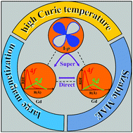
Two-dimensional (2D) ferromagnetic semiconductors (FMSs) exhibit novel spin-dependent electronic and optical properties, opening up exciting opportunities for nanoscale spintronic devices. However, experimentally confirmed 2D FMSs based on transition metal ions are rather limited and their performances are not satisfactory, e.g. typically with low Curie temperatures and small magnetic signals. Different from most known 2D magnets based on d-electrons, here an exotic 2D FMS based on rare-earth ions with f-electrons, a GdI2 monolayer, is predicted to have a large magnetization (8 μB f.u.−1), whose ferromagnetism can survive near room temperature (241 K). In addition, with a small exfoliation energy from its layered van der Waals (vdW) bulk, this GdI2 monolayer holds excellent dynamical and thermal stabilities, making our prediction promising in experiments. Our prediction not only offers a compelling FMS for spintronics, but also provides an alternative route to acquire more high-performance 2D FMSs, going beyond pure d-electron compounds.


New concepts

Two-dimensional (2D) spintronics with the goal of achieving room-temperature Curie temperature (TC) ferromagnetism with large spin polarization, especially ferromagnetic semiconductors (FMSs), are key to the development and application of spintronic devices. However, the currently demonstrated 2D FMSs suffer from rather low Curie temperatures and the magnetic exchange mechanism is unclear. In this work, reported for the first time, a high Curie temperature 2D FMS of rare-earth halides (GdI2 monolayer) is achieved with a number of desirable magnetic properties such as near room-temperature TC, large magnetization, sizable MAE, and good bipolar magnetic semiconductivity. Most interestingly, a new magnetic coupling mechanism in the 2D regime, namely, a d-electron-mediated f–f coupling mechanism, has been proposed. This intriguing magnetism originated from the coexistence of effictive f–f direct-exchange (Gd4f–Gd5d) and super-exchange (Gd5d–(I5p)–Gd5d) interactions. Meanwhile, this monolayer possesses excellent thermal, dynamical, and mechanical stabilities and it has great feasibility of experimental exfoliation from its layered bulk. Our work provides a very promising way to realize a 2D intrinsic room temperature FMS, and will certainly boost the study of 2D rare-earth magnetism.

Spintronic devices, making use of both charge and spin, have generated world-wide interest due to their faster information operation, lower energy consumption, and higher storage density compared to conventional charge-based electronics.1–4 One branch of the most promising candidates for spintronics is ferromagnetic semiconductors (FMSs), which have the advantages of combining conventional semiconductor electronics and nonvolatile magnetic storage at finite temperature.3 FMSs can be used for spin injection, generation, manipulation, and detection, which can be easily implemented in devices by applying nowadays well-developed semiconductor technology.5 Unfortunately, due to the incompatibility between ferromagnetism and semiconductivity, intrinsic FMSs are rare in nature and their Curie temperatures (TC) are usually much lower than room temperature, greatly hindering their practical application.3 Although dilute magnetic semiconductors, which produce ferromagnetism by doping with magnetic elements, were thought to possess potential high-temperature TC, their reproducible TC values are still limited below 200 K (e.g., 155 K for the most successful Mn-doped GaAs).6 Besides, problems such as low spin polarization, low dopant solubility, phase separation, bad controllability, and formation of ferromagnetic (FM) clusters appear difficult to solve.3,5 After many years of studies on dilute magnetic semiconductors, the origin of ferromagnetism in these systems remains a subject of debate.7–9 ‘Is it possible to create magnetic semiconductors that work at room temperature?’ is still one of the most challenging 125 big questions in science in this century.10

The rise of 2D magnetism is expected to have a transformative effect on spintronics applications, such as high integration density and high operation data-processing speed.11–14 For example, the recent discovery of 2D FMSs, including the CrX3 (X = Cl, Br, I) monolayer15,16 and Cr2Ge2Te6 bilayer,17 provides a new playground for applications of 2D spintronics at the nanoscale. Besides these synthesized FMSs, other 2D FMSs have also been predicted based on first-principles calculations, such as CrSBr.18–38 Unfortunately, the TC values of these FMSs are still much below room temperature, although their TC values could be moderately increased by carrier doping,39–41 strain,25,42,43 and electric fields.12,44 Three FMSs were recently predicted to be room-temperature ones;20,45,46 however their corresponding layered vdW bulk crystals are absent.

Rare-earth elements, which typically have large magnetic moments and high magnetocrystalline anisotropy, are very important in both fundamental scientific research as well as real applications of high performance magnets.47–49 However, due to the highly localized characteristic of 4f electrons, the direct overlap of 4f orbitals between neighbor rare-earth elements, as well as the hybridization between 4f orbitals and p orbitals of neighbor anions, is mostly negligible. As a result, the direct exchange and superexchange mediated by anions are usually very weak between rare-earth magnetic elements, which is the most serious drawback in the pursuit of high-temperature 4f magnetism. Therefore, the 4f rare-earth elements seem to be ineffective in the pursuit of high-TC 2D FMSs, and thus no study of 2D 4f magnets has been reported, at least to our best knowledge.

In this work, unexpectedly, we demonstrate the feasibility to realize a promising high-TC FMS of 2D rare-earth halides (GdI2 monolayer). The unique exception comes from the coexistence of spin polarized 5d orbitals and 4f orbitals in Gd2+. The combination of strong Gd4f–Gd5d interactions within each Gd2+ ion and strong Gd5d–(I5p)–Gd5d interactions leads to strong ferromagnetism in the 2D limit, i.e. high-TC (∼241 K), large magnetization (∼8 μB f.u.−1), and large magnetic anisotropy energy (∼553 μeV Gd−1). This work not only takes advantage of the properties of rare-earth elements with large magnetic moment, but also overcomes the weakness of localized f orbital magnetic exchange in 2D magnetism.

The reason we choose the GdI2 monolayer is as follows. Among all rare-earth elements, Gd is the only room-temperature ferromagnetic rare-earth metal, and some of its compounds also possess high Curie temperatures, such as 352 K for GdScSi.50 The FM GdI2 bulk has also been first synthesized by Mee and Corbett51 with room-temperature TC (300–340 K).52–54 In the FM GdI2 bulk, each Gd ion is caged within an I6 trigonal prism (Fig. 1a). It has a layered vdW 2H-MoS2-type structure, in which the I–Gd–I sandwich layers are stacked together along the c-axis in an AB stacking sequence (Fig. S1a, ESI). The electron localization function (Fig. S1b, ESI) confirms that GdI2 is made up of weak vdW bonded I–Gd–I units, which makes it possible for a GdI2 monolayer to be exfoliated from its layered bulk. Meanwhile, the interlayer FM coupling should be very weak due to the relatively large distance between two interlayer nearest-neighbor Gd atoms (7.84 Å, Fig. S1, ESI). This weak interlayer interaction also makes it possible for this monolayer to maintain the room-temperature TC of the FM bulk crystal.


image file: d0mh00183j-f1.tif
Fig. 1 (a) Top and side views of the GdI2 monolayer. (b) Calculated exfoliation energy vs. separation distance (dd0), where d0 indicates the vdW gap between adjacent layers in the bulk crystal. (c) Evolution of the total energy from AIMD simulations and the inset is the structure of the GdI2 monolayer at the end of the AIMD simulation after 10 ps. (d) Phonon dispersion of the GdI2 monolayer.

To explore the possibility of exfoliation of a GdI2 monolayer from its layered bulk crystal, we calculate the cleavage energy from a 4-layer slab. As shown in Fig. 1b, the energy increases with increasing separation distance (dd0), and converges to 0.26 J m−2, which is notably less than the experimental value of graphite (0.36 J m−2),55 suggesting the experimental feasibility. Fig. 1c shows the corresponding fluctuations of the total potential energies for the GdI2 monolayer during the ab initio molecular dynamics (AIMD) simulations and the snapshots of the geometries after annealing at 300 K for 10 ps. The small fluctuations of the energy and integrity of the original configuration with time evolution confirm its good thermal stability. The absence of imaginary modes in the whole Brillouin zone establishes the dynamic stability of the GdI2 monolayer as well (Fig. 1d). Besides, the GdI2 monolayer also meets the mechanical stability Born criteria,56 and it has good in-plane stiffness (ESI). The small cleavage energy and good stabilities strongly support that the 2D GdI2 monolayer could possibly be prepared in experiment and survive at room temperature.

The excellent stability and large feasibility of experimental exfoliation of the GdI2 monolayer inspire us to explore its magnetic and electronic properties. The 2 × 2 supercell of the GdI2 monolayer with various magnetic orders as schematically shown in Fig. S2 (ESI) is considered to determine the magnetic ground state. Our calculations show that the GdI2 monolayer has a FM ground state with an energy difference between the FM and AFM states of 139 meV Gd−1. The spin density presented in Fig. S2 (ESI) indicates that the ferromagnetism mainly comes from the contribution of the Gd ion. Spin-polarized DFT calculations using different exchange–correlation functionals show that the GdI2 monolayer is a semiconductor with an indirect band gap of 0.62 eV (PBE + U) and 1.21 eV (HSE06) (Fig. 2a and b). Note that the HSE06 and PBE + U functionals produce quite similar band structures except for the size of the band gap. The spin–orbit coupling (SOC) effect is also considered and it only decreases the band gap a little bit (Fig. S3, ESI). Detailed analysis of different atomic components reveals that the conduction and valence bands near the Fermi level are dominated by the Gd atom (Fig. 2). Very interestingly, the GdI2 monolayer shows a typical bipolar magnetic semiconductor (BMS) feature,57 in which the valence and conduction bands possess opposite spin-polarization orientation when approaching the Fermi level. Simply by adjusting the position of the Fermi level, the unique electronic structure in the BMS enables the feasibility to achieve half-metallicity, which can provide 100% spin-polarized current.58–60 Clearly, completely spin-polarized currents with reversible spin polarization can be created and controlled by applying a gate voltage, which can be easily applied locally in contrast to magnetic fields.


image file: d0mh00183j-f2.tif
Fig. 2 Atom-resolved electronic band structures of the GdI2 monolayer calculated at the PBE + U (a) and HSE06 (b) levels with the corresponding orbital-projected density of states (c).

The calculated spin-polarized atom-projected and orbital-projected density of states (Fig. 2c and Fig. S4, ESI) further reveals that the magnetism in the GdI2 monolayer is mainly contributed by both 4f and 5d orbitals of Gd atoms. All spin-up 4f orbitals are occupied while the spin-down ones remain empty (Fig. S4, ESI). The narrow and high peaks in the DOS plot indicate that the 4f electrons of Gd are highly localized. Meanwhile, the 5d orbitals are also split into the lower and upper manifolds, which are separated by about 1 eV near the Fermi level. The chemical bonding makes the completely occupied I 5p orbitals mainly centered at ∼4 eV below the Fermi level, which are barely affected by the 4f states. Fig. 2c shows that the top of the valence band is primarily attributed to Gd 5d states, hybridized weakly with I 5p states.

Because the 4f orbitals on Gd atoms are highly localized, their direct participation in magnetic exchange coupling should be negligible. In order to understand the nature of FM coupling in the GdI2 monolayer, intra- and inter-atomic interactions need to be considered. For the intratomic interactions, the wave function of 5d electrons is more extended than that of 4f electrons. Meanwhile, the intratomic Hund interactions between 4f and 5d electrons are strong. As a result, the 5d electrons are spin-polarized in the vicinity of the Fermi level (Fig. 2c) and the 4f moments will align in a cooperative fashion via the surrounding polarized 5d electrons, resulting in intrinsic large magnetic moments.61 For the interatomic coupling, the ferromagnetic order can be determined by the coexistence of the direct- and super-exchange interactions. On one hand, the trigonal prismatic crystal field splits 5d orbitals into three groups, a (dz2), e1 (dxy, dx2y2), and e2 (dxz, dyz) (Fig. 3a). Then one 5d electron will occupy the spin-up channel in the lowest-energy singlet dz2, making the GdI2 monolayer a magnetic semiconductor. In light of Kramers’ mechanism, the partially occupied states will lead to the FM direct-exchange interaction (Gd5d–Gd5d) between the nearest neighboring Gd spins. On the other hand, the bond angle of Gd5d–I5p–Gd5d, θ (∼82.2°), is close to 90°, which also prefers FM coupling according to the Goodenough–Kanamori–Anderson (GKA) rules.62–64 The schematic of the Gd–I–Gd super-exchange interaction mediated by I anions is plotted in Fig. 3b, which arises from the p–d hybridization between I 5p and Gd 5d orbitals. As a result, the effective 4f–4f interaction is FM, mediated by the 5d–(5p)–5d exchanges.


image file: d0mh00183j-f3.tif
Fig. 3 (a) Trigonal prism of six I ions surrounding the Gd ion. (b and c) Schematics of the Gd–I–Gd superexchange path via d–p–d orbitals with the nearest Gd–Gd distance d1, Gd–I distance d2, and Gd–I–Gd bond angle θ.

Magnetic anisotropy is an important requirement for realizing long-range ferromagnetic ordering.65 Magnetic anisotropy can be scaled by the MAE, which directly correlates with the thermal stability of magnetic data storage. Calculations of total energies including SOC are therefore performed on the GdI2 monolayer to estimate the MAE along the x (100), y (010), and z (001) directions as summarized in Table S1 (ESI). As a result, this monolayer maybe exhibits an easy magnetic xy plane. The angular dependence of the MAE is presented in Fig. 4a, which clearly shows that the MAE strongly depends on the direction of magnetization in the xz and yz planes, whereas the MAE is isotropic in the xy plane. As a result, we observe a strong dependence of the MAE on the out-of-plane angle of magnetization, similar to that for the VS2 and FeCl2 monolayers,66,67 and in contrast to the easy axis for the Fe3GeTe268 and CrI315 monolayers. The strong magnetic anisotropy in this monolayer is further confirmed as shown in Fig. 4b, in which the corresponding MAE through the whole space is displayed. The MAE is zero in plane and reaches a maximum of 553 μeV Gd−1 perpendicular to the plane, which is comparable to that of the CrI3 monolayer (685 μeV Cr−1) and larger than those of CrXTe3 (X = Si, Ge, Sn) monolayers (209, 110, 69 μeV Cr−1).29


image file: d0mh00183j-f4.tif
Fig. 4 Angular dependence of the magnetic anisotropic energy (MAE) of the GdI2 monolayer with the direction of magnetization lying on three different planes (a) and the whole space (b). The magnetic moment M (red), specific heat Cv (blue), and magnetic susceptibility χ (green) as functions of temperature for the GdI2 monolayer (c).

T C is another key parameter for the practical application of spintronic devices. Monte Carlo (MC) simulations with the Heisenberg model were performed to estimate the TC of the GdI2 monolayer. The spin Hamiltonian is defined as

image file: d0mh00183j-t1.tif
where J is the nearest neighbor exchange parameter, S is the spin vector of each atom, and A is an anisotropy energy parameter (more details can be found in our previous work22,40,69). A large 50 × 50 supercell is used. Using the energy difference between AFM and FM (139 meV Gd−1) and normalized S (|S| = 1), the estimated Heisenberg exchange parameter J is 34.79 meV from ΔE = EAFMEFM = 4J. After the system reaches equilibrium at a given temperature, the specific heat capacity Cv is calculated by image file: d0mh00183j-t2.tif Given the exact solution to the spin Hamiltonian, TC can be estimated from the peak positions of specific heat Cv or magnetic susceptibility χ. The calculated magnetic moment M, Cv, and χ as functions of temperature for the GdI2 monolayer are illustrated in Fig. 4c, respectively. It can be seen that TC for the GdI2 monolayer is as high as 241 K, which is significantly higher than that of previously reported 2D intrinsic FMS monolayers from their vdW bulk crystals experimentally or theoretically based on the data collected with our utmost endeavor as shown in Fig. S5 (ESI). Meanwhile, using the same approach, our calculated TC values for the recently synthesized CrCl3, CrBr3, and CrI3 monolayers are around 27 K, 40 K, and 43 K (Fig. S6, ESI), respectively, which are in excellent agreement with the experimental values of 17 K,70,71 34 K,16 and 45 K,15 respectively. Note that the estimated TC based on the Ising model can be as high as 745 K (Fig. S7, ESI), which is significantly overestimated due to infinite MAE as assumed in the Ising model. The coexistence of near room-temperature ferromagnetic ordering and semiconducting behavior enables the GdI2 monolayer to be a promising candidate for spintronic applications.

As we point out above, the synergetic effect of direct- and super-exchange interactions determines the magnetic ground state of the GdI2 monolayer. The distance d1 and angle θ play an important role in this exchange mechanism. Besides, the intrinsic physical properties would be also affected by the substrate due to the lattice-mismatch-induced strain in the experimental process. Therefore, it is desirable to investigate the effect of the strain and carrier doping on the magnetic behavior. Fig. 5a and c show the curves of ΔE, d1, and θ under the compression and tension strain. ΔE decreases slightly while d1 and θ increase as the strain is increased. The increased d1 weakens the direct exchange while the increased angle θ (from 82.2° to 85.1°) enhances the super-exchange interaction according to the GKA rule.72 For the compressive strain, however, ΔE increases while d1 and θ decrease as the strain is increased. The decreased d1 makes the direct exchange become more important in determining the FM ordering. On the other hand, the bond angle θ of Gd–I–Gd increases monotonically as well and deviates from 90°, and thus the super-exchange interaction becomes weak. Importantly, in the range of strain investigated, the near room-temperature TC and the BMS characteristic of the GdI2 monolayer are well preserved (Fig. S8 and S9, ESI, respectively). The stabilities and possible phase transformation of the GdI2 monolayer under strain are also discussed (Fig. S10, ESI). For carrier doping, ΔE changes slightly when the hole concentration increases, while it gradually decreases when the electron concentration increases (Fig. 5b). Meanwhile, d1 and the angle θ increase with increasing electron or hole concentration (Fig. 5d). With increasing carrier doping concentration, the GdI2 monolayer undergoes a BMS to half-metal transition (Fig. S11, ESI). Meanwhile, in the range of hole doping, the near room-temperature TC of the GdI2 monolayer is also well preserved (Fig. S12, ESI), while TC decreases a little with increasing electron doping (Fig. S13, ESI).


image file: d0mh00183j-f5.tif
Fig. 5 (a) Strain and (b) carrier dependence of the exchange energy ΔE = EAFM− EFM per unit cell for the GdI2 monolayer. The nearest Gd–Gd distance d1 and Gd–I–Gd bond angle θ as a function of strain (c) and carrier doping (d).

In summary, we have demonstrated a promising way to achieve a 2D FMS by a d-electron-mediated f–f magnetic coupling mechanism. Owing to the effective f–f exchange interactions, a promising 2D intrinsic FMS with near room-temperature TC (241 K) was predicted as realized in the GdI2 monolayer by using first-principles calculations. The FM states, semiconductivity, and the near room-temperature TC can be well maintained under strain conditions. Meanwhile, the GdI2 monolayer possesses BMS properties and provides completely spin-polarized currents with reversible spin-polarization simply by applying a gate voltage. Considering the excellent dynamical and thermal stability, and the fact that its cleavage energy is even smaller than that of graphene, the GdI2 monolayer could be fabricated by mechanical cleavage like graphene. However, we have to point out that the nature of magnetism in a monolayer with an easy magnetic xy plane still remains an open question, as 2D xy magnetism is not expected to show long-range order at finite temperature. Considering the fact that two-dimensional materials are usually synthesized on a substrate, a suitable substrate (such as in heterointerface engineering) might facilitate the synthesis of a GdI2 monolayer, although it is still very challenging, in the future. Our findings not only provide new insights into the magnetic exchange in rare-earth halides at the nanoscale, but also give opportunities for future spintronic investigations and applications.

Method

All the calculations were performed based on spin-polarized density functional theory (DFT) with the Perdew–Burke–Ernzerhof (PBE) functional in the generalized gradient approximation (GGA)73 as implemented in the Vienna ab initio simulation package (VASP).74 The projector-augmented plane wave (PAW) approach was used to represent the ion–electron interaction,75 and the plane-wave cutoff energy was set to 500 eV. Structures were fully relaxed until the force and the energy were converged to 0.01 eV Å−1 and 10−6 eV, respectively. The standard pseudopotential for Gd containing 18 electrons was used, and the 5s25p64f75d16s2 valence-electron configuration was considered. Spin–orbit coupling (SOC) has been included in the calculations because of heavy elements. Specific parameters of U = 9.2 eV and J = 1.2 eV were used for the Gd 4f orbitals, which were adopted from previous work76,77 and successfully reproduce the experimental magnetic moment of Gd ions in bulk GdI2. A detailed test on Ueff (Ueff = UJ) can be found in Fig. S14 (ESI). The HSE06 hybrid functional78 was also employed to obtain a more accurate band structure and verifies the GGA + U method. We have to point out that, in most cases, the electronic and magnetic properties of 4f electron systems are hard to treat due to the strong correlation and strong spin–orbit coupling of very localized f bands.79 However, Gd2+ as studied in our work is an exception, whose 4f orbitals are half-filled, i.e. 4f.7 Such half-filled 4f bands are simple in physics and can be well-treated from first principles. The comparison between FM and AFM states is added as shown in Fig. S15 (ESI). Spin–orbit coupling was included to get the MAE calculation. Phonon dispersions were calculated by density functional perturbation theory embedded in the Phonopy software.80 AIMD simulations in the NVT ensemble using the Nosé–Hoover thermostat lasted for 10 ps with a time step of 1.0 fs.81

Conflicts of interest

The authors declare no competing financial interest.

Acknowledgements

This work is supported by the National Key Research and Development Program of China (2017YFA0204800), Natural Science Funds of China (21525311, 11834002, 11674055), and the Fundamental Research Funds for the Central Universities (2242019R10021). The authors are thankful for the computational resources from the Big Data Center of Southeast University and National Supercomputing Center in Tianjin.

References

  1. X. Li and J. Yang, Wiley Interdiscip. Rev.: Comput. Mol. Sci., 2017, 7, e1314 Search PubMed.
  2. A. Fert, Rev. Mod. Phys., 2008, 80, 1517–1530 CrossRef CAS.
  3. Y. P. Feng, L. Shen, M. Yang, A. Wang, M. Zeng, Q. Wu, S. Chintalapati and C.-R. Chang, Wiley Interdiscip. Rev.: Comput. Mol. Sci., 2017, 7, e1313 Search PubMed.
  4. Y. Zhao, J. J. Zhang, S. Yuan and Z. Chen, Adv. Funct. Mater., 2019, 29, 1901420 CrossRef.
  5. X. Li and J. Yang, Natl. Sci. Rev., 2016, 3, 365–381 CrossRef CAS.
  6. K. Sato, L. Bergqvist, J. Kudrnovský, P. H. Dederichs, O. Eriksson, I. Turek, B. Sanyal, G. Bouzerar, H. Katayama-Yoshida, V. A. Dinh, T. Fukushima, H. Kizaki and R. Zeller, Rev. Mod. Phys., 2010, 82, 1633–1690 CrossRef CAS.
  7. T. Dietl, Nat. Mater., 2010, 9, 965–974 CrossRef CAS PubMed.
  8. A. Zunger, S. Lany and H. Raebiger, Physics, 2010, 3, 53 CrossRef.
  9. T. Dietl and H. Ohno, Rev. Mod. Phys., 2014, 86, 187–251 CrossRef CAS.
  10. Science, 2015, 309, 78–102 Search PubMed.
  11. C. G. a. X. Zhang, Science, 2019, 363, eaav4450 CrossRef PubMed.
  12. H. Li, S. Ruan and Y. J. Zeng, Adv. Mater., 2019, 31, 1900065 CrossRef PubMed.
  13. Y. Zhao, J. Gu and Z. Chen, Adv. Funct. Mater., 2019, 29, 1904782 CrossRef CAS.
  14. S. Zhang, R. Xu, W. Duan and X. Zou, Adv. Funct. Mater., 2019, 29, 1808380 CrossRef.
  15. B. Huang, G. Clark, E. Navarro-Moratalla, D. R. Klein, R. Cheng, K. L. Seyler, D. Zhong, E. Schmidgall, M. A. McGuire, D. H. Cobden, W. Yao, D. Xiao, P. Jarillo-Herrero and X. Xu, Nature, 2017, 546, 270–273 CrossRef CAS PubMed.
  16. Z. Zhang, J. Shang, C. Jiang, A. Rasmita, W. Gao and T. Yu, Nano Lett., 2019, 19, 3138–3142 CrossRef CAS PubMed.
  17. C. Gong, L. Li, Z. Li, H. Ji, A. Stern, Y. Xia, T. Cao, W. Bao, C. Wang, Y. Wang, Z. Q. Qiu, R. J. Cava, S. G. Louie, J. Xia and X. Zhang, Nature, 2017, 546, 265–269 CrossRef CAS PubMed.
  18. N. Miao, B. Xu, L. Zhu, J. Zhou and Z. Sun, J. Am. Chem. Soc., 2018, 140, 2417–2420 CrossRef CAS PubMed.
  19. Y. Zhao, L. Lin, Q. Zhou, Y. Li, S. Yuan, Q. Chen, S. Dong and J. Wang, Nano Lett., 2018, 18, 2943–2949 CrossRef CAS PubMed.
  20. C. Huang, J. Feng, F. Wu, D. Ahmed, B. Huang, H. Xiang, K. Deng and E. Kan, J. Am. Chem. Soc., 2018, 140, 11519–11525 CrossRef CAS PubMed.
  21. Z. Jiang, P. Wang, J. Xing, X. Jiang and J. Zhao, ACS Appl. Mater. Interfaces, 2018, 10, 39032–39039 CrossRef CAS PubMed.
  22. Y. Guo, Y. Zhang, S. Yuan, B. Wang and J. Wang, Nanoscale, 2018, 10, 18036–18042 RSC.
  23. S. Zheng, C. Huang, T. Yu, M. Xu, S. Zhang, H. Xu, Y. Liu, E. Kan, Y. Wang and G. Yang, J. Phys. Chem. Lett., 2019, 10, 2733–2738 CrossRef CAS PubMed.
  24. H. Yin, C. Liu, G. P. Zheng, Y. Wang and F. Ren, Appl. Phys. Lett., 2019, 114, 192903 CrossRef.
  25. H. Y. Lv, W. J. Lu, X. Luo, X. B. Zhu and Y. P. Sun, Phys. Rev. B, 2019, 99, 134416 CrossRef CAS.
  26. C. Wang, X. Zhou, L. Zhou, N.-H. Tong, Z.-Y. Lu and W. Ji, Sci. Bull., 2019, 64, 293–300 CrossRef CAS.
  27. J. He, G. Ding, C. Zhong, S. Li, D. Li and G. Zhang, J. Mater. Chem. C, 2019, 7, 5084–5093 RSC.
  28. C. Huang, Y. Du, H. Wu, H. Xiang, K. Deng and E. Kan, Phys. Rev. Lett., 2018, 120, 147601 CrossRef PubMed.
  29. H. L. Zhuang, Y. Xie, P. R. C. Kent and P. Ganesh, Phys. Rev. B: Condens. Matter Mater. Phys., 2015, 92, 035407 CrossRef.
  30. W.-B. Zhang, Q. Qu, P. Zhu and C.-H. Lam, J. Mater. Chem. C, 2015, 3, 12457–12468 RSC.
  31. X. Li and J. Yang, J. Mater. Chem. C, 2014, 2, 7071 RSC.
  32. V. V. Kulish and W. Huang, J. Mater. Chem. C, 2017, 5, 8734–8741 RSC.
  33. Y. Zhu, X. Kong, T. D. Rhone and H. Guo, Phys. Rev. Mater., 2018, 2, 081001(R) CrossRef.
  34. Q. Wu, Y. Zhang, Q. Zhou, J. Wang and X. C. Zeng, J. Phys. Chem. Lett., 2018, 9, 4260–4266 CrossRef CAS PubMed.
  35. M. Kan, J. Zhou, Q. Sun, Y. Kawazoe and P. Jena, J. Phys. Chem. Lett., 2013, 4, 3382–3386 CrossRef CAS PubMed.
  36. T. Xiao, G. Wang and Y. Liao, Chem. Phys., 2018, 513, 182–187 CrossRef CAS.
  37. Z. Sun, H. Lv, Z. Zhuo, A. Jalil, W. Zhang, X. Wu and J. Yang, J. Mater. Chem. C, 2018, 6, 1248–1254 RSC.
  38. N. Mounet, M. Gibertini, P. Schwaller, D. Campi, A. Merkys, A. Marrazzo, T. Sohier, I. E. Castelli, A. Cepellotti, G. Pizzi and N. Marzari, Nat. Nanotechnol., 2018, 13, 246–252 CrossRef CAS PubMed.
  39. S. Jiang, L. Li, Z. Wang, K. F. Mak and J. Shan, Nat. Nanotechnol., 2018, 13, 549–553 CrossRef CAS PubMed.
  40. B. Wang, Q. Wu, Y. Zhang, Y. Guo, X. Zhang, Q. Zhou, S. Dong and J. Wang, Nanoscale Horiz., 2018, 3, 551–555 RSC.
  41. C. Wang, X. Zhou, Y. Pan, J. Qiao, X. Kong, C.-C. Kaun and W. Ji, Phys. Rev. B, 2018, 97, 245409 CrossRef.
  42. L. Webster and J. A. Yan, Phys. Rev. B, 2018, 98, 144411 CrossRef CAS.
  43. N. Sethulakshmi, A. Mishra, P. M. Ajayan, Y. Kawazoe, A. K. Roy, A. K. Singh and C. S. Tiwary, Mater. Today, 2019, 27, 107–122 CrossRef CAS.
  44. Z. Wang, T. Zhang, M. Ding, B. Dong, Y. Li, M. Chen, X. Li, J. Huang, H. Wang, X. Zhao, Y. Li, D. Li, C. Jia, L. Sun, H. Guo, Y. Ye, D. Sun, Y. Chen, T. Yang, J. Zhang, S. Ono, Z. Han and Z. Zhang, Nat. Nanotechnol., 2018, 13, 554–559 CrossRef CAS PubMed.
  45. C. Huang, J. Feng, J. Zhou, H. Xiang, K. Deng and E. Kan, J. Am. Chem. Soc., 2019, 141, 12413–12418 CrossRef CAS PubMed.
  46. X. Li and J. Yang, J. Am. Chem. Soc., 2019, 141, 109–112 CrossRef CAS PubMed.
  47. J. Jensen and A. R. Mackintosh, Rare earth magnetism, Clarendon Press, Oxford, 1991 Search PubMed.
  48. B. Tyszka and J. Szade, J. Alloys Compd., 2003, 354, 64–71 CrossRef CAS.
  49. L. Roy and T. Hughbanks, J. Solid State Chem., 2003, 176, 294–305 CrossRef CAS.
  50. S. Gupta and K. G. Suresh, J. Alloys Compd., 2015, 618, 562–606 CrossRef CAS.
  51. J. E. Mee and J. D. Corbett, Inorg. Chem., 1965, 4, 88–93 CrossRef CAS.
  52. A. Taraphder, M. S. Laad, L. Craco and A. N. Yaresko, Phys. Rev. Lett., 2008, 101, 136410 CrossRef CAS PubMed.
  53. M. Ryazanov, A. Simon and R. K. Kremer, Phys. Rev. B: Condens. Matter Mater. Phys., 2008, 77, 104423 CrossRef.
  54. A. Kasten, P. H. Moller and M. Schienle, Solid State Commun., 1984, 51, 919–921 CrossRef CAS.
  55. R. Zacharia, H. Ulbricht and T. Hertel, Phys. Rev. B: Condens. Matter Mater. Phys., 2004, 69, 155406 CrossRef.
  56. R. C. Andrew, R. E. Mapasha, A. M. Ukpong and N. Chetty, Phys. Rev. B: Condens. Matter Mater. Phys., 2012, 85, 125428 CrossRef.
  57. X. Li, X. Wu, Z. Li, J. Yang and J. G. Hou, Nanoscale, 2012, 4, 5680–5685 RSC.
  58. H. Cheng, J. Zhou, M. Yang, L. Shen, J. Linghu, Q. Wu, P. Qian and Y. P. Feng, J. Mater. Chem. C, 2018, 6, 8435–8443 RSC.
  59. Y. Wan, Y. Sun, X. Wu and J. Yang, J. Phys. Chem. C, 2018, 122, 989–994 CrossRef CAS.
  60. J. He, G. Ding, C. Zhong, S. Li, D. Li and G. Zhang, Nanoscale, 2019, 11, 356–364 RSC.
  61. L. E. Roy, Rules for understanding rare-earth magnetic compounds, Texas A&M University, 2006 Search PubMed.
  62. J. B. Goodenough, Phys. Rev., 1955, 100, 564–573 CrossRef CAS.
  63. J. Kanamori, J. Appl. Phys., 1960, 31, S14–S23 CrossRef.
  64. P. W. Anderson, Phys. Rev., 1959, 115, 2–13 CrossRef CAS.
  65. N. D. Mermin and H. Wagner, Phys. Rev. Lett., 1966, 17, 1133–1136 CrossRef CAS.
  66. H. L. Zhuang and R. G. Hennig, Phys. Rev. B, 2016, 93, 054429 CrossRef.
  67. M. Ashton, D. Gluhovic, S. B. Sinnott, J. Guo, D. A. Stewart and R. G. Hennig, Nano Lett., 2017, 17, 5251–5257 CrossRef CAS PubMed.
  68. H. L. Zhuang, P. R. C. Kent and R. G. Hennig, Phys. Rev. B, 2016, 93, 134407 CrossRef.
  69. B. Wang, Y. Zhang, L. Ma, Q. Wu, Y. Guo, X. Zhang and J. Wang, Nanoscale, 2019, 11, 4204–4209 RSC.
  70. X. Cai, T. Song, N. P. Wilson, G. Clark, M. He, X. Zhang, T. Taniguchi, K. Watanabe, W. Yao, D. Xiao, M. A. McGuire, D. H. Cobden and X. Xu, Nano Lett., 2019, 19, 3993–3998 CrossRef CAS PubMed.
  71. H. H. Kim, B. Yang, S. Li, S. Jiang, C. Jin, Z. Tao, G. Nichols, F. Sfigakis, S. Zhong and C. Li, Proc. Natl. Acad. Sci. U. S. A., 2019, 116, 11131–11136 CrossRef CAS PubMed.
  72. K. Junjiro, J. Phys. Chem. Solids, 1959, 10, 87–98 CrossRef.
  73. J. P. Perdew, K. Burke and M. Ernzerhof, Phys. Rev. Lett., 1996, 77, 3865–3868 CrossRef CAS PubMed.
  74. G. Kresse and J. Furthmüller, Phys. Rev. B: Condens. Matter Mater. Phys., 1996, 54, 11169–11186 CrossRef CAS PubMed.
  75. P. E. Blöchl, Phys. Rev. B: Condens. Matter Mater. Phys., 1994, 50, 17953–17979 CrossRef PubMed.
  76. P. Larson, W. R. L. Lambrecht, A. Chantis and M. van Schilfgaarde, Phys. Rev. B: Condens. Matter Mater. Phys., 2007, 75, 045114 CrossRef.
  77. H. Jamnezhad and M. Jafari, J. Comput. Electron., 2017, 16, 272–279 CrossRef CAS.
  78. J. Heyd, G. E. Scuseria and M. Ernzerhof, J. Chem. Phys., 2003, 118, 8207–8215 CrossRef CAS.
  79. M. Casadei, X. Ren, P. Rinke, A. Rubio and M. Scheffler, Phys. Rev. Lett., 2012, 109, 146402 CrossRef PubMed.
  80. X. Gonze and C. Lee, Phys. Rev. B: Condens. Matter Mater. Phys., 1997, 55, 10355–10368 CrossRef CAS.
  81. G. J. Martyna, M. L. Klein and M. Tuckerman, J. Chem. Phys., 1992, 97, 2635–2643 CrossRef.

Footnote

Electronic supplementary information (ESI) available: The structure and ELF of the GdI2 bulk; Mechanical stability of the GdI2 monolayer; spin density of FM and AFM states; band structure with SOC, density of states, and MAE for the GdI2 monolayer; relationship between the band gaps and Curie temperature in monolayer 2D ferromagnetic semiconductors; magnetic moment as functions of temperature for 2D FM CrCl3, CrBr3, and CrI3, respectively; magnetic moment, magnetic susceptibility, and specific heat as functions of temperature for the GdI2 monolayer based on the Ising model; band structure of the GdI2 monolayer under −4% and 4% strain; magnetic moment, magnetic susceptibility, and specific heat as functions of temperature for the GdI2 monolayer under −4% and 4% strain; stability and relative energy of the GdI2 monolayer under different strains; band structure and Curie temperature of the GdI2 monolayer under different carrier doping concentrations; energy difference of the GdI2 monolayer under different Ueff values; density of states for a single Gd atom in the FM and AFM states. See DOI: 10.1039/d0mh00183j

This journal is © The Royal Society of Chemistry 2020