
 Open Access Article
 This Open Access Article is licensed under a
 Creative Commons Attribution 3.0 Unported Licence
Beyond graphene oxide: laser engineering functionalized graphene for flexible electronics†
Raul D.
Rodriguez
 *a,
Alimzhan
Khalelov
a,
Pavel S.
Postnikov
ab,
Anna
Lipovka
a,
Elena
Dorozhko
a,
Ihsan
Amin
*c,
Gennadiy V.
Murastov
a,
Jin-Ju
Chen
d,
Wenbo
Sheng
e,
Marina E.
Trusova
a,
Mohamed M.
Chehimi
f and
Evgeniya
Sheremet
*a
*a,
Alimzhan
Khalelov
a,
Pavel S.
Postnikov
ab,
Anna
Lipovka
a,
Elena
Dorozhko
a,
Ihsan
Amin
*c,
Gennadiy V.
Murastov
a,
Jin-Ju
Chen
d,
Wenbo
Sheng
e,
Marina E.
Trusova
a,
Mohamed M.
Chehimi
f and
Evgeniya
Sheremet
*a
aTomsk Polytechnic University, Lenina Ave. 30, 634034, Tomsk, Russia. E-mail: raul@tpu.ru; esheremet@tpu.ru
bDepartment of Solid State Engineering, Institute of Chemical Technology, 16628 Prague, Czech Republic
cVan’t Hoff Institute of Molecular Science, University of Amsterdam, Science Park 904, 1098 XH Amsterdam, The Netherlands. E-mail: i.amin@uva.nl
dSchool of Materials and Engineering, University of Electronic Science and Technology of China, 610054 Chengdu, China
eLeibniz Institute of Polymer Research Dresden e.V., Hohe Str. 6, 01069, Dresden, Germany
fUniversité Paris Est, UMR 7182 CNRS, UPEC, 94320, Thiais, France
First published on 4th February 2020
Abstract
Carbon nanomaterials, especially graphene, are promising due to their abundance and the possibility to exploit them in lightweight, flexible, and wearable electronics enabling paradigms such as the Internet of Things. However, conventional methods to synthesize and integrate graphene into functional materials and flexible devices are either hazardous, time demanding, or excessively energy-consuming. To overcome these issues, here we propose a new concept based on the laser processing of single-layer diazonium-functionalized graphene. This is a safe, inexpensive, and environmentally-friendly method making it a competitive alternative for graphene-device fabrication. Flexible chemiresistors exhibit sensitivity for breath (water vapor and CO2) and ethanol detection up to 1500% higher than laser-reduced graphene oxide devices. We attribute this enhanced sensitivity to an optimal balance between structural defects and electrical conductivity. Flexible electronic circuits demonstrate a superb resilience against scratching and high current stability up to 98% with durability against 180° bending cycles for continuous operation of several weeks. This work can impact biomedical technology and electronics where tunable electrical conductivity, sensitivity, and mechanical stability are of uttermost importance.
New conceptsGraphene is the most researched nanomaterial of the XXI century. However, there are still limitations to its wide-spread integration in flexible electronics. For these applications, graphene has to be produced, isolated, dispersed, deposited, and further processed into functional devices. To tackle this bottleneck here we show a new and highly efficient approach for the integration of functionalized graphene into a robust, flexible, water-stable, and electrically conductive nanostructures. This is possible with our method based on the one-step exfoliation and chemical functionalization with laser processing. In contrast to GO-based technology, our method is environmentally-friendly, safe, with low energy consumption, and straightforwardly applicable to flexible devices. Our process is unlike the usual oxidation–reduction cycle of laser-reduced GO, involving a reduction–oxidation process due to sp3 oxidation by laser processing. In applications, our devices show a high performance compared to those made with the state-of-the-art water-dispersible graphene source: graphene oxide, reduced by laser irradiation. The superior chemical sensitivity, as well as the unprecedented mechanical stability of our materials, made possible the development of scratch-resistant flexible devices with high electrical and mechanical stability for several weeks of operation. We found that the unprecedented properties of our material are due to the polymer–graphene composite formation and to the balance between defect concentration and electrical conductivity. |
Introduction
There is a global and ever-growing demand for wearable, foldable, and stretchable electronics in the energy, environmental monitoring and medical sectors to name but a few.1–3 The chosen technology must provide spatially-defined control of the conductivity type and value, electrical contacts, and a dielectric material. Moreover, the materials have to be non-toxic, flexible, and stable at the pH of body sweat for wearable electronics. There are carbon nanomaterials that can fulfill those specifications. These materials include graphene, reduced graphene oxide, carbon nanotubes, and graphene–conductive polymer composites.4–6 Graphene-based materials have challenges for industrial and wide-spread applications beyond university labs, which is one of the objectives we would like to see realized.7 Graphene oxide (GO) offers two significant advantages that allow a new range of applications. Robotics, sensors, wearables, power generation, electronics, catalysis, and chemical protection are a few of the plethora of applications that show graphene oxide becoming a strong player in these fields.8–12 The first advantage of GO is its excellent water dispersibility and low-cost. The second one is the tunability of its physical and chemical properties by controlling the number of oxygen-containing groups that depends on the degree of reduction. Increasing the reduction of GO gives way to reduced graphene oxide (rGO), an electrical conductor of potentially-high importance in electronic applications, including wearable technology and advanced textiles.13 The common ways to reduce GO involve electrons,14 photons,15 heat,16 or the use of reducing agents in chemical reduction processes.17 On the one hand, the thermal and chemical routes suffer from different issues, in particular, the lack of spatial control of the reduction process. On the other hand, electron-based processing suffers from other problems, such as limited scalability necessary for large-area fabrication. In contrast, the laser reduction process does not have these issues. In addition to the spatial control of reduction using photons from a tightly focused laser beam, the laser reduction is also cleaner than any chemical method and more energy-efficient than thermal annealing. This versatility and compatibility make the laser-irradiation and graphene oxide an excellent combination for developing novel electronics attracting significant attention from researchers around the world in recent years.18–21 Laser processing can also be adapted easily to lithography. This versatility is essential considering that UV photolithography is still the gold-standard for wafer-scale patterning in microelectronics. GO is typically obtained by using strong acids and oxidizing agents that introduce oxygen-containing groups between the planes of the graphite precursor.22–26 In addition to explosion risks and toxicity, the conventional chemical methods, based on Hummer's approach depicted in Fig. 1a, necessarily implies the degradation of graphene properties due to the strong disruption of conjugated carbon lattice system. These issues with the Hummer's approach motivated the development of variations and improvements of that make GO production safer and more efficient.27 Herein, as an alternative to GO, we propose a novel paradigm for developing graphene-laser irradiated flexible devices. Our concept illustrated in Fig. 1a, in comparison to laser-reduced GO, is based on the reductive exfoliation of graphite with the formation of modified graphene sheets followed by laser irradiation. The photon energy induces the oxidation of functionalized graphene layers via the elimination of aryl groups. The graphitic nature of our graphene material is demonstrated in the analyses below. As a starting point, we built on previous reports that show the one-step covalent exfoliation and functionalization of single-layer graphene with diazonium salts. A significant demonstration was provided by Englert et al.,28 who used diazonium salts to functionalize graphene in bulk quantities. In 2017, two groups working independently reported the single-step electrochemical exfoliation and functionalization of graphene with diazonium salts.29,30 Now, for the first time, we demonstrate the applicability of diazonium-functionalized graphene (herein called Mod-G) to create insulating films that can be turned conductive by laser irradiation. We thus create a novel, scalable, green, safe, and sustainable way to produce graphene-based electronics (see chemical structural changes depicted in Fig. S1, ESI†).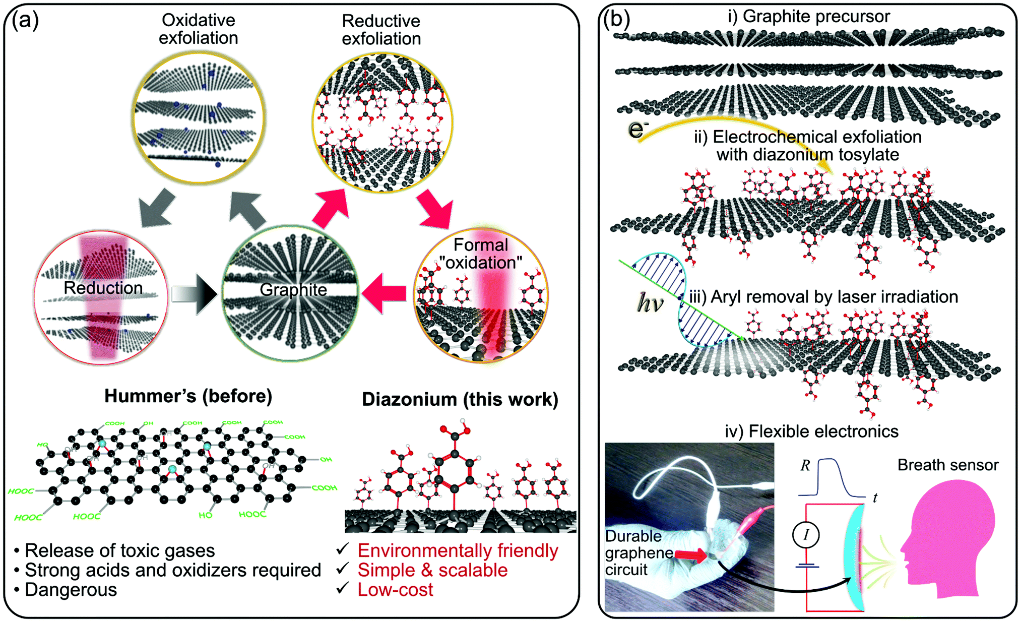 | ||
| Fig. 1 (a) A comparative depiction of the graphene cycle from exfoliation of bulk graphite to the laser reduction and partial reconversion to sp2 carbon. At the left is the conventional method based on graphene oxide by Hummers’ method, and at the right side is our approach using an electrochemical-based diazonium method with photothermal and photochemical processing by laser irradiation. The graphitic nature of Mod-G during the whole process is demonstrated in the sections below. (b) Schematics of the Mod-G generation from (i) a graphite precursor, (ii) aryl functionalization, (iii) removal by laser irradiation, and (iv) applications in flexible electronics including a flexible breath chemiresistor device. | ||
Laser-processing was previously used to improve the properties of multilayer graphene films on glass. Del et al. showed a decrease in surface roughness and sheet resistance while increasing optical transparency by almost two-fold after using laser processing.31 In contrast, Claussen's group exploited pulsed UV laser irradiation of GO films to increase the film surface roughness and 3D texturing in petal-like shapes. Such laser-induced film structuring increased the electrochemical activity of paper-based electrodes made by inkjet-printed GO.32 They pushed that research further by increasing the electroactive surface area of graphene films in the form of pores using a combined salt porogen for micropore formation and laser annealing to form smaller submicrometer-sized pores.33 All these examples show the powerful, large-scale, and low-cost application of laser-processing graphene for optimized flexible electronics and sensors. This study presents the novel integration of laser processing as an essential step in the conductivity change of functionalized graphene, from insulating to conducting, and inducing a strong interaction and possible encapsulation with the polymer substrate providing unprecedented mechanical and environmental stability.
The electrochemical exfoliation of graphene sheets was carried out using the modified procedure described by Belanger.29 Thus, as the source of diazo-cations, we applied stable, non-explosive, and water-soluble 4-carboxybenzenediazonium tosylate34 containing the –COOH group. This functionalization offered improvements such as long-term stability in water dispersions for modified graphene which is key for solution-processable fabrication. The described modification allows implementing the electrochemical exfoliation readily with the formation of large quantities of graphene flakes in aqueous media.
We demonstrate the proof-of-concept application of laser-irradiated Mod-G (LMod-G‡) films by fabricating conductive circuits on flexible and rigid substrates and chemiresistor for gas sensors (see illustration in Fig. 1b). Our devices show long-term stability and higher sensitivity compared to those based on conventional laser-reduced GO films used here as reference systems. With this communication, we describe a new technology to extend graphene-like materials to flexible, wearable, and light-weight consumer electronics. Moreover, our method based on room-temperature laser processing is compatible with polymers and other temperature-sensitive materials.
As illustrated in Fig. 1b, the uniqueness and novelty of this work are the combinations of a water-soluble, stable, and safe diazonium tosylate and graphene with electrochemical and photonic methods. In this way, we produce devices with much higher performance and mechanical stability than the state-of-the-art based on laser-reduced GO or even silver inks. This superb performance contributes to making graphene an irreplaceable material technology.7
Results
Single-layer nature, formation, and electronic properties of Mod-G
Single-layer diazonium-functionalized graphene sheets were obtained by electrochemical exfoliation of a graphite electrode in the presence of diazonium salt as depicted in Fig. 2a (see also Fig. S1a, ESI† and current vs. time changes during exfoliation in Fig. S1b, ESI†). The experimental details are presented in the ESI.† The nanoscale structural characterization using several AFM methods evidences the presence of single-layer Mod-G. Fig. 2b shows a large contrast for the surface potential image obtained by KPFM. The contact potential difference (CPD) in KPFM gives information about the work function for metallic samples, and electronic doping and charge-transfer in semiconductors by nullifying the electrostatic force between a biased tip and the sample.35 In our samples, the CPD is dominated by two clearly distinctive regions visible in the histogram approximated by two Gaussian fits in Fig. 2c. These two regions correspond to one with higher CPD value for HOPG at around 21 mV while the other region has a CPD centered at −30 mV for the Mod-G film. The change in surface potential from graphite to Mod-G is a consequence of the strong perturbation to the electronic structure of graphene and subsequent doping due to the covalent grafting of aryl groups as previously shown in the case of graphite as well as non-covalent functionalization by diazonium salts.36 The KPFM surface potential image in Fig. 2b shows that HOPG appears positive while the Mod-G appears negative, as well as the patches marked by the arrows. This was confirmed by a zoom-in around those regions making isolated Mod-G layers like the one shown in Fig. 2d visible. The layer thickness determined from the cross-sectional analysis in the inset of Fig. 2d is 1.1 nm, which is comparable to the thickness of GO. The 1.1 nm thickness for Mod-G is higher than the 0.3 nm thickness of single-layer graphene. As illustrated schematically by inset (i) of Fig. 1b, this larger size is due to aryl groups making a graphene sandwich. We also performed the electrochemical production of Mod-G in a single drop. We illustrate this process in Fig. 3a. For this experiment, we used a freshly-cleaved graphite electrode as the substrate and source of graphene with a ≅0.2 mL drop of diazonium solution in 0.1 M sulfuric acid. We set a potential difference of 10 V between an Au microwire counter electrode used as cathode and the HOPG substrate. The AFM topography image in Fig. 3b shows the HOPG electrode surface after electrochemical exfoliation. The surface is characterized by ribbon-like structures visible in the zoom-in in Fig. 3c. The AFM height line profiles show that these ribbons correspond to single-layer Mod-G. A larger blister-like structure of about 32 nm in height appears at the intersection of the exfoliated stripes in Fig. 3b. This figure also shows two clean stripes of HOPG converging at the vertices of a blister-like structure at the left side and the “burst blister” location at the right. An electrically-biased tip in AFM generates an electrostatic tip-sample force. This force detected at the second-harmonic of cantilever excitation gives rise to DFM.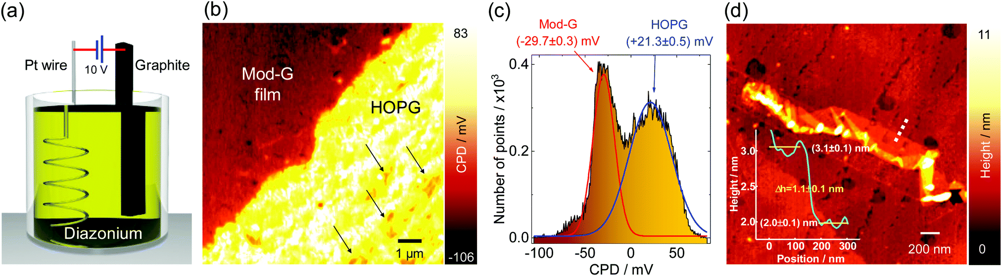 | ||
| Fig. 2 (a) Sketch (non-scaled) of the graphene exfoliation in diazonium salt drop deposited on a freshly-cleaved graphite (HOPG) substrate electrode. (b) Kelvin probe force microscopy image of the interface between a Mod-G film and HOPG obtained after drop-coating using a Mod-G dispersion obtained from electrochemical exfoliation. (c) Surface potential histogram analysis of (b) showing the distribution between HOPG and Mod-G fitted by Gaussian functions showing the CPD positions and standard deviation values. The few regions with negative surface potential on the lower-right side of the CPD image (marked with arrows) show some Mod-G deposited on the HOPG side. (d) AFM zoom-in image on the lower-right side of (b) showing a monolayer graphene flake of about 1.1 nm thickness deduced from the cross-section in the inset. | ||
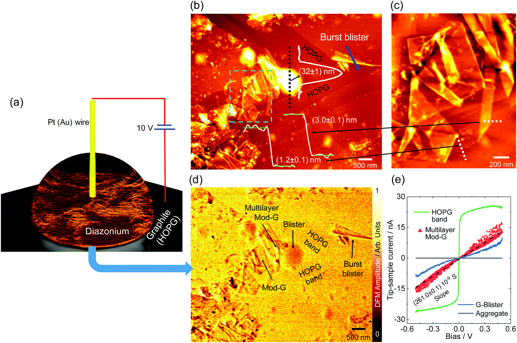 | ||
| Fig. 3 (a) Sketch (non-scaled) of the graphene exfoliation in diazonium salt drop deposited on freshly-cleaved graphite (HOPG) substrate electrode. (b) AFM height image of the HOPG electrode after exfoliation in the presence of diazonium salt. The height profiles indicate the presence of single layers, ribbons, and a blister-like structure. (c) A zoom-in image on the ribbon monolayer graphene exfoliated from the bulk HOPG substrate. (d) Dielectric force microscopy image acquired simultaneously to the topography in (b). (e) I–V curves from different regions marked by arrows in (c). | ||
In a non-contact fashion, DFM allows mapping with nanoscale resolution the electronic properties of a sample, including carrier concentration, doping, and charge carrier mobility.34
The DFM image in Fig. 3d was simultaneously recorded with the topography image in Fig. 3b, showing regions with different dielectric force. From DFM results in Fig. 3d, we identify two regions with brighter and darker contrast. The darker regions correspond to single-layer Mod-G, Mod-G aggregates, and the blister-like structure in the microscopy images. In the same DFM experimental session, we obtained in situ localized conductance from different regions of interest marked by arrows in Fig. 3d (and Fig. S2, ESI† for the aggregate). In Fig. 3e, we show the IV curves from those locations. One of the most crucial results from DFM capacitance microscopy and IV characterization is that the HOPG bands have much higher conductance than Mod-G ribbons and blisters. This result implies that HOPG bands are not functionalized.
Contrary to HOPG bands, exfoliated single-layer graphene ribbons and blisters are functionalized as evidenced by the capacitance image contrast indicating lower conductivity.37 Therefore, these observations lead us to conclude that the graphene ribbons in Fig. 3b and c were original parts of the HOPG bands. These bands were peeled off starting from the burst blister location marked in Fig. 3b. These are unique insights on Mod-G formation dynamics leading us to propose that the blisters are an intermediary state to the exfoliation of graphene.
Similar blister structures of different sizes were visible everywhere on the graphite substrate as partly shown in Fig. S2 (ESI†). The origin of these blisters is related to the electrochemical decomposition of water that results in gas generation, graphene bubbling, and subsequent exfoliation after the blisters burst open. This assertion is supported by the nanoscale IV curve electrical characterization in Fig. 3e. The IV curve obtained from the blister shows higher current stability than multilayer Mod-G. This behaviour is related to an imperfect conductance path made by the more disordered functionalized graphene. We can infer that the blister is a non-functionalized graphene bubble, and thus aryl functionalization only occurs after graphene layers are exfoliated from graphite, not before. Understanding and controlling the exfoliation and functionalization of Mod-G are critical to the technological application of this material. Basically, the oxygen groups are useful for any further functionalization in a wide range of applications such as membranes with controllable water flow38 or as impermeable barriers for the case of GO when it is mildly reduced.39
Conductivity and surface microstructure of laser-irradiated Mod-G
We hypothesized that laser processing would allow the selective modification of Mod-G similarly to the laser-patterning approach used to make conductive devices out of GO films.40 For this, we proceeded with the investigation of devices built on an electrically insulating glass substrate.One of the essential parameters of materials for optoelectronics and sensor applications is electrical conductivity. Therefore, here we show C-AFM results on LMod-G. The picture shown in Fig. 4 is an actual photograph of the sample and experimental contacts used to obtain the results shown in Fig. 4a–d. The nanoscale topography in Fig. 4a shows that the disk-shaped LMod-G film on glass has a thickness of ca. 2.7 μm. The current map in Fig. 4b highlights the uniform conductance of the LMod-G film. This LMod-G map contrasts the inhomogeneous conductance from the rGO film (see Fig. S3, ESI†). For the sake of comparison, both LMod-G and rGO were prepared in the same way using identical laser irradiation conditions. The large LMod-G structure in Fig. 4c has a size of over 3 μm deduced from cross-section analysis in Fig. 4d. The IV curve made on this large structure shows a surprising ohmic behavior even at this relatively large micrometer scale. This result has important implications for LMod-G application in electronics by minimizing losses and improving charge collection and injection. Consider also that it is not so usual obtaining ohmic contacts from a highly functionalized graphene material.41 The ohmic behavior and low resistance of LMod-G support our initial hypothesis that the laser-irradiation can restore the sp2 hybridization to aryl functionalized graphene sheets. Contrary to laser-reduced GO, the laser irradiation of Mod-G can be considered a formal “oxidation” of covalently-modified graphene. Laser irradiation then leads to the formation of graphene sheets with lower sp3 carbon content as schematically illustrated in Fig. S1c (ESI†). The LMod-G conductance of 275.8 × 10⁻⁹ S obtained from the IV curve analysis in Fig. 4d is comparable to the 261.0 × 10⁻⁹ S value for the Mod-G layer in Fig. 3e. Although these conductance values are similar, assuming the same AFM tip size, we can conclude that both materials have entirely different conductivity. This conclusion is justified considering the large thickness different for each case responsible for the electrical conductance. Indeed, the bilayer Mod-G is 3 nm thick while the LMod-G structure has a height of about 2.7 μm that is already covered by an LMod-G film 3.2 μm thick. In addition to these long paths for charge-carrier transport, a millimeter-scale LMod-G is connecting that structure to an external electrode. This comparison illustrates the sharp conductivity change that the laser irradiation makes in Mod-G films. We also verified the macro-scale conductance of LMod-G that became conductive only after the laser irradiation step, as shown by IV characterization results in Fig. S4 (ESI†). IR spectroscopy results from Mod-G and LMod-G films on Kapton in Fig. S5 (ESI†) confirm that the conductivity change after laser irradiation is related to the removal of aryl groups. This conclusion is based on the absence of O–H vibrations in the IR spectrum of LMod-G in Fig. S5 (ESI†) and also by X-ray photoelectron spectroscopy (XPS) results in Fig. S6 (ESI†).
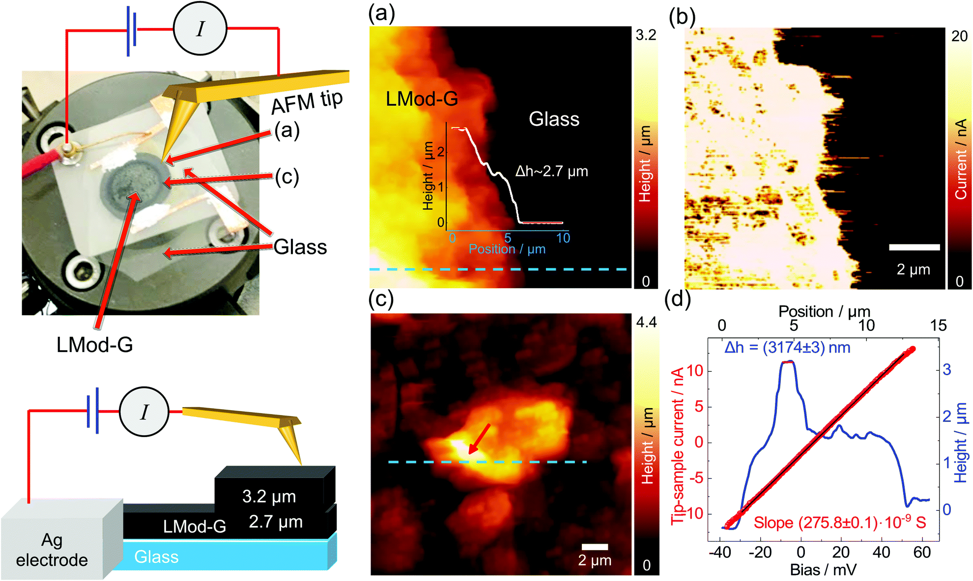 | ||
| Fig. 4 (Left panel) Photograph of the actual experimental configuration used for (a) to (d), the LMod-G circular film is shown by an arrow and the CSAFM experiment diagram is shown on the bottom inset. (a) Topography and (b) current mapping of laser-irradiated Mod-G (LMod-G) on a glass substrate. (c) Topography and (d) cross-section of a large aggregate on the LMod-G region. The IV curve obtained at the tallest point marked by an arrow in (c) shows still a good conductance of 275.8 × 10⁻⁹ S. | ||
In summary, we showed that Mod-G films make a packed system composed of layers with 1.1 nm thickness. However, these single layers are not only graphene but a graphene sandwich with aryl groups covering the top and bottom planes, as shown schematically in Fig. 1b (inset ii). This aryl functionality gives a good homogeneity to Mod-G also in films (see a Mod-G/graphite interface in Fig. S7, ESI†). Under the influence of an external potential, electrons are not able to overcome the barrier made by aryl molecules. The high resistance for non-irradiated Mod-G implies that not even charge-hopping takes place for Mod-G aggregates, as shown by the IV curves in Fig. 3e. Only after the aryl groups get removed by laser irradiation, the electrons are free to flow through the LMod-G film. In these conditions, the whole film becomes electrically conductive with a charge-transport dominated by electron scattering with defects like in the case of highly-reduced GO.41 The ohmic-like behavior with the top contact electrode made of Au in the form of an AFM tip shows promise for hybrid electronic applications with enhanced charge injection and collection.
Raman spectroscopy analysis
Besides the electrical characterization of LMod-G, we performed Raman spectroscopy to follow the structural and chemical changes that occurred before and after laser irradiation. Raman hyperspectral imaging results for thin Mod-G and LMod-G layers on glass show a strong contribution from the glass substrate (see Fig. S8, ESI†). To minimize the signal contribution from glass, we investigated several types of graphene-based materials shown schematically in the inset in Fig. 5.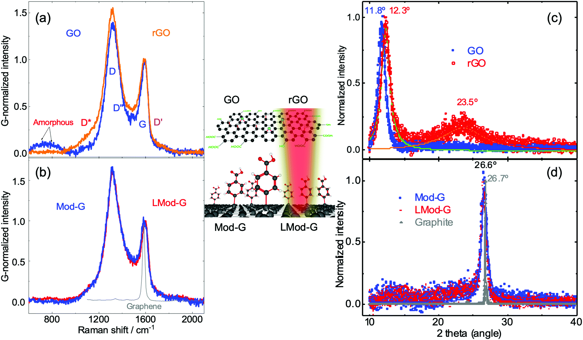 | ||
Fig. 5 Mid-inset: Sketch of the four types of graphene materials studied by Raman spectroscopy and X-Ray diffraction, GO and Mod-G and their laser-processed counterparts, rGO and LMod-G. (a) Raman spectra comparison for GO and laser-reduced GO films. (b) Raman spectra of Mod-G and laser-irradiated Mod-G (LMod-G). The Raman spectrum from single-layer graphene is included in (b) as a reference of purely sp2 hybridized carbon. (c) X-ray diffraction of the as-deposited GO and laser-reduced GO (rGO). (d) X-ray diffractograms of Mod-G laser-irradiated Mod-G (LMod-G). The graphite result used as the reference for C![[double bond, length as m-dash]](https://www.rsc.org/images/entities/char_e001.gif) C sp2 is taken from RUFF Database, RRUFF ID: R050503.1. The experimental data were fitted with a Lorentzian function. The fitting standard error was below 0.1 degrees. C sp2 is taken from RUFF Database, RRUFF ID: R050503.1. The experimental data were fitted with a Lorentzian function. The fitting standard error was below 0.1 degrees. | ||
These samples correspond to films used in actual devices further examined below. Fig. 5a shows the Raman spectra of pristine GO and rGO films. Except for the G band, the other bands correspond to defect-activated modes in GO.42 The bands below 800 cm−1 originate from amorphous carbon.43 In contrast to mechanically-exfoliated graphene with a relatively small defect concentration, a lower D/G ratio for GO represents a higher amount of defects. This high defect concentration range corresponds to stage 2, following the terminology introduced by Ferrari and Robertson.44 The X-ray diffraction analysis below confirms the lower crystallinity of all graphene-based samples with respect to graphite. The increase in the D/G ratio for more graphitic materials was previously observed for highly-reduced GO.17 Therefore, we can use the D/G intensity ratio and the D band sharpness as measures of crystallinity and lattice order. We can then order these graphene materials by decreasing crystallinity in this way: LMod-G ≅ Mod-G > rGO > GO. This observation further confirms that our method to produce graphene is less drastic than the conventional method based on graphene oxide. This assertion is valid for either form, oxidized (GO), or even reduced (rGO). Fig. 5b shows the Raman spectra from pristine and laser-irradiated Mod-G. The spectrum for single-layer graphene is also included as a reference of a purely sp2 atomically thin carbon system.
The spectral differences can be made more evident by fitting the Raman spectra shown in Fig. S9 (ESI†). We chose to fit with five peaks D*, D, D′′, G, and D′ bands following the work by Claramunt et al.42 for the evaluation of oxygen content in GO. However, a limitation of this fitting approach is the significant uncertainties in the peak position determination for the D* and D′′, which are precisely the ones expected to correlate to the oxygen content. Although the bandwidth for LMod-G is slightly smaller than for Mod-G in agreement with a crystallinity increase, this change in D band sharpness is within the error bars, see Fig. S9c and d (ESI†). Nevertheless, from the Raman peak position analysis of non-irradiated and irradiated Mod-G, we found that the D* and D bands upshift that can be related to changes in oxidation and defects.42 In our case, the laser irradiation of Mod-G induces completely different oxidation changes to the case of GO; therefore, we need to be careful when comparing these two cases.
X-ray diffraction: the graphitic nature of Mod-G and LMod-G
X-ray diffraction (XRD) was used to assess the effect of laser irradiation on the crystallinity of diazonium-modified graphene. For GO, after reduction, the 2θ diffraction peak around 11° due to (002) planes decreases, giving rise to a graphitic peak around 23.5°, as seen in Fig. 5c. This makes XRD a convenient way to determine the reduction changes in GO.45 The upshift of the (002) diffraction peak in rGO is due to the decrease in lattice constant after water molecules and oxygen-containing groups were removed. However, this is different for Mod-G. The XRD results in Fig. 5d show no difference for Mod-G and LMod-G, where both are characterized by a sharp 2θ peak at 26.7°. The graphite diffractogram is plotted as the reference of an ideal sp2 carbon system. The peak sharpness is the main difference between the Mod-Gs and graphite, and this can be correlated to the degree of crystallinity. This peak is not expected in single-layer graphene since a 3D crystal stacking is needed to have Bragg reflections. In our case, we see this peak due to the powder form of Mod-G after dried in the air forming graphitic aggregates. The broadening of the peak can be attributed to this disordered layered system stacked in 3D, where the signal to noise ratio decreases for the Mod-Gs. Therefore, Mod-G is shown to be of graphitic nature although highly disordered, with the laser irradiation making an insignificant effect on crystallinity. These results also support the insignificant changes observed for the D band sharpness in the Raman spectroscopic results for Mod-G and LMod-G in Fig. 5b. By comparing XRD results with previous reports, Mod-G crystallinity appears higher than for other graphene-based materials obtained by electrochemical exfoliation.45,46 This result is significant since controlling disruptions to the sp2 carbon lattice is desirable to exploit the most the electronic properties of graphene.Applications of laser-irradiated Mod-G: a gas sensor and a flexible solar-powered circuit
We fabricated chemiresistors from the same device shown in Fig. 4 as proof of principle of potential applications. We made the rGO- and LMod-G-based chemiresistors in Fig. 6a with the same dimensions and electrical contacts, and tested their sensing properties simultaneously under the same conditions. Fig. 6b shows the morphology of LMod-G obtained by SEM. The devices were placed inside a Petri dish for gas sensing experiments. 4 mL of ethanol was inserted at the bottom of the dish that was then covered, as shown in Fig. 6c. The small amount of liquid ethanol did not get into contact with the devices but only ethanol fumes. The resistance for both rGO and LMod-G chemiresistors were simultaneously recorded. The percentage change in resistance is determined as: | (1) |
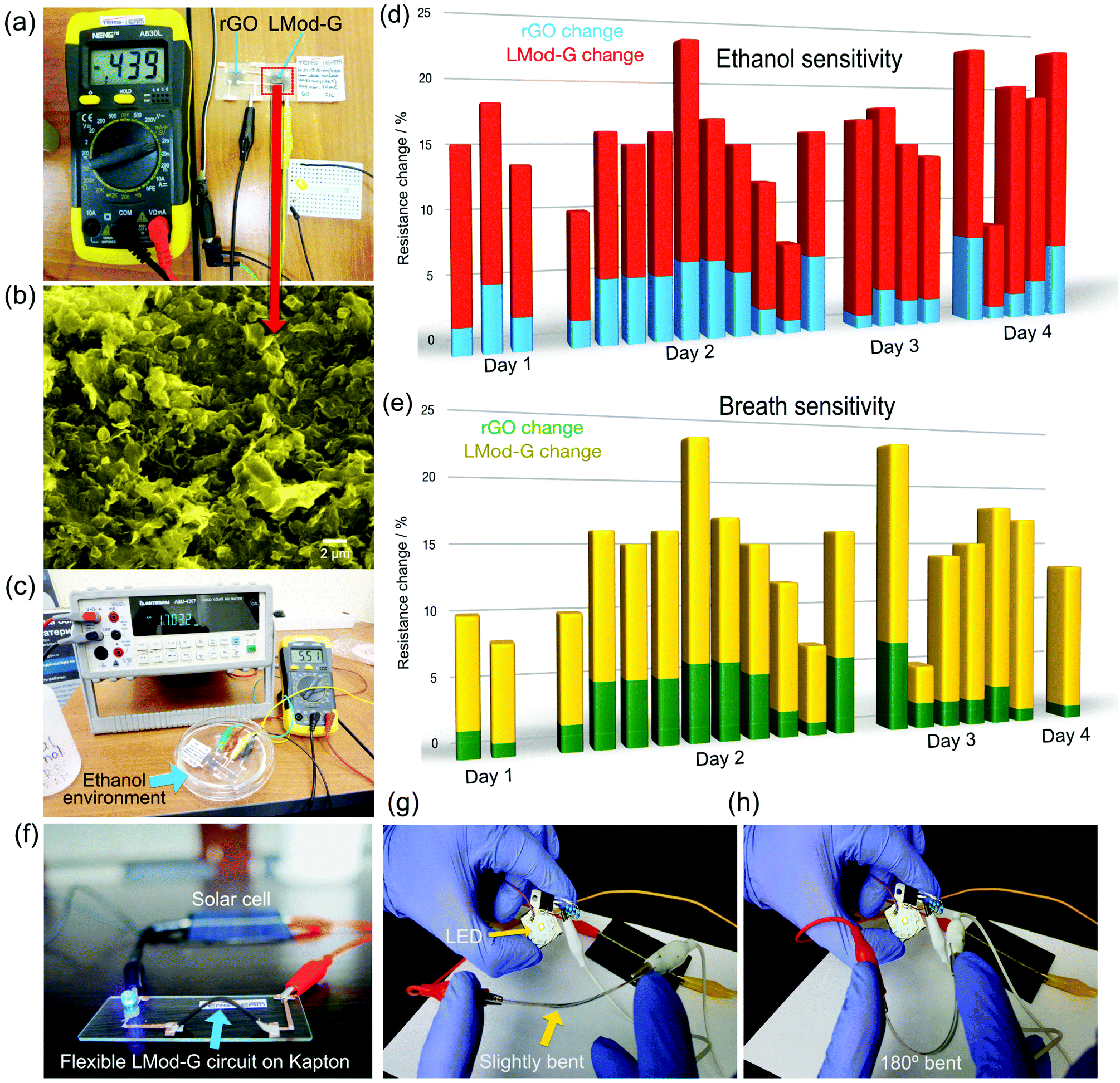 | ||
| Fig. 6 (a) Photograph of rGO and LMod-G devices on the same glass substrate. (b) SEM image of the LMod-G showing the layered material structure. (c) Photograph of the sensor for ethanol sensitivity experiments. Testing results for the rGO and LMod-G devices as chemiresistors for (d) ethanol in the gas phase and (e) human breath. The results are shown in terms of percentual resistance changes for individual measurements over a period of several days. (f) Photograph of LMod-G on Kapton in a solar cell-powered circuit that operated 24/7 for several weeks with high current stability of over 98%. Pictures of an LMod-G flexible device on PET for (g) slightly bent and (h) 180 degrees bent while lightning another LED without drastic changes in conductance. | ||
An LMod-G film on Kapton (LMod-G/Kapton) film shown in Fig. 6f was used as a proof of concept for an application in a flexible device. The LMod-G/Kapton flexible device showed a high performance during continuous operation for 24/7 with current stability of over 98%. We only interrupted the device operation when testing the circuit current for stability evaluation (see Fig. S11, ESI†). Similar to the device on Kapton, LMod-G on PET (LMod-G/PET) was also fabricated. We evaluated the mechanical stability of LMod-G/PET flexible device against deformation, twisting, 180° bending, and mechanical contacting (touching) as illustrated in Fig. S12 (ESI†). From these analyses, we did not observe any performance degradation whatsoever of the LMod-G/PET LED circuit, even when it was in direct contact with water (Fig. S11 and S12, ESI†). We minimized bending the electrical contacts made with the silver paste by directing most of the mechanical deformation to the LMod-G layer. Otherwise, the silver paint contacts would have cracked (see Fig. S12, ESI†). This precaution was necessary for testing without device failure illustrating how LMod-G outperforms silver inks and silver paints. Thus, LMod-G appears now as a better alternative to state-of-the-art conductors for flexible and printed electronics applications. The waterproof capability of LMod-G demonstrated after water immersion experiments is also very promising (see Fig. S12c, ESI†). Added to electrical conductivity and chemical sensitivity, waterproof LMod-G electrodes could be exploited in electrochemistry and electrocatalysis applications. These electrochemical applications now under investigation can be evidenced when comparing our LMod-G electrodes with conventional electrode materials like glassy carbon. Moreover, a clear advantage of LMod-G/PET is outstanding mechanical stability. As demonstrated in the Video S1 (ESI†), LMod-G is stable not just after bending it but even after mechanically scratching it. Neither rGO nor Ag inks show this level of mechanical stability. We hypothesize that the unprecedented mechanical stability of LMod-G on PET is related to a composite formation with the polymer substrate. A detailed investigation of this laser-induced composite is beyond the scope of this work, but it is being reported elsewhere in follow-up work. The reason why LMod-G outperforms rGO in sensors can be related to the right balance between a high defect concentration and high conductivity. The Raman spectroscopy analysis shows that both GO and Mod-G have a large concentration of defects as reflected by the presence of the D band. However, Mod-G has lower structural defects as shown by the sharpness of Raman bands (Fig. S9c and d, ESI†). After laser irradiation, the upshift of the D band in LMod-G implies a further increase in crystallinity as compared to the initial Mod-G. While defects are necessary as active sites for molecular sensing, a too high defect concentration compromises the electrical conductivity degrading the capability of the graphene-based layer to act as a sensor. Therefore, compared to rGO, the homogeneous and high electrical conductivity of LMod-G films with the right defect concentration are behind its superior performance in chemical sensors. We expect that there should be a balance of defects vs. conductivity that optimizes graphene-based films for sensing applications. The role of defects in graphene was already shown to play an essential role in improving these materials for electrochemical sensor applications (for example, see ref. 48 and 49). In this work, we performed a qualitative analysis of defects utilizing Raman spectroscopy and XRD characterization methods. With Raman spectroscopy, the D/G intensity ratio is typically used to quantify defect concentration in graphene and carbon nanotubes.50 However, the conventional D/G ratio analysis does not provide accurate quantitative or even qualitative information in the case of highly defective carbon systems like graphene oxide. This was previously shown in a systematic analysis of defects made by focused ion beams on graphite showing also broad amorphous bands below 1000 cm−1.51 That amorphous signature is exactly what we observe in the case of GO films before laser irradiation (see Raman spectra in Fig. 5a), but not on Mod-G films even without laser irradiation. This amorphous band disappeared after GO films were laser-reduced indicating the partial restoration of crystallographic order in the film. It shows that our modified graphene has a significant amount of defects but not to the high extent of GO films. The XRD results also showed that during the whole electrochemical and photonic processing steps, Mod-G remained graphitic which is essential for a good charge-carrier mobility and therefore conductivity, albeit with a high amount of structural defects needed for chemical sensing. So far, we aimed to optimize the laser irradiation parameters such as power density, pulse duration, and focal distance to maximize the electrical conductance of our LMod-G films. By plotting the second-order Raman modes area vs. laser power we could obtain an idea of the optimal irradiation conditions that maximize conductivity.52 By using those same samples in chemical sensors one could then correlate the electrical conductivity, chemical sensitivity, and crystallinity to determine the best conditions that maximize sensor performance.
Another important property to consider is the surface wettability of the graphene derivate. The film hydrophilicity has strong implications in biomedical applications due to interactions with cells, proteins, and other biomolecules. For example, in the case of graphene oxide, the oxygen-containing groups determine the degree of cell attachment and cell proliferation.53,54 We performed contact angle (CA) measurements to evaluate the surface wettability of Mod-G and GO films and the changes that occurred after laser treatment, see results in Fig. S10 (ESI†). We found that GO shows a hydrophilic behavior with CA values of 38 ± 4° within the range of previous reports.55,56 After laser reduction, the CA values of rGO increase to 60 ± 14° due to the removal of oxygen-containing groups. For the case of Mod-G, we found that the film surface is superhydrophilic with CA values equal to 0°. This superhydrophilicity arises from a strong contribution of carboxylic groups to the wetting process. After irradiation and partial aryl group removal, the material turns to behave the same way as rGO with a CA of 58 ± 10°. This drastic change in wettability after laser irradiation further confirms the successful cleavage of 4-carboxyphenylene groups from Mod-G films.
Discussion and perspectives
The initial exfoliation of graphene was based on the procedure reported by Bélanger29 with a key modification. We used the highly-stable and water-soluble 4-carboxybenzenediazonium tosylate as the source of diazonium cation.34 This diazonium salt allows us to exclude the use of organic solvents. Moreover, the presence of a hydrophilic carboxyl group improves the dispersibility of modified graphene in aqueous solutions for further processing, similar to the oxygen-rich moieties in graphene oxide. This was indeed verified by our experimental observations readily visible in Fig. S13 (ESI†). These observations show that our process gives functionalized graphene layers unprecedented water stability against aggregation. The long-term stability of our samples, up to over seven months at the time of this writing, contrasts the 1 h stability shown by Ossonon and Bélanger29 with anthraquinone-functionalized graphene. The single-layer nature and p-type doping induced by the interaction of aryl radicals with graphene were confirmed by Kelvin probe force microscopy in agreement with a previous report.41 We also anticipate that the laser irradiation provides another degree of freedom for the surface potential and doping control of aryl-functionalized graphene films. This electronic control, combined with organic semiconductors and perovskites, could allow engineering the energy levels and band alignment between different interfaces that are critical for optoelectronics.41,57,58 The spectroscopic comparison between laser-irradiated and non-irradiated Mod-G shows that negligible changes occur to the crystallinity of Mod-G as evidenced by Raman and XRD results. This is completely different from the case of GO that shows significant changes in Raman and XRD. In Mod-G, the sp3 carbon hybridization is introduced as a result of the bonding to aryl groups (Ar), which can be considered as a reduction process (the transformation of Csp2 to Csp3). In the case of graphene oxide, the appearance of sp3 carbon is associated with carbon oxidation with the formation of C–OH or C–O–C moieties. However, for both cases, Raman spectroscopy is sensitive to the formation of Csp3 as evidenced by the large broadening of D and G bands and upshift of the G mode, just like in the case of GO. Interestingly, the electrical resistance of Mod-G changes drastically after laser irradiation making Mod-G an electrically conductive material. Consider the conventional case of rGO that becomes conductive because of the removal of oxygen-containing groups and formal reduction (the transformation of C–OH, CO and C–O–C groups to C–C/CC bonds). Our results show that Mod-G becomes conductive due to a completely different mechanism. Instead, we observe a formal oxidation process – the cleavage of C–Ar bonds followed by the transformation of Csp3 to Csp2 with the restoration of the conjugated carbon structure (see Fig. S1c, ESI†). IR spectroscopy results support this hypothesis (see Fig. S5, ESI†) showing that the laser irradiation induces the removal of aryl groups from the graphene surface. XRD proves that LMod-G remains graphitic, although with a lower degree of crystallinity than graphite as evidenced by the broadening of the carbon 2θ diffraction peak. The laser irradiation does not make a significant difference to Mod-G crystallinity. Therefore, we conclude that the laser makes Mod-G conductive due to the removal of charge-carrier barriers made by aryl groups which is in agreement with our concept illustration in Fig. 1a. The mechanism proposed for the removal of aryl groups involves the thermal homolysis of C–C bonds between graphene and functional groups on the Mod-G surface. This assertion is supported by our XPS results shown in the ESI† as well as by a previous report that shows the thermally-induced cleavage of aryl groups.59 The energy of the laser beam dramatically increases the Mod-G surface temperature, which leads to the cleavage of covalently attached aryl radicals. This is the equivalent to the photothermal reduction of graphene oxide using laser beams. The laser irradiation processing of Mod-G could ultimately allow engineering the charge-injection and interface contact providing another route beyond usual methods based on chemical functionalization.60 Moreover, by introducing an electron-donor or photo-active group to the structure of arenediazonium tosylate it is also possible to provide n-type doping to graphene, additionally enhancing optical properties.61,62 Beyond transport and electrical properties with polymer composites,63 diazonium salt functionalization enhances mechanical and chemical interaction with polymer matrices like shown for the case of rGO.64 Generally, our concept changes the paradigm for the design of graphene-based electronics. Instead of the standard sequence from bulk graphite oxidation followed by laser reduction, we show a novel way starting from reductive exfoliation involving one electron transfer from graphene to the diazonium salt,65 the cleavage of the N2 group with the formation of highly active aryl radicals, and the subsequent covalent graphene functionalization changing Csp2 to Csp3, and the last step with a laser-oxidative process restoring the graphene conjugated system (transformation of Csp3 to Csp2). We illustrate this process in Fig. S1c (ESI†). We found key insights on the formation mechanism of Mod-G by analyzing the HOPG electrode after electrochemical exfoliation. After the HOPG sample was rinsed and dried, the peeled-off regions still partially tethered to the substrate collapsed back forming the ribbons visible in Fig. 3c. This is the first time that the electrode used in the one-step electrochemical exfoliation and functionalization of graphene is directly visualized at the nanoscale providing clues about graphene formation. More details on the mechanism of this exfoliation process must be investigated in follow-up work. As proof-of-principle of some applications, we showed the continuous operation of LMod-G on Kapton in a flexible circuit powered by a solar cell for two months. In dynamic bending, even after over fifty bending cycles at 180°, LMod-G on PET shows remarkable electromechanical stability with no loss of conductivity or circuit breaking. As chemiresistors, during dozens of experiments spanning several days, our sensors made of LMod-G on glass showed superior sensitivity and response time to ethanol and breath in comparison to similar devices made of laser-reduced GO tested under identical conditions. Moreover, as shown in Tables S1 and S2 (ESI†), the LMod-G sensor performance for breath and ethanol is also superior to for chemiresistors made using other carbon-based materials reported before.
Conclusions
We demonstrated a novel and competitive laser- and solution-processable technology for functionalized graphene. Our method is far superior to state-of-the-art devices based on laser-reduced graphene oxide, helping pave the way to the laser-based fabrication of flexible and lightweight electronics. These applications, critical to the implementation of paradigms such as the Internet of Things and wearable health-care devices, can now rely on the ease of fabrication, scalability, unprecedented mechanical stability, and chemical sensitivity of this laser-graphene technology.Conflicts of interest
There are no conflicts to declare.Acknowledgements
We thank Maxim Fatkullin, Vladimir Bogoslovskiy, and Sergey Kim for help with the LMod-G electrodes; Antonkin Nikita for the IR measurements; and Elizaveta Sviridova for the wettability measurements. We are thankful to Mekhman Yusubov for essential support that made this work possible. This research is supported by the Tomsk Polytechnic University within the framework of the Tomsk Polytechnic University Competitiveness Enhancement Program, 5-100, and by the Sichuan Science and Technology Program (Grant 2018HH0152).Notes and references
- T. R. Ray, J. Choi, A. J. Bandodkar, S. Krishnan, P. Gutruf, L. Tian, R. Ghaffari and J. A. Rogers, Chem. Rev., 2019, 119, 5461–5533 CrossRef PubMed.
- H. Huang, S. Su, N. Wu, H. Wan, S. Wan, H. Bi and L. Sun, Front. Chem., 2019, 7, 399 CrossRef PubMed.
- A. Bolotsky, D. Butler, C. Dong, K. Gerace, N. R. Glavin, C. Muratore, J. A. Robinson and A. Ebrahimi, ACS Nano, 2019, 13, 9781–9810 CrossRef PubMed.
- S. Wang, J. Y. Oh, J. Xu, H. Tran and Z. Bao, Acc. Chem. Res., 2018, 51, 1033–1045 CrossRef PubMed.
- J. Heikenfeld, A. Jajack, J. Rogers, P. Gutruf, L. Tian, T. Pan, R. Li, M. Khine, J. Kim, J. Wang and J. Kim, Lab Chip, 2018, 18, 217–248 RSC.
- Y. Zhou, C. Chen, S. Zhu, C. Sui, C. Wang, Y. Kuang, U. Ray, D. Liu, A. Brozena, U. H. Leiste, N. Quispe, H. Guo, A. Vellore, H. A. Bruck, A. Martini, B. Foster, J. Lou, T. Li and L. Hu, Mater. Today, 2019, 30, 17–25 CrossRef.
- L. Lin, H. Peng and Z. Liu, Nat. Mater., 2019, 18, 520–524 CrossRef PubMed.
- Y. Tan, Z. Chu, Z. Jiang, T. Hu, G. Li and J. Song, ACS Nano, 2017, 11, 6843–6852 CrossRef PubMed.
- E. Singh, M. Meyyappan and H. S. Nalwa, ACS Appl. Mater. Interfaces, 2017, 9, 34544–34586 CrossRef PubMed.
- H. Guo, T. Li, X. Cao, J. Xiong, Y. Jie, M. Willander, X. Cao, N. Wang and Z. L. Wang, ACS Nano, 2017, 11, 856–864 CrossRef PubMed.
- J. E. Choe, M. S. Ahmed and S. Jeon, J. Power Sources, 2015, 281, 211–218 CrossRef.
- P.-Y. Chen, M. Zhang, M. Liu, I. Y. Wong and R. H. Hurt, ACS Nano, 2018, 12, 234–244 CrossRef PubMed.
- L. Liu, Y. Yu, C. Yan, K. Li and Z. Zheng, Nat. Commun., 2015, 6, 7260 CrossRef PubMed.
- G. Gonçalves, J. Borme, I. Bdkin, A. González-Mayorga, G. Irurueta, H. I. S. Nogueira, M. C. Serrano, P. Alpuim and P. A. A. P. Marques, Carbon, 2018, 129, 63–75 CrossRef.
- Y. Zhang, L. Guo, S. Wei, Y. He, H. Xia, Q. Chen, H.-B. Sun and F.-S. Xiao, Nano Today, 2010, 5, 15–20 CrossRef.
- Z. Wei, D. Wang, S. Kim, S.-Y. Kim, Y. Hu, M. K. Yakes, A. R. Laracuente, Z. Dai, S. R. Marder, C. Berger, W. P. King, W. A. de Heer, P. E. Sheehan and E. Riedo, Science, 2010, 328, 1373–1376 CrossRef PubMed.
- I. K. Moon, J. Lee, R. S. Ruoff and H. Lee, Nat. Commun., 2010, 1, 73 CrossRef PubMed.
- R. Trusovas, G. Račiukaitis, G. Niaura, J. Barkauskas, G. Valušis and R. Pauliukaite, Adv. Opt. Mater., 2016, 4, 37–65 CrossRef.
- B. Senyuk, N. Behabtu, A. Martinez, T. Lee, D. E. Tsentalovich, G. Ceriotti, J. M. Tour, M. Pasquali and I. I. Smalyukh, Nat. Commun., 2015, 6, 7157 CrossRef PubMed.
- Y. Qiao, Y. Wang, H. Tian, M. Li, J. Jian, Y. Wei, Y. Tian, D.-Y. Wang, Y. Pang, X. Geng, X. Wang, Y. Zhao, H. Wang, N. Deng, M. Jian, Y. Zhang, R. Liang, Y. Yang and T.-L. Ren, ACS Nano, 2018, 12, 8839–8846 CrossRef PubMed.
- R. Ye, D. K. James and J. M. Tour, Acc. Chem. Res., 2018, 51, 1609–1620 CrossRef PubMed.
- SciVee, 2010.
- M. Venkanna and A. K. Chakraborty, AIP Conf. Proc., 2014, 1591(1), 574–576 CrossRef.
- Q. Zheng and J.-K. Kim, Graphene for Transparent Conductors, 2015, pp. 29–94 Search PubMed.
- R. Boveri, Graphene Oxide: Synthesis, Mechanical Properties and Applications, Nova Science Pub Incorporated, 2014 Search PubMed.
- W. Gao, Graphene Oxide, 2015, pp. 1–28 Search PubMed.
- D. C. Marcano, D. V. Kosynkin, J. M. Berlin, A. Sinitskii, Z. Sun, A. Slesarev, L. B. Alemany, W. Lu and J. M. Tour, ACS Nano, 2010, 4, 4806–4814 CrossRef.
- J. M. Englert, C. Dotzer, G. Yang, M. Schmid, C. Papp, J. M. Gottfried, H.-P. Steinrück, E. Spiecker, F. Hauke and A. Hirsch, Nat. Chem., 2011, 3, 279–286 CrossRef.
- B. D. Ossonon and D. Bélanger, Carbon, 2017, 111, 83–93 CrossRef.
- A. Ejigu, I. A. Kinloch and R. A. W. Dryfe, ACS Appl. Mater. Interfaces, 2017, 9, 710–721 CrossRef.
- S. K. Del, R. Bornemann, A. Bablich, H. Schäfer-Eberwein, J. Li, T. Kowald, M. Östling, P. Haring Bolívar and M. C. Lemme, 2D Mater., 2015, 2, 011003 CrossRef.
- S. R. Das, Q. Nian, A. A. Cargill, J. A. Hondred, S. Ding, M. Saei, G. J. Cheng and J. C. Claussen, Nanoscale, 2016, 8, 15870–15879 RSC.
- J. A. Hondred, I. L. Medintz and J. C. Claussen, Nanoscale Horiz., 2019, 4, 735–746 RSC.
- V. D. Filimonov, M. Trusova, P. Postnikov, E. A. Krasnokutskaya, Y. M. Lee, H. Y. Hwang, H. Kim and K.-W. Chi, Org. Lett., 2008, 10, 3961–3964 CrossRef.
- W. Melitz, J. Shen, A. C. Kummel and S. Lee, Surf. Sci. Rep., 2011, 66, 1–27 CrossRef.
- F. M. Koehler, N. A. Luechinger, D. Ziegler, E. K. Athanassiou, R. N. Grass, A. Rossi, C. Hierold, A. Stemmer and W. J. Stark, Angew. Chem., Int. Ed., 2009, 48, 224–227 CrossRef.
- J. Zhang, W. Lu, Y. S. Li, J. Cai and L. Chen, Acc. Chem. Res., 2015, 48, 1788–1796 CrossRef PubMed.
- K.-G. Zhou, K. S. Vasu, C. T. Cherian, M. Neek-Amal, J. C. Zhang, H. Ghorbanfekr-Kalashami, K. Huang, O. P. Marshall, V. G. Kravets, J. Abraham, Y. Su, A. N. Grigorenko, A. Pratt, A. K. Geim, F. M. Peeters, K. S. Novoselov and R. R. Nair, Nature, 2018, 559, 236–240 CrossRef.
- Y. Su, V. G. Kravets, S. L. Wong, J. Waters, A. K. Geim and R. R. Nair, Nat. Commun., 2014, 5, 4843 CrossRef.
- W. Gao, N. Singh, L. Song, Z. Liu, A. L. M. Reddy, L. Ci, R. Vajtai, Q. Zhang, B. Wei and P. M. Ajayan, Nat. Nanotechnol., 2011, 6, 496–500 CrossRef.
- C. Punckt, F. Muckel, S. Wolff, I. A. Aksay, C. A. Chavarin, G. Bacher and W. Mertin, Appl. Phys. Lett., 2013, 102, 023114 CrossRef.
- S. Claramunt, A. Varea, D. López-Díaz, M. Mercedes Velázquez, A. Cornet and A. Cirera, J. Phys. Chem. C, 2015, 119, 10123–10129 CrossRef.
- F. Li and J. S. Lannin, Appl. Phys. Lett., 1992, 61, 2116–2118 CrossRef.
- A. C. Ferrari and J. Robertson, Phys. Rev. B: Condens. Matter Mater. Phys., 2000, 61, 14095–14107 CrossRef.
- P. Cui, J. Lee, E. Hwang and H. Lee, Chem. Commun., 2011, 47, 12370–12372 RSC.
- H.-L. Guo, X.-F. Wang, Q.-Y. Qian, F.-B. Wang and X.-H. Xia, ACS Nano, 2009, 3, 2653–2659 CrossRef.
- L. Guo, Y.-W. Hao, P.-L. Li, J.-F. Song, R.-Z. Yang, X.-Y. Fu, S.-Y. Xie, J. Zhao and Y.-L. Zhang, Sci. Rep., 2018, 8, 4918 CrossRef.
- W. Yuan, Y. Zhou, Y. Li, C. Li, H. Peng, J. Zhang, Z. Liu, L. Dai and G. Shi, Sci. Rep., 2013, 3, 2248 CrossRef.
- J. A. Hondred, I. L. Medintz and J. C. Claussen, Nanoscale Horiz., 2019, 4, 735–746 RSC.
- A. Jorio and L. G. Cançado, Phys. Chem. Chem. Phys., 2012, 14, 15246–15256 RSC.
- R. D. Rodriguez, Z. Khan, B. Ma, A. Mukherjee, P. Meszmer, J. Kalbacova, E. Garratt, H. Shah, J. Heilmann, A. R. Hight Walker, B. Wunderle, E. Sheremet, M. Hietschold and D. R. T. Zahn, Phys. Status Solidi, 2019, 216, 1900055 CrossRef CAS.
- B. Ma, R. D. Rodriguez, A. Ruban, S. Pavlov and E. Sheremet, Phys. Chem. Chem. Phys., 2019, 21, 10125–10134 RSC.
- X. Shi, H. Chang, S. Chen, C. Lai, A. Khademhosseini and H. Wu, Adv. Funct. Mater., 2012, 22, 751–759 CrossRef CAS.
- L. Dedelaite, R. D. Rodriguez, E. Andriukonis, M. Hietschold, D. R. T. Zahn and A. Ramanavicius, Sens. Actuators, B, 2018, 255, 1735–1743 CrossRef CAS.
- S. Wang, Y. Zhang, N. Abidi and L. Cabrales, Langmuir, 2009, 25, 11078–11081 CrossRef CAS.
- R. Rasuli, Z. Mokarian, R. Karimi, H. Shabanzadeh and Y. Abedini, Thin Solid Films, 2015, 589, 364–368 CrossRef CAS.
- T. M. Brenner, D. A. Egger, L. Kronik, G. Hodes and D. Cahen, Nat. Rev. Mater., 2016, 1, 1443 Search PubMed.
- M. Oehzelt, K. Akaike, N. Koch and G. Heimel, Sci. Adv., 2015, 1, e1501127 CrossRef.
- J. M. Englert, C. Dotzer, G. Yang, M. Schmid, C. Papp, J. M. Gottfried, H.-P. Steinrück, E. Spiecker, F. Hauke and A. Hirsch, Nat. Chem., 2011, 3, 279–286 CrossRef CAS PubMed.
- C. Liu, Y. Xu and Y.-Y. Noh, Mater. Today, 2015, 18, 79–96 CrossRef CAS.
- Z. Xia, F. Leonardi, M. Gobbi, Y. Liu, V. Bellani, A. Liscio, A. Kovtun, R. Li, X. Feng, E. Orgiu, P. Samorì, E. Treossi and V. Palermo, ACS Nano, 2016, 10, 7125–7134 CrossRef CAS PubMed.
- X. Zhang, L. Hou and P. Samorì, Nat. Commun., 2016, 7, 11118 CrossRef CAS.
- D. S. Yu, T. Kuila, N. H. Kim and J. H. Lee, Chem. Eng. J., 2014, 245, 311–322 CrossRef CAS.
- J. R. Lomeda, C. D. Doyle, D. V. Kosynkin, W.-F. Hwang and J. M. Tour, J. Am. Chem. Soc., 2008, 130, 16201–16206 CrossRef CAS.
- G. L. C. Paulus, Q. H. Wang and M. S. Strano, Acc. Chem. Res., 2013, 46, 160–170 CrossRef CAS.
Footnotes |
| † Electronic supplementary information (ESI) available. See DOI: 10.1039/c9mh01950b |
| ‡ Mechanical stability of LMod-G flexible circuit after bending and mechanical scratching. https://youtu.be/qHsI8hvWaxM. |
| This journal is © The Royal Society of Chemistry 2020 |