
High-κ polymers of intrinsic microporosity: a new class of high temperature and low loss dielectrics for printed electronics†
Zhongbo
Zhang‡
 a,
Jifu
Zheng‡
b,
Kasun
Premasiri‡
c,
Man-Hin
Kwok
a,
Qiong
Li
a,
Ruipeng
Li
d,
Suobo
Zhang
b,
Morton H.
Litt
a,
Xuan P. A.
Gao
c and
Lei
Zhu
*a
a,
Jifu
Zheng‡
b,
Kasun
Premasiri‡
c,
Man-Hin
Kwok
a,
Qiong
Li
a,
Ruipeng
Li
d,
Suobo
Zhang
b,
Morton H.
Litt
a,
Xuan P. A.
Gao
c and
Lei
Zhu
*a
aDepartment of Macromolecular Science and Engineering, Case Western Reserve University, 2100 Adelbert Road, 44106-7202, USA. E-mail: lxz121@case.edu
bKey Laboratory of Ecomaterials, Changchun Institute of Applied Chemistry, Chinese Academy of Sciences, Changchun 130022, P. R. China
cDepartment of Physics, Case Western Reserve University, 2076 Adelbert Road, Cleveland, Ohio 44106, USA
dNational Synchrotron Light Source II, Brookhaven National Laboratory, Upton, New York 11973, USA
First published on 31st October 2019
Abstract
High performance polymer dielectrics are a key component for printed electronics. In this work, organo-soluble polymers of intrinsic microporosity (PIMs) are reported for the first time to demonstrate desirable dielectric properties with a high permittivity (or κ), heat resistance, and low dielectric loss simultaneously. Due to the highly dipolar sulfonyl side groups (4.5 D) and rigid contorted polymer backbone, a sulfonylated PIM (SO2-PIM) enabled friction-free rotation of sulfonyl dipoles in the nanopores. As such, an optimal balance between relatively high κ and low dielectric loss is achieved in a broad temperature window (−50–200 °C). For example, the discharged energy density reached 17 J cm−3 with κ = 6.0. The discharge efficiency was 94% at 150 °C/300 MV m−1 and 88% at 200 °C/200 MV m−1. Furthermore, its application as a high-κ gate dielectric in field effect transistors (FETs) is demonstrated. With the bilayer SO2-PIM/SiO2 gate dielectric, InSe FETs exhibited a high electron mobility in the range of 200–400 cm2 V−1 s−1, as compared to 40 cm2 V−1 s−1 for the bare SiO2-gated InSe FET. This study indicates that highly dipolar PIMs with a rigid polymer backbone and large free volume are promising as next generation gate dielectric materials for printed electronics.
New conceptsIn this work, a new concept of a friction-free dipolar glass polymer is demonstrated using novel sulfonylated polymers of intrinsic microporosity (SO2-PIMs). First, the nanopores in PIMs provide large free volume for friction-free rotation of side-chain dipolar groups. Second, the sulfonyl group has a large dipole moment of 4.5 D to promote orientational polarization. Third, the rigid, contorted, ladder-like backbone of PIM enables a high glass transition temperature (Tg, above the thermal degradation temperature). As a result of friction-free rotation of sulfonyl dipoles in the nanopores below the Tg, SO2-PIM shows a dissipation factor as low as 0.005, while achieving a high dielectric constant (κ = 6) and a high discharged energy density of 17 J cm−3 with discharge efficiency >90% at room temperature. Even at 175 °C, the discharge efficiency maintained at 86%, indicating excellent heat tolerance. Compared to existing high κ dipolar polymers, this concept has never been demonstrated before. Furthermore, the dielectric performance of SO2-PIM is tested in the InSe field-effect transistors (FETs). Intriguingly, the high κ SO2-PIM significantly promotes the electron mobility in InSe to 200–400 cm2 V−1 s−1. This work demonstrates that SO2-PIMs are promising as next generation gate dielectric materials for printed electronics. |
High-dielectric constant (or high-κ) and low-loss polymer dielectrics are highly desirable for power and electronic applications, including electric energy storage1–3 and printed electronics4,5 such as in human performance monitoring,6 information storage devices,7 and soft robotics.8 One important component for all hybrid electronic devices is the organic field effect transistor (FET), where high-κ/low-loss gate dielectrics play an important role.9–12 The state-of-the-art gate dielectric used in industry is self-assembled monolayer (SAMs, ∼2 nm) passivated silica (SiO2) or silicon oxynitride, which can induce high hole mobility (μh) for semiconductors.13 However, SiO2 has a relatively low κ of 3.9, and the leakage current increases exponentially as its thickness decreases to below 50 nm due to Fowler–Nordheim electron tunneling.14,15 It has been a challenge to search for high-κ/low-loss printable dielectrics that can fulfill the stringent requirements for organic FETs, including but not limited to, κ > 5–10, capacitance >20 nF cm−2, low leakage, high breakdown strength, and long lifetime.
Theoretically, the capacitance density (Cg, in F m−2) of a gate dielectric is defined as: Cg = ε0(κ/d), where ε0 is vacuum permittivity and d is thickness of the effective layer. Fundamentally, there are two ways to achieve high capacitance density: decreasing d and/or increasing κ. In the past three decades, research has been focused on decreasing d, rather than increasing κ, because it has been difficult to increase κ above 5 for linear dielectric polymers.1,16 For example, neat SAMs (2–4 nm thick) and ultrathin polymer films (15–20 nm) have been reported to show a high capacitance density, i.e., >300 nF cm−2.13 However, manufacturing defects in SAMs, as well as ultrathin polymer films, limits the device size to 0.1 mm2 (e.g., both molecular and mesoscale pinholes and grain boundaries are present in SAMs17), despite decades of research to push for molecularly thin dielectrics.18 Grand challenges exist to achieving defect-free molecular dielectrics using currently available manufacturing processes.18
Given the recent advances,1,2 an alternative approach to achieving high performance organic FETs is to increase the permittivity of the polymer dielectric above 5–10 while keeping low dielectric loss. In this way, relatively thick polymer films (0.3–1.0 μm) can be printed or spin-coated, which will decrease the pinhole density while a high Cg can still be obtained via the high κ gate dielectric. The first attempt is to utilize high κ poly(vinylidene fluoride-co-trifluoroethylene) [P(VDF-TrFE)]-based random copolymers and terpolymers (κ = 50–70).19 These high κ fluoropolymers have been applied for organic FETs.20,21 However, a high dissipation factor (tan![[thin space (1/6-em)]](https://www.rsc.org/images/entities/char_2009.gif) δ) of ≥0.02 is observed, and the applicable frequency is limited at <104 Hz due to the slow switching of ferroelectric domains.
δ) of ≥0.02 is observed, and the applicable frequency is limited at <104 Hz due to the slow switching of ferroelectric domains.
The second strategy is to utilize the space charge polarization (i.e., conduction of ions). Based on the electric double layer (EDL) theory,22 the capacitance from EDL can be at least 1000 times that of the dipolar capacitance of bulk polymers. Recently, ion gel gate dielectrics have been developed, which exhibit ultrahigh capacitance density, around 3–100 μF cm−2 at 1 Hz.23 However, the operation frequency is limited at <104 Hz due to slow ion motion. The tanδ is around 0.09–0.20 for EDL capacitors,23 too high for many practical FET applications.
Recently, dipolar glass (DG) polymers have attracted substantial attention because of their high κ and low loss below the glass transition temperaure (Tg). Basically, DG polymers utilize the sub-Tg transitions to enhance orientational polarization.1,24 Most of these DG polymers contain cyanoethyl side groups (3.9 D).25–27 For example, Shin-Etsu Chemical commercialized cyanoethylated pullulan (CEP, ∼90% functionality). Because of the relatively rigid cellulose backbone, the Tg reached ∼110 °C,28 and the room temperature permittivity was ∼16 at frequencies below 104 Hz.29 However, CEP suffers from relativley high loss (tanδ > 0.02) and low breakdown strength (∼80 MV m−1).
Highly dipolar sulfonyl side groups are also used in DG polymers because of the high dipole moment of 4.5 D. Different from main-chain sulfonyl polymers,30,31 sulfonylated side chain polymers are more advantageous to enhance the dielectric constant because of the high mobility of side chain dipoles. For example, sulfonyl-containing polymethacrylates32,33 and polyethers34 exhibited high κ values between 7 and 12. However, they again suffer from relatively low Tg (<125 °C). Most recently, sulfonylated poly(2,6-dimethyl-1,4-phenylene oxide)s (SO2-PPOs) with a rigid polymer backbone and high Tg above 200 °C was reported.35 They demonstrated a high κ of 6–8, a relatively low dielectric loss, and heat resistence up to 150 °C.
In this work, we report for the first time that polymers of intrinsic microporosity (PIMs) can be used as a new class of DG polymers for high-performance FETs. With a large free volume, rigid and contorted ladder-like backbones, and high Tg (above the thermal degradation temperature), high-κ and low-loss PIMs are realized by attaching dipolar sulfonyl groups to the backbone of an organosoluble PIM (SO2-PIM, see the inset in Fig. 1A).36 This could be attributed to the friction-free rotation of sulfonyl dipoles in the nanopores. A high κ of 5–6 was obtained and the discharged energy density (Ue) was as high as ∼17 J cm−3 with the dissipation loss as low as tanδ ∼ 0.005. More importantly, the SO2-PIM exhibited a high discharge efficiency of 94% at 150 °C and 300 MV m−1, demonstrating the outstanding heat resistance. Finally, its application as a high-κ gate dielectric in the InSe FETs was verified, and an enhanced electron mobility of 200–400 cm2 V−1 s−1 was achieved.
 | ||
| Fig. 1 (A) One-dimensional WAXD profile for the as-cast SO2-PIM (the chemical structure is in the inset). (B) Bright-field TEM micrograph of SO2-PIM stained by RuO4 for 10 min. Temperature-scan BDS results of (C) the real part of the relative permittivity (εr′) and (D) tanδ at different frequencies. | ||
Scheme S1 in the ESI† shows the modified synthesis of SO2-PIM. It was reported that high monomer concentration (>25%) and high temperature (160 °C) led to a high molecular weight for PIM-1, because a short reaction time could prevent crosslinking.36 However, the Ar–SO2CH2CH3 group was too acidic because of strong electron withdrawing ability of the sulfonyl group, and it could react readily with the base (K2CO3) to generate a crosslinked structure (Scheme S2, ESI†). To avoid crosslinking, the disulfinyl monomer was used for the condensation polymerization instead of the disulfonyl monomer, because the electron withdrawing ability of the sulfinyl group is weaker. The condensation polymerization was stopped after 80 min at 160 °C, and no crosslinking was observed. Then, the obtained SO-PIM was fully oxidized using m-chloroperbenzoic acid (m-CPBA) in chloroform to afford SO2-PIM. After slow precipitation in acetone, low molecular weight fractions were removed. The molecular weight and molecular weight distribution of the purified polymer were determined by size-exclusion chromatography (SEC) using N,N-dimethylformamide (DMF) as a solvent and polystyrene as a standard. The number-average molecular weight (Mn) was 360000 Da and the molecular weight distribution was 3.3. The SO2-PIM was soluble in various organic solvents such as chloroform, tetrahydrofuran, DMF, N,N-dimethylacetamide (DMAc), and dimethylsulfoxide (DMSO). Using this revised synthetic method, high quality SO2-PIM films could be obtained by solution-casting for dielectric measurements. Proton nuclear magnetic resonance and SEC characterization results are presented in Fig. S1–S3 (ESI†).
Films of SO2-PIM (25–30 μm) were obtained by solution-casting from chloroform. Wide-angle X-ray Diffraction (WAXD) showed multiple broad peaks, corresponding to different pore sizes (0.5–1.25 nm) (Fig. 1A). The pore morphology was studied by transmission electron microscopy (TEM); see Fig. 1B. The SO2-PIM was stained by RuO4 vapor for 10 min. Since RuO4 preferentially stained aromatic rings, the polymer struts appeared dark and the pores appeared brighter. From the TEM projection image, the average pore width was ca. 0.6 nm with a run length of 1.2–1.5 nm, which fit with the WAXD result well. These nanopores provided large free volume for friction-free rotation of the sulfonyl dipoles. The linear dielectric property was studied by conventional broadband dielectric spectroscopy (BDS). In Fig. 1C, the dielectric constant (i.e., the real part of relative permittivity, εr′) at 1 kHz increased from 4.0 at −125 °C to 5.3 at room temperature, owing to the orientational polarization of two ethylsulfonyl side groups. The dipolar relaxation could be clearly seen in tanδ (Fig. 1D) and the εr′′ (i.e., the imaginary part of relative permittivity, Fig. S4, ESI†). The sub-Tg (i.e., β) transition took place around −75 °C at 1 kHz, and was assigned to the rotation of ethylsulfonyl side groups in the free volume. The frequency-scan BDS results for SO2-PIM at different temperatures are shown in Fig. S5 (ESI†). The peak β transition could be observed at high frequencies, i.e., > 106 Hz, when the temperature was above 50 °C. Meanwhile, the lowest tanδ reached as low as 0.005 for the SO2-PIM around 40 °C and 1 kHz. This was a result of the high Tg and thus largely frozen chain dynamics. The high-field dielectric behavior of SO2-PIM was further studied using high voltage BDS (HV-BDS).37 In Fig. S6 (ESI†), all tanδ curves under different electric fields largely overlapped, except for slightly enhanced conduction of impurity ions above 50 °C. This result indicated that no significant dielectric nonlinearity was observed up to 71.4 MV m−1. This was different from main-chain dipolar glass polymers reported recently,37 where significant dielectric loss was observed as a result of high field-induced cooperative segmental motions.
The high-field dielectric property was studied by unipolar D–E loop measurements, and discharged Ue and efficiency were obtained from the charge and discharge curves (Fig. 2). At 1 kHz, extremely narrow loops were obtained below 450 MV m−1 (Fig. 2A) with a discharge efficiency above 97% (Fig. 2B), indicating that the sulfonyl dipoles were isolated and did not form any ferroelectric domains under the high poling field. This is different from low-Tg (<125 °C) sulfone-containing dipolar glass polymers,34 where weak ferroelectric domains could still form under a high enough electric field (>400 MV m−1). A high κ of 6.0 was obtained from the slope of the linear loops.
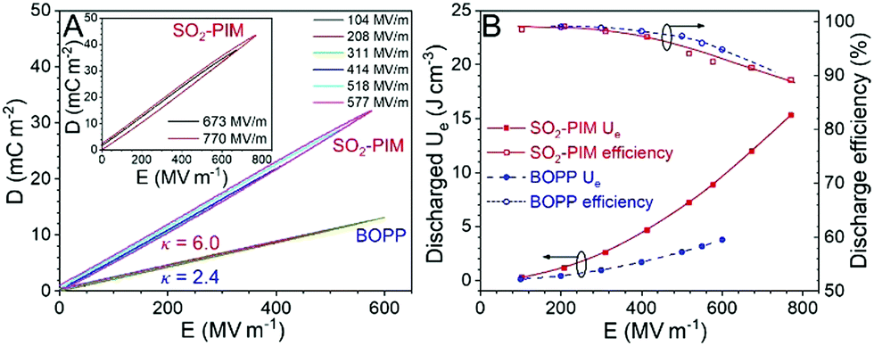 | ||
| Fig. 2 (A) Unipolar D–E loops for SO2-PIM under 1 kHz at room temperature. (B) Discharged energy density (Ue) and discharge efficiencies as a function of the poling field for SO2-PIM. BOPP is used for comparison. | ||
Compared with the state-of-the-art BOPP film, the discharge efficiency was similar; however, the discharged Ue of SO2-PIM was about 2.5 times that of BOPP. When the poling field increased to above 500 MV m−1, dielectric loss became more pronounced (Fig. 2A), which could be attributed to enhanced electronic conduction under high electric fields.38 However, the discharge efficiency was still ≥90% (Fig. 2B). When the poling field reached 770 MV m−1, a high discharged Ue of 17 J cm−3 was achieved.
Similar to other reports,36 no glass transition was found for SO2-PIM before the onset of thermal degradation (i.e., 360 °C with 1 wt% weight loss). The exceptionally high Tg of PIMs is desired for high-temperature dielectric applications. Fig. 3A shows high temperature bipolar D–E loops for the SO2-PIM film polarized at 300 MV m−1 (1 kHz). Below 150 °C, slim loops were observed. Fig. 3B presents the discharged Ue and discharge efficiency for SO2-PIM as a function of temperature, and the recently reported SO2-PPO25 was used for comparison.35 At 100 °C, SO2-PPO25 exhibited a higher discharged Ue than SO2-PIM because of its higher κ of 6.2. However, SO2-PIM had a higher discharge efficiency (94.4%) than that of SO2-PPO25 (91%). Upon increasing the temperature to 150 °C, the discharged Ue of SO2-PIM remained nearly constant and the discharge efficiency only slightly decreased to 93%. However, both the discharged Ue and discharge efficiency of SO2-PPO25 significantly decreased upon increasing the temperature to 150 °C. This was explained by enhanced charge injection from electrodes and thus high electronic conduction at elevated temperatures.35 Considering similar dielectric constants, it should be the higher Tg and suppressed space charge injection from metal electrodes for SO2-PIM to exhibit a lower dielectric loss than SO2-PPO25. Even at 175 °C, the SO2-PIM film still exhibited a reasonable discharge efficiency of 86%. When the poling field decreased to 200 MV m−1, high discharge efficiencies were still observed, i.e., 94% at 175 °C and 88% at 200 °C (Fig. 3C). These high temperature discharge efficiencies were comparable to a crossliniked divinyltetramethyldisiloxanebis(benzocyclo-butene)/boron nitride nanosheet (c-BCB/BNNS) composite reported recently.39 However, the discharged Ue of SO2-PIM was about twice that of c-BCB/BNNS because of its higher dielectric constant, i.e., 6.0 for SO2-PIM vs. 3.1 for c-BCB/BNNS.
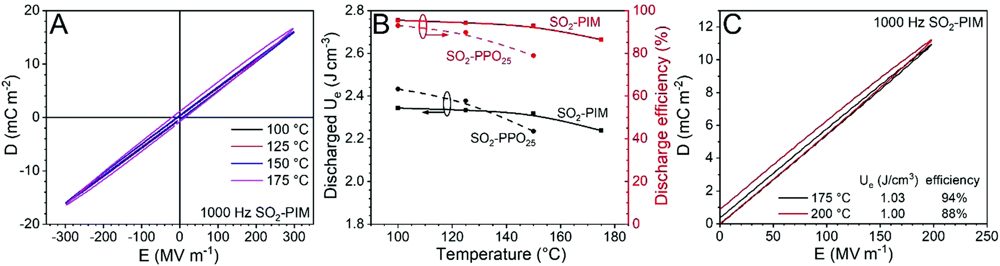 | ||
| Fig. 3 (A) Bipolar D–E loops at high temperatures for SO2-PIM. (B) Tempearture-dependent discharged energy density (Ue) and discharge efficiency for SO2-PIM and SO2-PPO under 300 MV m−1. (C) Unipolar D–E loops under 200 MV m−1 for SO2-PIM at 175 and 200 °C, respectively. | ||
Finally, the SO2-PIM was applied as a high-κ gate dielectric for InSe-based FETs. InSe is a 2D semiconductor with high electron mobility as well as strong spin–orbit coupling and has drawn a lot of attention in the past few years for the fabrication of high performance 2D semiconductor FETs or transport devices.40–42 As shown in Fig. 4A, an InSe nanoflake (∼20 nm thick) was exfoliated onto a Si/SiO2 substrate coated with SO2-PIM where both the silicon oxide (300 nm) and SO2-PIM (300–800 nm) were used as the gate dielectric. Electron beam evaporation was used to deposit a 5 nm layer of Ti followed by a 40 nm layer of Ni to form the source and drain electrodes contacting the InSe nanoflake on the SO2-PIM layer. The degenerately doped n-type Si substrate was used as the back-gate electrode. The InSe channel length was about 20 μm. To ensure good insulation, the leakage current density (J) was tested for a solution-cast SO2-PIM thin film capacitor (205 nm) at different temperatures. As seen in Fig. 4B, low J values of 8.8 × 10⁻¹³ A cm−2 at 3 V and 1.4 × 10⁻¹⁰ A cm−2 at 15 V were observed for SO2-PIM at room temperature. At 100 °C, the insulating property of SO2-PIM was still preserved with a relativley low J value of 1.9 × 10⁻⁹ A cm−2 at 6 V.
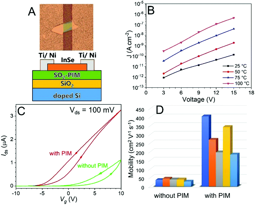 | ||
| Fig. 4 (A) Schematic of the InSe-based FET device and the top-view optical microscopy image. (B) Leakage current density as a function of voltage in a capacitor device. (C) The Ids–Vg transfer curve and (D) comparison of electron mobility in InSe for the FET devices with and without SO2-PIM. Five devices were tested for each type of FET. | ||
Typical Ids–Vg transfer curves are shown in Fig. 4C for the FET devices with and without SO2-PIM. The electron's field effect mobility could be calculated from the linear region of the transfer curves. Note that the hysteresis in the transfer curves could be attributed to certain surface defects on the dielectric layer that allowed certain charge injection.43 All FET devices with SO2-PIM exhibited a high electron mobility between 180 and 400 cm2 V−1 s−1, about 10× higher than those for the FET devices without SO2-PIM (Fig. 4D). The enhancement of mobility could be attributed to the screening effect from high-κ polar polymers.40,44 Namely, the SO2-PIM layer was used for screening interfacial Coulomb impurities, such as hydroxyl groups, moisture, and other chemical absorptions, resulting in improved charge carrier mobility and better performance of InSe FETs. Furthermore, Ids–Vg transfer curves in the logarithmic scale and Ids–Vds curves are shown in Fig. S7 (ESI†), demonstrating more clearly the ON–OFF switching of the device and ohmic behavior of the contacts. It can be seen in Fig. S7 (ESI†) that there was an indication of improved ON–OFF ratio with the presence of the SO2-PIM dielectric in the InSe FET, and the ON–OFF ratio reached at least 104 with the SO2-PIM gate dielectric (the actual ON–OFF ratio should be higher than 104 shown in Fig. S7 (ESI†), since the true OFF state was not reached in the measurement due to the limited sensitivity of the instrument). Combining relatively high dielectric constant, low dielectric loss, low leakage, and high-temperature tolerance, dipolar SO2-PIM is promising as a polymer gate dielectric for high-performance FETs.
In summary, utilizing highly polarizable sulfonyl groups, we introduced a new class of high-κ (5.3–6.0), high temperature (up to 200 °C), and low loss (tanδ ∼ 0.005) dielectric, SO2-PIM. The large pores (0.5–1.25 nm) were beneficial for the friction-free rotation of sulfonyl side groups. The highly rigid polymer structure with a high Tg prevented the backbone motions, resulting in low leakage current, high breakdown strength, and low dielectric loss at high temperatures. At room temperature, the discharged Ue reached 17 J cm−3 at 770 MV m−1. When it was used as a high-κ gate dielectric in the InSe FET device, a high electron mobility of 180–400 cm2 V−1 s−1 was achieved. These experimental results demonstrated exciting prospects for the polar PIMs to be used as high-performance dielectrics in printed electronics.
Conflicts of interest
The authors declare no competing financial interests.Acknowledgements
This work is supported by the National Science Foundation, Division of Materials Research, Polymers (DMR-1708990) and Condensed Matter Physics (DMR-1607631) Programs. This research used the 11-BM CMS beamline of National Synchrotron Light Source-II, Brookhaven National Laboratory (BNL), a U.S. Department of Energy User Facility operated for the Office of Science under contract No. DE-SC0012704.References
- L. Zhu, J. Phys. Chem. Lett., 2014, 5, 3677–3687 CrossRef CAS.
- Prateek, V. K. Thakur and R. K. Gupta, Chem. Rev., 2016, 116, 4260–4317 CrossRef CAS.
- E. Baer and L. Zhu, Macromolecules, 2017, 50, 2239–2256 CrossRef CAS.
- G. Wang, N. Persson, P. H. Chu, N. Kleinhenz, B. Y. Fu, M. Chang, N. Deb, Y. M. Mao, H. Z. Wang, M. A. Grover and E. Reichmanis, ACS Nano, 2015, 9, 8220–8230 CrossRef CAS.
- G. Wang, W. Huang, N. D. Eastham, S. Fabiano, E. F. Manley, L. Zeng, B. H. Wang, X. A. Zhang, Z. H. Chen, R. Li, R. P. H. Chang, L. X. Chen, M. J. Bedzyk, F. S. Melkonyan, A. Facchetti and T. J. Marks, Proc. Natl. Acad. Sci. U. S. A., 2017, 114, E10066–E10073 CrossRef CAS.
- Y. Khan, A. E. Ostfeld, C. M. Lochner, A. Pierre and A. C. Arias, Adv. Mater., 2016, 28, 4373–4395 CrossRef CAS.
- S. T. Han, Y. Zhou and V. A. L. Roy, Adv. Mater., 2013, 25, 5425–5449 CrossRef CAS.
- F. Carpi, D. De Rossi, R. Kornbluh, R. E. Pelrine and P. Sommer-Larsen, Dielectric Elastomers as Electromechanical Transducers: Fundamentals, Materials, Devices, Models and Applications of an Emerging Electroactive Polymer Technology, Elsevier, Oxford, UK, 2008 Search PubMed.
- A. Facchetti, M. H. Yoon and T. J. Marks, Adv. Mater., 2005, 17, 1705–1725 CrossRef CAS.
- Y. G. Ha, K. Everaerts, M. C. Hersam and T. J. Marks, Acc. Chem. Res., 2014, 47, 1019–1028 CrossRef CAS.
- R. P. Ortiz, A. Facchetti and T. J. Marks, Chem. Rev., 2010, 110, 205–239 CrossRef CAS PubMed.
- Y. H. Chou, H. C. Chang, C. L. Liu and W. C. Chen, Polym. Chem., 2015, 6, 341–352 RSC.
- S. A. DiBenedetto, A. Facchetti, M. A. Ratner and T. J. Marks, Adv. Mater., 2009, 21, 1407–1433 CrossRef CAS.
- A. A. Demkov and A. Navrotsky, Materials Fundamentals of Gate Dielectrics, Springer, Dordrecht, Netherland, 2005 Search PubMed.
- A. Gupta, P. Fang, M. Song, M. R. Lin, D. Wollesen, K. Chen and C. M. Hu, IEEE Electron Device Lett., 1997, 18, 580–582 CAS.
- Q. Chen, Y. Shen, S. Zhang and Q. M. Zhang, Annu. Rev. Mater. Res., 2015, 45, 433–458 CrossRef CAS.
- C. Vericat, M. E. Vela, G. Benitez, P. Carro and R. C. Salvarezza, Chem. Soc. Rev., 2010, 39, 1805–1834 RSC.
- R. L. McCreery and A. J. Bergren, Adv. Mater., 2009, 21, 4303–4322 CrossRef CAS.
- L. Yang, X. Li, E. Allahyarov, P. L. Taylor, Q. M. Zhang and L. Zhu, Polymer, 2013, 54, 1709–1728 CrossRef CAS.
- J. H. Li, Z. H. Sun and F. Yan, Adv. Mater., 2012, 24, 88–93 CrossRef CAS.
- X. Chen, L. Liu, S. Z. Liu, Y. S. Cui, X. Z. Chen, H. X. Ge and Q. D. Shen, Appl. Phys. Lett., 2013, 102, 063103 CrossRef.
- J. O. M. Bockris, A. K. N. Reddy and M. Gamboa-Aldeco, Modern Electrochemistry 2A, Kluwer Academic Publishers, New York, 2nd edn, ch. 6, 2000 Search PubMed.
- S. H. Kim, K. Hong, W. Xie, K. H. Lee, S. Zhang, T. P. Lodge and C. D. Frisbie, Adv. Mater., 2013, 25, 1822–1846 CrossRef CAS.
- J. R. Fried, in Physical Properties of Polymers Handbook, ed. J. E. Mark, Springer, New York, 2007 Search PubMed.
- R. H. M. Vandeleur, Polymer, 1994, 35, 2691–2700 CrossRef CAS.
- B. A. Bedekar, Y. Tsujii, N. Ide, Y. Kita, T. Fukuda and T. Miyamoto, Polymer, 1995, 36, 4735–4740 CrossRef CAS.
- T. Sato, Y. Tsujii, Y. Kita, T. Fukuda and T. Miyamoto, Macromolecules, 1991, 24, 4691–4697 CrossRef CAS.
- S. Tasaka, N. Inagaki, S. Miyata and T. Chiba, Sen’i Gakkaishi, 1988, 44, 546–550 CrossRef CAS.
- J. Y. Kim, H. Kim, T. Kim, S. Yu, J. W. Suk, T. Jeong, S. Song, M. J. Bae, I. Han, D. Jung and S. H. Park, J. Mater. Chem. C, 2013, 1, 5078–5083 RSC.
- T. Zhang, M. H. Litt and C. E. Rogers, J. Polym. Sci., Part A: Polym. Chem., 1994, 32, 2809–2816 CrossRef CAS.
- T. Zhang, M. H. Litt and C. E. Rogers, J. Polym. Sci., Part A: Polym. Chem., 1994, 32, 2291–2300 CrossRef CAS.
- J. Wei, Z. Zhang, J.-K. Tseng, I. Treufeld, X. Liu, M. H. Litt and L. Zhu, ACS Appl. Mater. Interfaces, 2015, 7, 5248–5257 CrossRef CAS.
- Y. X. Wang, X. Y. Huang, T. Li, Z. W. Wang, L. Q. Li, X. J. Guo and P. K. Jiang, J. Mater. Chem. A, 2017, 5, 20737–20746 RSC.
- Y.-F. Zhu, Z. Zhang, M. H. Litt and L. Zhu, Macromolecules, 2018, 51, 6257–6266 CrossRef CAS.
- Z. Zhang, D. H. Wang, M. H. Litt, L.-S. Tan and L. Zhu, Angew. Chem., Int. Ed., 2018, 57, 1528–1531 CrossRef CAS PubMed.
- N. Du, G. P. Robertson, I. Pinnau and M. D. Guiver, Macromolecules, 2009, 42, 6023–6030 CrossRef CAS.
- Z. Zhang, M. H. Litt and L. Zhu, Macromolecules, 2018, 51, 1967–1977 CrossRef CAS.
- S. Wu, W. Li, M. Lin, Q. Burlingame, Q. Chen, A. Payzant, K. Xiao and Q. M. Zhang, Adv. Mater., 2013, 25, 1734–1738 CrossRef CAS.
- Q. Li, L. Chen, M. R. Gadinski, S. Zhang, G. Zhang, H. U. Li, E. Iagodkine, A. Haque, L.-Q. Chen, T. N. Jackson and Q. Wang, Nature, 2015, 523, 576–579 CrossRef CAS.
- S. Sucharitakul, N. J. Goble, U. R. Kumar, R. Sankar, Z. A. Bogorad, F. C. Chou, Y. T. Chen and X. P. A. Gao, Nano Lett., 2015, 15, 3815–3819 CrossRef CAS.
- K. Premasiri, S. K. Radha, S. Sucharitakul, U. R. Kumar, R. Sankar, F. C. Chou, Y. T. Chen and X. P. A. Gao, Nano Lett., 2018, 18, 4403–4408 CrossRef CAS.
- D. A. Bandurin, A. V. Tyurnina, G. L. Yu, A. Mishchenko, V. Zólyomi, S. V. Morozov, R. K. Kumar, R. V. Gorbachev, Z. R. Kudrynskyi, S. Pezzini, Z. D. Kovalyuk, U. Zeitler, K. S. Novoselov, A. Patanè, L. Eaves, I. V. Grigorieva, V. I. Falko, A. K. Geim and Y. Cao, Nat. Nanotechnol., 2016, 12, 223–227 CrossRef.
- H. Wang, Y. Wu, C. Cong, J. Shang and T. Yu, ACS Nano, 2010, 12, 7221–7228 CrossRef.
- W. Feng, W. Zheng, W. Cao and P. Hu, Adv. Mater., 2014, 26, 6587–6593 CrossRef CAS.
Footnotes |
| † Electronic supplementary information (ESI) available. See DOI: 10.1039/c9mh01261c |
| ‡ These authors contributed equally to this work and should be considered as co-first authors. |
| This journal is © The Royal Society of Chemistry 2020 |