
 Open Access Article
 This Open Access Article is licensed under a
 Creative Commons Attribution 3.0 Unported Licence
The role of traps in the photocurrent generation mechanism in thin InSe photodetectors†
Qinghua
Zhao
abc,
Wei
Wang
ab,
Felix
Carrascoso-Plana
c,
Wanqi
Jie
ab,
Tao
Wang
 *ab,
Andres
Castellanos-Gomez
*c and
Riccardo
Frisenda
*c
*ab,
Andres
Castellanos-Gomez
*c and
Riccardo
Frisenda
*c
aState Key Laboratory of Solidification Processing, Northwestern Polytechnical University, Xi’an, 710072, P. R. China. E-mail: taowang@nwpu.edu.cn
bKey Laboratory of Radiation Detection Materials and Devices, Ministry of Industry and Information Technology, Xi’an, 710072, P. R. China
cMaterials Science Factory. Instituto de Ciencia de Materiales de Madrid (ICMM-CSIC), Madrid, E-28049, Spain. E-mail: andres.castellanos@csic.es; riccardo.frisenda@csic.es
First published on 11th September 2019
Abstract
Due to the excellent electrical transport properties and optoelectronic performance, thin indium selenide (InSe) has recently attracted attention in the field of 2D semiconducting materials. However, the mechanism behind the photocurrent generation in thin InSe photodetectors remains elusive. Here, we present a set of experiments aimed at explaining the strong scattering in the photoresponsivity values reported in the literature for thin InSe photodetectors. By performing optoelectronic measurements on thin InSe-based photodetectors operated under different environmental conditions we find that the photoresponsivity, the response time and the photocurrent power dependency are strongly correlated in this material. This observation indicates that the photogating effect plays an imporant role in thin InSe flakes, and it is the dominant mechanism in the ultra-high photoresponsivity of pristine InSe devices. In addition, when exposing the pristine InSe photodetectors to the ambient environment we observe a fast and irreversible change in the photoresponse, with a decrease in the photoresponsivity accompanied by an increase of the operating speed. We attribute this photodetector performance change (upon atmospheric exposure) to the decrease in the density of the traps present in InSe, due to the passivation of selenium vacancies by atmospheric oxygen species. This passivation is accompanied by a downward shift of the InSe Fermi level and by a decrease of the Fermi level pinning, which leads to an increase of the Schottky barrier between Au and InSe. Our study reveals the important role of traps induced by defects in tailoring the properties of devices based on 2D materials and offers a controllable route to design and functionalize thin InSe photodetectors to realize devices with either ultrahigh photoresposivity or fast operation speed.
New conceptsDefect related functionalization of semiconductors is a very important route to optimize the material properties and device performance. Unfortunately, in nanomaterials and in particular in 2D materials, the traditional bulk semiconductor defect engineering/doping methods (like annealing) usually cannot be directly transferred. In the post-growth stage, gas molecular doping is a popular way to tune the properties in 2D semiconductors. The presence of defects, such as chalcogen atom vacancies in chalcogen-based 2D semiconductors, offers a complementary platform to realize the functionalization of these 2D materials and tune their optoelectronic properties. In our manuscript we demonstrate that the interaction with oxygen species present in air can cure electronically active defects in InSe, a novel and promising 2D semiconductor, and tune the performances of photodetecting devices based on this material from high responsive configurations to fast responding ones. Both the intrinsic material doping and the metal electrode-2D semiconductor interface modification can be realized by the healing of chalcogen vacancies in air. This work demonstrates new horizons in the field of gas molecular-2D semiconductor interaction, which provides an efficient way to tailor the optoelectronic properties of InSe-based devices. |
Introduction
The isolation of ultrathin two-dimensional (2D) semiconducting materials, such as single-layer transition metal dichalcogenides (TMDCs) and few-layer black phosphorous (bP), has attracted large attention due to their potential applications in next-generation electronic and optoelectronic devices.1–5 The large surface-to-volume ratio of these 2D materials, which on one side makes them very tunable and sensitive to external stimuli, on the other side can make these materials and the devices based on them extremely vulnerable to environmental degradation.6–12 For example, when few-layer bP is exposed to the air, a fast degradation of the material occurs through a photooxidation process that leads to a reduction of the performances and the eventual failure of devices based on bP.6–8 A similar environmental degradation phenomenon has also been observed on thin gallium selenide (GaSe),9 gallium telluride (GaTe),13 and even CVD (chemical vapor deposition)-grown single-layer MoS2 and WS2, two members of the TMDC family.14 Moreover, the mobility of 2D semiconducting transistors kept in a vacuum or encapsulated with boron nitride is typically more than one order of magnitude larger than the mobility measured in the air.15,16 In the case of single-layer and bilayer MoS2, among the various reports, the device mobility at room temperature ranges from 0.1 cm2 V−1 s−1 in air to tens of cm2 V−1 s−1 in a vacuum or with top/bottom deposited protection materials.17–19 All these observations can be explained by the presence of defects in the materials, such as chalcogen vacancies in the layered metal chalcogenides.20–22 These defects can act as preferential sites for physical/chemical adsorption of environmental species (that can initiate the degradation process of 2D materials) and/or may introduce additional scattering of the carriers (that could act as harmful active traps in working devices).Indium selenide (InSe), an n-type semiconductor which belongs to the IIIVIA family, has recently attracted large attention because of its extraordinary charge transport properties, superior mechanical flexibility and strong light–matter interaction.23–41 Various groups have reported transistors based on thin InSe fabricated on different substrates (SiO2/Si, hexagonal Boron Nitride (h-BN), poly(methyl methacrylate) (PMMA)) with mobility values as large as 3700 cm2 V−1 s−1 at room temperature and ∼13![[thin space (1/6-em)]](https://www.rsc.org/images/entities/char_2009.gif) 000 cm2 V−1 s−1 at 4 K.23,25–28 The bandgap of 1.3 eV in bulk that becomes larger than 3 eV for an InSe single-layer makes this material interesting for broadband photodetection from the near-infrared to the near ultraviolet region of the electromagnetic spectrum.30–40
000 cm2 V−1 s−1 at 4 K.23,25–28 The bandgap of 1.3 eV in bulk that becomes larger than 3 eV for an InSe single-layer makes this material interesting for broadband photodetection from the near-infrared to the near ultraviolet region of the electromagnetic spectrum.30–40
Various photodetectors based on thin InSe flakes (as the active channel part), including metal–semiconductor–metal (M–S–M) geometry and graphene based van der Waals heterostructures, have been reported in the literature with responsivities going from 0.035 A W−1 to ultrahigh values of ∼107 A W−1 and detectivities up to ∼1015 Jones30–33,35–38,42 which are among the best performances reported for 2D photodetectors.33,40 See the ESI,† Table S1, for a comparison between the reported values in the literature for the figures of merit of InSe photodetectors. Such a large scattering in the responsivity values has also been observed for other chalcogenide-based 2D materials. For example in MoS2 photodetectors, traps states due to sulfur atomic vacancies influence the photocurrent generation giving rise to photogain and introducing Fermi level pinning at the metal–semiconductor (M–S) interface.43–49 Similarly, in the case of InSe, the defects related to In adatoms and Se vacancies, which can be related to the In-rich atmosphere in which high-quality InSe crytals are grown,50,51 may play important roles during the photocurrent generation process in thin InSe photodetectors.20,50–52 Interestingly, the presence of defects in InSe crystals, especially selenium vacancies (VSe),22 is predicted to promote the physical adsorption and chemical dissociation of O2/H2O molecules and VSe can act as preferential sites for the adsorption of these molecules.20,52–55 This phenomenon can help in explaining the performance degradation reported in various studies on thin InSe devices.20,33,51,54,56 Recently, both theoretical calculations and experimental scanning transmission electron microscopy (STEM) reported that the selenium vacancies VSe in InSe crystals can be passivated by chemical dissociation of O atoms at these sites.20,22,51 Similarly, Po-Hsun et al. demonstrated that the change of Raman and X-ray photoelectron spectra (XPS) of pristine InSe flakes exposed to ambient air is comparable to that observed when exposing InSe to dry oxygen atmosphere. The authors attribute these observations to the formation of a surficial InSe1−xOx layer that encapsulates the InSe beneath and promotes a long-term stability of thin InSe devices.26 Despite the large amount of work on InSe photodetectors, an important question that remains unanswered is how this passivation influences the optoelectronic properties of photodetectors based on thin InSe.
In this work, by comparing optoelectronic measurements obtained in InSe photodetectors operated under various environmental conditions, we propose a model to explain the photocurrent generation mechanism in InSe devices and how it is influenced by the environment. According to our observations, the optoelectronic properties of thin InSe photodetectors are stable over a long time of more than a few weeks when the devices are stored under vacuum conditions. When exposing the devices to ambient conditions, we observe a fast decrease of the responsivity accompanied by an increase in the operation speed (reduction of the response time) of the device. The high photoresponsivity observed in pristine thin InSe photodetectors can be attributed to a strong photogating (PG) effect, which mainly originates from traps for the minority carriers (holes). After exposing the device to the air, the passivation of the chalcogen vacancies VSe by oxygen induces a decrease in photocurrent, which can be explained by a decrease in the number of traps and a quenching of photogain and photogating in the system. Decreasing the density of traps in the 2D material has also a secondary effect on the devices; by reducing the Fermi level pinning we observe an increase of the Schottky barrier at the metal–semiconductor (M–S) interface consistent with the Schottky–Mott rule, as confirmed by scanning photocurrent measurements. Our results provide a further understanding of the photocurrent generation mechanism in photodetectors based on thin InSe and can pave the way to utilizing this novel material in high-performance electronics and optoelectronics.
Results and discussion
Thin InSe photodetectors are fabricated by deterministic placement of InSe flakes (thicknesses going from ∼5 nm to ∼20 nm) mechanically exfoliated from an InSe bulk crystal grown by the Bridgman method.57 By characterizing the InSe crystal with transmission electronic microscopy (TEM) and Raman spectroscopy, we find that the phase of the crystal is ε-type and that the estimated ratio between In and Se atoms is In:Se 1:0.993, see Fig. S1 of the ESI† and our previous work.36Fig. 1a shows the crystal structure of ε-InSe, with depicted two layers bound together by van der Waals forces. To isolate thin flakes of InSe, we first cleave larger flakes of the bulk InSe crystal onto Nitto tape (SPV 224) and then we transfer some of the flakes onto the surface of a polydimethylsiloxane (PDMS) stamp (Gel-Film by Gel-Pak) by gently pressing the tape against the stamp and peeling off slowly. The flakes on the PDMS can be then quickly transferred onto another arbitrary substrate with micrometric spatial precision by using a deterministic transfer setup.58,59Fig. 1b shows a microscopic picture of a thin InSe flake isolated onto PDMS (left) and a picture of the final photo-detecting device (right), formed by the same flake after being transferred bridging two pre-patterned electrodes (5 nm thick chromium sticking layer and 50 nm thick gold) evaporated on a SiO2/Si substrate (with a SiO2 thickness of 280 nm). To carry out the optoelectronic measurements the two gold electrodes (used a source and drain) are connected to a sourcemeter (Keithley® 2450) and the silicon substrate (heavily p-doped) is connected to a voltage source and used as a back gate. The differently colored regions of InSe deposited onto PDMS visible in Fig. 1b are due to different thicknesses of the material. From atomic force microscopy (AFM) topography measurements, we find that the thinnest region of the flake, which forms the channel in the final device, is 9.1 nm thick corresponding to approximately 11 layers.23
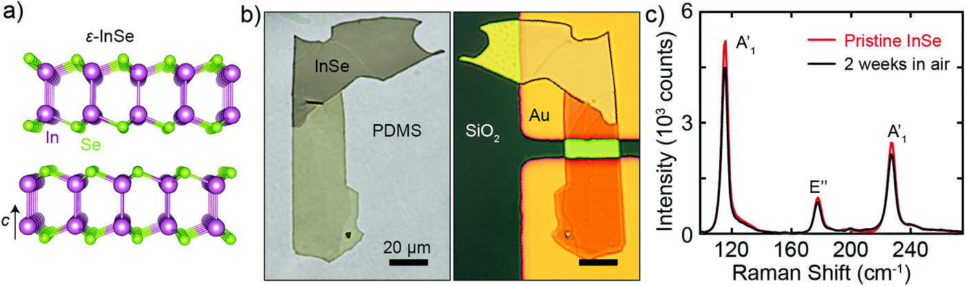 | ||
| Fig. 1 Layered semiconducting ε-InSe. (a) Crystal structure of InSe. (b) Optical pictures of few-layer InSe exfoliated onto PDMS (left) and deterministically transferred onto pre-patterned gold electrodes (right). (c) Raman spectra (532 nm laser, power density 0.11 mW μm−2) of the InSe flake shown in panel b recorded in the pristine state and after two weeks in air conditions. | ||
Just after the fabrication of the device, we performed Raman spectroscopy measurements of the InSe flake. Fig. 1c shows the Raman spectrum acquired on the region of the flake located above the gold electrode (indicated in Fig. 1b). The spectrum shows three prominent peaks centered at 116 cm−1, 178 cm−1, and 227 cm−1. These three peaks are due to vibrational modes of InSe and they can be attributed respectively to A1′, E′′ and A1′. A fourth peak is visible at 200 cm−1 and is due to A2′′ (see Fig. S1b, ESI†), which is sensitive to the crystalline phase.36 Since the degradation of 2D materials is a common phenomenon, we test the stability of the InSe flake by repeating the Raman measurements after two weeks of exposure to ambient conditions. As can be seen from Fig. 1c and Fig. S2 (ESI†) the Raman spectra of the pristine flake and the one of the aged flake are very similar, the only difference being a ∼15% reduction of the intensity of the peaks in the aged spectrum (see Fig. S3, ESI† for similar results obtained on additional flakes). This observation is consistent with previous Raman and XPS studies from the literature (see the ESI of ref. 39 and 26, 28, 34).26,28,34,39,60 We estimate that the reduction of the Raman signal corresponds to the degradation of the top ∼1–2 layers. Therefore, these Raman measurements indicate that the structure of mechanically exfoliated thin InSe flakes does not degrade completely upon exposure to ambient air, a different behavior from thin black phosporous or GaSe.6,9
To investigate the properties of pristine InSe photodetectors, we perform optoelectronic measurements on a freshly prepared device kept in a vacuum (sample #1 in Fig. S4, ESI†). We carried out the measurements in a home-made vacuum probe-station connected to a turbomolecular pumping station capable of reaching a base vacuum level of ∼1 × 10⁻⁶ mbar. All the measurements presented in this article were performed at room temperature (T = 300 K). Fig. 2a shows the transfer curve of the device, that is the source-drain current recorded while slowly changing the gate voltage VG. This measurement was performed with a bias voltage VDS of 1 V and keeping the device under dark conditions. The device shows negligible current at negative gate voltages (off state, VG < VT) and starts to conduct current for positive voltages (on state, VG > VT). These observations indicate that the InSe channel is n-doped and from the plot we extract a threshold voltage VT = 10 V, which is in agreement with previous reports on InSe transistors.23,25–28 From this transfer curve we can also estimate the electron mobility using the equation:
 | (1) |
 | (2) |
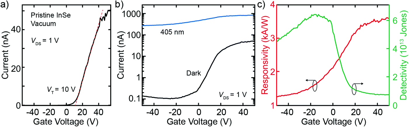 | ||
| Fig. 2 Optoelectronic characterization of a pristine InSe photodetector (#1) in a vacuum. (a) Current versus back gate voltage transfer curve at VSD = 1 V of a pristine InSe photodetector kept in a vacuum and in the dark. (b) Current versus gate voltage in dark and under illumination at 405 nm (power density 0.92 W m−2) represented in a semi-logarithmic scale. (c) Responsivity (R, left axis) and detectivity (D*, right axis) of pristine InSe extracted from the curves in panel (b). | ||
After the characterization of the InSe photodetector under dark conditions, we test its optoelectronic properties and response to external illumination. The blue curve in Fig. 2b corresponds to the transfer curve of the device under external illumination with a light source of wavelength 405 nm and power density of 10−4 W cm−2. Under these conditions, the current passing through the device increases to a maximum of 1000 nA in the on state and to more than 200 nA in the off state, corresponding to an increase from the dark current of more than one order of magnitude in the on case and of three orders of magnitude in the off state. From the current measured while keeping the device in the dark (Idark) and under external illumination (Ilight), we can calculate the responsivity R and the detectivity D* of the photodetector using the following equations:62,63
| R = |Iph|/(PA), | (3) |
| D* = RA1/2/(2eIdark)1/2, | (4) |
In the following, we focus on the influence of air on the performances of InSe photodetectors. Just after the device fabrication, a pristine InSe photodetector (sample #2 in Fig. S4, ESI†) was stored in a high vacuum (pressure ∼10−6 mbar) and the optoelectronic performance was measured. To characterize the device in this case we studied its response in time to external square-wave modulated illumination. The red curve in Fig. 3a shows the current flowing in the device at VDS = 1 V as a function of time (I–t) while switching on and off a 530 nm light source focused onto the surface of the device. The two curves of Fig. 3a have been recorded with two illumination power densities, 450 mW μm−2 and 225 mW μm−2. When switching on the illumination at around 30 s with power 450 mW μm−2 the current starts to slowly increase from ∼400 pA to ∼43 nA in approximately 100 s giving a responsivity of 0.09 A W−1, while in the case of 225 mW μm−2 the current reaches a value of ∼25 nA and the responsivity is 0.11 A W−1. This increase of the responsivity for decreasing illumination power densities points to the presence of traps for minority carriers (holes) in the device and we will discuss in more detail the power dependent measurements later in the article.46,47
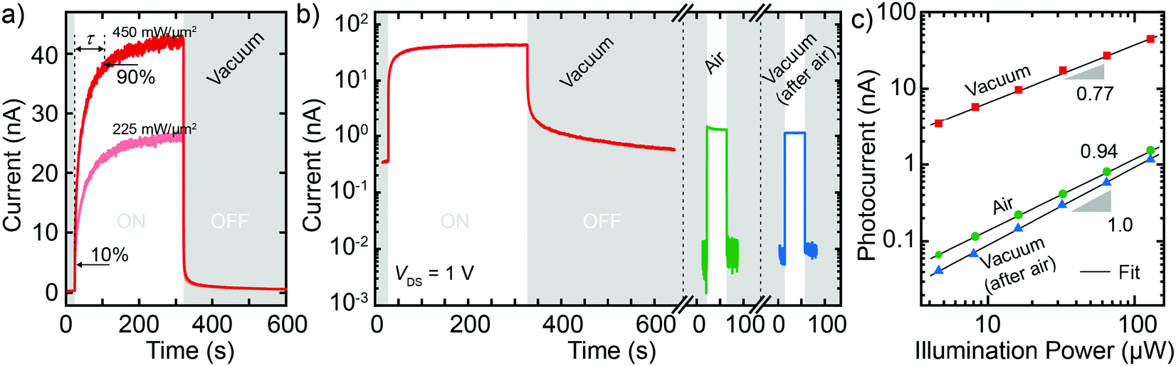 | ||
| Fig. 3 Evolution in the air of an InSe photodetector (#2). (a) Current at VSD = 1 V recorded in an InSe photodetector as a function of time while turning on and off a 530 nm light source with two different illumination powers. (b) Current at VSD = 1 V recorded in an InSe photodetector as a function of time while turning on and off illumination at 530 nm (power density 450 mW μm−2). The device was kept first in a vacuum (pressure ∼10−6 mbar), then it was transferred into the air for ∼20 hours (∼103 mbar) and finally it was kept again in a vacuum. (c) Photocurrent as a function of illumination power at 530 nm recorded in the three environments of panel (b). | ||
The slow response of the photocurrent to external illumination shown in Fig. 3a can be quantitatively characterized by the response time, which we estimate using the 10%–90% criterion. Here the response time is defined as the time that it takes for the current to increase from 10% of the saturation value to 90%. From the current vs. time traces (I–t) at 450 mW μm−2 we estimate a rising time τon = 77 s and a decay time τoff = 3.2 s (see Section 4 of the ESI† for a discussion about the difference in rising and decay time based on Shockley and Read statistics64). Fig. 3b shows the data just discussed plotted in semi-logarithmic scale, where the small dark current of ∼400 pA is visible. After carrying out the measurements in a vacuum we exposed the device to air under ambient conditions for approximately 20 hours and then we repeated the I–t measurements. The green curve in Fig. 3b is the corresponding I–t measured in air with the same illumination parameters used for the I–t in a vacuum. As can be seen from the plot, both the dark current Idark and the current under illumination Ilight recorded in air conditions are much smaller than the initial values recorded in a vacuum and the photocurrent Iph becomes ∼1.2 nA, a ∼40 times reduction. At the same time, we also observe a decrease of both the rising and decay time of the device, which becomes smaller than ∼60 ms, approximately 2 or 3 orders of magnitude smaller than the initial values. Subsequently, after measuring the device in the air, we evacuated the chamber reaching again a pressure of ∼10−6 mbar and we carried out the same optoelectronic characterization. From the blue curve shown in Fig. 3b, one can see that both Idark and Ilight remain at the same level recorded in the air indicating that the device underwent an irreversible transformation after being exposed to air for ∼20 hours. The extracted responsivity is 0.002 A W−1 and both the rising and the decay time are equal to ∼40 ms. From these measurements, we find that by exposing the device to air, the InSe photodetector goes from an initial state with larger responsivity but slower time response to a final state with smaller responsivity and faster time response.
In a photodetector, important information about the mechanism behind the photocurrent generation can be extracted from the power dependency of the photocurrent.9,65 During the I–t measurements discussed above, we also measured the photocurrent for different light intensities going from 45 mW μm−2 to 450 mW μm−2. For each value of light intensity, we extract the maximum photocurrent and we plot the results in Fig. 3c. The photocurrent as a function of the illumination power density is shown in a log–log representation and the three datasets correspond to the three states of the device (1 pristine in a vacuum, 2 after 20 hours of exposure to air, 3 in a vacuum after being exposed to air). From the graph, one can see that each of the three datasets follows approximately a straight line, indicating that the photocurrent and the illumination power are connected by a power law. This relation can be expressed by the equation:
| Iph = b·Pα, | (5) |
The increase of α in InSe photodetectors exposed to air, discussed above for a single device, has been observed in all the five investigated Au–InSe–Au devices (see Fig. S6 of the ESI†). Moreover, a similar increase in α has been observed also in graphite–InSe–graphite devices (see the ESI† Fig. S9). Importantly, this common behavior is independent of the initial parameters of the measured devices such as responsivity, α or response time. This fact has been illustrated in Fig. 4a and b where we collect the results of five different devices (shown in Fig. S4, ESI†) measured in the pristine state and after several exposure times to air. Fig. 4a shows a semi-logarithmic graph of the decay time of the five devices plotted as a function of the exponent α, extracted from power-dependent I–t measurements similar to the ones shown in Fig. 3a. The different devices are represented by data-points with different shapes and colors. As can be seen from the statistical plot, among all the investigated InSe photodetectors the exponent α can take values between ∼0.3 and 1 and correspondingly, the decay time goes from thousands of seconds when α is smaller than 0.5 (photogating dominated devices) to values smaller than 0.1 s (a value that could be limited by the experimental resolution of 0.04 s) when α tends to 1 (purely photoconductive (PC) devices). The plot shows a clear dependency of the decay time on the power exponent α for all the InSe photodetectors and indicates that the two variables are inversely proportional. A second statistical correlation can be observed between the responsivity R and the decay time τoff as shown in Fig. 4b. In this log–log plot, the decay time of the five different InSe photodetectors is plotted versus the photoresponsivity extracted for each device. In this case, we measured responsivity values going from 10−3 A W−1 to 102 A W−1 corresponding to decay times going from less than 0.1 s to more than 1000 s. The graph shows a correlation between the two with the data-points following approximately a straight line, which indicates that the two variables are connected by a power law. The black dashed line represents a power law with an exponent equal to 1, corresponding to a linear relationship between the responsivity and the response time. As can be seen from the plot, for large values of both R and τoff, the data-points follow perfectly the linear relation, suggesting that the photogating effect is the dominant mechanism for InSe photodetectors with large responsivities. In fact, in photogating dominated devices the minority carriers get trapped in long-lived charge traps which limits in an effective way the response time of the device (they are typically slower than photoconductive devices) but provides an external source of photogain (when the channel drift time of the charge carriers is much shorter than the charge trapping time the device presents a photogain proportional to τoff/τdrift).43,46 For lower values of R and τoff, the data-points start to deviate from the linear relation and present larger scattering, which could be due to the photocurrent generation mechanism being less dominated by photogating. In fact, while in the PG regime R and τoff are dependent variables (linked through the carrier drift time), in the PC regime the responsivity is limited to a finite value according to:
| R = η·λ/1240, | (6) |
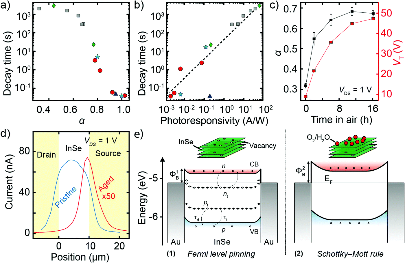 | ||
| Fig. 4 Photocurrent generation mechanism in the InSe photodetectors. (a) Decay time as a function of the exponent α of the photocurrent-power scaling law extracted from all the investigated InSe photoetectors. (b) The relationship between decay time and photoresponsivity in various InSe photdetectors. All the dots in the same shape and color were measured with the same device after different air exposure times. (c) Photocurrent exponent α (left axis) and threshold voltage VT (right axis) recorded in a device (#1) exposed to air as a function of time. (d) Spatially resolved photocurrent at Vds = 1 V of device #4 recorded just after fabrication (blue) and after 10 days in air (red). (e) Schematic band diagram of InSe under dark conditions with traps and Fermi level pinning (1, left) and in the absence of traps with the alignment predicted by the Schottky–Mott rule (2, right). Depicted there are the valence (VB) and conduction band (CB) of InSe, the gold elecrodes and the Fermi energy (EF) and a set of hole trapping levels (whose density is Pt) and electron trapping level (density Nt). The density of free electrons, free holes, trapped electrons and trapped holes are respectively n, p, nt. and pt. | ||
After exploring the correlation between α, R and τoff we discuss a last set of experiments that highlight the change in the electronic structure of InSe after the exposure to air. After the initial optoelectronic characterization of device #1 in a vacuum (transfer curves and photocurrent power dependency at 405 nm, see Fig. S5 in the ESI†), we expose the device to air in a dark environment for 2 hours and then we evacuate again the vacuum chamber and perform the optoelectronic measurements. We repeat these measurements during air-vacuum cycles until the performances of the InSe photodetector become stable (approximately after 16 hours of air exposure). In Fig. 4c we plot both the exponent α (left axis), extracted from the power dependency of the photocurrent, and the threshold voltage VT (right axis), extracted from the transfer curves, both plotted as a function of the exposure time to the air. As can be seen, the exponent α increases from 0.32 to 0.67, indicating the reduction in the trap state density and the change in the photocurrent generation mechanism from PG (α = 0.32) to PC (α = 0.67). At the same time VT (recorded under dark conditions) increases from ∼10 V to ∼50 V, a clear sign of the incremental p-doping of the InSe channel.26,34 The evolution of the transfer curves of this device and additional measurements under illumination can be found in Fig. S7 of the ESI.† In a second experiment, we study the evolution of the spatially resolved photocurrent in device #4 using scanning photocurrent microscopy. Briefly, in this technique we focus a 650 nm laser in a ∼1 μm2 circular spot onto the surface of the InSe photodetector and move it across the sample while recording for each position the source-drain current and the intensity of the reflected light (see Fig. S10 of the ESI†). Fig. 4d shows the average current recorded in device #4 while scanning the laser spot from the source to the drain electrode in steps of 0.5 μm under pristine conditions (blue curves) and after 10 days of exposure to air (red). The line-profile of the pristine device at VDS = 1 V shows a broad and high photocurrent intensity region over the entire InSe channel area. In contrast, the aged device presents a strong and sharp photocurrent peak located near the source contact at the end of the device channel, which is consistent with the presence of Schottky barriers at the InSe/gold contacts.66,67 See Fig. S10 of the ESI† for the measurements under applied bias of VSD = −1 V.
Before discussing a model that can explain the photocurrent generation mechanism in thin InSe photodetectors it is instructive to summarize the experimental observations presented above. In summary, we studied five different InSe photodetectors in their freshly fabricated pristine state, and after the exposure to ambient conditions.
1. From electrical measurements in a field effect transistor configuration, we find that pristine InSe photodetectors are n-type doped (Fig. 2a).
2. The optoelectronic figures-of-merit of pristine InSe photodetectors are excellent, with responsivities of the order of 103 A W−1 and detectivities of ∼1013 Jones. The responsivity depends on the gate voltage, decreasing when the InSe photodetectors are operated in the off state (Fig. 2b and c).
3. From time-resolved measurements we find that the time response in pristine InSe photodetectors is slow and can be on the order of thousands of seconds (Fig. 3a and b).
4. After exposing the InSe photodetectors to the air we observe a decrease of both the dark current and the current under illumination, accompanied by a decrease in response time (Fig. 3b). Statistically, the responsivity and the response time across all the investigated photodetector are strongly correlated (Fig. 4b).
5. The exposure to the air also affects the way in which the photocurrent depends on the illumination power density. While pristine InSe photodetectors show a sublinear dependency of Iph on P, with the power law exponent α taking a value lower than 1, the exposure to air increases the linearity of this relation, with the power law exponent α increasing toward 1 (Fig. 3c).
6. Scanning photocurrent measurements (Fig. 4d) show that the interface between gold and pristine InSe shows lower Schottky barriers than that of aged InSe.
The n-type doping observed in the transfer curves of pristine thin InSe photodetectors measured in the dark and under vacuum conditions has been observed in different experiments apart from the ones presented in this article.23,25–28 This behavior can be attributed to the presence of defects in the crystal such as selenium vacancies and indium interstial adatoms (IIn) that can be caused by the In-rich atmosphere in which high-quality InSe is grown.50,51 These intrinsic defects are expected to modify the density of states of InSe and theoretical calculations predict the appearance of trap states linked to these defects. While VSe can introduce two sets of trap levels, the first one is located closer to the conduction band minimun (CBM) and the second is closer to the valence band maximum (VBM), the trap levels due to IIn are located only closer to CBM.51,52 In Fig. 4e we show a schematic band diagram of the system composed by InSe, with the conduction band CB and the valence band VB displayed, and two gold electrodes acting as electron reservoirs. The Fermi energy of the electrodes EF is closer to CB in agreement with the n-type conduction observed in the experiments. The majority carrier trap levels, which are closer to the conduction band, have a density Nt and can act as pinning centers for the Fermi level of the device at zero bias. On the other hand, the minority carrier traps with density Pt are expected to play a dominant role in the photocurrent generation process since they can generate photogain.20,51,52,55 Under dark conditions the InSe channel has a density of free electrons n (located in CB) and of free holes p (VB) and, as a consequence of the position of the Fermi level, there is a small density of trapped holes pt (meaning that most of the trap levels are occupied by electrons, density nt). A free hole in VB (free electron in CB) has a certain probability of getting trapped by a trap level with rate τt−1. The opposite process also is possible and a trapped hole (electron) can jump from a trap level to VB (CB) with rate τd−1. In general, the trapping and detrapping rates τt−1 and τd−1 can be different and there can be also a difference between the rates relative to holes and electrons.
The band diagram of Fig. 4e can be used to explain the current flowing through the device under dark conditions and serves as a basis to understand the photogeneration of current. When we illuminate the InSe photodetectors with external illumination, electron–hole pairs are generated and the density of free holes p and free electrons n increases. The separation of these electron–hole pairs due to the electric field related to the source-drain voltage gives rise to a photocurrent. This process is usually called the “photoconducting effect” and does not show photogain. In fact, the maximum responsivity achievable in a photodetector working solely by PC for illumination can be calculated through eqn (6) and in the case of illumination at 405 nm the maximum responsivity is ∼0.33 A W−1. In the absence of active traps in the photodetector, PC is typically the dominant photocurrent generation mechanism. On the other hand, if hole traping levels are present in the system, each photogenerated hole has a certain probability (related to τt−1) of getting trapped in one of these levels for an average time τd. This trapping process for minority carriers can give rise to a “photogating effect” (PG), a process that can show photogain and can give responsivities much larger than ∼0.33 A W−1 at 405 nm. The magnitude of the photogain is related to the ratio between the trapping time and the drift time (the trapping time can be many orders of magnitude larger than the drift time).43,46 In the case of a pristine InSe photodetector measured in a vacuum (stage 1), the large responsivity values can be explained by PG. This mechanism also explains the large response times recorded for pristine photodetectors as in the PG mechanism the reponse speed is limited by the trapping time. The power dependency of the photocurrent also confirms this scenario. In fact, a photodetector without trap levels is expected to be characterized by a value of the exponent α equal to 1 while in a photodetector containing active traps, α is smaller than 1. For the pristine InSe devices, dominated by the PG effect, the interface between gold and InSe is characterized by small Schottky barriers, consistent with the scanning photocurrent measurements of device #4, and the alignment between the Fermi level of InSe and of the gold electrodes is determined by the Fermi level pinning to the trap levels.49,68
The right panel of Fig. 4e, schematises the evolution in the band structure after the exposure of InSe photodetectors to air (stage 2). In this case, we propose that a change in the trap levels induces a strong change in the photocurrent generation process. In fact, the interaction between the selenium vacancies and the oxygen or water molecules present in air leads to a passivation of the defects, as predicted by theoretical calculations,20,51,55 thus reducing the trap densities Nt and Pt (in our simplified scheme we removed completely the traps). The passivation process will eventually stop after all the avalaible vacancy sites are neutralized, characterized by a trap density much smaller than the initial density Pt at stage 1. At this stage of the evolution fewer holes can be trapped, effectively decreasing the photogain. The photodetector working principle shifts from PG to PC and the power dependency of the photocurrent illustrates well this evolution, with the aged InSe photodetectors showing a linear dependency of the photocurrent on the incident power. Once the InSe photodetectors reach this stage of evolution (stage 2), they become much faster in responding to light (as the trapping time does not limit the photodetector speed anymore) but at the expense of a reduced responsivity. In this limit, the interface between gold and InSe is characterized by larger Schottky barriers and the alignment between InSe and gold can be calculated by the Schottky–Mott rule,69,70 which predicts that the Schottky barrier formed at the interface has the value ΦSB,n = WM − XS ∼ 0.5 eV, where WM is the work function of gold (∼5.1 eV) and XS is the electron affinity of InSe (∼4.6 eV). The Schottky barriers are visible in Fig. 4d in the line-profile of the aged InSe photodetector.66,67 Importantly, the final state of the photodetector seems to be stable both in the air and in a vacuum suggesting that the passivation is a self-limiting process.20 A final feature of the model, is the change of the relative alignment of the Fermi energy with respect to CB and VB during the evolution of InSe. In fact, the reduction of the density of trap levels is expected to induce a shift of the Fermi energy away from the conduction band, effectively introducing p-doping in the InSe channel.52,53 The consequences of the p-doping can be observed in the reduction of the dark current in the air compared to the pristine one as shown in Fig. 3b and in the shift of the threshold voltage.
Conclusions
In conclusion, by investigating the photocurrent generation process in InSe and its evolution in air/vacuum we find that traps levels can induce a strong photogain effect in pristine InSe photodetectors. The healing of these traps after exposure of InSe to air reduces the photogain and increases the operation speed of the photodetecting devices. The statistical analyses based on all our investigated thin InSe devices suggest that photoresponsivity, response time and the photocurrent scaling law exponent α are all strongly correlated quantities. The proposed band diagram model indicates that the high photoresponsivity in pristine thin InSe photodetectors can be attributed to the photogating effect, which mainly originates from the hole-trapping levels induced by selenium vacancies. The air-induced passivation of defects may reduce the traps density in thin InSe photodetectors, thus shifting the photocurrent generation mechanism from photogating to photoconductive. This change is accompanied by a decrease in photoresponse time and photoresponsivity as well as the growth of exponent α. This work illustrates the strong effect of intrinsic defects, present in pristine 2D semiconductors, on their optoelectronic properties and how a controlled healing of these defects can be a powerful route to continuously tune the performance of these devices in a broad range of operational conditions.Materials and methods
Sample fabrication
Thin InSe flakes were fabricated using a mechanical exfoliation method with scotch tape and Nitto tape (Nitto Denko® SPV 224) and then transferred onto a polydimethylsiloxane substrate (PDMS). After inspection with optical microscopy transmission mode (Motic® BA310 MET-T), the selected flakes were transferred from the PDMS to the pre-patterned Au (50 nm)/SiO2 (280 nm)/Si substrates (Osilla®) to fabricate the photodetector devices.58,59 All the channel lengths of the InSe photodetectors are 10 μm.Raman spectroscopy
The Raman spectra of thin InSe flakes were obtained by a Bruker Senterra confocal Raman microscopy setup (Bruker Optik®, Ettlingen, Germany) with a laser excitation of 0.2 mW at 532 nm focused in a 1 μm diameter spot. The integration time is 20 s.Optoelectronic characterization
Thin InSe photodetectors are characterized in a homebuilt high-vacuum (∼1 × 10⁻⁶ mbar, room temperature T = 300 K) chamber. The electrical measurements (I–V, I–t) were performed with a source-meter source-measure unit (Keithley® 2450). The light source is provided by light emitting diodes (LEDD1B – T-Cube LED driver, Thorlabs®) with wavelength from 405 nm to 850 nm, coupled to a multimode optical fiber at the LED source and projected onto the sample surface by a zoom lens, creating a light spot on the sample with the diameter of 600 μm. The spatially resolved photocurrent maps under various source-drain voltage biases (−0.1 V, 0 V and 0.1 V) are acquired with a home-made scanning photocurrent system based on a modified microscope (BA310Met-H Trinocular, MOTIC) and a motorized XY scanning stage (8MTF, Standa).71AFM measurements
The thickness of thin InSe flakes was measured by an ezAFM (by Nanomagnetics) atomic force microscope operated in dynamic mode. The cantilever used is a Tap190Al-G by BudgetSensors with force constant 40 Nm-1 and resonance frequency 300 kHz.Conflicts of interest
The authors declare no competing financial interests.Acknowledgements
This project has received funding from the European Research Council (ERC) under the European Union's Horizon 2020 research and innovation programme (grant agreement no 755655, ERC-StG 2017 project 2D-TOPSENSE). EU Graphene Flagship funding (Grant Graphene Core 2, 785219) is acknowledged. RF acknowledges support from the Netherlands Organization for Scientific Research (NWO) through the research program Rubicon with project number 680-50-1515 and from the Spanish Ministry of Economy, Industry and Competitiveness through a Juan de la Cierva-formación fellowship (2017 FJCI-2017-32919). QHZ acknowledges the grant from China Scholarship Council (CSC) under No. 201700290035. TW acknowledges support from the National Natural Science Foundation of China: 51672216.References
- Q. H. Wang, K. Kalantar-Zadeh, A. Kis, J. N. Coleman and M. S. Strano, Electronics and optoelectronics of two-dimensional transition metal dichalcogenides, Nat. Nanotechnol., 2012, 7, 699–712 CrossRef CAS.
- K. F. Mak and J. Shan, Photonics and optoelectronics of 2D semiconductor transition metal dichalcogenides, Nat. Photonics, 2016, 10, 216 CrossRef CAS.
- L. Li, Y. Yu, G. J. Ye, Q. Ge, X. Ou, H. Wu, D. Feng, X. H. Chen and Y. Zhang, Black phosphorus field-effect transistors, Nat. Nanotechnol., 2014, 9, 372 CrossRef CAS.
- A. Castellanos-Gomez, L. Vicarelli, E. Prada, J. O. Island, K. Narasimha-Acharya, S. I. Blanter, D. J. Groenendijk, M. Buscema, G. A. Steele and J. Alvarez, Isolation and characterization of few-layer black phosphorus, 2D Mater., 2014, 1, 025001 CrossRef.
- A. Castellanos-Gomez, Why all the fuss about 2D semiconductors?, Nat. Photonics, 2016, 10, 202–204 CrossRef CAS.
- J. O. Island, G. A. Steele, H. S. van der Zant and A. Castellanos-Gomez, Environmental instability of few-layer black phosphorus, 2D Mater., 2015, 2, 011002 CrossRef.
- A. Favron, E. Gaufrès, F. Fossard, A.-L. Phaneuf-L’Heureux, N. Y. Tang, P. L. Lévesque, A. Loiseau, R. Leonelli, S. Francoeur and R. Martel, Photooxidation and quantum confinement effects in exfoliated black phosphorus, Nat. Mater., 2015, 14, 826–832 CrossRef CAS PubMed.
- J. D. Wood, S. A. Wells, D. Jariwala, K.-S. Chen, E. Cho, V. K. Sangwan, X. Liu, L. J. Lauhon, T. J. Marks and M. C. Hersam, Effective passivation of exfoliated black phosphorus transistors against ambient degradation, Nano Lett., 2014, 14, 6964–6970 CrossRef CAS PubMed.
- Q. Zhao, R. Frisenda, P. Gant, D. Perez de Lara, C. Munuera, M. Garcia-Hernandez, Y. Niu, T. Wang, W. Jie and A. Castellanos-Gomez, Toward Air Stability of Thin GaSe Devices: Avoiding Environmental and Laser-Induced Degradation by Encapsulation, Adv. Funct. Mater., 2018, 28, 1805304 CrossRef.
- G. Wang, R. Pandey and S. P. Karna, Physics and chemistry of oxidation of two-dimensional nanomaterials by molecular oxygen, Wiley Interdiscip. Rev.: Comput. Mol. Sci., 2017, 7, e1280 Search PubMed.
- W. Cao, J. Jiang, X. Xie, A. Pal, J. H. Chu, J. Kang and K. Banerjee, 2-D Layered Materials for Next-Generation Electronics: Opportunities and Challenges, IEEE Trans. Electron Devices, 2018, 65, 4109–4121 CAS.
- Q. Li, Q. Zhou, L. Shi, Q. Chen and J. Wang, Recent advances in oxidation and degradation mechanisms of ultrathin 2D materials under ambient conditions and their passivation strategies, J. Mater. Chem. A, 2019, 7, 4291–4312 RSC.
- S. Yang, Y. Qin, B. Chen, V. O. Özçelik, C. E. White, Y. Shen, S. Yang and S. Tongay, Novel surface molecular functionalization route to enhance environmental stability of tellurium-containing 2D layers, ACS Appl. Mater. Interfaces, 2017, 9, 44625–44631 CrossRef CAS PubMed.
- J. Gao, B. Li, J. Tan, P. Chow, T.-M. Lu and N. Koratkar, Aging of transition metal dichalcogenide monolayers, ACS Nano, 2016, 10, 2628–2635 CrossRef CAS PubMed.
- H. Qiu, T. Xu, Z. Wang, W. Ren, H. Nan, Z. Ni, Q. Chen, S. Yuan, F. Miao and F. Song, Hopping transport through defect-induced localized states in molybdenum disulphide, Nat. Commun., 2013, 4, 2642 CrossRef PubMed.
- W. Park, J. Park, J. Jang, H. Lee, H. Jeong, K. Cho, S. Hong and T. Lee, Oxygen environmental and passivation effects on molybdenum disulfide field effect transistors, Nanotechnology, 2013, 24, 095202 CrossRef PubMed.
- B. Radisavljevic, A. Radenovic, J. Brivio, I. V. Giacometti and A. Kis, Single-layer MoS2 transistors, Nat. Nanotechnol., 2011, 6, 147 CrossRef CAS PubMed.
- M. S. Fuhrer and J. Hone, Measurement of mobility in dual-gated MoS2 transistors, Nat. Nanotechnol., 2013, 8, 146 CrossRef CAS.
- M. Chhowalla, D. Jena and H. Zhang, Two-dimensional semiconductors for transistors, Nat. Rev. Mater., 2016, 1, 16052 CrossRef CAS.
- Y. Liu, P. Stradins and S. H. Wei, Air Passivation of Chalcogen Vacancies in Two-Dimensional Semiconductors, Angew. Chem., 2016, 128, 977–980 CrossRef.
- W. Zhou, X. Zou, S. Najmaei, Z. Liu, Y. Shi, J. Kong, J. Lou, P. M. Ajayan, B. I. Yakobson and J.-C. Idrobo, Intrinsic structural defects in monolayer molybdenum disulfide, Nano Lett., 2013, 13, 2615–2622 CrossRef CAS PubMed.
- D. G. Hopkinson, V. Zólyomi, A. P. Rooney, N. Clark, D. J. Terry, M. Hamer, D. J. Lewis, C. S. Allen, A. I. Kirkland and Y. Andreev, Formation and Healing of Defects in Atomically Thin GaSe and InSe, ACS Nano, 2019, 13, 5112–5123 CrossRef CAS.
- D. A. Bandurin, A. V. Tyurnina, L. Y. Geliang, A. Mishchenko, V. Zólyomi, S. V. Morozov, R. K. Kumar, R. V. Gorbachev, Z. R. Kudrynskyi and S. Pezzini, High electron mobility, quantum Hall effect and anomalous optical response in atomically thin InSe, Nat. Nanotechnol., 2017, 12, 223 CrossRef CAS.
- G. W. Mudd, S. A. Svatek, T. Ren, A. Patanè, O. Makarovsky, L. Eaves, P. H. Beton, Z. D. Kovalyuk, G. V. Lashkarev and Z. R. Kudrynskyi, Tuning the bandgap of exfoliated InSe nanosheets by quantum confinement, Adv. Mater., 2013, 25, 5714–5718 CrossRef CAS.
- M. Li, C. Y. Lin, S. H. Yang, Y. M. Chang, J. K. Chang, F. S. Yang, C. Zhong, W. B. Jian, C. H. Lien and C. H. Ho, High Mobilities in Layered InSe Transistors with Indium-Encapsulation-Induced Surface Charge Doping, Adv. Mater., 2018, 1803690 CrossRef.
- P.-H. Ho, Y.-R. Chang, Y.-C. Chu, M.-K. Li, C.-A. Tsai, W.-H. Wang, C.-H. Ho, C.-W. Chen and P.-W. Chiu, High-mobility InSe transistors: the role of surface oxides, ACS Nano, 2017, 11, 7362–7370 CrossRef CAS.
- S. Sucharitakul, N. J. Goble, U. R. Kumar, R. Sankar, Z. A. Bogorad, F.-C. Chou, Y.-T. Chen and X. P. Gao, Intrinsic electron mobility exceeding 103 cm2 (V s)−1 in multilayer InSe FETs, Nano Lett., 2015, 15, 3815–3819 CrossRef CAS PubMed.
- Y.-T. Huang, Y.-H. Chen, Y.-J. Ho, S.-W. Huang, Y.-R. Chang, K. Watanabe, T. Taniguchi, H.-C. Chiu, C.-T. Liang and R. Sankar, High-Performance InSe Transistors with Ohmic Contact Enabled by Nonrectifying Barrier-Type Indium Electrodes, ACS Appl. Mater. Interfaces, 2018, 10, 33450–33456 CrossRef CAS.
- X. Liu, J.-C. Ren, S. Zhang, M. Fuentes-Cabrera, S. Li and W. Liu, Ultrahigh Conductivity in Two-Dimensional InSe via Remote Doping at Room Temperature, J. Phys. Chem. Lett., 2018, 9, 3897–3903 CrossRef CAS.
- S. Lei, F. Wen, L. Ge, S. Najmaei, A. George, Y. Gong, W. Gao, Z. Jin, B. Li and J. Lou, An atomically layered InSe avalanche photodetector, Nano Lett., 2015, 15, 3048–3055 CrossRef CAS.
- S. Lei, L. Ge, S. Najmaei, A. George, R. Kappera, J. Lou, M. Chhowalla, H. Yamaguchi, G. Gupta and R. Vajtai, Evolution of the electronic band structure and efficient photo-detection in atomic layers of InSe, ACS Nano, 2014, 8, 1263–1272 CrossRef CAS.
- S. R. Tamalampudi, Y.-Y. Lu, U. R. Kumar, R. Sankar, C.-D. Liao, B. K. Moorthy, C.-H. Cheng, F. C. Chou and Y.-T. Chen, High performance and bendable few-layered InSe photodetectors with broad spectral response, Nano Lett., 2014, 14, 2800–2806 CrossRef CAS PubMed.
- S. A. Wells, A. Henning, J. T. Gish, V. K. Sangwan, L. J. Lauhon and M. C. Hersam, Suppressing Ambient Degradation of Exfoliated InSe Nanosheet Devices via Seeded Atomic Layer Deposition Encapsulation, Nano Lett., 2018, 18, 7876–7882 CrossRef CAS.
- Y.-R. Chang, P.-H. Ho, C.-Y. Wen, T.-P. Chen, S.-S. Li, J.-Y. Wang, M.-K. Li, C.-A. Tsai, R. Sankar and W.-H. Wang, Surface oxidation doping to enhance photogenerated carrier separation efficiency for ultrahigh gain indium selenide photodetector, ACS Photonics, 2017, 4, 2930–2936 CrossRef CAS.
- W. Feng, J.-B. Wu, X. Li, W. Zheng, X. Zhou, K. Xiao, W. Cao, B. Yang, J.-C. Idrobo and L. Basile, Ultrahigh photo-responsivity and detectivity in multilayer InSe nanosheets phototransistors with broadband response, J. Mater. Chem. C, 2015, 3, 7022–7028 RSC.
- Z. Yang, W. Jie, C.-H. Mak, S. Lin, H. Lin, X. Yang, F. Yan, S. P. Lau and J. Hao, Wafer-scale synthesis of high-quality semiconducting two-dimensional layered InSe with broadband photoresponse, ACS Nano, 2017, 11, 4225–4236 CrossRef CAS.
- W. Luo, Y. Cao, P. Hu, K. Cai, Q. Feng, F. Yan, T. Yan, X. Zhang and K. Wang, Gate Tuning of High-Performance InSe-Based Photodetectors Using Graphene Electrodes, Adv. Opt. Mater., 2015, 3, 1418–1423 CrossRef CAS.
- G. W. Mudd, S. A. Svatek, L. Hague, O. Makarovsky, Z. R. Kudrynskyi, C. J. Mellor, P. H. Beton, L. Eaves, K. S. Novoselov and Z. D. Kovalyuk, High broad-band photoresponsivity of mechanically formed InSe–graphene van der Waals heterostructures, Adv. Mater., 2015, 27, 3760–3766 CrossRef CAS.
- Z. Chen, J. Biscaras and A. Shukla, A high performance graphene/few-layer InSe photo-detector, Nanoscale, 2015, 7, 5981–5986 RSC.
- J. Kang, S. A. Wells, V. K. Sangwan, D. Lam, X. Liu, J. Luxa, Z. Sofer and M. C. Hersam, Solution-Based Processing of Optoelectronically Active Indium Selenide, Adv. Mater., 2018, 30, 1802990 CrossRef.
- Q. Zhao, R. Frisenda, T. Wang and A. Castellanos-Gomez, InSe: a two-dimensional semiconductor with superior flexibility, Nanoscale, 2019, 11, 9845–9850 RSC.
- H.-W. Yang, H.-F. Hsieh, R.-S. Chen, C.-H. Ho, K.-Y. Lee and L.-C. Chao, Ultraefficient Ultraviolet and Visible Light Sensing and Ohmic Contacts in High-Mobility InSe Nanoflake Photodetectors Fabricated by the Focused Ion Beam Technique, ACS Appl. Mater. Interfaces, 2018, 10, 5740–5749 CrossRef CAS.
- M. M. Furchi, D. K. Polyushkin, A. Pospischil and T. Mueller, Mechanisms of photoconductivity in atomically thin MoS2, Nano Lett., 2014, 14, 6165–6170 CrossRef CAS PubMed.
- D.-S. Tsai, K.-K. Liu, D.-H. Lien, M.-L. Tsai, C.-F. Kang, C.-A. Lin, L.-J. Li and J.-H. He, Few-layer MoS2 with high broadband photogain and fast optical switching for use in harsh environments, ACS Nano, 2013, 7, 3905–3911 CrossRef CAS PubMed.
- W. Zhang, J. K. Huang, C. H. Chen, Y. H. Chang, Y. J. Cheng and L. J. Li, High-gain phototransistors based on a CVD MoS2 monolayer, Adv. Mater., 2013, 25, 3456–3461 CrossRef CAS PubMed.
- M. Buscema, J. O. Island, D. J. Groenendijk, S. I. Blanter, G. A. Steele, H. S. van der Zant and A. Castellanos-Gomez, Photocurrent generation with two-dimensional van der Waals semiconductors, Chem. Soc. Rev., 2015, 44, 3691–3718 RSC.
- N. Huo and G. Konstantatos, Recent Progress and Future Prospects of 2D-Based Photodetectors, Adv. Mater., 2018, 30, 1801164 CrossRef.
- C. Kim, I. Moon, D. Lee, M. S. Choi, F. Ahmed, S. Nam, Y. Cho, H.-J. Shin, S. Park and W. J. Yoo, Fermi level pinning at electrical metal contacts of monolayer molybdenum dichalcogenides, ACS Nano, 2017, 11, 1588–1596 CrossRef CAS.
- D. S. Schulman, A. J. Arnold and S. Das, Contact engineering for 2D materials and devices, Chem. Soc. Rev., 2018, 47, 3037–3058 RSC.
- H. Wang, J.-j. Shi, P. Huang, Y.-m. Ding, M. Wu, Y.-l. Cen and T. Yu, Origin of n-type conductivity in two-dimensional InSe: In atoms from surface adsorption and van der Waals gap, Phys. E, 2018, 98, 66–73 CrossRef CAS.
- K. Xiao, A. Carvalho and A. C. Neto, Defects and oxidation resilience in InSe, Phys. Rev. B, 2017, 96, 054112 CrossRef.
- A. A. Kistanov, Y. Cai, K. Zhou, S. V. Dmitriev and Y.-W. Zhang, Atomic-scale mechanisms of defect-and light-induced oxidation and degradation of InSe, J. Mater. Chem. C, 2018, 6, 518–525 RSC.
- A. Politano, G. Chiarello, R. Samnakay, G. Liu, B. Gürbulak, S. Duman, A. Balandin and D. Boukhvalov, The influence of chemical reactivity of surface defects on ambient-stable InSe-based nanodevices, Nanoscale, 2016, 8, 8474–8479 RSC.
- L. Shi, Q. Zhou, Y. Zhao, Y. Ouyang, C. Ling, Q. Li and J. Wang, Oxidation mechanism and protection strategy of ultrathin Indium Selenide: Insight from Theory, J. Phys. Chem. Lett., 2017, 8, 4368–4373 CrossRef CAS PubMed.
- D. Ma, T. Li, D. Yuan, C. He, Z. Lu, Z. Lu, Z. Yang and Y. Wang, The role of the intrinsic Se and In vacancies in the interaction of O2 and H2O molecules with the InSe monolayer, Appl. Surf. Sci., 2018, 434, 215–227 CrossRef CAS.
- X. Wei, C. Dong, A. Xu, X. Li and D. D. Macdonald, Oxygen-induced degradation of the electronic properties of thin-layer InSe, Phys. Chem. Chem. Phys., 2018, 20, 2238–2250 RSC.
- T. Ishii, High quality single crystal growth of layered InSe semiconductor by Bridgman technique, J. Cryst. Growth, 1988, 89, 459–462 CrossRef CAS.
- A. Castellanos-Gomez, M. Buscema, R. Molenaar, V. Singh, L. Janssen, H. S. van der Zant and G. A. Steele, Deterministic transfer of two-dimensional materials by all-dry viscoelastic stamping. 2D, Materials, 2014, 1, 011002 Search PubMed.
- R. Frisenda, E. Navarro-Moratalla, P. Gant, D. P. De Lara, P. Jarillo-Herrero, R. V. Gorbachev and A. Castellanos-Gomez, Recent progress in the assembly of nanodevices and van der Waals heterostructures by deterministic placement of 2D materials, Chem. Soc. Rev., 2018, 47, 53–68 RSC.
- D. Pozo-Zamudio, S. Schwarz, J. Klein, R. Schofield, E. Chekhovich, O. Ceylan, E. Margapoti, A. Dmitriev, G. Lashkarev and D. Borisenko, Photoluminescence and Raman investigation of stability of InSe and GaSe thin films, 2015, arXiv preprint arXiv:1506.05619.
- A. Ayari, E. Cobas, O. Ogundadegbe and M. S. Fuhrer, Realization and electrical characterization of ultrathin crystals of layered transition-metal dichalcogenides, J. Appl. Phys., 2007, 101, 014507 CrossRef.
- W. Choi, M. Y. Cho, A. Konar, J. H. Lee, G. B. Cha, S. C. Hong, S. Kim, J. Kim, D. Jena and J. Joo, High-detectivity multilayer MoS2 phototransistors with spectral response from ultraviolet to infrared, Adv. Mater., 2012, 24, 5832–5836 CrossRef CAS.
- M. S. Choi, D. Qu, D. Lee, X. Liu, K. Watanabe, T. Taniguchi and W. J. Yoo, Lateral MoS2 p–n junction formed by chemical doping for use in high-performance optoelectronics, ACS Nano, 2014, 8, 9332–9340 CrossRef CAS.
- G. Taylor and J. Simmons, Basic equations for statistics, recombination processes, and photoconductivity in amorphous insulators and semiconductors, J. Non-Cryst. Solids, 1972, 8, 940–946 CrossRef.
- O. Lopez-Sanchez, D. Lembke, M. Kayci, A. Radenovic and A. Kis, Ultrasensitive photodetectors based on monolayer MoS 2, Nat. Nanotechnol., 2013, 8, 497 CrossRef CAS.
- H. Jin, J. Li, L. Wan, Y. Dai, Y. Wei and H. Guo, Ohmic contact in monolayer InSe-metal interface, 2D Mater., 2017, 4, 025116 CrossRef.
- B. Shi, Y. Wang, J. Li, X. Zhang, J. Yan, S. Liu, J. Yang, Y. Pan, H. Zhang and J. Yang, n-Type Ohmic contact and p-type Schottky contact of monolayer InSe transistors, Phys. Chem. Chem. Phys., 2018, 20, 24641–24651 RSC.
- C. H. Ho and Y. J. Chu, Bending photoluminescence and surface photovoltaic effect on multilayer InSe 2D microplate crystals, Adv. Opt. Mater., 2015, 3, 1750–1758 CrossRef CAS.
- Y. Liu, J. Guo, E. Zhu, L. Liao, S.-J. Lee, M. Ding, I. Shakir, V. Gambin, Y. Huang and X. Duan, Approaching the Schottky–Mott limit in van der Waals metal–semiconductor junctions, Nature, 2018, 557, 696 CrossRef CAS.
- S. M. Sze and K. K. Ng, Physics of semiconductor devices, John Wiley & Sons, 2006 Search PubMed.
- C. Reuter, R. Frisenda, D. Y. Lin, T. S. Ko, D. Perez de Lara and A. Castellanos-Gomez, A versatile scanning photocurrent mapping system to characterize optoelectronic devices based on 2D materials, Small Methods, 2017, 1, 1700119 CrossRef.
Footnote |
| † Electronic supplementary information (ESI) available. See DOI: 10.1039/c9mh01020c |
| This journal is © The Royal Society of Chemistry 2020 |