 Open Access Article
Creative Commons Attribution 3.0 Unported Licence
Selective deposition of silver and copper films by condensation coefficient modulation†
Silvia
Varagnolo
 a,
Jaemin
Lee
 a,
Houari
Amari‡
b and
Ross A.
Hatton
 *a
*a
aDepartment of Chemistry, University of Warwick, CV4 7AL, Coventry, UK. E-mail: Ross.Hatton@warwick.ac.uk
bDepartment of Physics, University of Warwick, CV4 7AL, Coventry, UK
First published on 13th August 2019
Abstract
Whilst copper and silver are the conductors of choice for myriad current and emerging applications, patterning these metals is a slow and costly process. We report the remarkable finding that an extremely thin (∼10 nm) printed layer of specific organofluorine compounds enables selective deposition of copper and silver vapour, with metal condensing only where the organofluorine layer is not. This unconventional approach is fast, inexpensive, avoids metal waste and the use of harmful chemical etchants, and leaves the metal surface uncontaminated. We have used this approach to fabricate thin films of these metals with 6 million apertures cm−2 and grids of ∼1 μm lines, through to 10 cm diameter apertures. We have also fabricated semi-transparent organic solar cells in which the top silver electrode is patterned with a dense array of 2 μm diameter apertures, which cannot be achieved by any other scalable means directly on an organic electronic device.
New conceptsHere we report the proof-of-principle of a new concept in the selective deposition of copper and silver electrodes that completely avoids metal waste and the use of harmful chemical etchants, and leaves the metal surface uncontaminated, the latter being particularly important for frontier applications in sensors and organic electronics. We show that both silver and copper vapour do not condense on extremely thin (∼10 nm) printed layers of specific organofluorine compounds, so the metal is deposited only where the organofluorine layer is not. The beauty of this approach lies in its versatility and accessibility, since vacuum evaporation of metals is proven as a low cost metal deposition method by the packaging industry, and the shape and dimensions of the features deposited is limited only by the printing method used to deposit the patterned organofluorine layer. Here we have used micro-contact printing to demonstrate proof-of-principle, although the approach is not limited to this printing method. We demonstrate the power of this approach by fabricating semi-transparent organic solar cells in which the top silver electrode is patterned with a 6 million 2 μm diameter apertures cm−2 which, to our knowledge, cannot be achieved by any other scalable means directly on an organic electronic device. |
Introduction
Silver (Ag) and copper (Cu) are the dominant current carrying elements in modern electronics and solar cells, and also the metals of choice for a diverse range of emerging applications including flexible transparent electrodes and as platforms for biological and chemical sensors for point-of-use healthcare and environmental monitoring.1–7 When structured on the sub-wavelength scale the unique optical properties of these metals also enables them to trap and channel visible light in the form of surface plasmonic excitations,8 rendering them ideal as active-elements for a plethora of future optoelectronic applications9 and as a platform for the nascent field of plasmonic nano-chemistry.6 For all of these applications these metals are patterned by printing from costly colloidal solutions of nanoparticles followed by sintering to fuse the nanoparticles together,10 or by selective removal of metal by etching using harmful chemicals,11 or by electrochemical deposition.12,13 Whilst the latter has the advantage that it enables selective metal deposition, it is an inherently chemical intensive and slow solution based process.12,13 Additionally, using all of these methods contamination of the metal surface by organic residues is inevitable, which modifies the work function in an uncontrolled way14 and impedes subsequent chemical derivatization of the surface, which is limiting for frontier applications in sensors and organic electronics.Vacuum evaporation is a proven low cost method for the large area deposition of metal films and so is widely used in the food packaging industry, as well as being ubiquitous in research laboratories. Due to the industrial importance of the metallisation of insulating substrates a great deal of effort has been directed at improving adhesion between evaporated metal films and glass and polymer substrates.15,16 Studies of the very early stage nucleation of Ag and Cu on plastics, equivalent to a metal thickness of 1–2 atoms,17,18 have shown that whilst all metal atoms are initially adsorbed at the surface not all remain, with the proportion remaining adsorbed quantified in terms of the sticking or condensation coefficient, C. Whilst a great deal of effort has been directed at maximising C, reports pertaining to how C can be intentionally minimised, or how substrates with very low C might be exploited for selective deposition of metals are sparse19–23 and the ‘Holy Grail’ of selective deposition of Ag and Cu has remained elusive until now. In addition to the obvious technological advantage for manufacturing industry, the emergence of an accessible method for the selective deposition of Ag and Cu opens the door to the accelerated research and development of single use, disposable devices that would otherwise be uneconomically viable due to the high cost of patterning films of these metals over macroscopic areas.
In this work we report an unconventional, inexpensive and highly effective approach to the selective deposition of Ag and Cu, based on the use of very small quantities of cheap, low toxicity organofluorine compounds in the form of printed thin films. We have identified that Ag and Cu vapours do not condense on thin films of highly fluorinated organic compounds, and demonstrate this for metal deposition equivalent to 85 nm – a thickness sufficient to completely block visible light. When Ag and Cu are evaporated onto printed organofluorine layers with a pattern, metal is only deposited where the organofluorine layer is not, ensuring that metal is deposited only where it is needed. Consequently, there is no metal removal step, which avoids metal waste and eliminates the adverse environmental impact associated with the use of chemical etchants, leaving a pristinely clean metal surface. The beauty of this method lies in its simplicity, since vacuum evaporation of metals is a widely available technique and the shape and dimensions of the features deposited is only limited by the printing method used. The generality of this approach is demonstrated using both polymeric and small molecule fluorinated compounds and by applying this approach to glass, plastic and silicon substrates for both Ag and Cu. The versatility is demonstrated by fabrication of metal films with features on the micron scale through to a tenth of a meter, and semi-transparent organic solar cells in which the top transparent silver electrode is patterned with a dense array of 2 μm diameter apertures per square cm.
Results & discussion
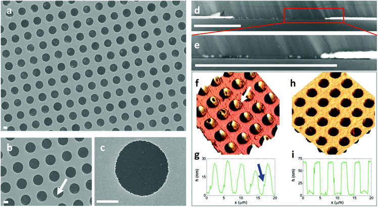
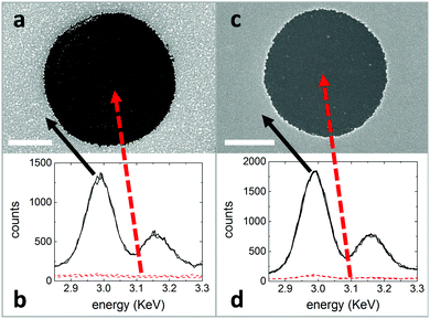
To demonstrate the power of this approach we have used micro-contact printing (μCP) to print arrays of 2.5 μm circles of (1H,1H,2H,2H-perfluorooctyl)trichlorosilane (FTS) (Table S1, ESI†) with a density of ∼ 6 million apertures cm−2 onto high C transparent substrates (Fig. 1 and Fig. S1, ESI†). μCP uses an elastomer stamp with elevated features that make intimate conformal contact with a substrate for the selective printing of thin films on surfaces, and can be scaled to large areas24 as well as being easily implementable on a laboratory scale.25 The widely available fluorinated molecule FTS is identified as offering an extremely low C for both Cu and Ag deposited by thermal evaporation and is amenable to μCP. The materials used to impart a high C to the different substrates used in this study were molybdenum oxide (MoO3−x) and polyethylenimine (PEI), which are deposited as very thin films by vacuum evaporation and from dilute solution respectively.Fig. 1 and ESI† Fig. S2–S5 show representative scanning electron microscope (SEM) and cross-sectional scanning transmission electron microscope (STEM) images of 15 nm, 50 nm and 85 nm thick Ag films thermally evaporated onto FTS printed films, from which it is evident that the metal selectively deposits only in those areas where the substrate is not covered with FTS. Spatially resolved energy dispersive X-ray spectroscopy (EDXS) spectra acquired on metallized and non-metallized areas for films with a nominal Ag thickness of 15 nm and 85 nm (Fig. 2) confirm this conclusion. Analysis of the cross-sectional STEM image (Fig. 1d and e) confirm that the thickness of the metallized areas is equal to that which condenses on the quartz crystal microbalance. When the deposited Ag thickness is increased to 85 nm (Fig. 1a–c, h, i, c, d and Fig. S6, ESI†), the apertures are still largely free of Ag, which demonstrates the broad range of metal thickness over which this approach is applicable.
Comparison of the STEM images for Ag films of 15 and 50 nm thickness (Fig. 1d, e and Fig. S2–S5, ESI†) reveal that there are a few isolated Ag nanoparticles in FTS printed regions which are larger when the metal thickness is increased. It is also clear from the STEM images that where isolated Ag nanoparticles are present in printed areas they are invariably located at the interface between the MoO3−x layer and the printed silane layer (Fig. 1d, e and Fig. S4, ESI†), which indicates that nucleation occurs where Ag can diffuse through the FTS layer reaching the underlying substrate. AFM images of the micro-contact printed substrates before metal deposition show that FTS printed regions have a mound shape with a central peak height of several tens of nanometres that tapers to zero thickness at the edges (Fig. 1f and g). Where Ag nanoparticles are present in FTS printed regions they are most prevalent at the edges of the circular apertures where the printed layer is thinnest (Fig. 1a, b and Fig. S6, ESI†). Additionally, a common artefact of the μCP process is a crescent shaped trench at the outer edge of the printed circular area, where the FTS is locally thinner (indicated with an arrow in Fig. 1f and g), which correlates with a crescent shaped distribution of Ag nanoparticles after metal deposition (Fig. 1b and Fig. S6, ESI†). Together these observations provide compelling evidence that Ag nanoparticles form where the FTS layer is thin enough for the Ag to diffuse through to the underlying substrate. Diffusion of metals into polymer substrates is well known,26–28 particularly during the initial stage of polymer metallization where the system is far from equilibrium, and is a consequence of the very weak intermolecular interactions and open surface structure of most polymer surfaces at the microscopic level.
To determine the minimum thickness of the FTS layer needed to achieve selective Ag deposition, glass derivatized with the monochlorosilane analogue of FTS, 1H,1H,2H,2H-perfluorooctyldimethylchlorosilane (FMS) was prepared (Table S1, ESI†). Since FMS has only one chlorosilane moiety polymerisation cannot occur and so the chemisorbed layer is limited to one monolayer, which is equivalent to ∼ 1 nm thickness. It is evident from Fig. S7 (ESI†) that a monolayer of FMS is not sufficient to block Ag deposition, because the sample is an intense dark green colour typical of a dense array for Ag particles. To test the generality of this finding a monolayer of the thiol analogue of FTS, tridecafluoro-1-octanethiol, was formed on an ultra-smooth semi-transparent Au film16 using a deposition method known to result in a compact thiol monolayer on Au.29 Again, it is clear from ESI† Fig. S8 that a monolayer was not sufficient to block Ag condensation. EDXS analysis shows that the amount of Ag deposited onto substrates derivatised with a monolayers of FMS and the thiol analogue is the same as on the substrates without a monolayer (Fig. S7 and S8, ESI†). Collectively these data are consistent with Ag atoms being initially adsorbed at the surface and diffusing sub-surface before either being ejected back into the vapour phase, or nucleating at the substrate surface. Whilst the extent of this sub-surface diffusion inevitably depends on the composition and structure of the printed film (the latter depending on the deposition method) and the metal deposition rate,30 we find that an FTS layer with a thickness of ≥10 nm is needed to achieve selective deposition: Fig. S9 and Table S2 (ESI†).
To demonstrate another deposition method for the FTS layer, 3.2 cm2 glass slides were coated with a 10–20 nm thick film of FTS deposited by spin coating, followed by evaporation of Ag equivalent to a nominal metal thickness of 15 nm. It is evident from the EDXS analysis (Fig. S10 and Table S3, ESI†) and from the photographs in Tables S1 and S2 (ESI†) that there is no significant metal deposition over the entire FTS coated slide. Conversely, Ag does deposit onto films of comparable thickness of the hydrocarbon analogue of FTS; octyltrichlorosilane (OTS) (Tables S1 and S2, ESI†), which shows that the fluorocarbon backbone is the essential feature of the molecule for selective deposition, rather than the silane moiety. This conclusion is confirmed by the demonstration of selective deposition using the polymeric organofluorine:poly(vinylidene fluoride-co-hexafluoropropylene) (PVDF-HFP), which has no silane functionality (Table S1, ESI†). To show that selective deposition can be achieved over large areas we have increased the circular aperture size from the micron-scale to a tenth of a metre (Fig. 3).
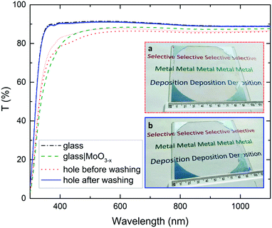
For specific applications it may be necessary to remove the printed organofluorine layer and metal nucleation layer from those areas not covered with metal in order to minimise unnecessary parasitic light absorption, as shown in Fig. 3 for a 10 cm diameter aperture in a 50 nm thick Ag film. It is evident from the transmittance spectra in Fig. 3 that in this case the MoO3−x metal nucleation layer contributes substantially to parasitic absorption for wavelengths below 450 nm. Due to the very low thickness of the organofluorine layer needed to achieve selective deposition, it is easily and quickly removed by rising with a solvent that dissolves it, or in the case of a cross-linked silane layer such as FTS, by rinsing using 0.2 M tetrabutylammonium fluoride/tetrahydrofuran solution, to realise arrays of apertures of well-defined depth (Fig. S11, ESI†). The MoO3−x metal nucleation layer can then be removed by briefly rinsing in water.
To deposit optically thin metal films with well-defined thickness we have used a relatively low metal deposition rate of ∼1 Angstrom per second. Increasing the deposition rate by a factor of 5–6 times (and the deposited metal thickness to 70 nm) resulted in more nanoparticle deposition, although only at the edges of the printed area: Fig. S12 (ESI†). Away from the edges, where the FTS layer is thicker, apertures are essentially free of metal. Increasing the metal deposition rate requires the temperature of the metal source to be raised, which increases the mean kinetic energy of the incident metal atoms. It is therefore reasonable to expect that the propensity of the metal atoms to diffuse into the printed layer will be higher when the metal deposition rate is increased. Consequently, to accommodate higher metal deposition rate the thickness of the printed organofluorine layer must be increased.
We have found that this approach to the selective deposition of Ag is also applicable to the lighter group 11 metal; Cu (Fig. S13, S14 and Table S3, ESI†). Cu does not bind strongly to MoO3−x and so forms isolated particles for a nominal metal thickness of 15 nm (Fig. S13a and b, ESI†). For this reason a solution processed PEI layer was used in place of MoO3−x to achieve compact Cu films on metallized areas (Fig. S13c–e, ESI†). This method can be translated to flexible transparent plastic polyethylene terephthalate (PET) substrates for both Cu and Ag, using MoO3−x as an adhesion layer for Ag and PEI for Cu (Fig. 4 and Fig. S13 and S15, ESI†).
Transparent flexible electrodes
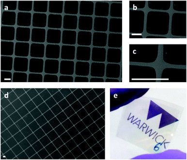
To demonstrate an important application, we have fabricated transparent electrodes on flexible substrates based on a grid of Ag lines ∼1 μm wide and 50 nm thick, suitable as transparent electrodes in flexible optoelectronics (Fig. 4d and e). In this case the grid spacing is 18.5 μm which corresponds to 10% metal coverage (Fig. 4d). These electrodes have an average absolute transparency across the wavelength range 400–1100 nm of ∼78% although 12% of the incident light is attenuated by the PET substrate and MoO3−x adhesion layer due to reflection and absorption (Fig. S16, ESI†). Of the light transmitted through the substrate, only 11% is attenuated by the metal grid, which correlates closely with the Ag metal coverage. Brief rinsing with tetrabutylammonium fluoride/tetrahydrofuran followed by water increases the absolute transparency to 80% due to the removal of the FTS and MoO3−x layer together with any Ag nanoparticles at defect sites in the FTS printed regions. The very small improvement in transparency, which is in large part due to removal of the MoO3−x adhesion layer, demonstrates the effectiveness of the selective deposition approach. In this case the sheet resistance of this electrode is ∼30 Ohm sq−1, although this can be reduced by increasing the thickness of the Ag grid lines without increasing the area of the electrode obscured by the metal.Top-electrode for semi-transparent organic solar cells
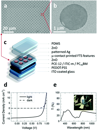
To further demonstrate the power of this approach for applications, we have fabricated semi-transparent organic photovoltaic devices in which the top Ag electrode has a dense array of ∼2 μm diameter apertures (Fig. 5) fabricated using the aforementioned method. To our knowledge there is no other scalable means of realising a metal electrode patterned with this density of features directly on top of an organic optoelectronic device.Conclusions
The power of the approach reported herein for the fabrication of patterned Ag and Cu films lies in its versatility and simplicity, since vacuum evaporation of metals is a widely available technique and the shape and dimensions of the features deposited is only limited by the printing method used. In this study we have used micro-contact printing and spin-coating of the organofluorine layer to demonstrate proof-of principle. However, for practical applications we see no insurmountable obstacle to using printing methods compatible with roll-to-roll processing for the organofluorine layer such as flexographic printing or rotary screen printing. This, together with the fact that roll-to-roll vacuum evaporation of metal films is a long established industrial process for low cost metallization of flexible substrates, opens the door to high throughput production of patterned Ag and Cu films on insulating and conducting substrates. Additionally, since there is no metal removal step, there is no metal waste or use of toxic chemical etchants, which are critically important advantages in terms of the materials and environmental sustainability of the approach. For many emerging applications it is also extremely useful that the metal surface is uncontaminated by lithographic resist residue, since organic residues modify the work function in an uncontrolled way and can impede subsequent chemical derivatization of the surface, which is limiting for frontier applications in sensors and organic electronics.Whilst the factors affecting the process of spontaneous desorption of metal atoms (and thus C) from soft surfaces are still to be fully elucidated,19–22 the early stage nucleation studies of Faupel et al.17,18 have shown that even when C is very low there is no direct reflection of the metal atoms from soft surfaces and so all metal atoms are initially adsorbed. The body of evidence presented here is consistent with an extremely weak interaction between Ag/Cu atoms and the organofluorine surfaces in question, so Ag and Cu adatoms quickly desorb from the surface before metal nucleation occurs. We have shown that condensation of these metals can be inhibited on the scale of centimetres, so lateral diffusion of adsorbed metal atoms across the organofluorine surface is not considered to be an important process. Also, it is evident from ESI† Table S1 that there is no correlation between the surface energy of the organofluorine layer and the extent of Ag deposition, since the surface energy of the PVDF-HFP film and OTS films are comparable, but metal is only deposited on the latter. Consequently the surface energy of the substrate is only a useful indicator of whether the metal that remains on the surface forms nanoparticles or compact thin film at low metal thickness. What is distinct about highly fluorinated organic molecules and polymers as compared to their hydrocarbon analogues, is the exceptional weakness of the intermolecular attractive forces (or cohesive energies),31 which stems from the low polarizability and high ionization potential of the carbon–fluorine bond combined with the relatively large intermolecular separation that results from steric repulsion between fluorine atoms.32 Consequently, fluorinated molecules exhibit exceptionally low boiling points33 together with low surface energies compared to their hydrocarbon analogues (OTS (27.1 ± 0.5 mJ m−2) vs. FTS (13.2 ± 0.9 mJ m−2) Table S1, ESI†) and increased chemical stability. It seems likely that the combination of weak intermolecular interactions together with a very weak metal–molecule interaction enables facile diffusion of Cu and Ag atoms into and out of the surface of highly fluorinated hydrocarbon film, such that the metal atom flux adsorbed at the surface is balanced by that of desorbing adatoms. Whilst computational studies providing further fundamental insight into the molecule–metal vapour interaction are underway, the findings reported herein enable immediate practical implementation of this approach to patterning silver and copper thin films for numerous current and emerging applications.
Funding
The authors would like to thank the United Kingdom Engineering and Physical Sciences Research Council (EPSRC) for funding (Grant number: EP/N009096/1).Author contributions
SV performed all of the experimental work, except the STEM imaging. HA prepared the samples for TEM imaging and collected the STEM images. SV and RAH designed the experiments, analysed the data and wrote the manuscript. RAH conceived the study and secured funding for the project.Conflicts of interest
The work reported in this paper is disclosed in the following new UK patent application: ‘Selective deposition of metallic layers’ The University of Warwick, filed 18th October 2018. Application No. 1817037.3.Acknowledgements
The authors kindly thank Mark Crouch (Department of Engineering at the University of Warwick) for the use of the cleanroom facility to produce the silicon masters and Professor Marin Alexe for his insightful advice.References
- H. Lu, X. Ren, D. Ouyang and W. C. H. Choy, Small, 2018, 1703140, 1–40 Search PubMed.
- J. W. Menezes, J. Ferreira, M. J. L. Santos, L. Cescato and A. G. Brolo, Adv. Funct. Mater., 2010, 20, 3918–3924 CrossRef CAS.
- A. Kristensen, et al. , Nat. Rev. Mater., 2017, 2, 16088 CrossRef CAS.
- C. Valsecchi, et al. , ACS Sens., 2016, 1, 1103–1109 CrossRef CAS.
- B. Marchiori, R. Delattre, S. Hannah, S. Blayac and M. Ramuz, Sci. Rep., 2018, 8, 8477 CrossRef.
- B. Ai, Z. Wang, H. Möhwald and G. Zhang, ACS Nano, 2017, 11, 12094–12102 CrossRef CAS PubMed.
- J. V. Coe, et al. , J. Phys. Chem. C, 2007, 111, 17459–17472 CrossRef CAS.
- S. A. Maier and H. A. Atwater, J. Appl. Phys., 2005, 98, 11101 CrossRef.
- N. Jiang, X. Zhuo and J. Wang, Chem. Rev., 2018, 118, 3054–3099 CrossRef CAS.
- N. C. Raut and K. Al-Shamery, J. Mater. Chem. C, 2018, 6, 1618–1641 RSC.
- T.-S. Choi and D. W. Hess, ECS J. Solid State Sci. Technol., 2015, 4, N3084–N3093 CrossRef CAS.
- F.-T. Zhang, et al. , ACS Appl. Mater. Interfaces, 2018, 10, 2075–2082 CrossRef CAS.
- L. Zhao, D. Chen and W. Hu, Langmuir, 2016, 32, 5290 Search PubMed.
- H. Ishii, K. Sugiyama, E. Ito and K. Seki, Adv. Mater., 1999, 11, 605–625 CrossRef CAS.
- S. Jeong, et al. , Adv. Funct. Mater., 2017, 27, 1606842 CrossRef.
- H. M. Stec, R. J. Williams, T. S. Jones and R. A. Hatton, Adv. Funct. Mater., 2011, 21, 1709–1716 CrossRef CAS.
- V. Zaporojtchenko, et al. , J. Adhes. Sci. Technol., 2000, 14, 467–490 CrossRef CAS.
- A. Thran, et al. , Phys. Rev. Lett., 1999, 82, 1903–1906 CrossRef CAS.
- T. Tsujioka and K. Tsuji, Appl. Phys. Express, 2012, 5, 021601 CrossRef.
- T. Tsujioka, R. Shirakawa, S. Matsumoto, R. Nishimura and K. Uchida, J. Vac. Sci. Technol., A, 2017, 35, 20603 CrossRef.
- T. Tsujioka, et al. , J. Am. Chem. Soc., 2008, 130, 10740–10747 CrossRef CAS.
- T. Tsujioka, Chem. Rec., 2016, 16, 231–248 CrossRef CAS.
- T. Tsujioka and M. Dohi, Appl. Phys. Express, 2014, 7, 71602 CrossRef.
- Y. Xia, D. Qin and G. M. Whitesides, Adv. Mater., 1996, 8, 1015–1017 CrossRef CAS.
- D. Qin, Y. Xia and G. M. Whitesides, Nat. Protoc., 2010, 5, 491–502 CrossRef CAS.
- M. Scharnberg, et al. , Appl. Phys. Lett., 2005, 86, 024104 CrossRef.
- M. Scharnberg, R. Adelung and F. Faupel, Organic Electronics: Structural and Electronic Properties of OFETs, 2009 Search PubMed.
- J. M. Flores-Camacho, et al. , Nanotechnology, 2011, 22, 275710 CrossRef CAS.
- G. Y. Liu, et al. , J. Chem. Phys., 1994, 101, 4301–4306 CrossRef CAS.
- D. Gupta and T. J. Watson, Diffusion Processes in Advanced Technological Materials, 2005 Search PubMed.
- C. J. Drummond, G. Georgaklis and D. Y. C. Chan, Langmuir, 1996, 12, 2617–2621 CrossRef CAS.
- S. Tsuzuki, T. Uchimaru, M. Mikami and S. Urata, J. Chem. Phys., 2004, 121, 9917–9924 CrossRef CAS PubMed.
- P. L. Huyskens, J. Mol. Struct., 1989, 198, 123–133 CrossRef CAS.
Footnotes |
| † All data supporting this study are provided as supplementary information accompanying this paper. See DOI: 10.1039/c9mh00842j |
| ‡ Current address: Imaging Center at Liverpool (ICaL), School of Engineering & School of Physical Sciences, University of Liverpool, L69 3GQ, Liverpool, UK. |
| This journal is © The Royal Society of Chemistry 2020 |

