
 Open Access Article
 This Open Access Article is licensed under a Creative Commons Attribution-Non Commercial 3.0 Unported Licence
It's a trap! On the nature of localised states and charge trapping in lead halide perovskites
Handong
Jin
a,
Elke
Debroye
 a,
Masoumeh
Keshavarz
a,
Ivan G.
Scheblykin
b,
Maarten B. J.
Roeffaers
c,
Johan
Hofkens
*a and
Julian A.
Steele
*c
a,
Masoumeh
Keshavarz
a,
Ivan G.
Scheblykin
b,
Maarten B. J.
Roeffaers
c,
Johan
Hofkens
*a and
Julian A.
Steele
*c
aDepartment of Chemistry, KU Leuven, Celestijnenlaan 200F, Leuven, 3001, Belgium. E-mail: johan.hofkens@kuleuven.be
bChemical Physics and NanoLund, Lund University, P.O. Box 124, Lund 22100, Sweden
cCentre for Membrane Separations, Adsorption, Catalysis and Spectroscopy for Sustainable Solutions (cMACS), KU Leuven, Celestijnenlaan 200F, Leuven, 3001, Belgium
First published on 8th October 2019
Abstract
The recent surge of scientific interest for lead halide perovskite semiconductors and optoelectronic devices has seen a mix of materials science sub-fields converge on the same “magical” crystal structure. However, this has ultimately shaped some ambiguity in the definitions shared between researchers across different research areas. For example, scientists aiming to decipher the nature of localized states within metal halide perovskites sometimes over simplify the problem, using identifers such as “defects” or “states”. Herein, we review the topic of charge carrier trapping within lead halide perovskites, overviewing their causes and influences, as well as specifying their potential resolutions. We assess the popular lead triiodide perovskites for case study and examine the origins of both intrinsic and extrinsic defects leading to charge carrier trapping in performant perovskite-based solar cells, and review the state-of-the-art actions being taken to limit their effects and achieve world-record conversion efficiencies. Finally, we also draw brief comparisons to other emerging lead-free systems and highlight promising optical tools and design principles moving forward.
Introduction
The on-going expansion of new electronic materials and technologies which source, detect and control light has reshaped human existence across the globe. As such, the development of new optoelectronic materials will continue into the foreseeable future. For now, the recent renaissance of cheap and solution processable lead halide perovskite (LHP) semiconductors (general formula ABX3: where A = Cs, formamidinium; FA, methylammonium; MA, B = Pb, X = Cl, Br, I) has fuelled intense research into exploring how to make them commercially viable and bring them to market.1,2 Within the laboratory, hybrid perovskite-based solar cells have already achieved conversion efficiencies similar to commercialized solar cell technologies,3 far beyond what was previously expected for devices based on a polycrystalline solution processed absorbing layer.4 This is because solution-processed semiconductors are generally low-quality and poor performing, due to an abundance of crystal defects. High performance solar cells require the efficient transport and extraction of the photo-generated charges (electrons and holes), features which are strongly impacted by structural defects.Ideally, each atom in a periodic crystal lattice will be located at its designated position and any deviation from this results in a defect. Structural non-periodicity introduces disorder into the lattice bonding and orbital configuration, impacting the properties of free carriers moving through these orbitals. This concept is illustrated in Fig. 1a for a general case, where crystalline imperfections form localized electronic states at energy levels different to the carrier transport bands, providing means for (photo-)generated free carriers to energetically fall into and get trapped (Fig. 1b). Charges which get trapped thus have their mobility and movement restricted in the crystal. The existence of an additional energy barrier between the charge delocalized in the transport energy band and localized on a defect is also shown in Fig. 1a, arising from the difference in the equilibrium nuclear configurations between empty and occupied defect energy states.5,6 Once the free charge is captured and localised at a defect site, its fate will depend on the nature of the trap and can widely vary. For example, trapped carriers can escape back into the excited transport levels by taking on additional energy (activation energy), via further optical excitations or by absorbing thermal energy (kBT ∼ 26 meV at room temperature, where kB and T represent the Boltzmann constant and temperature, respectively). Not all defects introduce carrier trapping; if a defect energy level resides above or below the conduction band (CB) and valence band (VB) edges, respectively, the defect state is typically considered harmless. Though levels residing between the band edges (i.e. in the energy gap) can trap charges, with a trap depth defined by the energy difference between the transport states and the defect levels (ΔE). In Fig. 1c, so-called shallow traps will involve a relatively small difference in energy away from their respective conduction/valence band edges (ΔE ≤ kBT), while deep traps exist toward the middle of the semiconductor bandgap (ΔE > kBT). Typically, shallow traps will only restrict the efficient movement of free charges through trapping and detrapping processes, while deep traps hinder detrapping and can facilitate non-radiative recombination pathways (Fig. 1c).
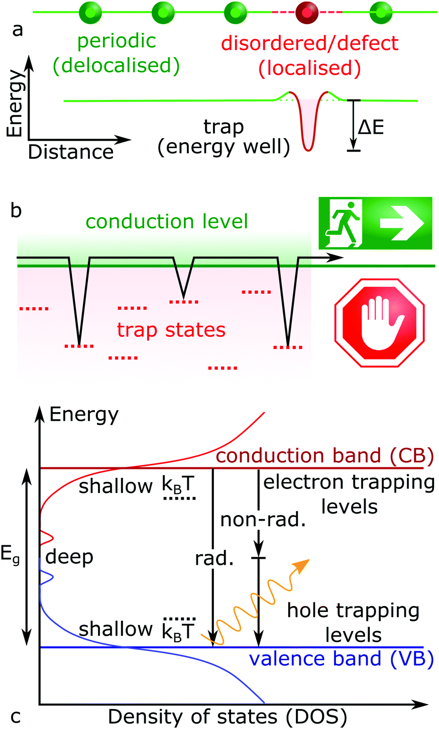 | ||
| Fig. 1 (a) Scheme of a charge localization caused by non-periodic disorder and defect in a semiconductor lattice (top), which introduce new energetic levels (bottom). (b) Scheme of charge trapping kinetics, where trap slow down charge carrier transport through trapping and detrapping events, as described by eqn (1). (c) Schematic representation of state density in a disordered semiconductor, whereby both band-to-band radiative (rad.) and non-band-to-band non-radiative (non-rad.) recombination (vertical arrows) can occur. | ||
The concentration of different defect types is determined by the enthalpy of their formation and the growth temperature.7 Despite the overwhelming advantages of LHPs, their ‘soft’ crystal lattice, and subsequent low defect formation energies,8 are expected to introduce relatively large concentrations of defects, which usually is detrimental to performance. However, the defect energy levels in LHPs favour the formation of relatively shallow and even benign states, making LHPs relatively tolerant9 to imperfections. Within this context, it is the unique ability to solution process high performance LHPs which is key to realizing their full potential, allowing for facile production options which are simply not paralleled elsewhere within semiconductor research. This difference is important because the performance of other common semiconducting materials branches10 (e.g. Si, Ge, and the III–Vs) are relatively sensitive to structural defects and must be grown under tightly controlled conditions (e.g. pure vapour deposition or high-vacuum epitaxy techniques).
The density of traps per unit volume and their relative energy in the electronic band structure strongly influence device performance, e.g. an increase in trap density and ΔE (towards mid-bandgap) directly decreases the carrier mobility and drops the open circuit voltage in solar cells.11 The trap density in LHPs has been shown to strongly depend on the (post-)processing procedures (such as annealing) employed,12,13 causing inconsistencies across different studies of the same material. Needless to say, the ongoing management and mitigation of parasitic defects (i.e. traps) in LHPs represents a scientifically challenging and technologically important task for researchers.14 Reducing their negative influence will ultimately lead to enhanced optoelectronic performance; for example, an almost trap-free LHP has been achieved in CsPbI3 quantum dots (QDs), yielding near unity photoluminescence quantum yields.15 Such trap-free conditions are reached by effective surface trap passivation (making the QD surface states unreactive) and by the improbability of a single bulk defect to be present per crystal (<10 nm). It is the aim of this review to clearly lay out the unique nature of charge trapping within lead halide perovskites, evaluate the current state of play within the field, and detail recent works which have aimed to identify their intrinsic and extrinsic origins, impacts and solutions.
Discussion
Influence of charge trapping
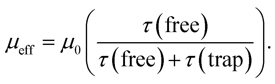
Under the influence of an electric field, charges in semiconductors drift according to the field direction through the crystal. This motion, however, is disturbed by scattering from phonons and lattice defects. Also charge carrier motion can be stopped by their capture on localized trapping states (Fig. 1b). Obviously, the captured charges do not contribute to net carrier transport while trapped. When captured on shallow traps at non-zero temperatures a charge can be thermally excited back to the transport band (above the so-called mobility edge) allowing it to contribute again to the net charge transport. Higher densities of free carriers in the system can also fill the traps with charges and increase the average charge mobility. Thus, the charge mobility of a semiconductor is a complex function of charge carrier concentration, trap types and their densities, thermal energies, the presence of scattering sites, and so on.In the presence of shallow traps, the multiple trapping and release (MTR) model is widely employed to describe charge mobility in crystalline semiconductors at room temperature. The effective mobility (μeff) is proportional to the trap-free mobility (μ0), reduced by the fraction of temporal trapping events:
 | (1) |
In addition, trapped charge carriers can be lost via trap-mediated non-radiative recombination (Fig. 1c), which decreases the energy conversion efficiency. This happens via trap states lying close to the middle of the bandgap (i.e. ΔE ≫ kBT). Indeed, deeply trapped electrons (holes) cannot be thermally excited back to the conduction band because the energy requirement makes the transition highly improbable, maximizing the probability of its non-radiative recombination with a hole (electron).
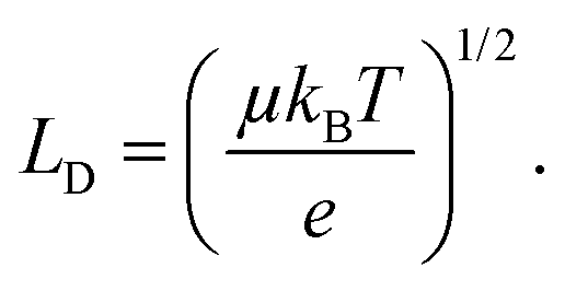
Non-radiative recombination is a highly parasitic process for solar cells because it limits the carrier diffusion length (LD) which, for a device to efficiently operate, should exceed the perovskite film thickness in order to be extracted. The diffusion length squared is proportional to the mobility mean (μ) and lifetime (τ) of charge e:
 | (2) |
Determining the nature of traps
Several types of defects are commonly identified within semiconductor crystals, being illustrated in Fig. 2(a) for the general ABX3 perovskite system.20 The imperfections shown in Fig. 2(a) are divided into two categories: intrinsic and extrinsic. Extrinsic surface defects – caused by the surrounding environment or unsaturated surface bonds – are a major concern in LHPs, as solution processed thin films often form grainy, polycrystalline networks. Intrinsic (or native) point defects are commonly branded using Kröger–Vink notation, whereby label MS identifies both the defective species (M) and lattice site (S). For instance, lead occupying an iodide site yields an anti-site label of PbI. The electronic band structure of LHPs is derived from the electronic Pb–X sub-lattice and most trap states will be directly linked to the energy levels created at improper bonding at these respective sites. For example, Fig. 2b shows how a bear X-terminating surface forms traps due to a lack of local stoichiometric composition and improper surface bonding (left), which can be mitigated by introducing a passivator (i.e. surface chemical treatment). For an effective passivation, new chemical bonds formed at the Pb–X-derived surface orbitals shift the defect level either toward or into the band edges, reducing the negative influence of the defect.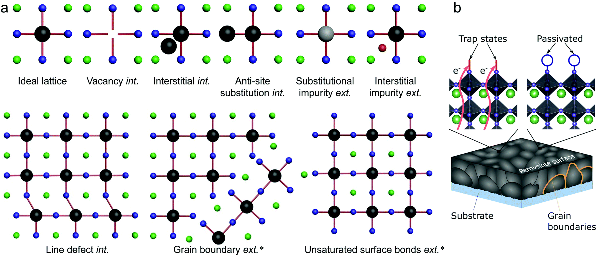 | ||
| Fig. 2 (a) Schematic overview of intrinsic (int.) and extrinsic (ext.) defect types in LHPs, relative to an ideal lattice. Defects which have been identified experimentally18,19 are indicated by ‘*’. (b) Schematic illustration of parasitic recombination at surface traps (and subsurface traps) being passivated by introducing additional atoms/molecules (blue circle) which binds to improperly bound orbitals, which cause the trap state. For all structures, the green, black and blue spheres represent A, B and X elements, respectively, while the grey and red represent different impurities. | ||
Solution-processed LHPs maintain relatively low trap densities21 in both polycrystalline (1016–1017 cm−3) and single crystalline (109–1011 cm−3) systems. An overview of the ranges determined experimentally for common lead halide perovskites22 is provided in Table 1. Compared to more traditional semiconductors, the values measured from LHP systems are fairly comparable; typical trap densities in polycrystalline23 (1013–1014 cm−3) and single crystal (∼108 cm−3)24 Si, compared to popular high-purity II–VIs and III–Vs, like CdTe (1013–1016 cm−3),25,26 CIGS (1011–1015 cm−3),27,28 GaN (∼5 × 1015 cm−3)29 and GaAs (1013–1015 cm−3).30
| Materials | Form (α phase) | Origins (calculation or experiments, trap density cm−3) | Solutions | |
|---|---|---|---|---|
| MAPbI3 | Single crystal | N (MAi, PbMA, VI, Pbi, MAI, PbI) | Intrinsic defects | (Intrinsic) tuning compositional ratio;13 K+ doping;65 anti-solvent63 |
| P (Ii, MAPb, VMA, VPb, IMA, IPb) | (nelectron = 4.8 × 10¹⁰, nhole = 1.8 × 10⁹)31 | |||
| First principle calculation35 | (ntrap = 3.3 × 10¹⁰),63 (3.6 × 10¹⁰)64 SCLC; (109–1010)64 TAS | |||
| Thin film | Intrinsic defects (5 × 10¹⁶) and surface defects (1.6 × 10¹⁷),66 (2.5 × 10¹⁷),67 (1017–1018),68 (6.7 × 10¹⁷)69 PL; (1015–1017),70 (1018–1019)71 TAS; (1.22 × 10¹⁶)72 SCLC; (1021)73 TSC | (Extrinsic) surface passivation (fullerene,70 pyridine and thiophene74) | ||
| FAPbI3 | Single crystal | N (FAi, PbFA, VI, PbI, FAI, Pbi) | Intrinsic defects (6.2 × 10¹¹),76 (1.13 × 10¹⁰),77 (1.34 × 10¹⁰)78 | (Intrinsic) introducing additional triiodide ions59 |
| P (Ii, FAPb, VFA, VPb, IFA, IPb) | SCLC | |||
| First principle calculation32 | ||||
| Thin film | 5.28 × 10¹⁴ | (Extrinsic) surface passivation (phenylalkylamine79), using PMMA80 | ||
| DLTS measurement;59 (1017)67 PL | ||||
| CsPbI2Br | Thin film | (8 × 10¹⁶),81 (1015–1016)82 SCLC | (Extrinsic) Pb2+ solution surface passivation81 | |
| CsPbI3 | Bulk | N (PbCs, CsI, PbI, Csi, Pbi, VI) | — | (Intrinsic) use TOP-PbI2 as reactive precursor15 |
| P (IPb, ICs, CsPb, Ii, VCs, VPb) | (Extrinsic) passivation (choline iodide,75 PVP83 and bidentate84 ligands) | |||
| First principle calculation41 | ||||
| MAPbBr3 | Single crystal | N (MAi, PbMA, VBr, Pbi, MABr, PbBr) | Intrinsic defects (nelectron = 1.1 × 10¹¹, nhole = 2,6 × 10¹⁰)31 (ntrap = 5.8 × 10⁹)63 | (Intrinsic) tuning molar ratio;87 anti-solvent63 |
| P (Bri, MAPb, VMA, VPb, BrMA, BrPb) | SCLC measurement; (ntrap = 1015)85 PL measurement; (ntrap = 109)86 DLTS | (Extrinsic) passivation (amine-based88 passivation) | ||
| DFT calculation33 | ||||
| FAPbBr3 | Single crystal | — | Intrinsic defects (9.6 × 10⁹)77 | (Intrinsic) rubidium doping89 |
| SCLC measurement | (Extrinsic) organic ligands treatment90 | |||
| CsPbBr3 | Single crystal | N (CsBr, Csi, Pbi, PbBr, PbCs, VBr) | Intrinsic defects (nelectron = 1.1 × 10¹⁰, nhole = 4.2 × 10¹⁰)91 | (Intrinsic) tuning precursor concentration92 |
| P (BrCs, BrPb, CsPb, Bri, VCs, VPb) | SCLC measurement | (Extrinsic) post synthesis treatment with lead bromide;93 thiocyanate94 surface passivation | ||
| First principle calculation9 | ||||
Each experimental technique used to examine traps has its own advantages and limitations. The popular space charge limited current (SCLC) method31 is widely used for LHPs and provides many of the values in Table 1, offering a powerful method for unravelling carrier transport properties, like the carrier density, conductivity, mobility and trap concentration. However, while SCLC is widely used to characterise LHPs, trap concentrations determined in this way are imperfect, as the approach cannot discriminate between different kinds of charges generating the current.22 For example, LHPs have the potential for ion transport within the crystal, which leads to an underestimation of the trap concentration. This is particularly true for the relatively low trap concentration range (i.e. 108–109 cm−3). Roughly speaking, if the concentration of mobile ions is enough, they can compensate the effect of traps on the current.
With the trap population experimentally evaluated, effort must be made toward understanding their cause. Theoretical calculations – including ab initio and density functional theory (DFT) methods – provide one of the most powerful and direct tools for exacting the nature and origin of traps. This is because it is practically impossible for experimental probes to reliably provide an atomistic picture of the imperfection, and thus must be complemented via predictive materials modelling. A classical approach takes the form of calculating the energy level of the defect and comparing it to the calculated electronic band structure.34 Though, depending on the calculation method employed, the reliability of DFT for investigating defect states still remains in question.37–39 For DFT calculations of defect energy levels, supercells are typically employed with a large number of atoms and high computational costs. This encourages the use of faster DFT routines, such as methods which exclude spin–orbit coupling (SOC), functionals which correct for self-interaction error and hybrid functionals (i.e. HSE-06 or PBE0), which contain a fraction of the Hartree–Fock exchange, as opposed to functionals which do not include it (i.e. generalized gradient approximations: GGA). Du et al. showed40 that neglecting SOC and hybrid functions in some of the early DFT calculations reported for LHPs lead to incorrect predictions of the electronic band structure.40 As an example, for MAPbI3 GGA gives a gap of 1.6 eV, GGA + SOC gives 0.6 eV, HSE-06 gives 2.4 eV and HSE-06-SOC gives 1.6 eV. The value determined using HSE-06-SOC is accurate and places the relative band edge energies correctly, while GGA which gives the same gap though the wrong band energies (all levels are shifted up by roughly 0.5 eV), implying inaccurate defect levels. As such, Agiorgousis et al. reported38 deep intrinsic defects in MAPbI3, including iodine vacancies, while Du et al. claimed that iodine vacancy will only create shallow traps.37 Ultimately, iodine vacancies were confirmed through reliable DFT calculations40 to cause relatively shallow charge trapping.
Defect energy simulations for LHPs are relatively limited and there is certainly no systematic or complete set of results covering the different cation and halide compositions. Fig. 3 overviews the predicted energy levels for all 12 native point defects in lead halide perovskites, determined using DFT9,32–34,41,42 (with SOC where available9,41,42). A central issue here is in the accuracy of the quantitative prediction of the band edges, which is essential to reliably estimating the relative defect energies. This problem is pronounced for the DFT calculation of the CsPbI3 perovskite (with SOC), with the bandgap estimated at 1.02 eV,41 which is far less than experimental observations44 (1.8 eV). Excluding SOC in the calculation leads to a larger bandgap energy of 2.0 eV,44 highlighting the dependence of the result to the method employed.39
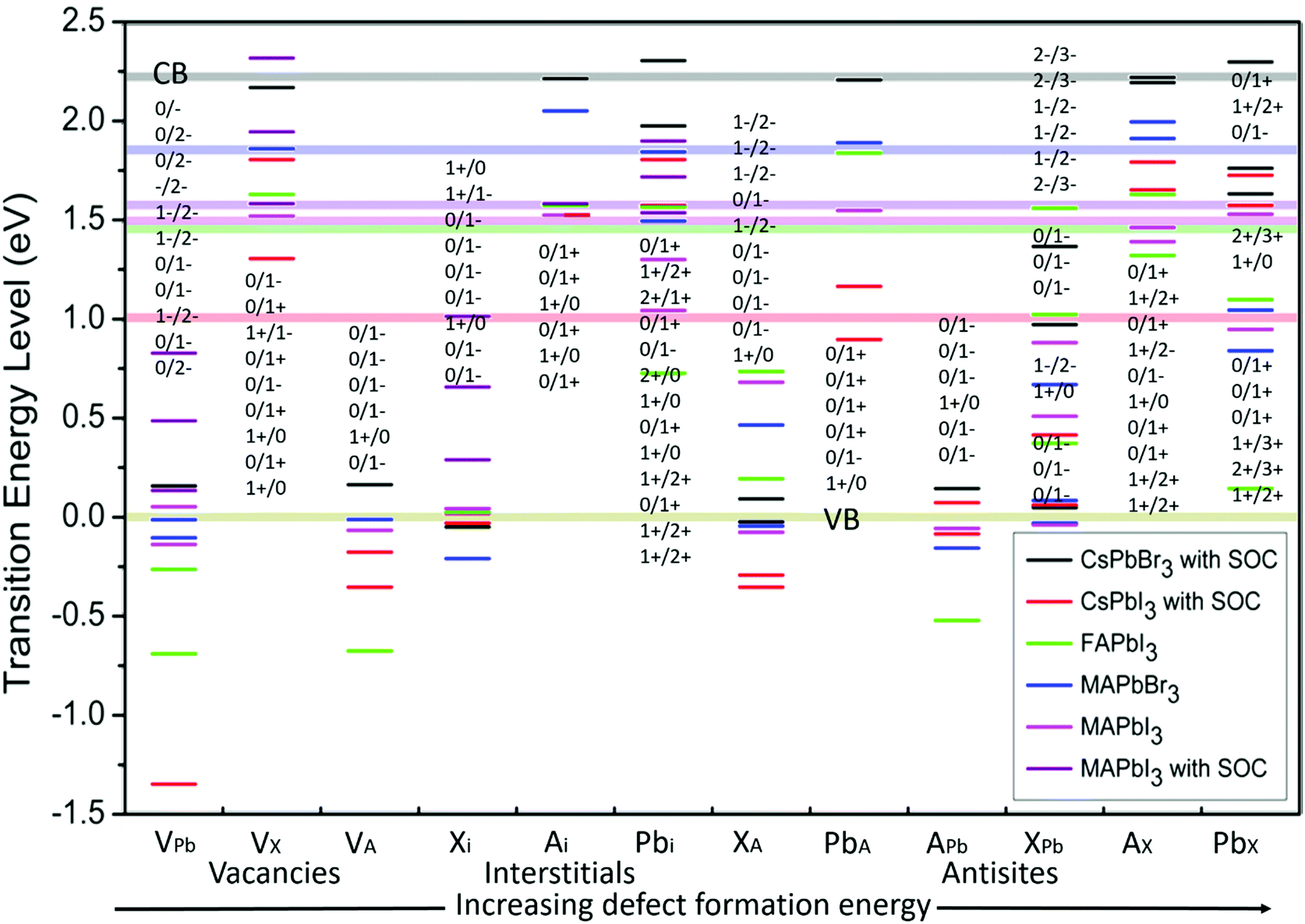 | ||
| Fig. 3 The calculated transition energy levels of intrinsic point defects9,32–36 in APbX3 perovskites. The energy is determined relative to a zero-energy valence band for all materials, with the same color scheme used to show the position of the conduction band (semitransparent horizontal lines). The defect levels are identified in terms of the threshold energy to convert the system from charge state q to q′, in the format q/q′. For example, if q′ is less (more) than q, the defect acts as an electron acceptor (donor), with the integer difference indicating the number of trapped charges. From left to right, the point defect types are placed in a general order of increasing formation energy. | ||
Fig. 3 horizontally places the different defect types in LHPs roughly in order of increasing formation energy,39,45i.e. or decreasing probability of forming within the crystal. In general, shallower traps are more inclined to arise from a vacancy and interstitial defects in LHPs, which typically have the smallest formation energy. Conversely, deep traps arising from anti-sites are likely to form less frequently. This helps to explain, in part, how even LHP polycrystalline thin films retain good optoelectronic properties, compared to their relatively less defective SC counterparts.
Intrinsic point defects and defect tolerance
Theoretical studies of LHPs have mainly focused on well-ordered structures, such as the well-defined α, β, γ and δ phases of lead-based systems.46 In reality, perovskite structures are inherently disordered and very complicated. This is particularly true when they are integrated into a mesoporous network, e.g. titania, alumina or any other substrate for device applications. It has been suggested that the majority of MAPbI3 perovskite films integrated with mesoporous TiO2 (70%) are disordered, where their local structural coherence extends over a range of only ∼1.4 nm.47 Even high-quality perovskites possess an intrinsic level of disorder on the same length scale, due to its soft crystal structure and complicated lattice dynamics.48–51 The dynamic disorder of LHP is related to local thermally driven distortions in the lead halide framework.52 Furthermore, there is evidence14,53 of a potential direct relation of ion migration with parasitic nonradiative recombination centers. Overviews of important studies identifying and controlling the ion migration process can be consulted in reviews.54,55 For example, the ultrasoft and polarisable lattice of the α-FAPbI3 system produces polarons (through electron–phonon coupling) with a coherence length similar to the 1.4 nm described above, without any connection to the material being in a mesoporous matrix or not.56DFT is currently the most accepted technique for targeting and isolating the origin of point defects. As outlined above, such work has helped to reveal why LHPs exhibit a relatively strong tolerance to crystal defects and traps,33 compared to more traditional semiconductors. Though, no reports have managed a series of controlled and direct experimental results. DFT calculations suggest the relative energies for many intrinsic point defects in LHPs collect near to, or even inside, the electronic states forming the CB and VB (Fig. 4). This is because point defects which introduce deep mid-gap states (i.e. large ΔE) are unlikely to form, enabling reasonable carrier release energies and subsequently short trapping times at room temperature. The close proximity of defect energy levels57,58 in LHPs relative to the CB and VB is expected to arise from having molecular anti-bonding orbitals (which raise the energy of the orbitals) at the (valence band maximum) VBM, and bonding orbitals at the (conduction band minimum) CBM. This is in contrast to traditional semiconductors, which typically have the reverse orbital character. Taking an atomic vacancy as an example, this concept can be clarified; dangling bonds at a vacancy (of any type) establish levels inside the VB and near the CB,2,57,58 leaving the bandgap relatively clean. This argument can be extended to other types of intrinsic defects, such as interstitials and anti-sites, as well as the dangling bonds found at grain boundaries and surfaces. This is in contrast to more traditional defect intolerant systems like the classic III–V semiconductor band structures (Fig. 4), which are more prone to deep trap formation. According to the relative energy of the trap states in the bandgap, their characterization can be further subdivided into electron acceptors (p-type) and donors (n-type).
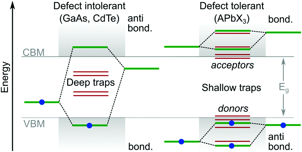 | ||
| Fig. 4 Comparison of typical trap energies relative to the electronic band structure of traditional defect intolerant compound semiconductors (i.e. III–V and II–VI varieties) and defect tolerant43 lead halide perovskite materials.1,2 | ||
Table 1 provides a summary of point defect traps revealed in a variety of popular lead halide perovskite compositions. Through this table, common intrinsic trap types and their effects can be found, and used to predict the properties of other lead halide perovskites. For example, halide interstitials and the substitution for A cation and Pb typically induce hole traps (electron donors). In contrast, halide vacancies and A cation substitutions for halide usually induce electron traps (electron acceptors). Thus, the nature of traps within the electronic structure of performant lead halide (iodide-based) systems appears to be relatively consistent across varied cations compositions.
FAPbI3-based perovskite materials have been involved with recent reports of high-performance perovskite solar cells, i.e. all devices exhibiting conversion efficiencies in excess of 18%59–61 (see Fig. 4). DFT modeling of FAPbI3 has revealed that their intrinsic defects levels are relatively similar to those existing in MAPbI3.32 This is expected, given their common Pb–I hybridised electronic structure; the upper valence band is formed by Pb s and I p orbitals and the conduction band are predominantly made by the Pb p orbitals. However, weaker van der Waals interactions between the FA cations and the PbI6 octahedra can create deep levels of FA-related traps (e.g., FAI and IFA) in the band gap.32 Thus, the MA and FA A-site cations in perovskites do not directly contribute to the electronic states in the vicinity of the band edges. A-cation-related intrinsic defects (vacancies or substitutions) will not directly induce mid-gap traps, though can influence the defect formation energies of the nearby lead halide octahedral. Actually, A-site cation defects have an indirect effect on optical and electronic properties of perovskite materials by changing the lattice parameters or octahedral tilting, locally, thereby affecting the Pb–X sub-lattice.
Nonetheless, taking MA/FAPbI3 mixed cation perovskites together as a joint case study, shallow traps, deep traps and trap levels induced by charged defects will exist to varying degrees. The ideal MAPbI3 structure intrinsically exhibits twelve point defects including vacancies of MA, Pb and I, interstitial MA, Pb and I, and six substitutions being MAPb, PbMA, MAI, PbI, IMA and IPb. Despite competing interpretations,37–39,62 point defects in MAPbI3 are expected to only induce shallow transition energy levels. Although, deep level trap states can form by Ii (iodide interstitial) in β-MAPbI3.40 Further, it has been shown that excess iodine, in the form of MAI and PbI2 vacancies, do not create any parasitic trap states.22
Charged point defects
The effects of charged defects, and specifically highly mobile ions, in MA/FAPbI3 has become an important research topic and attracted recent attention.49,95 This is because the migration of ionic defects with low activation energies forms an intrinsic mechanism inside perovskites,95 with the notable exception of Pb2+ migration49 (activation energy is generally considered too large). Consequently, iodine vacancies (interstitials) in MAPbI3 are particularly influential in optoelectronic devices, as they can easily diffuse through the perovskite crystal while exposed to an external bias.49,96,97 Charged defects are considered as the origin of elemental redistribution within perovskites and have been linked to local changes in density of states and electrical properties.54 For instance, ion migration is the likely origin of the photocurrent hysteresis effect49 and giant switchable photovoltaic effect98 in solar cells. While charged migrating ions themselves do not necessarily contribute to charge trapping, LHPs are increasingly being considered as “soft” solids and such phenomenon contributes and complicates the environment in which defects form and influence carriers deep inside the crystal.99Formation and mitigation of intrinsic defects
The formation of point defects during perovskite growth are governed by the crystallisation kinetics and dynamics. The relationship between defects and the growth conditions has been extensively investigated and revealed to be highly multi-parameter problem. Together, the material stoichiometry, light exposure, temperature, atmospheric humidity and pressure are all found to influence the formation of defects.12,100,101 Wang et al. demonstrated that both thermal treatments and tuning the molar ratio of the precursor agents (PbI2 and MAI) during solution deposition can reduce the final trap density.102 Further, thermal annealing can also convert a p-type perovskite to n-type, by removing MAI. Conversely, the hole concentration can be reduced by adjusting the MAI concentration forming p- or n-type perovskites when applying a two-step solution process. Similar work is also reported by Divitini et al.103 where they found that heat treatment can lead to iodine and lead migration under extremely high temperatures, stabilizing the perovskite layer. Further exposure to small amounts of oxygen can also help interstitial iodine oxidation and decrease deep level trap density.104Compositional alloying has proved an efficient way to suppress traps in LHPs through the possibility of phase separation into low defect phases.105 Unfortunately, the exact nature of defects in alloyed perovskites are still unclear. In any case, it was recently reported that doping APbI3 with alkali cations (Rb+, K+)106,107 has several beneficial effects to help mitigate defect formation and charge trapping. The introduced K+ can occupy interstitial sites in MAPbI3 and create MA vacancies.65,108 As such, the presence of K+ can modify the physical and electrical properties and prevent iodide defect formation. Importantly, the hysteresis effect within solar cells can also be reduced by introducing K+ cations. It is further demonstrated that the optimized amount (20%) of K+ could help for improving crystallinity and decrease surface potential in MAPbI3 films. In a similar fashion, halide doping with Br− and Cl− can effectively inactivate iodine hole traps.42
Light soaking and trap filling
So-called “light soaking” effects – where the photovoltaic output is altered during light exposure – have been observed in a variety of solar cell technologies, influencing their long-term performance under illumination.109 For instance, amorphous silicon (a-Si) exhibits a few percent decrease in PCE after the first hundred hours of light soaking due to defects created via breaking of the Si–Si bonds by the photo-excited carriers after thermalization.109–112 For the case of CdTe- and CIS/CIGS-based (i.e. Cu(In,Ga)Se2 family) photovoltaics, light soaking enhances the device output by filling trap states which form in the dark. For the relatively dynamic LHP semiconductor family, several studies have reported changes in the perovskite trap density following controlled exposures to light.100,113–117 Due to features like light-induced ion migrations and compositional redistribution, the underlying mechanisms altering the trap density upon light exposure are still under debate especially when it concerns the effect of the environment (oxygen, water etc.) on the process.100,113–117 Some studies report a reduction of the overall trap density upon light soaking, due to either annihilation of iodine vacancies and interstitials.113 Others report a similar response, though connect it with iodine migration.118 On the other hand, light-activated degradation of the device photocurrent has been observed, and subsequently reverses through a self-healing process when left in the dark.100 Each of these cases must be considered independently (being strongly dependent on material engineering and processing), making it difficult to set a standard in the stabilization requirement of different devices under working conditions.Extrinsic defects and traps
Traditional low-temperature solution processing can readily introduce impurities into the crystal bulk during crystallization, attributable to localized stoichiometry deviations. Unintentional contamination of the synthesis solution can also cause substitutional impurities with foreign elements and compounds. An incorporated impurity can promote point doping or lattice vacancies, interstitials and substitutions, which can introduce traps (often relatively deep) into some LHP band structure structures.119–121 The exact nature of extrinsic defects arising from synthesis-derived impurities are inherently varied and complex,119,122 and are not dealt with here in detail.Two dominant sources of extrinsic defects in LHP thin films occur at the grain boundaries (GBs) and the terminating surface states, due to the widespread application of grainy spin coated thin films. Examining Table 1 there is a large difference between the trap densities expressed by LHPs in single crystalline and thin film forms. As a clear example, MAPbI3 single crystals show a much lower defect density (1010–1011 cm−3) than spin coated thin films (1016–1017 cm−3), a difference directly attributable to extrinsic effects, i.e. the introduction of far more relatively disordered surface areas. As a consequence, LHP large single crystals also exhibit much higher carrier mobilities and longer diffusion lengths,123 compared to their polycrystalline counterparts.
The kinds of defects that can form at GBs and on the perovskite surface are far more varied than the intrinsic point defects found in the crystal bulk. The diversity of improper bonding options at GBs and surfaces increases the contribution of parasitic deep traps and nonradiative recombination losses.124 Unchecked, deep traps formed at the GB will dramatically destroy solar cell efficiencies. For example, Chen et al.124 passivated GB traps in thin film MAPbI3 by releasing the organic species during annealing, resulting in enhanced carrier lifetimes and a dramatic rise in photoconversion efficiencies (from 0.7% to 12%).
Unlike intrinsic point defects which typically require insights from computation modelling, GBs and surface traps can be studied directly using experimental microscopy techniques (often optical- and electron-based), and sorted through effective material proccessing choices.125,126 Through direct observations, it has been discovered that a substantial portion of the total traps accumulates at the grain interface. Edri et al.127 studied the effect of GBs in MAPbI3 and reported that the work function energy (i.e. energy required to liberate an electron into the conduction band) is higher at the GBs, with the average grainsize being controllable through halide substitution/mixing. Also, they found that improper I–I chemical bonds formed at GBs is a consequence of extremely large lattice constant due to large A and B atoms in halide perovskites, a finding supported by first-principle calculations.128 On the other hand, studies utilising Kelvin probe force and conductive atomic force microscopy showed that GBs might actually be helpful for charge carrier separation, because of a potential barrier along the GBs.129
Rather than chemically passivating surfaces and GB trap states, several morphology-based techniques have been developed to reduce their effect. For instance, solvent treatment during thermal annealing process can efficiently increase the crystallinity and grain sizes of MAPbI3125 and help seed homogeneous film growth across the substrate, resulting in an almost uninterrupted vertical grain formation.130 The formation of vertical grains reduces the projection of the GB surface “seen” by charges being internally screened and extracted by the applied electric field. Combined with a perovskite seeding method, the effect of GBs can be reduced by forming large grain sizes and orienting the crystal grains, to achieve 21.5% power conversion efficiencies.130
Surface defects at the heterojunction
The active planar perovskite layer in solar cells forms a heterogeneous junction (heterojunction) on its top and bottom surfaces, where the hole and electron transport layers of the device interface. Both unbound and improperly bound atomic orbitals occur due to a lack of stoichiometric compositions, introducing localised states. When optimising device performance, it is at the perovskite surface where a substantial number of issues regarding carrier trapping and transport,131,132 can potentially be improved. This results from the sheer number of different types of defects and trap introduced at heterojunctions. Surface states often provide deep mid-gap traps for charge carriers, resulting in non-radiative recombination pathways and contribute as the main origin of undesirable photocurrent hysteresis effects.70,133 Very recently, Jiang et al. established134 a new record (held briefly) for perovskite solar cell conversion efficiency, certificated at 23.32%. This advance was achieved by the use of an organic halide salt phenethylammonium iodide (PEAI) on HC(NH2)2–CH3NH3 mixed perovskite films, for the passivation of deep surface traps. Similarly, the concentration of surface trap states was reduced using choline iodide with a new achieved efficiency75 in inorganic LHPs at 18.3%. Shao et al.70 managed to eliminated operational hysteresis by suppressing trap density (on GBs and surface) by fullerene. By controlling the average size of the individual grains, hysteresis effects related to surface traps have also been countered.126,135 In the end, studies on the origin of the surface traps in perovskites involving lead iodine complexes point toward undercoordinated I ions being responsible for deep surface traps136 (generally depicted in Fig. 2(b)), though further work is required to confirm. Other more exotic solutions have also been shown effective to further decrease surface trap densities; passivating surface traps via adsorbates (oxygen, water, thiols), Lewis bases74 like pyridine and thiophene (also called ligand treatment passivation), and supramolecular halogen bond complexes.136Hollow perovskites
It is also necessary to discuss the potentially positive effects of defects in MHPs. As we know, there are several ways to tune the bandgap140 in LHPs including halide doping and changing the material dimensions from 3D to 2D. The intentional incorporation of small molecules in 3D perovskites (ethylenediammonium141) can promote lead and halide vacancy formation in the 3D structure, creating a less connected perovskite structure and a blue-shift in the direct bandgap.141,142 The less dense 3D perovskite is commonly called a hollow perovskite, and provides a fundamentally new way to manipulate perovskite intrinsic properties through defect engineering, without changing dimensionality or halide composition. Most importantly, hollow perovskites exhibit improved air stability141 compared to their unmodified counterparts and allow for efficient solar cells (∼17%; Pb/Sn-based). Such efficiencies are only made possible by the fact that the widespread incorporation of defects which hollow out the 3D structure does not introduce large trap-state densities. For example, Ke et al.143 showed that lead-free perovskite MASnI3 which is loaded with 15% ethylenediammonium has ∼50% lower electron trap-state density than thin films processes without loading, resulting in ∼9 times longer carrier lifetime. Similar reductions in trap densities were revealed for the mixed Pb/Sn-based perovskites,144 indicating that the benefits of this approach can potentially be extended to LHP solar cells.Lead-free halide perovskites
Because of the toxicity of Pb-based materials and their instability with heat and moisture, Pb-free LHP systems are increasingly being considered for optoelectronic applications, i.e. involving elements like Sn, Ge, Bi and Sb. Unlike the beneficial defect tolerance found in the band structure of lead halide perovskites (Fig. 4), Pb-free systems express a very different landscape for defects and specifically charge trapping. For example, Sn-iodide perovskites exhibit an extremely high hole density because of shallow transition levels (selecting for electrons) caused by a high concentration of Sn vacancies.145 This effect is quite significant, where Sn-based perovskites exhibit exotic self-doping properties, transitioning from semiconductor-like to more metallic.146,147 Coincidently, a similar problem is found in the Ge halide perovskite branch, which also exhibit high hole densities.148 Double perovskites (general chemical formula A2BB′X6) based on trivalent Bi3+ and Sb3+ exhibit relatively large bandgaps, however generally inferior fundamental properties because of differences related to reduced crystal and electronic symmetry.149 Although those properties are undesirable for photovoltaic and EL devices, double perovskites exhibit some novel applications, such as high sensitivity X-ray detectors.150–152 For instance, Cs2AgBiBr6 has been shown to have traps selecting for electrons at room temperature (promoting a p-type nature), which can be significantly suppressed at lower temperatures, while retaining a cubic perovskite symmetry (unlike the APbI3 systems, which generally undergo a series of symmetry lowering distortions).153 For double perovskites, tuning the composition appears to be the main way to reduce the influence of defects in double perovskites.154 For example, the Ag-rich and Br-poor condition is preferred for n-type Cs2AgInBr6 with shallow trap energy level. Similarly, Br-poor/Bi-rich are beneficial for reducing deep energy defects in the Cs2AgBiBr6 bulk, the surface extrinsic traps make the dominant contribution of charge recombination in Cs2AgBiBr6 photovoltaic devices.Outlook and discussion
Trap management progress and solar cell efficiency trends
While single-junction solar cell efficiencies over 20% have been realised in recent years (Fig. 5), this is still well below the thermodynamic limit of ∼31% for MAPbI3 or the Shockley–Queisser limit (∼33%). Evidently, there is still quite some room for improvement and a large portion of this possibility resides in the negative influence of traps. Following the seminal reports of dye-sensitized perovskite solar cells in 2009 and 2012 (Fig. 5), there appears to be two separate trends for the types of scientific breakthroughs which have been driving up the reported conversion efficiencies of perovskite based solar cells. Between 2013 and 2016, solvent engineering and refining grain formation, together with compositional tuning for suitable bandgaps and stability, facilitated massive gains in device performance60,80,120,137,138 (Fig. 5). The large technological advances made during this early development were realised via improved materials processing, to harness the intrinsic potential of LHPs within photovoltaics. More recently, since 2016, researchers have had to shift their focus toward trap management, in the interest of harnessing the remaining potential efficiency contained in LHP solar cells. For this, reducing the trap populations in all their forms (both intrinsic and extrinsic), and their negative influence on devices, has seen a steady, albeit slower, rise in efficiencies.59 A lack of precise control over the crystallization process will introduce some unwanted defects. By using PMMA as a template to control crystal growth, larger grain size and oriented microstructure can be obtained80 with an efficiency of 21.02%. Vacancies in LHP point defects are most likely shallow defects because of their low formation energies. But interstitial and antisite defects may be responsible for nonradiative recombination. Through the introduction of additional iodide ions into the organic cation solution, the efficiency record was advanced decreasing deep traps (interstitial and antisite defects) in the bulk and achieving a certified 22.1% efficiency.59 By July 2017, the record was further updated to 22.6% using fluorene-terminated materials as hole transport layer, passivating interfacial traps.61 As we discussed, surface defects often result in deep mid-gap traps for charge carriers. Similarly, surface trap passiviation134 (via PEAI salt introduction) allowed for an efficiency of 23.3% in 2018. As of now, the new record of 25.2% was recently confirmed by NREL139 (Fig. 5), though the details of the device are yet to come out. Moreover, a new efficiency record75 of 18.3% was achieved for pure inorganic CsPbI3 by reducing surface traps via choline iodide.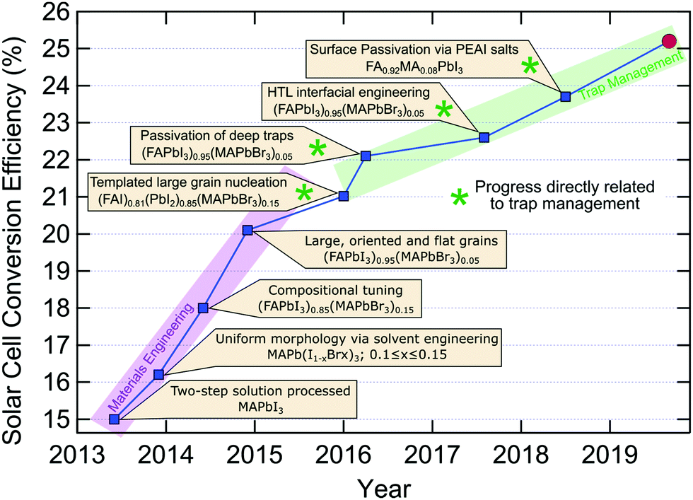 | ||
| Fig. 5 Overview of recent progress in single junction perovskite solar cell efficiency, identifying the key technological advances.59–61,75,80,120,134,137,138 The red circle indicates the current record (25.2%) confirmed by National Renewable Energy Laboratory (NREL).139 | ||
All-optical techniques for probing polycrystalline LHP thin films
All methods used to experimentally probe defect states are based on measuring different physical phenomena which are in some way connected (often indirectly) to charge trapping. For example, electrical transport measurements often cannot distinguish between relatively shallow traps (simply acting to slow down charge transport) and non-radiative centres and deep traps, which facilitate fast non-radiative charge recombination. The higher the charge injection rate, the smaller the contribution of trapping to the overall charge dynamics due to trap filling. Therefore, even quite defected materials can still work well in the high injection rate regime.66 If fact, the trap filling effect can be used to assess the trap concentration by measuring PL decay dynamics as a function of excitation power density.115 Note, however, this method relies on the modelling employed, which in turn requires prior knowledge of recombination mechanisms, doping concentration and other parameters, which are usually not available. Obviously, each technique for trap detection has its sensitivity limits, assumptions and artefacts which must not be forgotten.It is educational to inverse the trap concentration and calculate the volume of the crystal containing just a single trap state, as shown in Fig. 6. Taking the cubic root of the concentration, values from 1015–1012 cm−3 correspond to one defect per cubic volume possessing side lengths of 100 nm and 1 μm, respectively. It is the relatively large charge carrier diffusion length in LHPs (as high as micrometers) which allows all carriers to be affected by traps, even when they are relatively far apart from each other. As such, these factors have recently combined (i.e. a desire to exhaust all trap passivation options, together with the complementary length scales of both optical probes and low trap concentrations) via the emergence of several interesting studies into non-radiative carrier recombination in LHP, centered on optically-based imaging. First of all, large variations in PL intensity are observed locally across a thin film by PL microscopy, which infers that the concentration of the defects is different from one optically-resolved spatial location to another.117,155–157 In addition to that, local areas of LHP films often show PL intensity fluctuations, flickering or even blinking – the phenomenon which is clearly observed in nano and micro crystals of these materials.117,157–161 From the body of available literature, PL blinking appears to be a general consequence of softness, chemical reactivity, ion migration and “self-healing” properties of LHPs leading to reversible formation of metastable non-radiative centers.158,162–164 Thus analysis of PL intensity fluctuations is an efficient way to detect strong non-radiative centers present in small numbers of LHP crystallites, which has been also successfully used to study graphene oxide.165 PL blinking also allows for spatial localization of the activity of metastable non-radiative centers beyond light diffraction limit using optical super-resolution.157–160,162,166 Unfortunately these pure optical imaging methods can detect and count of metastable defects only, while the presence of permanent traps can be seen only indirectly, e.g. by PL lifetime.
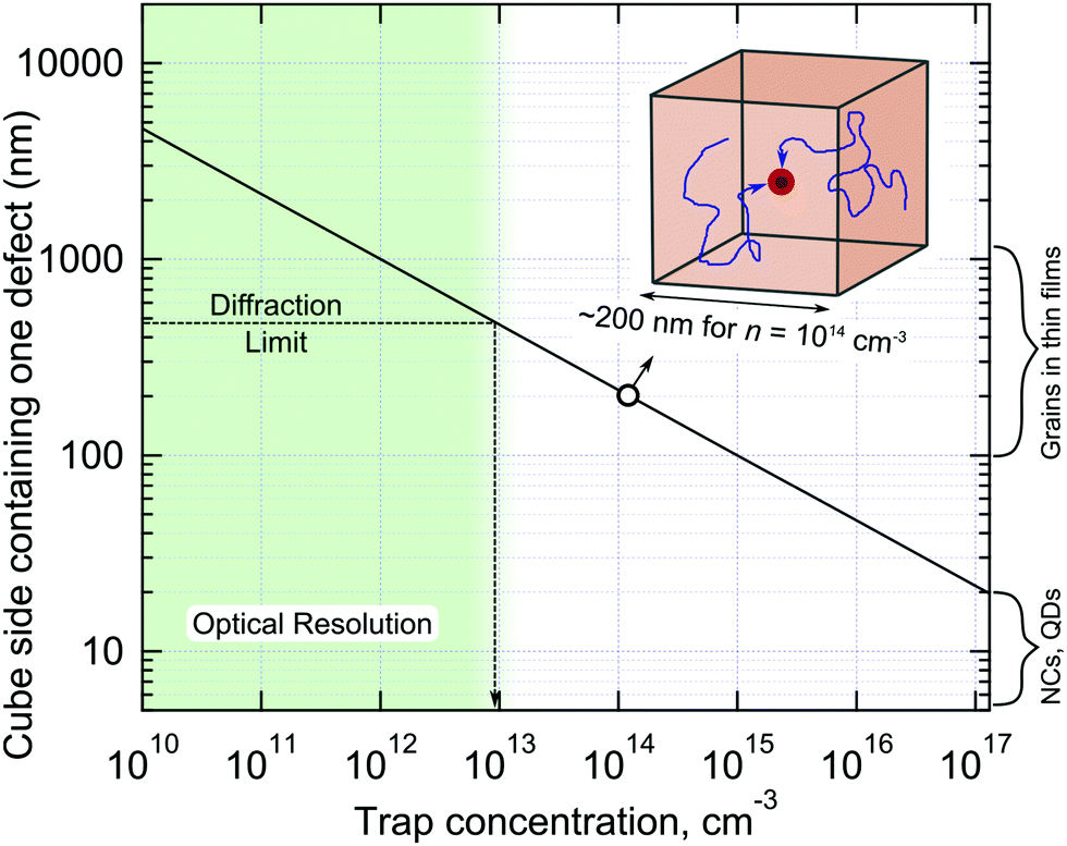 | ||
| Fig. 6 Dependence of a single defect containing cube side length on the defect concentration. The inset shows that the migration of carriers within the cube-shaped volume makes all charges in the volume affected by the presence of the defect. Note that for QDs or nanocrystals (NCs) to possess one defect per crystal the concentration of the deep traps should be as large as 1017–1018 cm−3, which explains the practical absence of non-radiative processes in such small crystal. The resolution of PL microscopy is about 500 nm which allows for observation of the defect states in films via inhomogeneous PL spatial distribution for n < 1014 cm−3. | ||
Conclusion
Although it is a tedious task to fully understand the nature and cause of charge trapping in lead halide perovskites, localising their influence and developing principles to mitigate their effects are crucial for reducing device losses. Combining theoretical and experimental approaches has thus far proven powerful in revealing the major issues. This has ultimately shaped the progress made in solar cell device efficiencies in recent years, and will likely continue to play a large role in the future. Important gaps in our current understanding still include the precise identification of intrinsic and extrinsic defects. While the extrinsic effects involving LHP surfaces and GBs have been recognised by direct observations, and sometimes confirmed by materials modeling, typically point defects are parsed computationally. Central to the success of LHP thin films are their beneficial tolerance to defects, which is why the unusual behaviour of localised states in these semiconductors is so important to understand. Through ongoing efforts to control and engineer traps in LHP thin films, the power conversion efficiencies in solar cell devices will increase, and continue to approach their thermodynamic limit.Conflicts of interest
The authors declare no competing financial interest.Acknowledgements
The authors acknowledge financial support from the Research Foundation-Flanders (FWO, grant numbers G098319N, G.0962.13 and ZW15_09GOH6316) and postdoctoral fellowship to J. A. S., M. K. and E. D. (grant numbers 12Y7218N, 12Y6418N and 12O3719N, respectively), the KU Leuven Research Fund (C14/15/053), the Flemish government through long term structural funding Methusalem (CASAS2, Meth/15/04) and the Hercules foundation (HER/11/14). The authors thank the Swedish Research Council, Knut and Alice Wallenberg foundation. We would also like to express our sincere thanks to Filippo De Angelis and David Egger for their helpful discussions.Notes and references
- M. V. Kovalenko, L. Protesescu and M. I. Bodnarchuk, Science, 2017, 358, 745–750 CrossRef CAS.
- R. E. Brandt, V. Stevanović, D. S. Ginley and T. Buonassisi, MRS Commun., 2015, 5, 265–275 CrossRef CAS.
- R. Service, Science, 2016, 354, 1214 CrossRef CAS.
- J. A. Christians, P. Schulz, J. S. Tinkham, T. H. Schloemer, S. P. Harvey, B. J. T. de Villers, A. Sellinger, J. J. Berry and J. M. Luther, Nat. Energy, 2018, 3, 68 CrossRef CAS.
- A. Peaker, V. Markevich and J. Coutinho, J. Appl. Phys., 2018, 123, 161559 CrossRef.
- V. Abakumov, V. I. Perel and I. Yassievich, Nonradiative recombination in semiconductors, Elsevier, 1991 Search PubMed.
- D. Vinichenko, M. G. Sensoy, C. M. Friend and E. Kaxiras, Phys. Rev. B, 2017, 95, 235310 CrossRef.
- A. Walsh, D. O. Scanlon, S. Chen, X. Gong and S. H. Wei, Angew. Chem., Int. Ed., 2015, 54, 1791–1794 CrossRef CAS PubMed.
- J. Kang and L.-W. Wang, J. Phys. Chem. Lett., 2017, 8, 489–493 CrossRef CAS PubMed.
- V. Eremin, E. Verbitskaya and Z. Li, Nucl. Instrum. Methods Phys. Res., Sect. A, 2002, 476, 537–549 CrossRef CAS.
- I. J. Kramer and E. H. Sargent, ACS Nano, 2011, 5, 8506–8514 CrossRef CAS PubMed.
- P. Fassl, V. Lami, A. Bausch, Z. Wang, M. T. Klug, H. J. Snaith and Y. Vaynzof, Energy Environ. Sci., 2018, 11, 3380–3391 RSC.
- Q. Wang, Y. Shao, H. Xie, L. Lyu, X. Liu, Y. Gao and J. Huang, Appl. Phys. Lett., 2014, 105, 163508 CrossRef.
- S. D. Stranks, ACS Energy Lett., 2017, 2, 1515–1525 CrossRef CAS.
- F. Liu, Y. Zhang, C. Ding, S. Kobayashi, T. Izuishi, N. Nakazawa, T. Toyoda, T. Ohta, S. Hayase and T. Minemoto, ACS Nano, 2017, 11, 10373–10383 CrossRef CAS PubMed.
- C. Wehrenfennig, G. E. Eperon, M. B. Johnston, H. J. Snaith and L. M. Herz, Adv. Mater., 2014, 26, 1584–1589 CrossRef CAS PubMed.
- S. D. Stranks, G. E. Eperon, G. Grancini, C. Menelaou, M. J. Alcocer, T. Leijtens, L. M. Herz, A. Petrozza and H. J. Snaith, Science, 2013, 342, 341–344 CrossRef CAS PubMed.
- B. Yang, O. Dyck, J. Poplawsky, J. Keum, A. Puretzky, S. Das, I. Ivanov, C. Rouleau, G. Duscher, D. Geohegan and K. Xiao, J. Am. Chem. Soc., 2015, 137, 9210–9213 CrossRef CAS PubMed.
- R. Ohmann, L. K. Ono, H.-S. Kim, H. Lin, M. V. Lee, Y. Li, N.-G. Park and Y. Qi, J. Am. Chem. Soc., 2015, 137, 16049–16054 CrossRef CAS PubMed.
- J. M. Ball and A. Petrozza, Nat. Energy, 2016, 1, 16149 CrossRef CAS.
- S. M. Vorpahl, S. D. Stranks, H. Nagaoka, G. E. Eperon, M. E. Ziffer, H. J. Snaith and D. S. Ginger, Science, 2015, 348, 683–686 CrossRef.
- C. Ran, J. Xu, W. Gao, C. Huang and S. Dou, Chem. Soc. Rev., 2018, 47, 4581–4610 RSC.
- J. Ayres, J. Appl. Phys., 1993, 74, 1787–1792 CrossRef CAS.
- T. Ueki, M. Itsumi and T. Takeda, Appl. Phys. Lett., 1997, 70, 1248–1250 CrossRef CAS.
- A. Balcioglu, R. Ahrenkiel and F. Hasoon, J. Appl. Phys., 2000, 88, 7175–7178 CrossRef CAS.
- V. Kaydanov and T. Ohno, NREL Subcontract Report, 2007, 520-41129.
- L. Kerr, S. S. Li, S. Johnston, T. Anderson, O. Crisalle, W. Kim, J. Abushama and R. Noufi, Solid-State Electron., 2004, 48, 1579–1586 CrossRef CAS.
- G. Rajan, K. Aryal, S. Karki, P. Aryal, R. W. Collins and S. Marsillac, J. Spectrosc., 2018, 2018, 852749 Search PubMed.
- X. Shen, D. Zhao, Z. Liu, Z. Hu, H. Yang and J. Liang, Solid-State Electron., 2005, 49, 847–852 CrossRef CAS.
- A. D. Schricker, F. M. Davidson III, R. J. Wiacek and B. A. Korgel, Nanotechnology, 2006, 17, 2681 CrossRef CAS.
- Y. Liu, Z. Yang, D. Cui, X. Ren, J. Sun, X. Liu, J. Zhang, Q. Wei, H. Fan and F. Yu, Adv. Mater., 2015, 27, 5176–5183 CrossRef CAS.
- N. Liu and C. Yam, Phys. Chem. Chem. Phys., 2018, 20, 6800–6804 RSC.
- T. Shi, W.-J. Yin, F. Hong, K. Zhu and Y. Yan, Appl. Phys. Lett., 2015, 106, 103902 CrossRef.
- W.-J. Yin, T. Shi and Y. Yan, Appl. Phys. Lett., 2014, 104, 063903 CrossRef.
- C. Li, A. Guerrero, Y. Zhong and S. Huettner, J. Phys.: Condens. Matter, 2017, 29, 193001 CrossRef.
- W. J. Yin, T. Shi and Y. Yan, Adv. Mater., 2014, 26, 4653–4658 CrossRef CAS.
- M. H. Du, J. Mater. Chem. A, 2014, 2, 9091–9098 RSC.
- M. L. Agiorgousis, Y.-Y. Sun, H. Zeng and S. Zhang, J. Am. Chem. Soc., 2014, 136, 14570–14575 CrossRef CAS.
- D. Meggiolaro and F. De Angelis, ACS Energy Lett., 2018, 3, 2206–2222 CrossRef CAS.
- M.-H. Du, J. Phys. Chem. Lett., 2015, 6, 1461–1466 CrossRef CAS.
- Y. Li, C. Zhang, X. Zhang, D. Huang, Q. Shen, Y. Cheng and W. Huang, Appl. Phys. Lett., 2017, 111, 162106 CrossRef.
- D. Meggiolaro, S. G. Motti, E. Mosconi, A. J. Barker, J. Ball, C. A. R. Perini, F. Deschler, A. Petrozza and F. De Angelis, Energy Environ. Sci., 2018, 11, 702–713 RSC.
- A. Zakutayev, C. M. Caskey, A. N. Fioretti, D. S. Ginley, J. Vidal, V. Stevanovic, E. Tea and S. Lany, J. Phys. Chem. Lett., 2014, 5, 1117–1125 CrossRef CAS.
- Y. Wu, W. Chen, G. Chen, L. Liu, Z. He and R. Liu, Nanomaterials, 2018, 8, 356 CrossRef.
- Q. A. Akkerman, G. Rainò, M. V. Kovalenko and L. Manna, Nat. Mater., 2018, 17, 394 CrossRef CAS.
- Y. Huang, W.-J. Yin and Y. He, J. Phys. Chem. C, 2018, 122, 1345–1350 CrossRef CAS.
- J. J. Choi, X. Yang, Z. M. Norman, S. J. Billinge and J. S. Owen, Nano Lett., 2013, 14, 127–133 CrossRef.
- J. M. Frost and A. Walsh, Acc. Chem. Res., 2016, 49, 528–535 CrossRef CAS.
- C. Eames, J. M. Frost, P. R. Barnes, B. C. O’regan, A. Walsh and M. S. Islam, Nat. Commun., 2015, 6, 7497 CrossRef CAS.
- T. Y. Yang, G. Gregori, N. Pellet, M. Grätzel and J. Maier, Angew. Chem., Int. Ed., 2015, 54, 7905–7910 CrossRef CAS.
- P. K. Nayak, G. Garcia-Belmonte, A. Kahn, J. Bisquert and D. Cahen, Energy Environ. Sci., 2012, 5, 6022–6039 RSC.
- S. McKechnie, J. M. Frost, D. Pashov, P. Azarhoosh, A. Walsh and M. Van Schilfgaarde, Phys. Rev. B, 2018, 98, 085108 CrossRef CAS.
- S. T. Birkhold, J. T. Precht, H. Liu, R. Giridharagopal, G. E. Eperon, L. Schmidt-Mende, X. Li and D. S. Ginger, ACS Energy Lett., 2018, 3, 1279–1286 CrossRef CAS.
- A. Walsh and S. D. Stranks, ACS Energy Lett., 2018, 3, 1983–1990 CrossRef CAS.
- J.-W. Lee, S.-G. Kim, J.-M. Yang, Y. Yang and N.-G. Park, APL, Materials, 2019, 7, 041111 Search PubMed.
- A. Ferreira, A. Létoublon, S. Paofai, S. Raymond, C. Ecolivet, B. Rufflé, S. Cordier, C. Katan, M. I. Saidaminov and A. Zhumekenov, Phys. Rev. Lett., 2018, 121, 085502 CrossRef CAS.
- A. Walsh and A. Zunger, Nat. Mater., 2017, 16, 964 CrossRef CAS.
- S. Zhang, S.-H. Wei, A. Zunger and H. Katayama-Yoshida, Phys. Rev. B: Condens. Matter Mater. Phys., 1998, 57, 9642 CrossRef CAS.
- W. S. Yang, B.-W. Park, E. H. Jung, N. J. Jeon, Y. C. Kim, D. U. Lee, S. S. Shin, J. Seo, E. K. Kim and J. H. Noh, Science, 2017, 356, 1376–1379 CrossRef CAS.
- W. S. Yang, J. H. Noh, N. J. Jeon, Y. C. Kim, S. Ryu, J. Seo and S. I. Seok, Science, 2015, 348, 1234–1237 CrossRef CAS.
- N. J. Jeon, H. Na, E. H. Jung, T.-Y. Yang, Y. G. Lee, G. Kim, H.-W. Shin, S. I. Seok, J. Lee and J. Seo, Nat. Energy, 2018, 3, 682 CrossRef CAS.
- J. Kim, S.-H. Lee, J. H. Lee and K.-H. Hong, J. Phys. Chem. Lett., 2014, 5, 1312–1317 CrossRef CAS.
- D. Shi, V. Adinolfi, R. Comin, M. Yuan, E. Alarousu, A. Buin, Y. Chen, S. Hoogland, A. Rothenberger and K. Katsiev, Science, 2015, 347, 519–522 CrossRef CAS.
- Q. Dong, Y. Fang, Y. Shao, P. Mulligan, J. Qiu, L. Cao and J. Huang, Science, 2015, 347, 967–970 CrossRef CAS.
- P. Zhao, W. Yin, M. Kim, M. Han, Y. J. Song, T. K. Ahn and H. S. Jung, J. Mater. Chem. A, 2017, 5, 7905–7911 RSC.
- G. Xing, N. Mathews, S. S. Lim, N. Yantara, X. Liu, D. Sabba, M. Grätzel, S. Mhaisalkar and T. C. Sum, Nat. Mater., 2014, 13, 476 CrossRef CAS.
- F. Yuan, Z. Wu, H. Dong, J. Xi, K. Xi, G. Divitini, B. Jiao, X. Hou, S. Wang and Q. Gong, J. Phys. Chem. C, 2017, 121, 15318–15325 CrossRef CAS.
- W. Peng, B. Anand, L. Liu, S. Sampat, B. E. Bearden, A. V. Malko and Y. J. Chabal, Nanoscale, 2016, 8, 1627–1634 RSC.
- R. J. Stewart, C. Grieco, A. V. Larsen, G. S. Doucette and J. B. Asbury, J. Phys. Chem. C, 2016, 120, 12392–12402 CrossRef CAS.
- Y. Shao, Z. Xiao, C. Bi, Y. Yuan and J. Huang, Nat. Commun., 2014, 5, 5784 CrossRef CAS.
- Y. Lin, L. Shen, J. Dai, Y. Deng, Y. Wu, Y. Bai, X. Zheng, J. Wang, Y. Fang and H. Wei, Adv. Mater., 2017, 29, 1604545 CrossRef.
- D. Yang, X. Zhou, R. Yang, Z. Yang, W. Yu, X. Wang, C. Li, S. F. Liu and R. P. Chang, Energy Environ. Sci., 2016, 9, 3071–3078 RSC.
- A. Baumann, S. Väth, P. Rieder, M. C. Heiber, K. Tvingstedt and V. Dyakonov, J. Phys. Chem. Lett., 2015, 6, 2350–2354 CrossRef CAS.
- N. K. Noel, A. Abate, S. D. Stranks, E. S. Parrott, V. M. Burlakov, A. Goriely and H. J. Snaith, ACS Nano, 2014, 8, 9815–9821 CrossRef CAS.
- Y. Wang, M. I. Dar, L. K. Ono, T. Zhang, M. Kan, Y. Li, L. Zhang, X. Wang, Y. Yang and X. Gao, Science, 2019, 365, 591–595 CrossRef CAS.
- Q. Han, S. H. Bae, P. Sun, Y. T. Hsieh, Y. Yang, Y. S. Rim, H. Zhao, Q. Chen, W. Shi and G. Li, Adv. Mater., 2016, 28, 2253–2258 CrossRef CAS.
- A. A. Zhumekenov, M. I. Saidaminov, M. A. Haque, E. Alarousu, S. P. Sarmah, B. Murali, I. Dursun, X.-H. Miao, A. L. Abdelhady and T. Wu, ACS Energy Lett., 2016, 1, 32–37 CrossRef CAS.
- Y. Liu, J. Sun, Z. Yang, D. Yang, X. Ren, H. Xu, Z. Yang and S. Liu, Adv. Opt. Mater., 2016, 4, 1829–1837 CrossRef CAS.
- F. Wang, W. Geng, Y. Zhou, H. H. Fang, C. J. Tong, M. A. Loi, L. M. Liu and N. Zhao, Adv. Mater., 2016, 28, 9986–9992 CrossRef CAS.
- D. Bi, C. Yi, J. Luo, J.-D. Décoppet, F. Zhang, S. M. Zakeeruddin, X. Li, A. Hagfeldt and M. Grätzel, Nat. Energy, 2016, 1, 16142 CrossRef CAS.
- J. Yuan, L. Zhang, C. Bi, M. Wang and J. Tian, Sol. RRL, 2018, 2, 1800188 CrossRef.
- G. Yin, H. Zhao, H. Jiang, S. Yuan, T. Niu, K. Zhao, Z. Liu and S. Liu, Adv. Funct. Mater., 2018, 28, 1803269 CrossRef.
- B. Li, Y. Zhang, L. Fu, T. Yu, S. Zhou, L. Zhang and L. Yin, Nat. Commun., 2018, 9, 1076 CrossRef.
- J. Pan, Y. Shang, J. Yin, M. De Bastiani, W. Peng, I. Dursun, L. Sinatra, A. M. El-Zohry, M. N. Hedhili and A.-H. Emwas, J. Am. Chem. Soc., 2018, 140, 562–565 CrossRef CAS.
- B. Wenger, P. K. Nayak, X. Wen, S. V. Kesava, N. K. Noel and H. J. Snaith, Nat. Commun., 2017, 8, 590 CrossRef.
- J. W. Rosenberg, M. J. Legodi, Y. Rakita, D. Cahen and M. Diale, J. Appl. Phys., 2017, 122, 145701 CrossRef.
- J. Yan, X. Ke, Y. Chen, A. Zhang and B. Zhang, Appl. Surf. Sci., 2015, 351, 1191–1196 CrossRef CAS.
- S. Lee, J. H. Park, B. R. Lee, E. D. Jung, J. C. Yu, D. Di Nuzzo, R. H. Friend and M. H. Song, J. Phys. Chem. Lett., 2017, 8, 1784–1792 CrossRef CAS PubMed.
- Y. Shi, J. Xi, T. Lei, F. Yuan, J. Dai, C. Ran, H. Dong, B. Jiao, X. Hou and Z. Wu, ACS Appl. Mater. Interfaces, 2018, 10, 9849–9857 CrossRef CAS.
- Y.-H. Kim, G.-H. Lee, Y.-T. Kim, C. Wolf, H. J. Yun, W. Kwon, C. G. Park and T.-W. Lee, Nano Energy, 2017, 38, 51–58 CrossRef CAS.
- M. I. Saidaminov, M. A. Haque, J. Almutlaq, S. Sarmah, X. H. Miao, R. Begum, A. A. Zhumekenov, I. Dursun, N. Cho and B. Murali, Adv. Opt. Mater., 2017, 5, 1600704 CrossRef.
- N. Yantara, S. Bhaumik, F. Yan, D. Sabba, H. A. Dewi, N. Mathews, P. P. Boix, H. V. Demir and S. Mhaisalkar, J. Phys. Chem. Lett., 2015, 6, 4360–4364 CrossRef CAS PubMed.
- F. Di Stasio, S. Christodoulou, N. Huo and G. Konstantatos, Chem. Mater., 2017, 29, 7663–7667 CrossRef.
- B. A. Koscher, J. K. Swabeck, N. D. Bronstein and A. P. Alivisatos, J. Am. Chem. Soc., 2017, 139, 6566–6569 CrossRef CAS PubMed.
- J. M. Azpiroz, E. Mosconi, J. Bisquert and F. De Angelis, Energy Environ. Sci., 2015, 8, 2118–2127 RSC.
- C. Li, A. Guerrero, S. Huettner and J. Bisquert, Nat. Commun., 2018, 9, 5113 CrossRef.
- B. Yang, J. Chen, Q. Shi, Z. Wang, M. Gerhard, A. Dobrovolsky, I. G. Scheblykin, K. J. Karki, K. Han and T. Pullerits, J. Phys. Chem. Lett., 2018, 9, 5017–5022 CrossRef CAS.
- E. J. Juarez-Perez, R. S. Sanchez, L. Badia, G. Garcia-Belmonte, Y. S. Kang, I. Mora-Sero and J. Bisquert, J. Phys. Chem. Lett., 2014, 5, 2390–2394 CrossRef CAS.
- T. Y. Yang, G. Gregori, N. Pellet, M. Grätzel and J. Maier, Angew. Chem., 2015, 127, 8016–8021 CrossRef.
- W. Nie, J.-C. Blancon, A. J. Neukirch, K. Appavoo, H. Tsai, M. Chhowalla, M. A. Alam, M. Y. Sfeir, C. Katan and J. Even, Nat. Commun., 2016, 7, 11574 CrossRef CAS.
- N. Ahn, K. Kwak, M. S. Jang, H. Yoon, B. Y. Lee, J.-K. Lee, P. V. Pikhitsa, J. Byun and M. Choi, Nat. Commun., 2016, 7, 13422 CrossRef CAS PubMed.
- Q. Wang, Y. Shao, H. Xie, L. Lyu, X. Liu, Y. Gao and J. Huang, Appl. Phys. Lett., 2014, 105, 163508 CrossRef.
- G. Divitini, S. Cacovich, F. Matteocci, L. Cina, A. Di Carlo and C. Ducati, Nat. Energy, 2016, 1, 15012 CrossRef CAS.
- D. Meggiolaro, E. Mosconi and F. De Angelis, ACS Energy Lett., 2017, 2, 2794–2798 CrossRef CAS.
- J. Berry, T. Buonassisi, D. A. Egger, G. Hodes, L. Kronik, Y. L. Loo, I. Lubomirsky, S. R. Marder, Y. Mastai, J. S. Miller, D. B. Mitzi, Y. Paz, A. M. Rappe, I. Riess, B. Rybtchinski, O. Stafsudd, V. Stevanovic, M. F. Toney, D. Zitoun, A. Kahn, D. Ginley and D. Cahen, Adv. Mater., 2015, 27, 5102–5112 CrossRef CAS.
- M. Abdi-Jalebi, Z. Andaji-Garmaroudi, S. Cacovich, C. Stavrakas, B. Philippe, J. M. Richter, M. Alsari, E. P. Booker, E. M. Hutter and A. J. Pearson, Nature, 2018, 555, 497 CrossRef CAS PubMed.
- M. Saliba, T. Matsui, K. Domanski, J.-Y. Seo, A. Ummadisingu, S. M. Zakeeruddin, J.-P. Correa-Baena, W. R. Tress, A. Abate and A. Hagfeldt, Science, 2016, 354, 206–209 CrossRef CAS PubMed.
- D.-Y. Son, S.-G. Kim, J.-Y. Seo, S.-H. Lee, H. Shin, D. Lee and N.-G. Park, J. Am. Chem. Soc., 2018, 140, 1358–1364 CrossRef CAS PubMed.
- M. Gostein and L. Dunn, Light soaking effects on photovoltaic modules: Overview and literature review, 37th IEEE Photovoltaic Specialists Conference, 2011, pp. 003126–003131 Search PubMed.
- A. Luque and S. Hegedus, Handbook of photovoltaic science and engineering, John Wiley & Sons, 2011 Search PubMed.
- M. Stutzmann, W. Jackson and C. Tsai, Phys. Rev. B: Condens. Matter Mater. Phys., 1985, 32, 23 CrossRef CAS PubMed.
- J. d. Cueto and B. Von Roedern, Prog. Photovoltaics Res. Appl., 2006, 14, 615–628 CrossRef.
- E. Mosconi, D. Meggiolaro, H. J. Snaith, S. D. Stranks and F. De Angelis, Energy Environ. Sci., 2016, 9, 3180–3187 RSC.
- J. Xing, Q. Wang, Q. Dong, Y. Yuan, Y. Fang and J. Huang, Phys. Chem. Chem. Phys., 2016, 18, 30484–30490 RSC.
- S. D. Stranks, V. M. Burlakov, T. Leijtens, J. M. Ball, A. Goriely and H. J. Snaith, Phys. Rev. Appl., 2014, 2, 034007 CrossRef.
- J. F. Galisteo-López, M. Anaya, M. Calvo and H. Míguez, J. Phys. Chem. Lett., 2015, 6, 2200–2205 CrossRef.
- Y. Tian, M. Peter, E. Unger, M. Abdellah, K. Zheng, T. Pullerits, A. Yartsev, V. Sundström and I. G. Scheblykin, Phys. Chem. Chem. Phys., 2015, 17, 24978–24987 RSC.
- W. Zhang, V. M. Burlakov, D. J. Graham, T. Leijtens, A. Osherov, V. Bulović, H. J. Snaith, D. S. Ginger and S. D. Stranks, Nat. Commun., 2016, 7, 11683 CrossRef.
- J. You, Z. Hong, Y. Yang, Q. Chen, M. Cai, T.-B. Song, C.-C. Chen, S. Lu, Y. Liu and H. Zhou, ACS Nano, 2014, 8, 1674–1680 CrossRef CAS.
- N. J. Jeon, J. H. Noh, W. S. Yang, Y. C. Kim, S. Ryu, J. Seo and S. I. Seok, Nature, 2015, 517, 476 CrossRef CAS.
- A. Binek, F. C. Hanusch, P. Docampo and T. Bein, J. Phys. Chem. Lett., 2015, 6, 1249–1253 CrossRef CAS.
- W. A. Laban and L. Etgar, Energy Environ. Sci., 2013, 6, 3249–3253 RSC.
- J. Huang, Y. Shao and Q. Dong, J. Phys. Chem. Lett., 2015, 6, 3218–3227 CrossRef CAS.
- Q. Chen, H. Zhou, T.-B. Song, S. Luo, Z. Hong, H.-S. Duan, L. Dou, Y. Liu and Y. Yang, Nano Lett., 2014, 14, 4158–4163 CrossRef CAS.
- Z. Xiao, Q. Dong, C. Bi, Y. Shao, Y. Yuan and J. Huang, Adv. Mater., 2014, 26, 6503–6509 CrossRef CAS.
- W. Nie, H. Tsai, R. Asadpour, J.-C. Blancon, A. J. Neukirch, G. Gupta, J. J. Crochet, M. Chhowalla, S. Tretiak and M. A. Alam, Science, 2015, 347, 522–525 CrossRef CAS.
- E. Edri, S. Kirmayer, A. Henning, S. Mukhopadhyay, K. Gartsman, Y. Rosenwaks, G. Hodes and D. Cahen, Nano Lett., 2014, 14, 1000–1004 CrossRef CAS.
- W.-J. Yin, J.-H. Yang, J. Kang, Y. Yan and S.-H. Wei, J. Mater. Chem. A, 2015, 3, 8926–8942 RSC.
- J. S. Yun, A. Ho-Baillie, S. Huang, S. H. Woo, Y. Heo, J. Seidel, F. Huang, Y.-B. Cheng and M. A. Green, J. Phys. Chem. Lett., 2015, 6, 875–880 CrossRef CAS.
- Y. Zhao, H. Tan, H. Yuan, Z. Yang, J. Z. Fan, J. Kim, O. Voznyy, X. Gong, L. N. Quan, C. S. Tan, J. Hofkens, D. Yu, Q. Zhao and E. H. Sargent, Nat. Commun., 2018, 9, 1607 CrossRef.
- X. Wu, M. T. Trinh, D. Niesner, H. Zhu, Z. Norman, J. S. Owen, O. Yaffe, B. J. Kudisch and X.-Y. Zhu, J. Am. Chem. Soc., 2015, 137, 2089–2096 CrossRef CAS.
- W. Kong, T. Ding, G. Bi and H. Wu, Phys. Chem. Chem. Phys., 2016, 18, 12626–12632 RSC.
- M. Liu, M. B. Johnston and H. J. Snaith, Nature, 2013, 501, 395 CrossRef CAS.
- Q. Jiang, Y. Zhao, X. Zhang, X. Yang, Y. Chen, Z. Chu, Q. Ye, X. Li, Z. Yin and J. You, Nat. Photonics, 2019, 13, 460–466 CrossRef CAS.
- J.-H. Im, I.-H. Jang, N. Pellet, M. Grätzel and N.-G. Park, Nat. Nanotechnol., 2014, 9, 927–932 CrossRef CAS.
- A. Abate, M. Saliba, D. J. Hollman, S. D. Stranks, K. Wojciechowski, R. Avolio, G. Grancini, A. Petrozza and H. J. Snaith, Nano Lett., 2014, 14, 3247–3254 CrossRef CAS PubMed.
- J. Burschka, N. Pellet, S.-J. Moon, R. Humphry-Baker, P. Gao, M. K. Nazeeruddin and M. Grätzel, Nature, 2013, 499, 316 CrossRef CAS.
- N. J. Jeon, J. H. Noh, Y. C. Kim, W. S. Yang, S. Ryu and S. I. Seok, Nat. Mater., 2014, 13, 897 CrossRef CAS.
- Best Research-Cell Efficiencies (NREL, 2019), https://www.nrel.gov/pv/assets/pdfs/best-research-cell-efficiencies.20190802.pdf.
- S. Colella, M. Mazzeo, A. Rizzo, G. Gigli and A. Listorti, J. Phys. Chem. Lett., 2016, 7, 4322–4334 CrossRef CAS.
- I. Spanopoulos, W. Ke, C. C. Stoumpos, E. C. Schueller, O. Y. Kontsevoi, R. Seshadri and M. G. Kanatzidis, J. Am. Chem. Soc., 2018, 140, 5728–5742 CrossRef CAS.
- M. Daub and H. Hillebrecht, Chem. – Eur. J., 2018, 24, 9075–9082 CrossRef CAS.
- W. Ke, C. C. Stoumpos, I. Spanopoulos, L. Mao, M. Chen, M. R. Wasielewski and M. G. Kanatzidis, J. Am. Chem. Soc., 2017, 139, 14800–14806 CrossRef CAS.
- W. Ke, I. Spanopoulos, Q. Tu, I. Hadar, X. Li, G. S. Shekhawat, V. P. Dravid and M. G. Kanatzidis, J. Am. Chem. Soc., 2019, 141, 8627–8637 CrossRef CAS PubMed.
- I. Chung, J.-H. Song, J. Im, J. Androulakis, C. D. Malliakas, H. Li, A. J. Freeman, J. T. Kenney and M. G. Kanatzidis, J. Am. Chem. Soc., 2012, 134, 8579–8587 CrossRef CAS.
- A. Toshniwal and V. Kheraj, Sol. Energy, 2017, 149, 54–59 CrossRef CAS.
- F. Hao, C. C. Stoumpos, D. H. Cao, R. P. Chang and M. G. Kanatzidis, Nat. Photonics, 2014, 8, 489 CrossRef CAS.
- W. Ming, H. Shi and M.-H. Du, J. Mater. Chem. A, 2016, 4, 13852–13858 RSC.
- J. A. Steele, P. Puech, M. Keshavarz, R. Yang, S. Banerjee, E. Debroye, C. W. Kim, H. Yuan, N. H. Heo and J. Vanacken, ACS Nano, 2018, 12, 8081–8090 CrossRef CAS.
- W. Pan, H. Wu, J. Luo, Z. Deng, C. Ge, C. Chen, X. Jiang, W.-J. Yin, G. Niu and L. Zhu, Nat. Photonics, 2017, 11, 726 CrossRef CAS.
- J. A. Steele, W. Pan, C. Martin, M. Keshavarz, E. Debroye, H. Yuan, S. Banerjee, E. Fron, D. Jonckheere, C. W. Kim, W. Baekelant, G. Niu, J. Tang, J. Vanacken, M. V. d. Auweraer, J. Hofkens and M. B. J. Roeffaers, Adv. Mater., 2018, 30, 1804450 CrossRef.
- B. Yang, W. Pan, H. Wu, G. Niu, J.-H. Yuan, K.-H. Xue, L. Yin, X. Du, X.-S. Miao, X. Yang, Q. Xie and J. Tang, Nat. Commun., 2019, 10, 1989 CrossRef.
- J. A. Steele, W. Pan, C. Martin, M. Keshavarz, E. Debroye, H. Yuan, S. Banerjee, E. Fron, D. Jonckheere and C. W. Kim, Adv. Mater., 2018, 30, 1804450 CrossRef.
- B. Yang, X. Mao, F. Hong, W. Meng, Y. Tang, X. Xia, S. Yang, W. Deng and K. Han, J. Am. Chem. Soc., 2018, 140, 17001–17006 CrossRef CAS.
- D. W. de Quilettes, S. M. Vorpahl, S. D. Stranks, H. Nagaoka, G. E. Eperon, M. E. Ziffer, H. J. Snaith and D. S. Ginger, Science, 2015, 348, 683–686 CrossRef CAS.
- C. Stavrakas, A. A. Zhumekenov, R. Brenes, M. Abdi-Jalebi, V. Bulović, O. M. Bakr, E. S. Barnard and S. D. Stranks, Energy Environ. Sci., 2018, 11, 2846–2852 RSC.
- Y. Tian, A. Merdasa, E. Unger, M. Abdellah, K. Zheng, S. McKibbin, A. Mikkelsen, T. n. Pullerits, A. Yartsev and V. Sundström, J. Phys. Chem. Lett., 2015, 6, 4171–4177 CrossRef CAS.
- Y. Tian, A. Merdasa, M. Peter, M. Abdellah, K. Zheng, C. S. Ponseca Jr, T. n. Pullerits, A. Yartsev, V. Sundström and I. G. Scheblykin, Nano Lett., 2015, 15, 1603–1608 CrossRef CAS.
- H. Yuan, E. Debroye, E. Bladt, G. Lu, M. Keshavarz, K. P. Janssen, M. B. Roeffaers, S. Bals, E. H. Sargent and J. Hofkens, Adv. Mater., 2018, 30, 1705494 CrossRef.
- H. Yuan, E. Debroye, G. Caliandro, K. P. Janssen, J. Van Loon, C. E. Kirschhock, J. A. Martens, J. Hofkens and M. B. Roeffaers, ACS Omega, 2016, 1, 148–159 CrossRef CAS.
- A. Halder, R. Chulliyil, A. S. Subbiah, T. Khan, S. Chattoraj, A. Chowdhury and S. K. Sarkar, J. Phys. Chem. Lett., 2015, 6, 3483–3489 CrossRef CAS PubMed.
- A. Merdasa, Y. Tian, R. Camacho, A. Dobrovolsky, E. Debroye, E. L. Unger, J. Hofkens, V. Sundström and I. G. Scheblykin, ACS Nano, 2017, 11, 5391–5404 CrossRef CAS.
- D. R. Ceratti, Y. Rakita, L. Cremonesi, R. Tenne, V. Kalchenko, M. Elbaum, D. Oron, M. A. C. Potenza, G. Hodes and D. Cahen, Adv. Mater., 2018, 30, 1706273 CrossRef.
- B. L. M. Gerhard, R. Camacho, A. Merdasa, J. Li, A. Kiligaridis, A. Dobrovolsky, J. Hofkens and I. G. Scheblykin, Nat. Commun., 2019, 10, 1698 CrossRef.
- J. Si, S. Volkán-Kacsó, A. Eltom, Y. Morozov, M. P. McDonald, M. Kuno and B. Jankó, Nano Lett., 2015, 15, 4317–4321 CrossRef CAS.
- A. Merdasa, M. Bag, Y. Tian, E. Källman, A. Dobrovolsky and I. G. Scheblykin, J. Phys. Chem. C, 2016, 120, 10711–10719 CrossRef CAS.
| This journal is © The Royal Society of Chemistry 2020 |