
1D nanowires of non-centrosymmetric molecular semiconductors grown by physical vapor deposition†
Kwang-Won
Park
 ,
David
Bilger
and
Trisha L.
Andrew
*
,
David
Bilger
and
Trisha L.
Andrew
*
Department of Chemistry, University of Massachusetts Amherst, Amherst, MA 01003, USA. E-mail: tandrew@umass.edu
First published on 27th September 2019
Abstract
Understanding how dipolar, non-centrosymmetric organic semiconductors self-assemble, nucleate, and crystallize is integral for designing new molecular solids with unique physical properties and light-matter interactions. However, dipole–dipole and van der Waals interactions compete to direct the assembly of these compounds, making it difficult to predict how solids are formed from individual molecules. Here, we investigate four small molecules (TpCPD, TpDCF, AcCPD, and AcDCF) possessing anisotropic, non-planar structures and large dipole moments, and establish robust algorithms to control their molecular self-assembly via simple physical vapor deposition. Each molecule contains a central polar moiety, consisting of either a cyclopentadienone (CPD, ca. 3.5 D dipole moment) or dicyanofulvene (DCF, ca. 7.0 D dipole moment) core, that is surrounded by either four twisted phenyl (Tp) groups or a fused aromatic (acenaphthene, Ac) ring system. We find that only molecules containing the fused ring system form 1D nanowires due to the stronger van der Waals associations of the long, planar acenaphthene moieties. We examine the kinetics of self-assembly for AcDCF and create diverse 1D morphologies, including both curved and linear nanostructures. Finally, using conductive AFM (c-AFM) measurements, we show that 1D AcDCF wires support higher current densities relative to randomly-oriented clusters lacking long-range order.
 Trisha L. Andrew | Trisha L. Andrew is an Associate Professor of Chemistry and Chemical Engineering at the University of Massachusetts Amherst. She directs the Wearable Electronics Lab, a multi-disciplinary research team that produces garment-integrated technologies using reactive vapor deposition. Trisha started her career as an Assistant Professor of Chemistry and Electrical Engineering at the University of Wisconsin-Madison, after receiving her Ph.D. from MIT in 2011. She is a David and Lucile Packard Foundation Fellow, a National Academy of Sciences Kavli Fellow, a L'Oréal USA For Women in Science Fellow, and was named as one Forbes' magazine “30 Under 30” Innovators in Energy. |
Design, System, ApplicationOrdered assemblies of dipolar, non-centrosymmetric organic semiconductors are of particular contemporary interest because of their potential role in organic ferroelectrics. This work investigates the interplay between van der Waals interactions and dipole–dipole interactions during the physical vapor deposition of non-centrosymmetric molecular semiconductors and empirically arrives at design rules for selectively growing one-dimensional (1D) nanostructures. We identify and investigate four anisotropic, non-planar small molecules with varying strengths of van der Waals and dipole–dipole interactions. We find that that the presence of fused ring systems allows for the formation of 1D nanowires during physical vapor deposition, which are otherwise not observed in dipolar, non-centrosymmetric molecules. Further, we find that varying the growth kinetics during the vapor deposition process can greatly enrich the density of 1D nanostructures. The knowledge described in this manuscript will have applications in nano-manufacturing and control, and can inform optimization efforts for devices built out of molecular semiconductors. |
Introduction
Understanding how free molecules self-assemble, nucleate, and crystallize is integral for devising bottom-up strategies to control crystal packing and designing new molecular solids with unique physical properties and light-matter interactions. Specifically, the ability to control self-assembly and crystallization along one, many, or all facets of a molecular solid could prove useful for designing materials with intriguing mechanical properties, such as auxetic metamaterials.1,2 However, provided only the structure of a molecule, it is difficult to predict its corresponding crystal structure,3 let alone control molecular self-assembly along one or multiple directions. As a consequence, investigations concerning how solids are formed from individual molecules represent tractable and gradual steps towards understanding and exploiting crystalline self-assembly.In the case of molecular organic semiconductors, three main noncovalent associations are known to act as driving forces for crystal nucleation and growth: van der Waals interactions (or π–π interactions), dipole–dipole interactions, and hydrogen bonding interactions.4 Interestingly, intentionally favouring one kind of noncovalent interaction during the crystal growth process can lead to preferential growth along one crystal facet, particularly for anisotropic molecules,5–8 thus resulting in one-dimensional (1D) arrangements that are analogous to classical inorganic nanocrystals and nanowires.9
Ordered assemblies of dipolar, non-centrosymmetric organic semiconductors are of particular contemporary interest because of their potential role in organic ferroelectrics.10 A complication with dipolar, non-centrosymmetric molecules, however, is that dipole–dipole and van der Waals interactions compete to direct their assembly and typically result in significantly different molecular arrangements and nanostructures.11,12 For instance, nitrile or carbonyl moieties in a structure exclusively afford head-to-tail molecular orientations within a crystal lattice.11 On the other hand, structures with fused aromatic ring systems or extended π-conjugation primarily form discotic assemblies with head-to-head molecular orientations or two-dimensional lamellar slip-stacks.12 Unfortunately, a reliable algorithm to determine the relative importance of van der Waals association versus dipole–dipole interactions in driving one-dimensional growth of dipolar, non-centrosymmetric molecules has yet to be experimentally established.
Here, we investigate the self-assembly of four small molecules (TpCPD, TpDCF, AcCPD, and AcDCF) that possess anisotropic, non-planar structures and varying strengths of van der Waals and dipole–dipole interactions. Each molecule contains a centrally located dipolar moiety consisting of either a cyclopentadienone (CPD) or dicyanofulvene (DCF) core. The dipole moment of the DCF moiety is calculated to be nearly twice the value of the CPD moiety. These dipolar cores are in turn surrounded by either four twisted phenyl (Tp) groups or a fused aromatic (acenaphthene, Ac) ring system. The long, planar acenaphthene moieties have stronger π–π interactions as compared to the twisted phenyl moieties. We find that only molecules containing the fused ring system, AcCPD and AcDCF, form 1D crystal structures as characterized by atomic force microscopy (AFM) and scanning electron microscopy (SEM). Twisted phenyl substituents, in contrast, primarily lead to disordered aggregates and some platelet-like structures. We examine the kinetics of self-assembly for AcDCF and create diverse 1D morphologies consisting of both curved and linear nanostructures. Finally, using conductive AFM (c-AFM) measurements, we show that 1D AcDCF crystals support higher current densities relative to randomly-oriented clusters lacking long-range order.
Results and discussion
The geometry-optimized (B3LYP/6-311G(2d,p)) structures of the four molecules investigated in this study, TpCPD, TpDCF, AcCPD, and AcDCF, are shown in Fig. 1a. The structures can be classified into two groups: pentafulvene- and acenaphthene-containing molecules (Tp- and Ac-, respectively). Acenaphthene, a fused aromatic ring system, possesses a larger surface area and greater planarity (and should therefore experience stronger van der Waals associations) as compared to the smaller pentafulvene core. The four phenyl substituents of the pentafulvene-containing molecules are also twisted out of plane to minimize eclipsing interactions between nearby C–H bonds, which should further prevent close intermolecular packing. The calculated dipole moments for the optimized structures are also shown in Fig. 1a. Since their dipole moments mainly arose from the electron-withdrawing cyclopentadienone (CPD) or 6,6-dicyanofulvene (DCF) units, varying the aromatic substituents around these central cores did not notably affect their dipole moment values. The calculated dipole moments of DCF-containing molecules were nearly twice the value of CPD-containing counterparts due to the stronger electron withdrawing nature of DCF.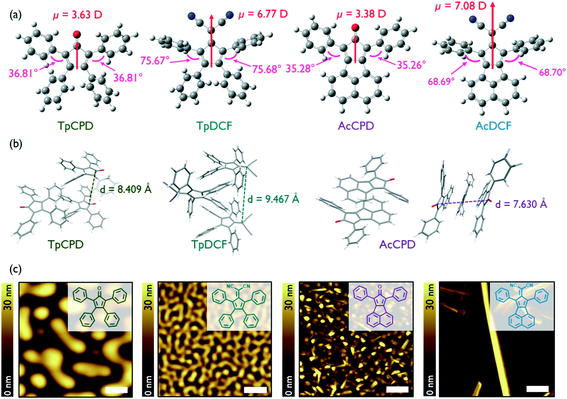 | ||
| Fig. 1 (a) Geometry-optimized (B3LYP/6-311G(2d,p)) structures of (from left) TpCPD, TpDCF, AcCPD, and AcDCF. Dipole moment values (red) and dihedral angles (pink) are indicated. (b) Crystal packing in TpCPD, TpDCF, and AcCPD obtained using Mercury software. (c) AFM height images of PVD grown samples with a deposition rate of 0.3 Å s−1 at RT. Scale bar is 1 μm. Chemical structures are illustrated in inset. More details about AFM images of AcDCF film including line profiles can be found in Fig. S1.† | ||
The reported crystal structures of TpCPD, TpDCF, and AcCPD13,14 revealed that these molecules packed in a head-to-tail fashion due to the influence of dipole–dipole interactions (Fig. 1b), which typically act to avoid accumulation of net nonzero dipoles in a given cluster.11 This observation suggested that dipole–dipole interactions are the major driving force for molecular arrangement in crystals of these dipolar molecules. The distance between two acenaphthene cores in AcCPD was 3.82 Å, whereas the smallest intermolecular distance in TpCPD and TpDCF was 4.20 and 4.73 Å, respectively. The relatively smaller intermolecular spacing in AcCPD confirmed that the extended π-systems found in AcCPD and AcDCF experience stronger van der Waals interactions as compared to TpCPD and TpDCF.
Next, we explored whether 1D growth of nanostructures of these four non-planar molecules could be affected using physical vapor deposition (PVD). Thin films of TpCPD, TpDCF, AcCPD, and AcDCF were grown on Si substrates. The deposition rate was maintained at 0.3 Å s−1 and the Si substrate was held constant at room temperature (RT). Intriguingly, crystalline nanostructures were readily observed in films of AcCPD and AcDCF, but not in films of TpCPD and TpDCF (Fig. 1c). The two-times larger dipole moment of TpDCF (6.77 D) versusTpCPD (3.63 D) did not observably induce crystalline order in vapor deposited thin films, thus indicating that dipole–dipole interactions were not influencing molecular self-assembly under the conditions investigated using PVD. In contrast, the presence of a larger π-system afforded 1D nanostructures, suggesting that van der Waals interactions were predominant during film growth. On silicon and ITO, 1D wires of AcCPD, on average, grew normal to the substrate plane, whereas wires of AcDCF grew parallel to the plane of the substrate. Remarkably, ultralong 1D wires (up to 65 μm, Fig. S2†) of AcDCF were observed using a straightforward PVD process without added surface treatments or sophisticated deposition algorithms. Besides the 1D structures, other morphologies were also observed in vapor deposited thin films of AcDCF, including polycrystalline regions and amorphous phases (Fig. 1c). We speculated that the larger dipole moment of DCF moieties, combined with the stronger van der Waals interactions of acenaphthene moieties, enriched the formation of 1D nanostructures during film growth.
Post-deposition annealing for six hours induced crystallization in all aforementioned films, including the previously-unstructured TpCPD and TpDCF films, and lead to the formation of close-packed crystalline structures on the Si substrate (Fig. S3 and S4†). Post-deposition annealing allows access to thermodynamically stable molecular assemblies or crystal phases. Annealing was not observed to change the d-spacing of the films of AcDCF (Fig. S5†). However, the AFM topographic images of the structures obtained after annealing were entirely different than those of the as-deposited thin films. This observation led us to hypothesize that the nanostructured AcDCF films obtained via PVD are a result of kinetically controlled self-assembly.
Controlling the kinetics of molecular assembly during thin film growth can influence the morphology, structure and degree of crystallinity of molecular solids.15,16 PVD, in particular, is a powerful deposition method that can be used to influence the self-assembly of small molecules into 1D nanostructures.4,17 Further, many deposition parameters, such as growth rate, source temperature, substrate temperature and chamber pressure, can be independently tuned to systematically investigate nucleation and crystal growth. Here, we used a PVD chamber with a temperature-controlled substrate stage held 10 inches away from the source crucible to vary the substrate temperature and growth rate (which was controlled by changing the source temperature). We maintained a chamber pressure between 10−7–10−6 Torr for all depositions.
Fig. 2a defines the associated rate constants that influence film growth and molecular assembly during PVD: the adsorption rate (kads), desorption rate (kdes), and surface diffusion rate (ksur) of molecules on a substrate.18 These kads and kdes values can be influenced by the substrate temperature and/or the source temperature (that is used to control growth rate), which imparts a particular kinetic energy (Ekin) to the source molecules before they reach the substrate. Further, the mobility of molecules and/or molecular clusters on the substrate surface (ksur) can be tuned by the substrate temperature. Typically, two modes of deposition can be accessed: equilibrium-limited and diffusion-limited. In an equilibrium-limited regime, either the kinetic energy (Ekin) of the molecular flux or the temperature of the substrate (Tsub) is sufficiently high to establish a dynamic equilibrium between adsorption and desorption at the interface (high kdes and ksur) that allows individual molecules and/or molecular clusters to sample multiple nucleation sites and conformations before final assembly into a thermodynamically-stable structure. In contrast, when either Ekin or Tsub decreases, the probability of condensation will increase and surface mobility will decrease (low kdes and ksur), thus leading to diffusion limited growth containing kinetically-trapped assemblies.
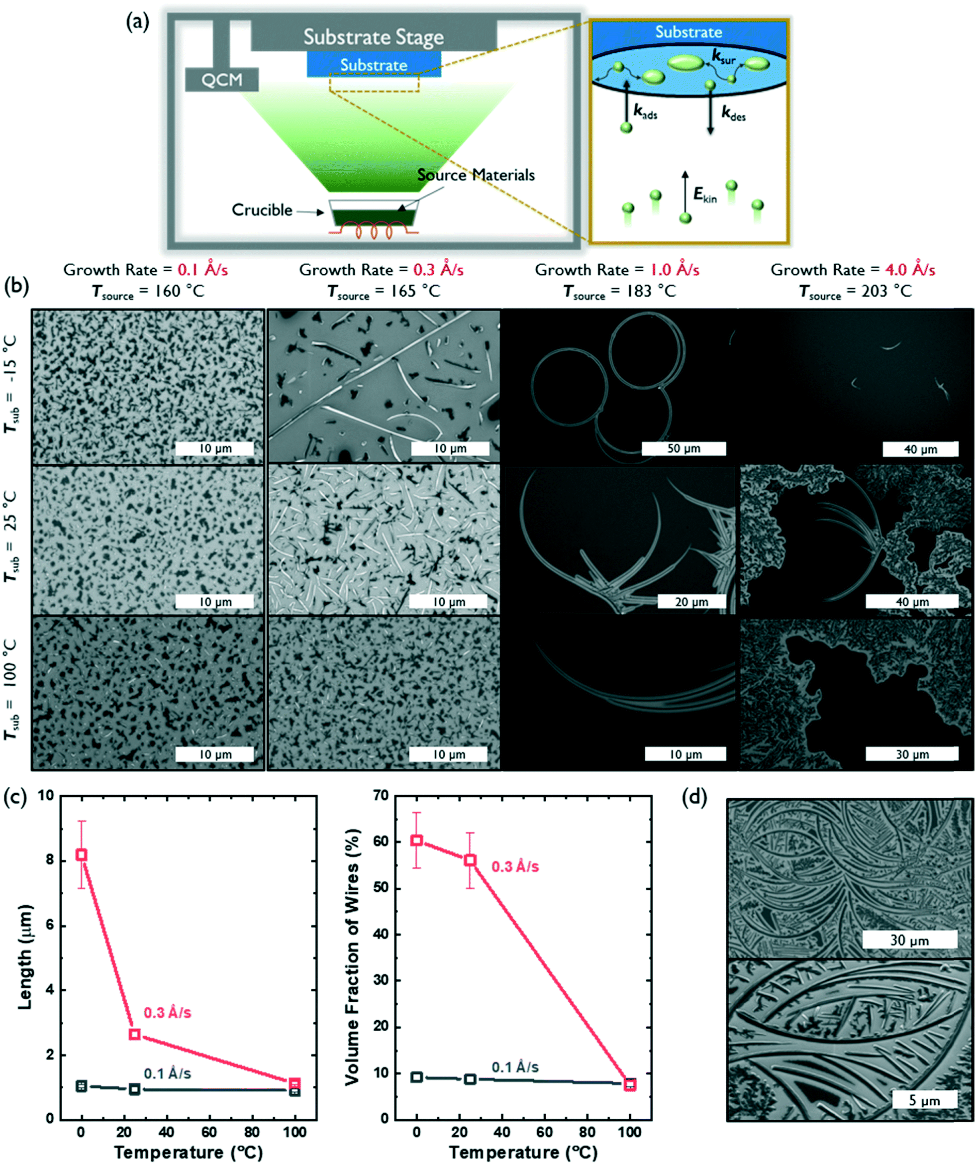 | ||
| Fig. 2 (a) Schematic illustration of the growth of AcDCF thin films via PVD. (b) SEM images of AcDCF samples created using PVD under various deposition conditions. (c) Length and volume fraction of the AcDCF wires as a function of Tsub. (d) SEM images of added AcDCF deposited onto substrates already containing curved nanostructures (1.0 Å s−1, Tsub = −15 °C). | ||
As expected, substrate temperature and growth rate had significant effects on the kinds of AcDCF nanostructures obtained via PVD (Fig. 2b). At an ultralow deposition rate of 0.1 Å s−1, AcDCF aggregated into small islands (which look dark in SEM images), independent of substrate stage temperature. The Ekin of the incoming molecular flux is very low at a deposition rate of 0.1 Å s−1, meaning that both kdes and ksur are very low, even at Tsub = 100 °C. Therefore, after isolated nucleation sites are established by the first few molecular monolayers, randomly-oriented crystal islands will be propagated.19
At a modest deposition rate of 0.3 Å s−1, 1D wires were obtained at low substrate temperatures but were not apparent at a high substrate temperature of 100 °C. This emphasizes the fine level of control afforded by PVD, particularly for creating various functional architectures out of non-centrosymmetric dipolar molecules. A Tsub of −15 °C evidently suppressed ksur and kdes enough to favour 1D growth. As Tsub increased, the density of wires decreased, likely due to an increased value of ksur, which should allow molecules and clusters to sample multiple nucleation sites and form randomly-oriented aggregates over time.
The average population density and length of AcDCF wires obtained under different deposition conditions were analysed over large areas (600 μm2) across 3 different depositions (Fig. 2c). AcDCF wires with a mean length of 8.19 μm were obtained with a deposition rate of 0.3 Å s−1 at Tsub = −15 °C. The mean length of the wires decreased to 2.65 μm and 1.13 μm at a Tsub of 25 °C and 100 °C, respectively. Additionally, the volume fraction of AcDCF nanowires also decreased from 60.4% to 6.6% as Tsub increased. Therefore, we concluded that a lower substrate temperature facilitated the elongation of AcDCF wires at low deposition rates (0.1–0.3 Å s−1).
We also investigated the effects of ramping up and ramping down the Tsub during the deposition while keeping the deposition rate constant at 0.1 Å s−1. We found that the volume fraction of 1D morphologies increased when the substrate was heating up as compared to when the substrate was cooled down during the deposition period (Fig. S6†). This is consistent with the decrease of nanowire populations with increasing Tsub as seen in Fig. 2c, indicating that the initial thermal environment of the PVD deposition plays a pivotal role in determining nucleation and growth of the organic crystals.
Interestingly, PVD of AcDCF at a deposition rate of 1 Å s−1 yielded micron-scale, curved wires—even producing complete rings. However, the volume fraction of these nanostructures was significantly lower than that of the straightforward 1D nanowires described earlier. The majority of the substrate surface was covered, instead, with clusters lacking long-range order. The circular and/or ring structures were obtained across multiple different depositions, specifically at a growth rate of 1 Å s−1. We suspect that such curved architectures can only be accessed due to the non-planar molecular structure of AcDCF (specifically, the twisted phenyl substituents in the 2,5-positions of the cyclopentadiene moiety) and likely grow from defects or dust particulates present on the substrate surface. Curved wires were also observed at a growth rate of 4 Å s−1, however, small clusters and polycrystalline domains were observed much more frequently. At a growth rate of 4.0 Å s−1 with Tsub = 100 °C, extensive desorption alongside adsorption at the substrate surface likely resulted in an equilibrium-limited deposition regime, which should yield polycrystalline films. Therefore, we concluded that we could only access crystalline 1D nanowires via kinetically controlled, diffusion-limited growth during the PVD process.
We also explored whether a self-templating effect could be effected when samples containing curved nanostructures were exposed to a second flux of AcDCF at a deposition rate of 1.0 Å s−1 at Tsub = −15 °C. When a 20 nm thick layer of AcDCF was deposited onto substrates containing curved nanowires, the overall density of wires increased, and new wires were observed to grow out of the original, curved structures (Fig. 2d). This observation confirmed that the curved nanostructures indeed encouraged incoming molecules to grow as 1D structures.
The charge transport properties of small molecular clusters versus 1D nanowires of AcDCF were studied using c-AFM, which enables measurement of local current density–voltage (J–V) curves and space charge limited currents (SCLC) with high spatial resolution (Fig. 3a).20 Samples are typically prepared on ITO. During the c-AFM measurement, a localized diode (either a Schottky or heterojunction diode) is created between the sample and the platinum-coated AFM tip. Charges can be injected from the ITO contact when a bias applied—holes, electrons or a mixture of both holes and electrons can be injected, depending on the band edge alignment of the sample relative to the work function of ITO—and collected at the platinum-coated AFM tip.
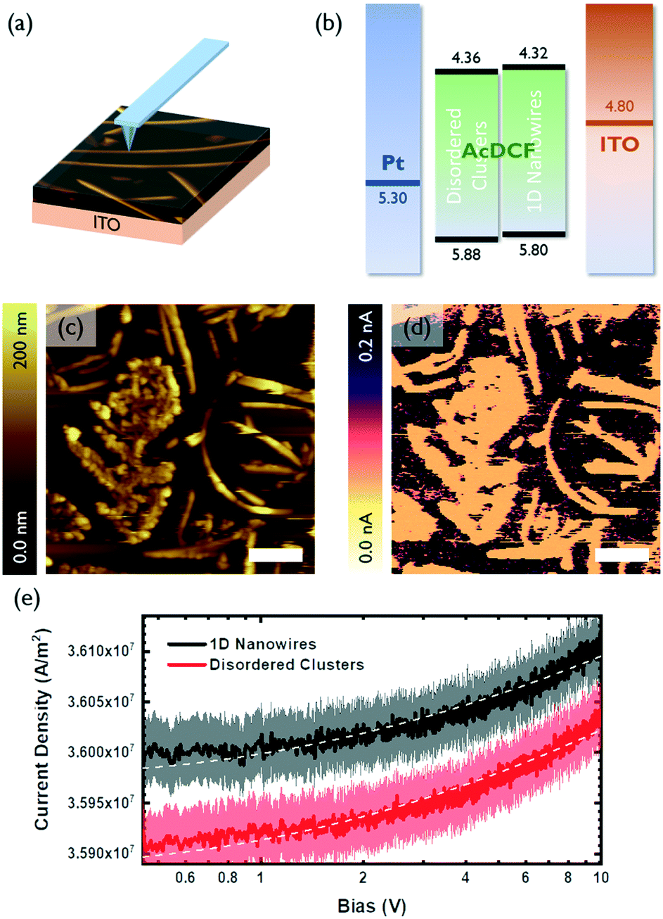 | ||
| Fig. 3 (a) Schematic illustration of c-AFM experiment procedure (b) energy levels of each layer of ITO/AcDCF/Pt architecture. (c) Representative AFM height image for c-AFM measurement. (d) Corresponding c-AFM image recorded simultaneously with the topography. Sample bias of 500 mV was applied during the measurement. (e) Local J–V curve obtained while locating the tip either on crystalline wires or non-crystalline regions. | ||
A representative area containing a polycrystalline region, randomly-oriented clusters and 1D wires of AcDCF was identified and scanned with a platinum-coated tip (Fig. 3c). The c-AFM image of this same area is shown in Fig. 3d and is consistent with the topographic image (Fig. 3c), confirming that c-AFM can reveal location specific J–V curves. Note that the AcDCF structures shown in Fig. 3c and d are resistive compared to the conductive substrate (ITO).
The local J–V curves for 1D wires and randomly-oriented AcDCF clusters were recorded over 20 different locations on a given substrate and averaged (Fig. 3e). The recorded current densities could be reasonably fit to a Mott–Gurney SCLC model (J ∝ V2) to extract charge mobilities.21Fig. 3b depicts the measured valence and conduction band edges of AcDCF (obtained by ultraviolet photoelectron spectroscopy and the optical band gap, respectively, Fig. S7 and S8†), and the known work functions of ITO and platinum. Both disordered clusters and 1D nanowires displayed low-lying band edges, meaning that large injection barriers were present for both electron and hole injection into the AcDCF layer at the ITO interface. Therefore, it was not clear whether these recorded J–V curves probed hole or electron mobility values in the AcDCF samples. Based on the relatively low extracted mobility values (ca. 10−7 cm2 V−1 s−1), we suspect that these measurements revealed hole mobilities in AcDCF samples, since CPDs and DCFs are known to be efficient electron transporters but poor hole transporters.22
Interestingly, even if we were indeed probing a minority charge carrier, the extracted mobilities were, on average, higher in 1D wires as compared to disordered clusters. Even though the thickness of the 1D wires (t ≈ 200 nm) was approximately two times higher than the thickness of the disordered regions (t < 100 nm), the crystalline wires supported higher current densities.
Experimental
Materials and methods
All molecules were synthesized and purified following reported procedures.14 Si and glass substrates were cleaned with 0.25% aqueous Micro90, deionized water, acetone, and 2-propanol in an ultrasonic bath for 10 min each in turn, followed by drying using N2 gas. We used a commercial PVD chamber (Angstrom Nexdep, USA) for the vapor phase deposition. The AcDCF powder was loaded in an alumina crucible, and then the crucible and the substrates were placed in thermal evaporation chamber. By heating the crucible to 180 °C, the molecules were deposited by thermal evaporation under high vacuum with a base pressure (<5 × 10⁻⁷ Torr). The deposition rate and the thickness of the films were monitored by a quartz crystal microbalance during the deposition. Substrate temperature was precisely controlled by Presto A30 temperature control system (Julabo, USA).Computation
DFT calculations were performed using Gaussian 09'. All ground state calculations were conducted using the B3LYP functional and a 6-311G(2d,p) basis set. Molecular geometries were optimized towards ground state, and then its global minimum was ascertained by vibrational frequency calculations.Characterization
The morphologies of the film surfaces were characterized using atomic force microscopy (Veeco Dimension 3100, NY, USA). Tapping mode AFM images were recorded using a PPP-NCHR cantilever (force constant = 42 N m−1, NanoWorld, Switzerland). Surface morphology images were obtained using scanning electron microscopy (Magellan 400, FEI, USA). We conducted c-AFM using Cypher ES AFM (Asylum Research, USA) with an ORCA current preamplifier mode. A Pt-coated HQ:NSC18 cantilever (force constant = 2.8 N m−1, Mikromasch, USA) enabled the measurement of electrical properties concomitant with topographical images. 500 mV was applied to the sample prepared on ITO substrate during the combined topography/c-AFM measurement. To obtain location-specific J–V curves for calculating charge carrier mobility, a Pt-coated AFM probe was slowly lowered onto the surface until the desired applied force was reached. Next, the voltage between the sample and the probe was swept between 0 V and 10 V and the resulting local current recorded, while maintaining a constant applied force. Local I/V characteristics were obtained over 20 different locations on five different samples. The contact area between the tip and the sample surface was determined using the reported radius of the tip (r = 30 nm). All AFM images were analysed using Gwyddion software.Conclusions
We examined the self-assembly of four small molecules (TpCPD, TpDCF, AcCPD, and AcDCF) possessing anisotropic, non-planar structures and large dipole moments, and established robust algorithms to control their molecular self-assembly via simple physical vapor deposition. Each molecule contained a central dipolar moiety, consisting of either a cyclopentadienone (CPD, ca. 3.5 D dipole moment) or dicyanofulvene (DCF, ca. 7.0 D dipole moment) core, surrounded by either four twisted phenyl (Tp) groups or a fused aromatic (acenaphthene, Ac) ring system. We found that only molecules containing the fused ring system formed 1D nanowires due to the stronger van der Waals associations of the long, planar acenaphthene moieties. We explored the kinetics of self-assembly of AcDCF during physical vapor deposition and concluded that diverse 1D morphologies, including both curved and linear nanostructures, were formed as a result of diffusion-limited growth. We found that low substrate temperatures (−15 °C) facilitated the elongation of AcDCF nanowires at low deposition rates (0.3–1.0 Å s−1) and were able to isolate a modest volume fraction (>60%) of long 1D nanowires (average length 8.19 μm, longest observed length 65 μm). Using conductive AFM, we show that 1D AcDCF wires support higher current densities relative to randomly-oriented clusters lacking long-range order.This work provides an experimental roadmap to create ordered 1D wires out of dipolar, non-centrosymmetric molecules, which are not typically known to form ordered structures. Using the knowledge born out of this effort, we can potentially create molecular solids with net non-zero dipole moments, which should display interesting light-matter interactions and ferroelectric properties.
Conflicts of interest
There are no conflicts to declare.Acknowledgements
This material is based upon work supported by the National Science Foundation under CBET 1706633. The authors thank Professor Stephen S. Nonnenmann in the Mechanical and Industrial Engineering Department at UMass Amherst for graciously granting access to his Cypher ES AFM and Zimu Zhou for valuable discussions on conductive AFM.Notes and references
- S. S. Dalal, D. M. Walters, I. Lyubimov, J. J. de Pablo and M. D. Ediger, Proc. Natl. Acad. Sci. U. S. A., 2015, 112, 4227–4232 CrossRef CAS PubMed.
- Y. S. Zhao, H. Fu, A. Peng, Y. Ma, Q. Liao and J. Yao, Acc. Chem. Res., 2009, 43, 409–418 CrossRef PubMed.
- G. R. Desiraju, J. Am. Chem. Soc., 2013, 135, 9952–9967 CrossRef CAS.
- Y. Guo, L. Xu, H. Liu, Y. Li, C. M. Che and Y. Li, Adv. Mater., 2015, 27, 985–1013 CrossRef CAS PubMed.
- Y. Xia, P. Yang, Y. Sun, Y. Wu, B. Mayers, B. Gates, Y. Yin, F. Kim and H. Yan, Adv. Mater., 2003, 15, 353–389 CrossRef CAS.
- F. S. Kim, G. Ren and S. A. Jenekhe, Chem. Mater., 2010, 23, 682–732 CrossRef.
- L. Zang, Y. Che and J. S. Moore, Acc. Chem. Res., 2008, 41, 1596–1608 CrossRef CAS PubMed.
- N. Wu, C. Wang, P. M. Slattum, Y. Zhang, X. Yang and L. Zang, ACS Energy Lett., 2016, 1, 906–912 CrossRef CAS.
- Y. Wu, H. Yan, M. Huang, B. Messer, J. H. Song and P. Yang, Chem. – Eur. J., 2002, 8, 1260–1268 CrossRef CAS.
- M. Owczarek, K. A. Hujsak, D. P. Ferris, A. Prokofjevs, I. Majerz, P. Szklarz, H. Zhang, A. A. Sarjeant, C. L. Stern and R. Jakubas, Nat. Commun., 2016, 7, 13108 CrossRef CAS PubMed.
- S. Lee, A. B. Mallik and D. C. Fredrickson, Cryst. Growth Des., 2004, 4, 279–290 CrossRef CAS.
- C. R. Martinez and B. L. Iverson, Chem. Sci., 2012, 3, 2191–2201 RSC.
- C. Alvarez-Toledano, O. Baldovino, G. Espinoza, R. A. Toscano, R. Gutiérrez-Pérez and O. García-Mellado, J. Organomet. Chem., 1997, 540, 41–49 CrossRef CAS.
- T. L. Andrew, J. R. Cox and T. M. Swager, Org. Lett., 2010, 12, 5302–5305 CrossRef CAS PubMed.
- J. Fraxedas, Adv. Mater., 2002, 14, 1603–1614 CrossRef CAS.
- C. D. Dimitrakopoulos and D. J. Mascaro, IBM J. Res. Dev., 2001, 45, 11–27 CAS.
- S. R. Forrest, Chem. Rev., 1997, 97, 1793–1896 CrossRef CAS PubMed.
- A. Kubono and R. Akiyama, J. Appl. Phys., 2005, 98, 093502 CrossRef.
- T. Wang, Y. Zhu and Q. Jiang, Chem. Sci., 2012, 3, 528–536 RSC.
- O. G. Reid, K. Munechika and D. S. Ginger, Nano Lett., 2008, 8, 1602–1609 CrossRef CAS.
- S. W. Button and J. M. Mativetsky, Appl. Phys. Lett., 2017, 111, 083302 CrossRef.
- C. Yang, S. Cho, R. C. Chiechi, W. Walker, N. E. Coates, D. Moses, A. J. Heeger and F. Wudl, J. Am. Chem. Soc., 2008, 130, 16524 CrossRef CAS.
Footnote |
| † Electronic supplementary information (ESI) available. See DOI: 10.1039/c9me00100j |
| This journal is © The Royal Society of Chemistry 2020 |