
 Open Access Article
 This Open Access Article is licensed under a
 Creative Commons Attribution 3.0 Unported Licence
Synthesis and characterization of Cu3SbS4 thin films grown by co-sputtering metal precursors and subsequent sulfurization†
A Azizur
Rahman
 *ab,
Emroj
Hossian
b,
Hetal
Vaishnav
b,
Jayesh B.
Parmar
b,
Arnab
Bhattacharya
*b and
Arun
Sarma
ac
*ab,
Emroj
Hossian
b,
Hetal
Vaishnav
b,
Jayesh B.
Parmar
b,
Arnab
Bhattacharya
*b and
Arun
Sarma
ac
aSchool of Advanced Sciences (SAS), Vellore Institute of Technology-Chennai campus, Chennai – 600127, Tamil Nadu, India
bDepartment of Condensed Matter Physics and Materials Science, Tata Institute of Fundamental Research, Colaba, Mumbai – 400005, India. E-mail: arnab@tifr.res.in
cNorth East Centre for Technology Application and Reach (NECTAR), Viswakarma Bhawan, Shaheed Jeet Singh Marg, New Delhi – 110016, India
First published on 31st October 2020
Abstract
Cu3SbS4 (famatinite) thin films were synthesized using a two-step process: Cu and Sb metals were first deposited by RF magnetron sputtering, followed by subsequent sulfurization. The influence of metal precursor ratio, sulfurization temperature and time on surface morphology, composition, and structural and optical properties was systematically investigated. X-ray diffraction and Raman analysis revealed the formation of Cu3SbS4 phase thin films, where the crystallinity and phase purity improve with sulfurization temperature. Synthesis at a process temperature of 425 °C gave phase-pure Cu3SbS4 thin film with uniform surface morphology, whereas secondary phases were formed at reaction temperatures lower than 400 °C. A temperature higher than 425 °C led to films with voids between the crystallites. The bandgap of the optimized films was measured to be 0.89 eV and 0.83 eV using UV-VIS-NIR spectroscopy and spectroscopic ellipsometry measurements, respectively. This suggests the potential use of Cu3SbS4 as an absorber layer for thin film solar cells.
Introduction
Copper antimony sulfide compounds commonly known as CAS materials are emerging semiconductors having potential applications in the field of photovoltaics,1–5 thermoelectricity,6,7 photo-electrochemical cells,8,9 supercapacitors10,11 and also as topological insulators.12 This material system is composed of the elements Cu, Sb and S which are relatively earth-abundant, low cost and of low toxicity. In addition to being earth-abundant, CAS thin films with good crystalline quality can be grown at much lower temperatures of ∼400 °C in contrast to well-established Cu–In–Ga–Se (CIGS) and Cu–Zn–Sn–S (CZTS) thin films.13 Hence, the CAS material system has recently attracted much attention, owing to its suitable optical and electrical properties for PV applications.13,14 CAS exist in four major crystal phases: CuSbS2 (chalcostibite), Cu3SbS3 (skinnerite), Cu3SbS4 (famatinite) and Cu12Sb4S13 (tetrahedrite). These semiconductor materials have bandgaps ranging from 0.5 to 2 eV, high absorption coefficient (α > 105 cm−1) and show p-type electrical conductivity15 which makes them ideal for photovoltaic applications. Among the four stable phases, CuSbS2 and Cu3SbS4 have been identified as potential candidates for solar cells. Among these two compounds CuSbS2 has been widely explored for PV applications.1–3,8 However, a recent theoretical investigation on the electronic structure of CuMCh2 (M = Sb, Bi; Ch = S, Se) predicts that CuSbS2 is unlikely to display the desired transport properties for use in solar cells as it has an indirect bandgap with low hole mobility.16 The same authors have preferred the use of the related materials like Cu3SbS3 and Cu3SbS4 provided they exhibit the requisite optical and transport properties. Similarly, Yu et al.,17 have done a computational study for identifying materials with a suitable solar absorption profile and identified CuSbS2 and Cu3SbS4 as worthy for investigation as solar cell materials.17 Additionally, they showed that Cu3SbS4 exhibits slightly higher spectroscopic limited maximum efficiency (SLME) of 25%, than CuSbS2 (22.9%).17 Thus, it is of utmost important to investigate the Cu3SbS4 phase in order to understand its suitability for solar applications and come up with scalable deposition methods.Cu3SbS4 phase has a reported direct optical bandgap in the range of 0.4 eV to 1 eV, high optical absorption coefficient (α > 104 cm−1) and p-type electrical conductivity.17–19 Most of the reported work on Cu3SbS4 is on materials only in the form of micro-structures20–22 and nanostructures23–26 synthesized by chemical routes. There are only few reports on the synthesis of Cu3SbS4 in thin film form.4,27–31 In spite of a variety of approaches available for the synthesis of Cu3SbS4, the presence of secondary phases co-existing with these materials and the non-uniform surface morphology still remains a challenge limiting practical use.31 Hence, studies on thin film growth of Cu3SbS4 are necessary to understand both fundamental growth mechanisms and the influence of various deposition parameters on the properties of these films. Among the different available techniques, RF magnetron sputtering is suitable for developing high-quality thin films with an advantage of scaling to large area; however, the processing of Cu3SbS4 through this route is still unexplored.
In this work, we report a two-stage process to develop phase-pure Cu3SbS4 thin films. As a first step the metal precursors (Cu and Sb) were co-sputtered by RF magnetron sputtering on a sapphire substrate. Later these sputtered films were sulfurized under vacuum at different temperatures. The synthesized materials were characterized by different experimental techniques, like GIXRD, Raman spectroscopy, SEM, TEM, UV-VIS-NIR spectroscopy and spectroscopic ellipsometry measurements. The influence of metal precursor ratio, sulfurization temperature and time on the structural, morphological, compositional, and optical properties are discussed, and the optimum conditions for the formation of phase-pure Cu3SbS4 thin films identified.
Method
The growth of Cu3SbS4 involves a two-step process. In the first step, metal precursors were co-sputtered onto the sapphire substrate, and then the samples were sulfurized in a vacuum-sealed quartz ampoule. RF magnetron sputtering was used to co-sputter copper and antimony metal precursors on the substrate. A schematic representation of the two-stage growth process is shown in ESI† (Fig. S1). The Cu and Sb targets (Testbourne Ltd, purity ∼99.99%) were fixed at a tilt angle of 45° and located at a mean distance of 7 cm from the substrate. The substrate was kept at a temperature of 200 °C for better film adhesivity and the substrate holder was rotated to ensure uniform deposition. A plasma of high purity (99.998%) Ar with a background pressure of ∼10−2 mbar and at a flow of 30 sccm was used during the co-sputtering process. Cu–Sb films of 250 nm thickness with different [Cu]/[Sb] ratios were sputtered on to the substrate and the elemental composition of the grown films was analyzed by EDX (energy dispersive X-ray spectroscopy) in a scanning electron microscope. A table showing the influence on RF power on the [Cu]/[Sb] ratio is shown in the ESI† (Table S1). The sputtered Cu–Sb thin films were then sealed in a quartz ampoule with excess sulfur (0.1 g). Prior to the sulfurization process, the quartz ampoule of 15 mm diameter and 30 cm length was cleaned with HF solution, thoroughly rinsed in deionized water and purged with high purity Ar gas to remove any traces of oxygen and other contaminants. The sputtered films along with sulfur were evacuated to a pressure of ∼6 × 10⁻⁵ mbar using a diffusion pump backed by rotary pump and sealed in the quartz ampoule. The vacuum-sealed precursors in quartz ampoule were heated in a single zone wire-wound tubular furnace at different temperatures ranging from 200 °C to 450 °C to complete the sulfurization process. The temperature of the furnace was ramped at a rate of 10 °C min−1, and then the samples were allowed to cool down to the ambient through natural heat-loss processes.The structural properties of the films were determined using a Rigaku Smartlab 9 kW rotating anode X-ray diffractometer at 1° incidence in a grazing incidence XRD (GIXRD) mode. Raman spectroscopy measurements were performed on the samples using a WITec Alpha 300R confocal Raman microscope. Detailed studies on microstructure and composition of the films were performed using a field emission scanning electron microscope (FESEM) operated at a voltage ranging from 5–20 kV (Zeiss Ultra FESEM). Optical transmission and reflection spectra were measured at normal incidence using a Cary 5000 spectrophotometer. Variable angle spectroscopic ellipsometry (VASE) were performed using an alpha-SE ellipsometer (J.A. Woollam Co.). High-resolution transmission electron microscopy (HRTEM) images and selected area electron diffraction (SAED) patterns were recorded using a 200 kV FEI Tecnai-20 system.
Result and discussion
X-ray diffraction
The Cu![[thin space (1/6-em)]](https://www.rsc.org/images/entities/char_2009.gif) :Sb ratio and sulfurization time were optimized previously in separate experiments (see ESI† for details). The conditions of these parameters—Cu:Sb metal ratio of 1:1 and dwell time of sulfurization process of 60 minutes—were kept constant for all temperature studies. Fig. 1 shows GIXRD patterns of CAS thin films sulfurized at temperatures varying from 200 °C to 450 °C. The GIXRD data demonstrate that the diffusion of sulfur vapor and formation of phases strongly depend on temperature. Sputtered Cu–Sb films sulfurized at higher temperatures like 450 °C and 425 °C exhibit prominent diffraction peaks at 2θ = 28.7°, 29.9°, 33.3°, 47.8°, 56.6° which can be attributed to (112), (103), (200), (204), (312) planes of Cu3SbS4 (famatinite) phase (JCPDS No. 00-035-0581). Peaks of other binary and ternary phases of these material system were not observed in this temperature range. Similarly, the GIXRD profile of films sulfurized at lower temperature range like 400 °C and 300 °C show diffraction peaks of binary Sb2S3 (stibnite) and CuS (covellite) phases in addition to the dominant Cu3SbS4 phase. The Sb2S3 and CuS peaks are denoted by ‘*’ and ‘▼’ symbols, respectively, in Fig. 1. For the films sulfurized at a much lower temperature of 200 °C, apart from the CuS, Sb2S3 phases, unreacted Sb metal (marked with a ‘°’ symbol) was observed as well. Decrease in sulfurization temperature leads to an increase in the percentage of CuS phase, which is also evident from the GIXRD profile. The formation of CuS phase and peaks from unreacted Sb might be due to inadequate thermal energy that make metal inter-diffusion and distribution of sulfur vapor difficult. The full width at half maximum (FWHM) for (112) plane of Cu3SbS4 decreased from 0.68° to 0.29°, indicating an improvement of crystalline quality with increase in temperature from 200 °C to 450 °C. The films were found to exhibit a tetragonal crystal structure with calculated lattice parameters a = 0.538 nm and c = 1.075 nm which are close to the reported lattice parameter values of the tetragonal Cu3SbS4 phase.30 The average particle size of these films, estimated from Scherrer's formula for (112) reflection, was found to increase from 12 nm to 30 nm with increasing temperature from 200 °C to 450 °C.
:Sb ratio and sulfurization time were optimized previously in separate experiments (see ESI† for details). The conditions of these parameters—Cu:Sb metal ratio of 1:1 and dwell time of sulfurization process of 60 minutes—were kept constant for all temperature studies. Fig. 1 shows GIXRD patterns of CAS thin films sulfurized at temperatures varying from 200 °C to 450 °C. The GIXRD data demonstrate that the diffusion of sulfur vapor and formation of phases strongly depend on temperature. Sputtered Cu–Sb films sulfurized at higher temperatures like 450 °C and 425 °C exhibit prominent diffraction peaks at 2θ = 28.7°, 29.9°, 33.3°, 47.8°, 56.6° which can be attributed to (112), (103), (200), (204), (312) planes of Cu3SbS4 (famatinite) phase (JCPDS No. 00-035-0581). Peaks of other binary and ternary phases of these material system were not observed in this temperature range. Similarly, the GIXRD profile of films sulfurized at lower temperature range like 400 °C and 300 °C show diffraction peaks of binary Sb2S3 (stibnite) and CuS (covellite) phases in addition to the dominant Cu3SbS4 phase. The Sb2S3 and CuS peaks are denoted by ‘*’ and ‘▼’ symbols, respectively, in Fig. 1. For the films sulfurized at a much lower temperature of 200 °C, apart from the CuS, Sb2S3 phases, unreacted Sb metal (marked with a ‘°’ symbol) was observed as well. Decrease in sulfurization temperature leads to an increase in the percentage of CuS phase, which is also evident from the GIXRD profile. The formation of CuS phase and peaks from unreacted Sb might be due to inadequate thermal energy that make metal inter-diffusion and distribution of sulfur vapor difficult. The full width at half maximum (FWHM) for (112) plane of Cu3SbS4 decreased from 0.68° to 0.29°, indicating an improvement of crystalline quality with increase in temperature from 200 °C to 450 °C. The films were found to exhibit a tetragonal crystal structure with calculated lattice parameters a = 0.538 nm and c = 1.075 nm which are close to the reported lattice parameter values of the tetragonal Cu3SbS4 phase.30 The average particle size of these films, estimated from Scherrer's formula for (112) reflection, was found to increase from 12 nm to 30 nm with increasing temperature from 200 °C to 450 °C.
 | ||
| Fig. 1 GIXRD patterns of samples sulfurized at temperatures of 200 °C to 450 °C; numbers indicate (hkl) indices of Cu3SbS4, secondary phases of metallic Sb, Sb2S3 and CuS are marked with different symbols. | ||
Raman spectroscopy
Raman spectroscopy measurements were performed on grown thin films using 532 nm laser excitation. The incident laser power was kept low (∼1 mW) in order to avoid structural modification or damage of the films as laser-induced surface changes have been observed in Cu based thin films at high optical flux levels.31,32 Raman scattering results for samples sulfurized at different temperatures are shown in Fig. 2. The spectra obtained for samples sulfurized in the temperature regime of 450 °C to 300 °C (Fig. 2(a)–(d)) have the main Raman modes located at 244, 273, 317 and 344 cm−1. These peaks are in good agreement with the characteristic modes of Cu3SbS4 phase as reported in literature and RUFF database (RRUFF ID: R11022).21,29 Further lower frequency peaks positioned at 71,90, 133, 143 cm−1 for Cu3SbS4 phase were observed as also recently reported.32 In addition to the above peaks, one mode observed at 496 cm−1 does not match any of the possible binary and ternary phases of the CAS system. The Raman spectra of samples sulfurized at temperatures higher than 400 °C show only the modes of dominant Cu3SbS4 phase. However, thin films sulfurized at a lower temperature of 300 °C show a mode at 472 cm−1 which is due to the presence of CuS phase. Raman modes of only CuS (472 cm−1) and Sb (113 and 152 cm−1) were observed in the sample sulfurized at 200 °C. The absence of CuS phase in Raman modes of the films sulfurized at temperatures above 400 °C is in corroboration with XRD results. | ||
| Fig. 2 (a) Raman spectra measured at room temperature at laser power ∼1 mW for thin films sulfurized at temperatures (a) 450 °C (b) 425 °C (c) 400 °C (d) 300 °C (e) 200 °C. | ||
Surface morphology
The surface morphology of these films was evaluated using FESEM imaging. Fig. 3 shows the significant effect of sulfurization temperature on the microstructure and surface morphology of films. Films sulfurized at 450 °C (Fig. 3(a)) show a discontinuous surface with lots of voids in between the grains. Decreasing the temperature to 425 °C (Fig. 3(b)) leads to the formation of continuous uniform layers with grains of size ranging from 100–500 nm. Further decrease in temperature leads to the formation of finer grains and promotes vertical morphological growth. Vertical flakes growth mode was observed for the samples sulfurized at 200 °C. EDX point measurements on such vertical flakes reveal the compositions of the CuS compound. A similar morphology has been previously seen in CuS films.33,34 SEM observations suggest that continuous films with uniform surface morphology can be obtained at a temperature of 425 °C. The cross-sectional FESEM image (Fig. 3(e)) of the film sulfurized at 425 °C shows a thickness of 250 nm. | ||
| Fig. 3 Scanning electron microscope images thin films sulfurized at temperatures (a) 450 °C (b) 425 °C (c) 400 °C (d) 300 °C (e) 200 °C (f) cross-sectional SEM image of sample sulfurized at 425 °C. | ||
Optical properties
The optical transmittance T(λ) and reflectance R(λ) spectra of Cu3SbS4 thin films sulfurized at different temperatures against wavelength are shown in Fig. 4. Transmittance and reflectance spectra show strong absorption region in the optical range of 1.3 to 1.5 μm, which can be attributed to the onset of the fundamental absorption edge of Cu3SbS4 thin films as reported in the literature.28,29 The weak absorption region in the range of 0.5 to 1.3 μm range arises due to the presence of the Sb2S3 impurity phase. The absorption edge seen in the range of 0.5 to 1.3 μm becomes more prominent for the samples grown at lower temperatures which is in corroboration with XRD and Raman spectroscopy results. Similarly, the reflectance spectra for samples sulfurized at lower temperatures like of 300 °C and 400 °C show peaks in the range of 0.8 to 1.2 μm range because of the presence of Sb2S3 phase. | ||
| Fig. 4 Transmittance and reflectance spectra of thin films sulfurized at different temperatures. | ||
Additional studies to determine the optical constants of the phase-pure Cu3SbS4 thin film grown at 425 °C were conducted using variable angle spectroscopic ellipsometry (VASE). The ellipsometry study was not performed on other samples because of the presence of impurity phases. The measurements were carried out in the spectral range of 250–1500 nm. The psi (Ψ) and delta (Δ) parameters were measured at 50°, 55°, 60°, 65° and 70° incidence angles (see ESI† for details). The roughness layer was modelled using a Bruggeman effective medium approximation. To obtain better fit results between the experimental and model data, mean squared error (MSE) value was kept below 10. The plots of real (n) and imaginary (k) part of the refractive index are shown in Fig. 5 for the film grown at 425 °C were the result of the best-fit Ψ and Δ between the experimental data and those generated by the model. Both the refractive index (n) and the extinction coefficient (k) show an abrupt increase in the range of 0.7 to 0.9 eV. This can be attributed to the optical transition near the fundamental bandgap Eg, which is in agreement with the values obtained by absorption spectroscopy. The refractive index has a peak value at 0.9 eV, beyond which the n value decreases gradually to 1.1 at 3.2 eV. The extinction coefficient (k) also shows a pronounced peak of 1.05 at 1.4 eV then the drops to 0.7 at 3.25 eV.
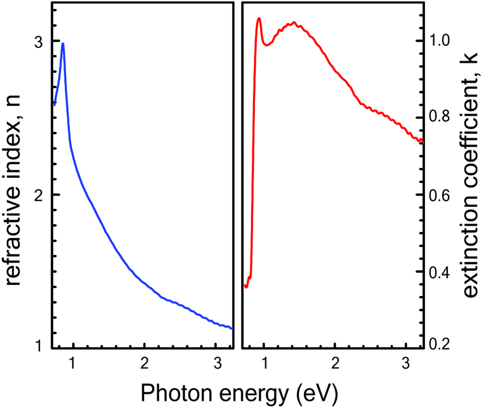 | ||
| Fig. 5 Refractive index (n) and extinction coefficient (k) as a function of photon energy for a phase-pure Cu3SbS4 thin film grown at 425 °C. | ||
The optical absorption coefficient (αλ) of the phase-pure Cu3SbS4 thin film was evaluated by both UV-VIS-NIR spectroscopy and ellipsometry techniques. In UV-VIS-NIR spectroscopy, the absorption coefficient was calculated using the equation, αλ = ln((1 − Rλ)2/Tλ)/t, using the value of Rλ and Tλ extracted from the transmittance and reflectance spectra of the sample. The thickness was determined from a cross-sectional SEM image, and estimated to be 250 nm. For the spectroscopic ellipsometry case, the absorption coefficient αλ was obtained by applying the formula αλ = 4πk/λ to the SE-derived k values. The optical bandgap of the phase-pure Cu3SbS4 thin film was then estimated by plotting (αhν)2versus hν (the Tauc plot) and taking the intercept. The (αhν)2versus hν plots estimated by both UV-VIS-NIR spectroscopy and ellipsometry for the optimized sample grown at 425 °C are shown in Fig. 6. (The Tauc plots of the other films sulfurized at different temperatures are shown in the ESI† as Fig. S5). The bandgap was determined to be 0.83 eV and 0.89 eV for ellipsometry and UV-VIS-NIR spectra respectively by linearly extrapolating (αhν)2vs. hν near the absorption edge of Tauc plot. These measurements show that the band edge of the film is appropriate for use as an absorber layer in thin-film solar cells.
 | ||
| Fig. 6 Tauc plot showing linearly extrapolated band edge obtained from spectroscopic ellipsometry and UV-VIS-NIR spectroscopy for samples sulfurized at a temperature of 425 °C. | ||
High resolution transmission electron spectroscopy
The synthesized films were further characterized by high-resolution transmission electron microscopy (HR-TEM). Fig. 7(a) shows an HRTEM image of Cu3SbS4 sample sulfurized at a temperature of 425 °C. Samples for TEM imaging were prepared by exfoliating the Cu3SbS4 films directly on to the TEM copper grid. The exfoliated layer exhibits averaged inter-planar distances of 0.53 nm and 0.49 nm, corresponding to the (002) and (101) planes. The representative selected area diffraction (SAED) pattern in Fig. 7(c) shows sharp diffraction spots, which can be indexed to the [111] zone axis. Similarly, Fig. 7(d) shows the HRTEM image of the vertical flakes which are sulfurized at a temperature of 200 °C, and exhibit an inter-planar distance of 0.32 nm and 0.16 nm which corresponds to CuS. SAED pattern of the samples also shows sharp diffraction spots which can be indexed to the [421] zone axis of CuS. | ||
| Fig. 7 High resolution TEM image of (a) Cu3SbS4 thin films sulfurized at 425 °C (b) CuS vertical flakes, sulfurized at 200 °C, (c) SAED pattern of Cu3SbS4 thin film (d) CuS flakes. | ||
Conclusion
Cu3SbS4 thin films were prepared by co-sputtering of metal precursors and subsequent sulfurization at temperatures from 200–450 °C. Significant improvement in structural and optical properties was seen at higher sulfurization temperatures. Uniform, phase-pure Cu3SbS4 films were obtained at 425 °C. These films had a tetragonal crystal structure with the lattice parameters a = 0.538 nm and c = 1.075 nm, and X-ray FWHM of 0.29° for the (112) plane. The direct optical band gap of these film was found to be in the range of 0.83–0.89 eV. The two-stage deposition process involving co-sputtering followed by sulfurization is scalable to large areas, and our results suggest that such films would be useful as an absorber layer in solar cells.Conflicts of interest
There are no conflicts to declare.Acknowledgements
We would like to acknowledge the support of Nilesh Kulkarni of TIFR, for assistance with X-ray diffraction measurements and the TIFR electron microscopy facility for TEM and SEM imaging. The work at TIFR was supported by internal grant 12P0165.Notes and references
- W. Septina, S. Ikeda, Y. Iga, T. Harada and M. Matsumura, Thin Solid Films, 2014, 550, 700–704 CrossRef CAS.
- S. Suehiro, K. Horita, M. Yuasa, T. Tanaka, K. Fujita, Y. Ishiwata, K. Shimanoe and T. Kida, Inorg. Chem., 2015, 54, 7840–7845 CrossRef CAS.
- Y. C. Choi, E. J. Yeom, T. K. Ahn and S. I. Seok, Angew. Chem., Int. Ed., 2015, 54, 4005–4009 CrossRef CAS.
- N. D. Franzer, N. R. Paudel, C. Xiao and Y. Yan, IEEE 40th Photovoltaic Specialist Conference (PVSC), 2014, pp. 2326–2328.
- G. H. Albuquerque, K. J. Kim, J. I. Lopez, A. Devaraj, S. Manandhar, Y. S. Liu, J. Guo, C. H. Chang and G. S. Herman, J. Mater. Chem. A, 2018, 6(18), 8682–8692 RSC.
- V. Kumar Gudelli, V. Kanchana, G. Vaitheeswaran, A. Svane and N. E. Christensen, J. Appl. Phys., 2013, 114, 223707 CrossRef.
- E. J. Skoug, J. D. Cain and D. T. Morelli, Appl. Phys. Lett., 2011, 98, 261911 CrossRef.
- C. Yan, Z. Su, E. Gu, T. Cao, J. Yang, J. Liu, F. Liu, Y. Lai, J. Li and Y. Liu, RSC Adv., 2012, 2, 10481–10484 RSC.
- M. Han, J. Jia and W. Wang, J. Alloys Compd., 2017, 705, 356–362 CrossRef CAS.
- V. K. Mariappan, K. Krishnamoorthy, P. Pazhamalai, S. Sahoo and S. J. Kim, Electrochim. Acta, 2018, 275, 110–118 CrossRef CAS.
- K. Ramasamy, R. K. Gupta, H. Sims, S. Palchoudhury, S. Ivanov and A. Gupta, J. Mater. Chem. A, 2015, 3, 13263–13274 RSC.
- Y. Wang, H. Lin, T. Das, M. Hasan and A. Bansil, New J. Phys., 2011, 13, 085017 CrossRef.
- B. Krishnan, S. Shaji and R. E. Ornelas, J. Mater. Sci.: Mater. Electron., 2015, 26, 4770–4781 CrossRef CAS.
- R. Ornelas-Acosta, S. Shaji, D. Avellaneda, G. Castillo, T. D. Roy and B. Krishnan, Mater. Res. Bull., 2015, 61, 215–225 CrossRef CAS.
- K. Ramasamy, H. Sims, W. H. Butler and A. Gupta, Chem. Mater., 2014, 26, 2891–2899 CrossRef CAS.
- D. J. Temple, A. B. Kehoe, J. P. Allen, G. W. Watson and D. O. Scanlon, J. Phys. Chem. C, 2012, 116, 7334–7340 CrossRef CAS.
- L. Yu, R. S. Kokenyesi, D. A. Keszler and A. Zunger, Adv. Energy Mater., 2013, 3, 43–48 CrossRef CAS.
- C. T. Crespo, J. Phys. Chem. C, 2016, 120, 7959–7965 CrossRef CAS.
- J. Van Embden, K. Latham, N. W. Duffy and Y. Tachibana, J. Am. Chem. Soc., 2013, 135, 11562–11571 CrossRef CAS.
- S. Blöβ and M. Jansen, Z. Naturforsch. B, 2003, 58, 1075–1078 Search PubMed.
- K. Aup-Ngoen, T. Thongtem and S. Thongtem, Mater. Lett., 2012, 66, 182–186 CrossRef CAS.
- G. Chen, W. Wang, J. Zhao, W. Yang, S. Chen, Z. Huang, R. Jian and H. Ruan, J. Alloys Compd., 2016, 679, 218–224 CrossRef CAS.
- J. Van Embden and Y. Tachibana, J. Mater. Chem., 2012, 22, 11466–11469 RSC.
- C. An, Y. Jin, K. Tang and Y. Qian, J. Mater. Chem., 2003, 13, 301–303 RSC.
- L. Shi, C. Wu, J. Li and J. Ding, J. Alloys Compd., 2017, 694, 132–135 CrossRef CAS.
- Q. Wang, J. Li and J. Li, Phys. Chem. Chem. Phys., 2018, 20, 1460–1475 RSC.
- M. Nair, Y. Pena, J. Campos, V. Garcia and P. Nair, J. Electrochem. Soc., 1998, 145, 2113–2120 CrossRef CAS.
- U. Chalapathi, B. Poornaprakash, H. Cui and S.-H. Park, Superlattices Microstruct., 2017, 111, 188–193 CrossRef CAS.
- U. Chalapathi, B. Poornaprakash and S.-H. Park, Ceram. Int., 2017, 43, 5229–5235 CrossRef CAS.
- A. Pfitzner and S. Reiser, Z. Kristallogr. - Cryst. Mater., 2002, 217, 51–54 CAS.
- P. Fernandes, A. Shongalova, A. da Cunha, J. Teixeira, J. Leitão, J. Cunha, S. Bose, P. Salomé and M. Correia, J. Alloys Compd., 2019, 797, 1359–1366 CrossRef CAS.
- A. A. Rahman, E. Hossain, H. Vaishnav, A. Bhattacharya and A. Sarma, Semicond. Sci. Technol., 2019, 34(10), 105026 CrossRef CAS.
- A. D. Savariraj, K. K. Viswanathan and K. Prabakar, Electrochim. Acta, 2014, 149, 364–369 CrossRef CAS.
- Y. Chen, C. Davoisne, J. M. Tarascon and C. Guéry, J. Mater. Chem., 2012, 22(12), 5295–5299 RSC.
Footnote |
| † Electronic supplementary information (ESI) available. See DOI: 10.1039/d0ma00574f |
| This journal is © The Royal Society of Chemistry 2020 |