
 Open Access Article
 This Open Access Article is licensed under a
 Creative Commons Attribution 3.0 Unported Licence
The tunable electric and magnetic properties of 2D MXenes and their potential applications
Vineeta
Shukla

Department of Physics, Indian Institute of Technology, Kharagpur-721302, India. E-mail: vineetashukla2@yahoo.com.in; vineeta@phy.iitkgp.ernet.in
First published on 29th September 2020
Abstract
The electrical and magnetic properties of 2D materials remain a subject of interest among researchers. After the discovery of the first 2D carbon material, the exfoliation of 2D MXenes has catalyzed their versatile applications in nanomedicine, spintronics, microwave absorption and energy storage systems. The pristine MXenes have a metallic character, but the presence of the terminal group makes it easy to tune their electrical and magnetic properties. This review paper is mainly focused on the electrical and magnetic property based applications such as cancer theranostics, spintronics, and shielding against electromagnetic pollution. This review paper will pave the way to designing the next generation of MXene based multifunctional materials with promising opportunities.
 Vineeta Shukla | Vineeta Shukla received degrees: Bachelor of Science, Bachelor of Education, Master of Science and Master of Philosophy from the C. S. J. M. University, Kanpur. She received two gold medals, the Sir C. V. Raman Commemoration Medal and the Kailashpat Singhania Medal for attaining the highest marks in Physics during her post-graduate degree. Currently, she is a doctoral student at the Indian Institute of Technology, Kharagpur, West Bengal, India. Her current scientific interests are focused on the characterization and energy applications of low dimensional materials. |
1 Introduction
The exfoliation of the first two dimensional (2D) material in 2004, known as graphene, opened up the door for searching for other 2D materials such as hexagonal boron nitride (h-BN), silicon and germanium counterparts, transition metal dichalcogenides (TMDs), transition metal carbides (TMCs)/nitrides (TMNs), etc.1,2 In this direction, various 2D materials such as silicene (2D allotrope of silicon),3–5 germanene (2D allotrope of germanium),6 molybdenum disulfide (2D TMD),7,8 phosphorene (2D black phosphorous),9–11 and many more have been studied so far.12–15 The 3D carbide and nitride counterparts that contain group IV–VI transition metals were discovered in the 20th century.16–18 These materials are known to possess good chemical stability, hardness, high thermal and high mechanical stability, and wear-resistant properties.19 The tremendous amount of research increased after 2011 when the first two-dimensional titanium carbide (Ti3C2Tx) was discovered by treating the MAX precursor Ti3AlC2 with hydrogen fluoride (HF) solution as the etchant.20,21 The 2D layered transition metal carbides, nitrides, and carbonitrides are named MXenes, and have the formula Mn+1Xn (n = 1–3) where n + 1 layers of M cover n layers of X.22 In general, MXenes have three formulae: M2X, M3X2, and M4X3 (M = early transition metal and X = C or N). In M2X, transition metal atoms form a honeycomb lattice, and another transition metal atom is found in the central of the honeycomb lattice. It shows an in-plane chemical arrangement, also known as i-MXene. However, M3X2 and M4X3 show out of plane chemical ordering, named o-MXene, in which the transition metal atoms are located in the perimeter layers and the other atoms occupy the central layers.23 i-MXenes can also be synthesized by substituting 1/3 foreign transition metal or rare-earth element M* for M in M2X, i.e. (M2/3M*1/3)2X.24 M* may be magnetic or nonmagnetic (NM), depending on our choice. On the other hand, o-MXenes are represented by the formula M2M*X2 or M2M*2X3. MXenes are generally synthesized by selective extraction of the desired atomic layers from their ternary layered precursors, i.e., MAX (Mn+1AXn) ceramics, known as MAX phases. The removal of the ‘A’ element by selective etching of Mn+1AXn, using HF, LiF/HCl, or NH4HF2 solution, results in a single sheet or a few sheets of the transition metal, named MXenes. In the formula Mn+1AXn, the M term indicates an early transition metal element such as Ti, Zr, and so on, while A refers to a group IIIA or IVA element such as Si, Al, and so on; on the other hand, the X term denotes C, N or both. MAX phases are known to possess inter-growth structures that comprise close-packed and alternative stacking of planar atomic layers and MX hexagonal layers. In this framework, the M–X and M–A bonds indicate the ionic/covalent and metallic characteristics. The covalent nature makes the M–X bond stronger than the M–A bond, making it facile to extract the A layer from the layered solid structure.22,25 Compared with the weak van der Waals forces in graphite and transition metal dichalcogenide interlayer interactions, the M–A bond of MXene can be considered to be relatively strong, which impedes the direct separation of MX layers from MAX phases through mechanical cleavage, dispersion, or by ultrasonication. A suitable chemical treatment helps us extract the A layer due to the different features and strengths of M–X and M–A bonds. Fortunately, one can obtain the MXene (Mn+1XnTx), where Tx indicates surface-terminating functional groups like fluorine (–F), hydroxyl (–OH), and oxygen (![[double bond, length as m-dash]](https://www.rsc.org/images/entities/char_e001.gif) O), by top-down and bottom-up approaches, and the MXene shows high chemical stability. The abundance of surface-terminating groups depends on the synthesis method, etchant solution, etc. Hydrogen bonding and van der Waals bonding are the two interactions that occur between the MXene layers. MXenes have a 2D lamellar structure and rich chemistry. MXenes demonstrate metallic character owing to the partially occupied d-shells of the transition metal atoms. The presence of abundant groups on their surfaces makes them hydrophilic, but increasing the number of groups causes the electrical conductivity to decrease. The activated metallic hydroxide sites, large surface to volume ratio, high melting point, high thermal conductivity, exceptional hardness, ultra-thinness, and good oxidation resistance make MXenes excellent materials in several fields, such as field-effect transistors,26 water purification,27 chemical sensors,28 biosensors,29 detection of volatile organic compounds,30 photo/electro-catalysis (e.g., photocatalytic hydrogen production,31 photocatalytic nitrogen fixation,32 CO2 reduction), energy conversion devices (including triboelectric nanogenerators, solar fuel generation and water splitting),33–36 capacitive desalination,37 biomedical applications,38 energy storage (including batteries and supercapacitors), spintronics, nano-electronics/optoelectronics, and topological applications.30,32,39,40 The lateral dimension of MXenes ranges from nanometers to micrometers, and the thickness is in the nanometer range.41 To date, 100 kinds of MXenes have been discovered through ab initio calculations, and more than 25 types of MXene have been obtained experimentally.22 Several research papers and reviews discussing photonics, optoelectronics, photothermal therapy, energy conversion, and storage applications of 2D MXene based materials have been reported.25,42–50 The present review paper discusses the electric and magnetic properties of MXene based composites and recent progress in MXene composites for biomedical applications, spintronics and protection from electromagnetic pollution.
O), by top-down and bottom-up approaches, and the MXene shows high chemical stability. The abundance of surface-terminating groups depends on the synthesis method, etchant solution, etc. Hydrogen bonding and van der Waals bonding are the two interactions that occur between the MXene layers. MXenes have a 2D lamellar structure and rich chemistry. MXenes demonstrate metallic character owing to the partially occupied d-shells of the transition metal atoms. The presence of abundant groups on their surfaces makes them hydrophilic, but increasing the number of groups causes the electrical conductivity to decrease. The activated metallic hydroxide sites, large surface to volume ratio, high melting point, high thermal conductivity, exceptional hardness, ultra-thinness, and good oxidation resistance make MXenes excellent materials in several fields, such as field-effect transistors,26 water purification,27 chemical sensors,28 biosensors,29 detection of volatile organic compounds,30 photo/electro-catalysis (e.g., photocatalytic hydrogen production,31 photocatalytic nitrogen fixation,32 CO2 reduction), energy conversion devices (including triboelectric nanogenerators, solar fuel generation and water splitting),33–36 capacitive desalination,37 biomedical applications,38 energy storage (including batteries and supercapacitors), spintronics, nano-electronics/optoelectronics, and topological applications.30,32,39,40 The lateral dimension of MXenes ranges from nanometers to micrometers, and the thickness is in the nanometer range.41 To date, 100 kinds of MXenes have been discovered through ab initio calculations, and more than 25 types of MXene have been obtained experimentally.22 Several research papers and reviews discussing photonics, optoelectronics, photothermal therapy, energy conversion, and storage applications of 2D MXene based materials have been reported.25,42–50 The present review paper discusses the electric and magnetic properties of MXene based composites and recent progress in MXene composites for biomedical applications, spintronics and protection from electromagnetic pollution.
2 Advantages and disadvantages of MXenes in comparison with other 2D materials
Graphene, hexagonal boron nitride, transition metal dichalcogenides, etc. have been comprehensively studied due to their intriguing properties such as high electrical conductivity, low density, large surface area, etc.51,52 Compared with these 2D materials, MXenes have some advantages due to their tunable electric and magnetic properties, e.g., pure 2D graphene has excellent electrical conductivity but demonstrates poor magnetic properties, and is not suitable for electromagnetic interference (EMI) shielding applications which require moderate conductivity and magnetic dipoles to interact with electromagnetic (EM) waves. The hydrophobic nature and high-cost synthesis of carbon allotrope (such as carbon nanotubes (CNTs), carbon nanofibres (CNFs)) based composites lower the extent of their use for EMI shielding materials.53,54 On the other hand, molybdenum disulfide (MoS2) is a 2D transition metal dichalcogenide with a layered structure. The MoS2 material is a semiconductor (bandgap of ∼1.2 eV) with a parabolic energy dispersion relation. The bandgap can be tuned by the quantum confinement effect resulting from different surface morphologies; hence MoS2 is a candidate for EMI shielding applications.55,56 As compared to 2D graphene, pure MoS2 has lower electron conductivity and lower permittivity due to poor charge transfer. A further problem with TMDs is that stacking of individual vertical layers of MoS2 takes place due to weak van der Waals forces, which may cause impedance mismatching between the EM waves and the shielding material.57 Fortunately, MXenes have tunable conductivity ranging from metallic to semiconductor, cost-effective synthesis, and hydrophilicity. Many MXenes possess an intrinsic magnetic moment, thus presenting applicability for EMI shielding and microwave absorption applications. However, an excess of terminal groups (oxygen and fluorine-containing) in the MXene sheet can cause collapse of the indispensable layer structure or heaping of layers in the lamellar MXene. The layered structure may hinder the creation of spaces, ranging from nano to submicron-scale, within the MXene that can alter its electric and magnetic characteristics, thus adversely affecting the EMI performance of MXene based composites. This is the drawback of MXenes, and can be improved through the synergistic effect between MXenes and conducting and/or magnetic materials, including metallic materials or ceramics, conducting polymers, and carbon allotropes.Pristine 2D graphene is a zero bandgap semimetal. While reduced graphene oxide and graphene oxide are a semiconductor and an insulator, respectively.54 2D TMDs show semiconducting behavior. The beauty of MXenes is their tunable electric properties that establish MXenes sometimes as metals, semiconductors, superconductors, topological insulators, and, most importantly, half-metals.58–61 The half-metallicity in MXenes can be tuned by controlling the terminal group, doping, or applying an electric field and strain. The half-metallic character of MXenes indicates future opportunities in the area of spintronics.62
For gas and liquid separation, GO analog based membranes have been established as promising membrane materials owing to their unique 2D structure. Nevertheless, the small interlayer spacing of GO analogs causes relatively low flux under pressure.63 For instance, Huang et al. reported ∼1702 g m−2 h−1 flux for the GO membrane under vacuum conditions.64 Disruption of hydrogen bonds can occur within the membrane due to the hydration effect that can increase the layer spacing of the GO membrane, causing instability in separation performance. In comparison to GO membranes, MXene based materials have good thermal resistance, and superior structural and chemical stabilities. By introducing nanochannels among the layers of the MXene membrane, ultra-fast water flux can be achieved.27 With extremely short transport pathway and large amounts of nanochannels, the MXene membrane showed high water permeance and rejection rate (i.e., 1000 L m−2 h−1 and 90%, respectively). GO membranes are almost impermeable to organic solvents, but MXene membranes are permeable to both water and organic solvents.65 The loose lamellar MXene structure endows a proper flow channel for the solution, leading to the high flux. Thus, it is anticipated that MXenes have excellent potential in membrane technology. However, MXenes show less rejection of dye molecules, and this is the main problem which could be improved by combining other materials with MXenes.65,66
Energy storage and conversion have become vital issues in present times. Batteries, such as lithium ion, sodium ion and potassium ion batteries, and supercapacitors are popular electrochemical energy storage (EES) systems. Their common features such as long cycle life, high energy density, power density, and environmental mildness show the superiority of fast-growing energy storage devices.67 The benefits of 2D graphene or 1D carbon nanotube (CNT) based electrode materials are their large surface area, high conductivity, and high mechanical stability. Furthermore, carbon based materials store charge by adsorption of ions in the electrolyte, and thus liberate low energy densities. In this context, pseudo-capacitive materials (i.e., transition metal oxides (RuO2, MnO2), conducting polymers, TMDs) are used to achieve high power densities. Metal oxides/hydroxides suffer from poor electrical conductivity which results in modest cycling performance and power densities. Subsequently, 2D TMDs such as MoSe2 nanosheets tend to agglomerate because of high surface energy. Also, 2D TMDs (i.e., MoSe2) have higher resistance when used as electrode materials, and agglomeration causes rapid capacity fading that prevents their large scale use in EES. The advantage of MXenes as electrode materials for EES is their unique structure that has a transition metal oxide-like surface with an inner conductive transition metal carbide layer that provides active sites for fast redox reactions and enables sufficient electron transportation. Although chemically synthesized MXenes contain terminal surface groups, several MXenes still exhibit metallic conductivity (e.g., Ti3C2Tx), which favors fast faradaic reactions, giving rise to superior charge storage properties (i.e., pseudocapacitance).68 Unfortunately, the stacked MXene nano-structure has the disadvantages of low capacitance and poor rate capability that lower its broad applicability in EES systems, but can be improved through the synergistic effects of MXenes and other materials, a controlled synthesis procedure, etc. For instance, the use of a group terminated MXene substrate with MoS2 nanosheets suppresses the aggregation of nanosheets, thus improving the conductivity of TMD/MXene based electrode materials.69 Therefore, it is concluded that the unique properties of MXenes make them excellent materials compared with other 2D materials.
The major drawbacks of MXenes are their standard synthesis procedures and the lack of understanding of their surface chemistry which requires more study and provides a great opportunity for future technological applications. The chemical etching and delamination method leaves terminal functional groups and defects on the surface of MXenes while the number of layers can change their physical properties. Thus, controllable surface termination needs to be explored. On the other hand, bottom-up approaches hinder their large scale production and lead to substrate dependent properties that limit their wide applicability in potential applications. Therefore, optimization of the MXene synthesis and understanding of the surface functionalities of MXenes have become important. For instance, pristine MXenes show poor photon absorption and high charge carrier recombination rate in photocatalytic applications. Similarly, pristine MXenes have high conductivity, and some of them are nonmagnetic which hinders their use in EMI shielding. In this context, understanding the surface chemistry of MXenes offers plenty of possibilities for their use in efficient EMI shielding, photocatalysis, and many more applications, and may be helpful in developing smart MXene based devices in the near future.70–73
3 Two popular synthesis methods for MXenes
Various synthesis processes, including chemical vapor deposition, physical vapor deposition, plasma-enhanced pulsed laser deposition,74 and the chemical etching method, are used to synthesize MXenes.75 Among the different bottom-up approaches, the chemical vapor deposition method has been reported in the literature to make surface-termination-free MXenes. Nevertheless, bottom-up approaches are less explored for synthesizing MXenes because of the formation of non-2D carbides with 2D MXenes.76 The selective chemical etching method (top-down method) is the most popular method among researchers due to ease of synthesis, easy handling in the laboratory, and low-cost preparation. However, the etching method's major drawback is the use of harmful acids which reduces its popularity to some extent. The synthesis conditions such as etching conditions, reaction time, the aggressiveness of the etchant, type of transition metal, and etchant greatly influence the surface terminations, morphology, and structural defects in the MXenes. For instance, the etching conditions can tune the morphology of MXenes. Accordion-like particles were observed when concentrated HF was used and could not be found under milder etching conditions. Moreover, a higher concentration of etchant, e.g., HF, gives rise to higher fluorine (F) content on the surfaces of MXenes. Meanwhile, the use of an aggressive etchant enhances the structural defects in MXenes. The surface terminations depend on the transition metal. Furthermore, the number of layers in MXenes is also influenced by the factors mentioned above. Thus the intrinsic properties of 2D MXenes cannot be fully explored by chemical modification. In this direction, many researchers have made an effort to make MXenes environmentally friendly by using less harmful eco-friendly chemicals that may pave the way for facile synthesis of MXenes and open the door for future opportunities. Moreover, to date many MXenes cannot be obtained through the following synthesis methods. Thus different and new synthesis methods for the preparation of undiscovered MXenes need to be explored. The two most popular techniques are discussed in the following sections.3.1 Top-down approach
Some popular top-down approaches are lithography, chemical etching, etc. Micro and/or nano-sized structures can be achieved through these methods by reducing the bulk material powder, making it smaller, and removing the remaining bulk part from it. Among the various top-down methods, MXenes are prepared by selective etching methods, as explained in the following section.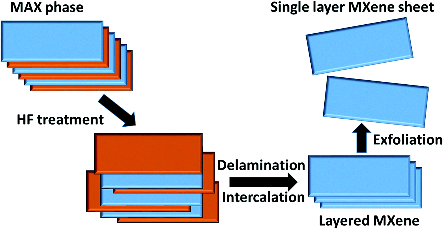 | ||
| Fig. 1 Pictorial representation of the preparation of an MXene nanosheet through the etching method by use of HF solution. | ||
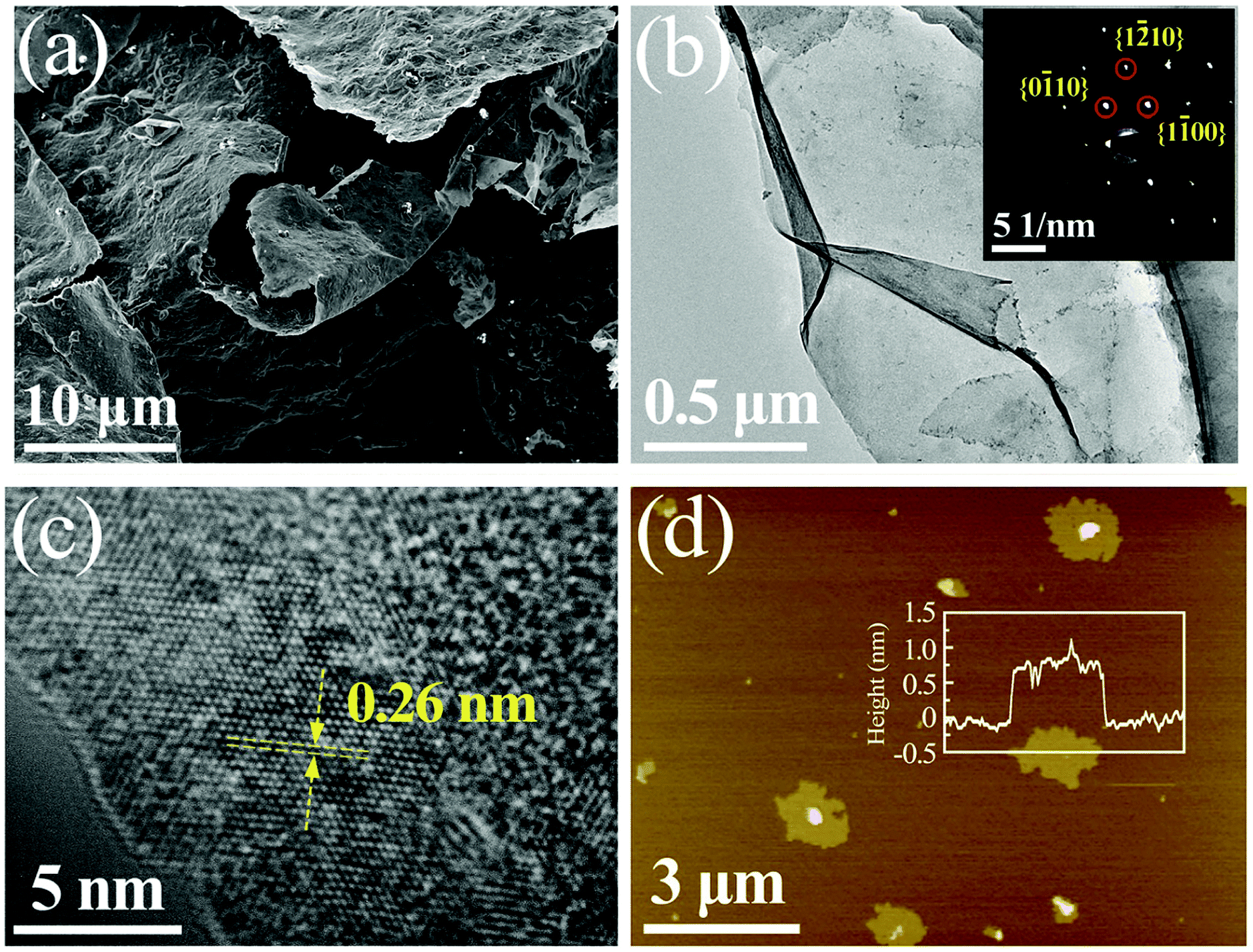 | ||
| Fig. 2 (a) SEM image of MXene, (b) TEM image of MXene (inset shows the SAED pattern), (c) high-resolution TEM image from (b), (d) AFMc image of MXene with height profile depicted in the inset,84 reproduced by permission of Elsevier. | ||
3.2 Bottom-up approach
The chemical etching method (top-down method) is facile and is the most popular technique for mass production of MXenes. However, the use of an acid solution such as LiF/HCl or HF leaves various functional groups and defects on the surface of MXenes. Additionally, the sonication process for delaminating MXene layers introduces more defects and makes them smaller. The bottom-up approach is used as an alternative chemical method to tackle the above problem and make the MXenes defect-free. Some bottom-up methods include the template method, chemical vapor deposition, and plasma enhanced pulsed laser deposition, which allows the study of a system's intrinsic properties. Among them all, chemical vapor deposition is widely studied for preparing MXenes and is explained in detail in the following section.4 Electrical and magnetic properties
The electrical and magnetic properties in low dimensions have always attracted the attention of condensed matter physicists due to the richness of the physics. Most MXenes are metallic due to the partially occupied d-shells of the transition metal atoms and their unusual coordination with neighboring atoms. The electrical properties of MXenes are anisotropic because the metallic conductivity differs moderately along the c- and a-axes but remains in the same order of magnitude. Interestingly, most 2D materials are nonmagnetic.54 At finite temperatures, the Mermin–Wagner theorem prohibits long-range ordered magnetic interactions in 2D systems with continuous spin symmetry.93 Nevertheless, tunable magnetic properties in 2D materials are in high demand due to their applicability in quantum computation, nanomedicine, logic and memory operations, spintronics, magnetic sensors, etc.94–98 Thus, the magnetic anisotropy property of magnetic 2D materials can be realized to explore practically important 2D materials. Upon doping or applying an electric field, the long-range ordering is maintained by modulating the exchange interactions and magnetic anisotropy which limits the magnetism in 2D materials. Different experimental approaches have been reported to induce magnetism in 2D materials.99–102 Apart from graphene with p-orbitals, some TMCs and TMNs with partially filled d-orbitals possess an intrinsic magnetic moment. Khazaei and coworkers obtained ferromagnetic ground states in Cr2C and Cr2N MXenes.103 Meanwhile, Cr3C2, Ti2C, Ti2N, and Ta3C2 are also predicted to be ferromagnetic.104–106 However Ti3C2, Mn2C and Ti3N2 showed antiferromagnetic (AFM) nature. The benefit of using MXenes is their intrinsic magnetic properties obtained by the selective choice of transition metal atoms, which give the d-electrons freedom in the 2D system. Additionally, transition metal carbides/nitrides consist of carbon or nitrogen layers with the transition metal layers, which also contribute to the magnetism and the conduction process, e.g., in transition metal carbides, the carbon layers of MXenes show similar characteristics to graphene, giving rise to high electrical conductivity. Thus, the physical properties of MXenes are highly influenced by the coordination of the d-electrons of the transition metals with neighboring atoms and the number of d-electrons. In this direction, Kumar et al. studied the transition metal nitride MXenes M2NT2 where M = Ti, V, Cr, Mn, and T = F, OH, O and suggested that N in nitride MXenes provides an extra electron with respect to carbide MXenes that causes an excess in the density of states around the Fermi level. This excess density of states not only results in higher conductivities but also stabilizes the ferromagnetic ground states following the Stoner criterion.107,108 Subsequently, surface terminating groups such as F, OH, or O groups confer additional freedom, which can be used to obtain the desired magnetic properties of MXenes. Hu and coworkers predicted the 2D Mn2C monolayer as an antiferromagnetic metal. Nevertheless, the functionalized Mn2CF2 MXene showed ferromagnetic half-metal character with a high Curie temperature of 520 K and a wide half-metallic gap of 0.9 eV.109 Interestingly, He and coworkers predicted that the Mn2C MXene functionalized with F−, Cl−, and OH− retains the ferromagnetic (FM) ground state upon functionalization. While O and H functionalized Mn2C became nonmagnetic upon functionalization.110 In MXenes, the strength of the bonding between the metal cation and the ligand anion is given qualitatively by crystal field theory which describes the breaking of orbital degeneracy owing to the ligands in octahedral or tetrahedral transition metal complexes. Octahedral complexes are accepted to be energetically more favorable than tetrahedral symmetry in MXenes. TMDs also possess octahedral symmetry in which non-bonding states are located within the gap between the bonding (σ) and antibonding (σ*) bands of the M–X bonds according to crystal field theory.111 Similarly, the non-bonding states of MXenes lie between the bonding (σ) and antibonding (σ*) states of the M–X and M–T bonds. The crystal field causes further splitting of the non-bonding states into low energy (dxy, dyz, and dxz) t2g states and high energy (dx2−y2 and dz2) eg states. It is predicted by scientists that the number of available electrons in the non-bonding states and the way of filling non-bonding d-bands decide the electronic and magnetic properties of MXenes, similar to TMDs. For example, partially filled orbitals indicate metallic conductivity while fully occupied orbitals show semiconducting behavior. According to the Goodenough–Kanamori rule, if the half-filled orbitals of two cations and the p-orbital of a ligand overlap, the ligand-mediated superexchange interactions result in AFM behaviour.112 Assuming cations with partially occupied or empty orbitals, then the magnetic ordering can be FM or AFM and is further decided by the direct exchange interaction between metal ions/groups and ligands. On the other hand, the double-exchange interaction gives rise to ferromagnetic ordering if maximum hopping between partially occupied d-orbitals takes place without flipping of their spin directions.113 For the previously mentioned M2NT2 MXenes where M = Ti, V, Cr, Mn, and T = F, OH, O, Kumar et al. predicted itinerant character for the electrons in the oxygen-terminated nitride MXenes, while the fluorine-terminated nitride MXenes showed localized behavior of the electrons. Fortunately, the itinerant character favors FM ordering due to the dominant double-exchange interaction. However, double-exchange interactions are weak for localized electrons, and so the superexchange interactions describe the magnetic ground state of the fluorine-terminated nitride MXenes. Fig. 3a–f show the density of states and band structure plots for the spin up and spin down states of Mn2NF2, Mn2NO2, and Mn2N(OH)2. The density of states of Mn2NT2 (T = F, O, OH) shows large exchange splitting for the minority spin, indicating the robust half-metallic nature. Furthermore, delocalized fluorine p-states are observed below the Fermi level. In the band structure plots, one spin channel shows metallic behavior while the other spin channel shows insulating behavior with a large band gap. It is proposed that a strong local magnetic exchange field is generated by a large local magnetic moment. Consequently, the band gap opens due to lifting of the minority spin states above the Fermi energy.107 Frey and coworkers studied M2NTx MXenes, where M refers to Ti, Cr, and Mn. They suggested that appropriate modification of the surface termination and transition metal in M2NTx can provide the desired spin structure and tunable magneto-crystalline anisotropy. The investigation revealed that the spin symmetry could be manipulated by spin–orbit coupling, which helps tune the magnetic interaction from X–Y ferromagnetism to Ising ferromagnetism.114 Yoon et al. used a low-temperature solution chemical synthesis method to prepare the Ti3C2 MXene. Since the parent MAX phases of the Ti3C2 MXene are Pauli paramagnets, they expected to obtain a strong paramagnetic signal from the chemically reduced Ti3C2Tx MXene. Consequently, the as prepared Ti3C2Tx MXene showed Pauli paramagnetic behaviour.115 Recently, Babar et al. observed a magnetic phase transition from the paramagnetic Nb2AlC–MAX to the superconductor-like diamagnetic Nb2C–MXene.116 The electrical and magnetic properties of MXenes depend on various factors which are explained in the following sections.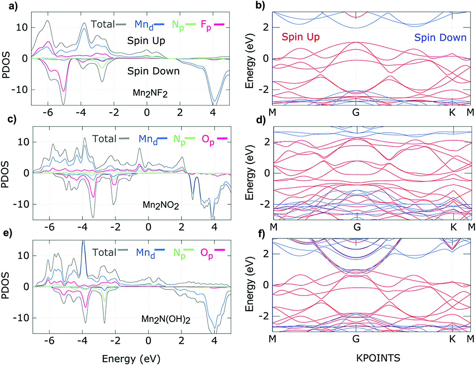 | ||
| Fig. 3 Density of states of (a) Mn2NF2, (c) Mn2NO2, and (e) Mn2N(OH)2, and band structure plots for (b) Mn2NF2, (d) Mn2NO2, and (f) Mn2N(OH)2 (red and blue solid lines represent majority and minority spins, respectively),107 reproduced by permission of the American Chemical Society. | ||
4.1 Asymmetric functionalization
Sometimes the surface is saturated with functional groups during the synthesis of MXenes. As a result, the ground states changes from FM to AFM or nonmagnetic (NM) states. To overcome the problem, asymmetric decoration on the MXene surface can be done. Therefore, magnetic properties of MXenes can also be achieved by asymmetric/non-centrosymmetric functionalization with F, O, etc. groups. With asymmetric surface functionalization, Frey and coworkers obtained magnetic ordering in Janus M2XOxF2x, where X is C, N, and x = 0.5, 1, or 1.5. The magnetic ground states in these nonmagnetic or weakly magnetic structures are induced by the local structure and chemical disorder with respect to the pristine form. Observations revealed that Janus Cr2C, V2C, and Ti2C were stabilized in the AFM state while mixed termination-induced anisotropy gave rise to Ising ferromagnetism for Janus Mn2N.117 Zheng et al. investigated the Ti2C MXene by asymmetric surface decoration. The asymmetrical adsorption of negative ions or metal atoms causes the Ti atoms to exhibit different valence states, Ti4+ and Ti+, which favors a FM ground state.61 It is anticipated that asymmetric functionalization of unexplored new MXenes may reveal some interesting magnetic features.4.2 Surface-passivated MXenes
Theoretical calculations predict that surface terminations on the MXenes greatly influence the density of states (DOS) at the Fermi level and, therefore, the magnetic properties and electronic conductivity. Si and coworkers predicted half-metallic ferromagnetism in a graphene-like 2D Cr2C crystal and observed a surface functionalization induced metal–insulator transition in the Cr2C configuration.104 The Ti3C2 monolayer MXene is also found to be a magnetic metal, but the –F or –OH group containing Ti3C2F2 and Ti3C2(OH)2 exhibit small band gaps and act as semiconductors.118 The Cr2CT2 MXene where T = F, (OH), Cr2NT2 where T = F, (OH), and O terminated MXenes exhibit ferromagnetic ground states.103 Hart and coworkers studied the electronic properties of MXenes through termination and intercalation. They found that transitions between metallic and semiconductor behavior were induced through intercalation, while de-functionalization of the surface of the MXenes gave rise to increased electronic conductivity.62 Similarly, Wang and colleagues found an enhanced electrical conductivity of 2140 S cm−1 for Ti3C2 MXene nanosheets treated at 600 °C. This is ascribed to the fact that the post-treatment processes effectively remove the functional groups on the surface of Ti3C2 which makes the electrical conductivity three times higher than that of untreated Ti3C2 nanosheets.119 Li et al. studied the effect of surface-functionalization (denoted by X = O, F and OH) in the (V2/3Zr1/3)2CX2 system, and (V2/3Zr1/3)2CO2 MXene presented with a half-semiconductor nature and ferromagnetism at a Curie temperature of 270 K.120 Li and coworkers obtained ferrimagnetic half-metallicity with a gap of 0.47 eV in the 2D Mo3N2F2 MXene with a Curie temperature of 237 K and considerable magnetic anisotropy energy. They suggested that interactions of itinerant d electrons between different Mo layers cause the ferrimagnetic coupling, giving rise to 100% spin-polarization at the Fermi level.121 Hu et al. studied Fe, Co, and Ni carbide based pristine (M2C), and functionalized (M2CT2) MXenes where T = F, O, OH. Intrinsic ferromagnetism was observed in Co2C, Fe2C, Fe2CF2 and Fe2C(OH)2 with magnetic moments of 2 to 5 μB per unit cell. Moreover, Fe2C and Fe2CF2 showed high Curie temperatures of 590 and 920 K, as predicted by Monte Carlo simulations. On the other hand, Ni2CF2 demonstrated a direct bandgap and highly anisotropic electron mobility.122 Similarly, Bai and colleagues observed anisotropic electron mobility in the zigzag and armchair directions in the Lu2C(OH)2 MXene, even at room temperature.123 Among the bare and surface-passivated Fe2NT2, Co2NT2, and Ni2NT2 (where T = F, OH, and O) MXenes, Fe2N(OH)2, Fe2NO2, Co2NO2, Ni2NF2, Ni2N(OH)2, and Ni2NO2 were found to be intrinsic half-metals, while the other structures showed AFM ground states.124 Sun et al. investigated the effect of the functional group in Cr2CX2 (X = O, F, OH) and observed a transition from the metallic state to the insulating state. While Cr2CO2 is metallic, Cr2CX2 (X = F, OH) are semiconducting.125 It is believed that more studies focusing on the electrical and magnetic properties of surface-passivated MXenes may result in some interesting physics.4.3 Effect of strain and electric field
The magnetism and electrical properties of MXenes can be tuned through applying strain and an electric field. Lee et al. investigated the Sc2CO2 MXene using density-functional theory and observed an indirect to direct band gap transition by applying a small strain of about 2%.126 Li and coworkers studied the effect of an external electric field on the magnetic and electric properties of monolayer Ti2C which is predicted to be an AFM semiconductor. Its state changed from an AFM semiconductor to a ferrimagnetic semiconductor, a half-metal, a magnetic metal, a nonmagnetic metal, and a nonmagnetic semiconductor under the influence of the electric field.127 Cr3C2 is a ferromagnetic metal, having a magnetic moment of 3.9 μB per formula unit (f.u.), but it behaves as a half-metallic ferromagnet with increasing strain up to 3%.106 Applying biaxial strain, Gao et al. observed a phase transition from a nearly half-metal to a true half-metal, and then a spin gapless semiconductor and a metal for monolayer Ti2C MXene. On the other hand, biaxial tensile and compressive strains induced a large magnetic moment in 2D V2C and V2N which were an AFM metal and a NM metal in their pristine forms, respectively.128 Furthermore, the mixed MXene Cr2M*C2T2 (where M* stands for Ti, V, and T refers to the F, OH, and O groups) showed AFM to FM nature and metallic to semiconducting transport, depending on the surface terminations.129 Bafekry and coworkers showed theoretically that the bandgap of semi-metallic WCrCO2 increases under uniaxial strain. It becomes metallic under tensile strain, resulting in exotic 2D double semi-metallic behavior.130 Zhao et al. studied the electronic and magnetic properties of M2C (M = Hf, Nb, Sc, Ta, Ti, V, Zr) by applying biaxial symmetric strains. Among these MXenes, only Ti2C and Zr2C possess intrinsic magnetic moments of 1.92 and 1.25 μB per unit cell, respectively, in the strain-free state. However, a transition from NM to FM is observed with increasing tensile strain.131 The above analysis indicates that the magnetism of 2D materials can be controlled by engineering strain and electric field.4.4 Phase-dependent magnetic and electric properties
Akgenc and coworkers examined the phase-dependent magnetic and electric properties of Ti2C monolayers using the first-principles approach. The configuration 1T-Ti2C showed AFM nature. It is an indirect bandgap semiconductor with a bandgap of 0.42 eV. In contrast, 2H-Ti2C is a ferromagnetic half-metal (with bandgap 0.54 eV) with 100% spin-polarization. It is metallic and semiconducting for majority-spin and minority-spin electrons, respectively. The itinerant Ti d-orbitals are suggested to be responsible for the dispersive metallic band.132 There are few studies on the phase-dependent properties of MXenes. Thus newly discovered MXenes may allow a detailed survey of phase-dependent electric and magnetic properties.4.5 Effect of number of layers
More importantly, the electrical conductivity and magnetic properties of MXenes can be tuned by applying strains and also by varying the layer thickness. Employing density functional calculations and the Boltzmann transport theory, Zhang et al. studied the influence of layer thickness on the electrical conductivity of Ti2CO2. They predicted band splitting in Ti2CO2 induced by layer interactions that decrease the bandgap with increasing number of layers. Subsequently, on applying compression strains (increasing order) perpendicular to the basal plane of the Ti2CO2 configuration, transformations from a semiconductor to a semimetal, then to a semiconductor, and at last to a metal were observed.133 This indicates that by controlling the layer thickness, the desired electrical and magnetic properties can be achieved.4.6 Hydrogenated/oxygenated MXenes
Previous literature on hydrogenation and oxygenation of 2D graphene indicates that it greatly influences the modulation of the electrical and magnetic properties of 2D graphene.54 Likewise, some researchers have seen an influence of hydrogenation and oxygenation on the properties of MXenes. It is well accepted that the bare Mn2C monolayer is an AFM metal. In this context, Zhang et al. have predicted that under hydrogenation/oxygenation, the AFM coupling of Mn atoms can transform into FM coupling. Different to the local magnetic moment of Mn of ∼3 μB in bare Mn2C, the hydrogenated/oxygenated Mn2C monolayer exhibits a large moment of ∼6 μB per unit cell along with Curie temperatures above 290 K.Fig. 4a depicts the structural geometry for hydrogenated (H) and oxygenated (O) states where the H/O atoms chemically bond with the Mn atoms. The Mn2C monolayer exhibits a metallic electronic structure under hydrogenation and oxygenation, as shown in Fig. 4b and c. The total density of states of the Mn2C monolayer in the NM state before and after hydrogenation/oxygenation of Mn2C is shown in Fig. 4d. It is reported that both hydrogenated and oxygenated Mn2C satisfy the Stoner criterion i.e. I × D(EF) > 1. Therefore, the FM state is found to be more stable in hydrogenated and oxygenated Mn2C than the NM state.134 Thus, it is anticipated that the discovery of new hydrogenated/oxygenated MXenes can help in understanding low dimensional magnetism.
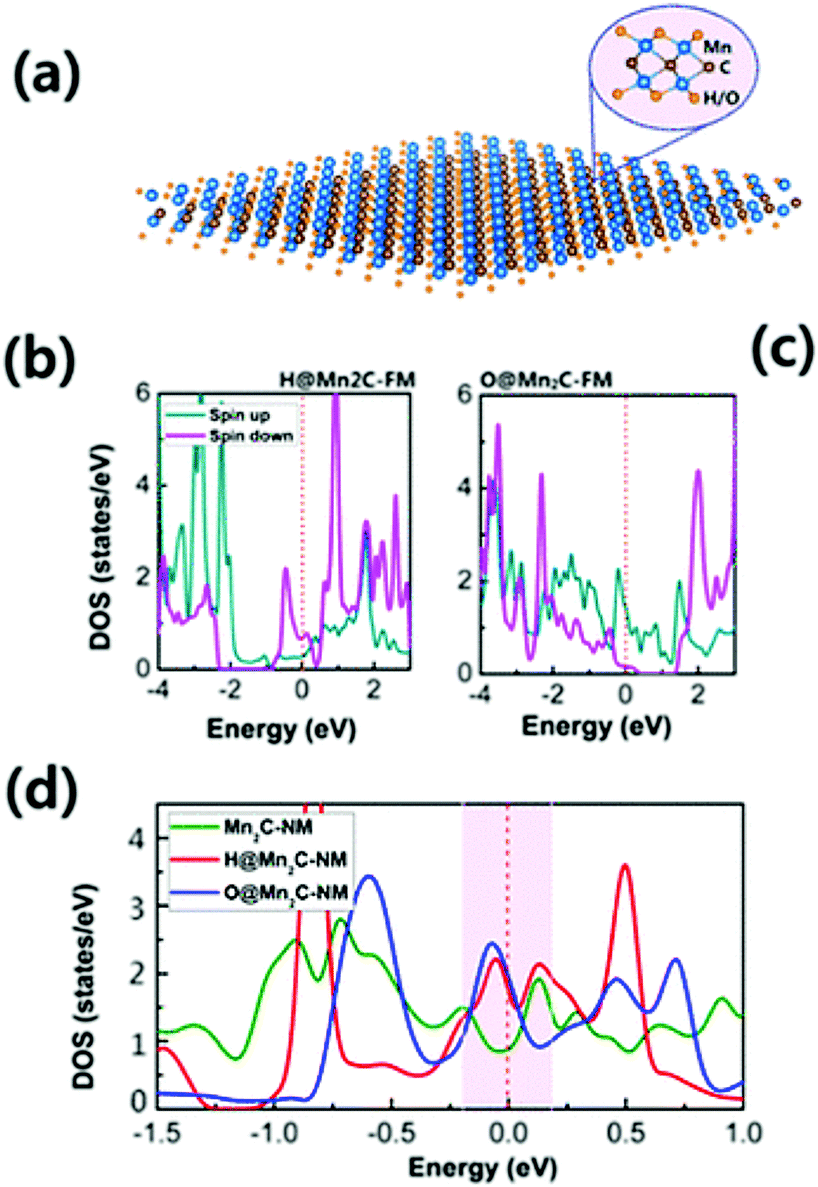 | ||
| Fig. 4 (a) Structural geometry under complete hydrogenation/oxygenation for the Mn2C monolayer, (b) total density of states for hydrogenated Mn2C, (c) total density of states for the oxygenated Mn2C monolayer and (d) comparison of the total density of states for the NM state of the Mn2C monolayer before and after hydrogenation/oxygenation,134 reproduced by permission of the American Chemical Society. | ||
4.7 Defect tuned magnetism
The creation of defects/vacancies, surface functionalization by organic groups, doping of p-block elements, or intercalation of heavy metals or metal oxides not only induces magnetism in 2D materials,24,54,104,135,136 but also leads to significant changes in their electronic properties. For instance, enhanced ferromagnetism was observed in 2D graphene, and the WS2 and MoS2 TMDs through defect engineering.136–138 Defects are advantageous because they can induce magnetism even in nonmagnetic materials and the formation of trapping sites for gaseous pollutants takes place in the presence of defects.139,140 However, defects adversely affect the structural stability of a system; they can even induce plasticity in a BN sheet.141 When following standard synthesis approaches for layered MXene materials, atomic defect formation is unavoidable.142 It is suggested that the defect formation process in MXenes has quite different results to that in other 2D lightweight materials due to their complex structure. Bandyopadhyay et al. introduced a single vacancy in the Ti2CO2 system. As a result, Ti2CO2 showed a semiconductor to metal transition rather than the semiconducting nature of Ti2CO2, which possesses a bandgap of 0.25 eV. Unlike the metallic nature of Ti2NO2, incorporation of defects (Ti or O) resulted in semiconducting behavior.140 Zhang et al. synthesized monolayer Ti3C2Tx MXene (named MX-as) by a LiF/HCl etching method. The MXene was then annealed in a H2 atmosphere and denoted by MX-100, MX-300, and MX-500 where the number refers to the annealing temperature.84 Ti3C2Tx showed very weak paramagnetism while H2 annealing improved the saturation magnetization although ferromagnetism was observed after annealing at 500 °C as shown in Fig. 5a–d. The magnetic susceptibility (χ) versus temperature plots at one kOe applied field for MX-as, MX-100, MX-300, and MX-500 are shown in Fig. 5a; all samples exhibit a Curie-type paramagnetism component, and the χ−1(T) curves (inset) of MX-as, MX-100, and MX-300 were fitted well with the Curie law. On the other hand, MX-500 does not follow the Curie law which suggests magnetic ordering within the sample. The fitted straight lines for MX-as, MX-100, and MX-300 almost go through the origin, indicating pure Curie-type paramagnetism. However, at higher temperature (180 to 300 K range), as shown in Fig. 5b, great deviations from the Curie law were observed. Fig. 5c shows the M–H curves for all samples obtained at 2 K and 65 kOe applied field. For MX-as (Ms ∼ 0.025 emu g−1), the saturation magnetization was further enhanced with increasing annealing temperature. At 300 K temperature, the MX-as, MX-100, and MX-300 M–H curves show pure linear diamagnetism, while MX-500 exhibits a non-linear relation between M and H. Fig. 5d depicts the hysteresis loops of MX-500 at 2 and 300 K temperature. The coercive field (Hc ∼ 84 Oe) and remnant magnetization (Mr ∼ 0.002 emu g−1) at 2 K are evidence of ferromagnetism. Theoretical investigations revealed that Ti–C vacancy pairs were generated during the exfoliation process. As the annealing temperature increases, the C vacancies created by annealing form more Ti–C vacancy pairs due to the inhomogeneous and uncontrollable nature of the annealing process. Thus, H2 annealing acts as the major magnetism source that produces different kinds of Ti–C vacancy pairs. During the experimental preparation, some atomic disorder is always present. In this context, Sang and coworkers showed the presence of Ti vacancies in Ti3C2 experimentally through STM analysis.142 The atomic disorder greatly influences the magnetic as well as electric properties. Hu and coworkers investigated an O-vacancy-line (OVL)-defective armchair-edged Ti2CO2 MXene ribbon. It is reported that the pristine Ti2CO2 ribbon is an NM semiconductor, but the presence of the OVL induces significant magnetism. It is proposed that the OVL position plays an important role in the carrier polarity and spin polarity mobility behavior.143 On the other hand, Zhou et al. studied how the magnetic and electric properties of Ti4N3 MXene nanosheets behave in the presence of defects (atomic vacancies, Frenkel-type) and transition metal (Z = Sc, V and Zr) doping through first-principles based calculations. It was observed that both surface Ti and subsurface N atom vacancies are stable and contribute to the magnetism of the Ti4N3 nanosheets. The total magnetic moment decreased for the Frenkel-type defect system because the indirect magnetic exchange was enhanced between the Ti atoms bridged by N atoms. Meanwhile, large magnetism was obtained in the doped systems. It was proposed that direct magnetic exchange between surface Z and Ti atoms induces the larger magnetism in the doped systems.144 Therefore, tailoring of defects makes MXenes promising candidates for various applications.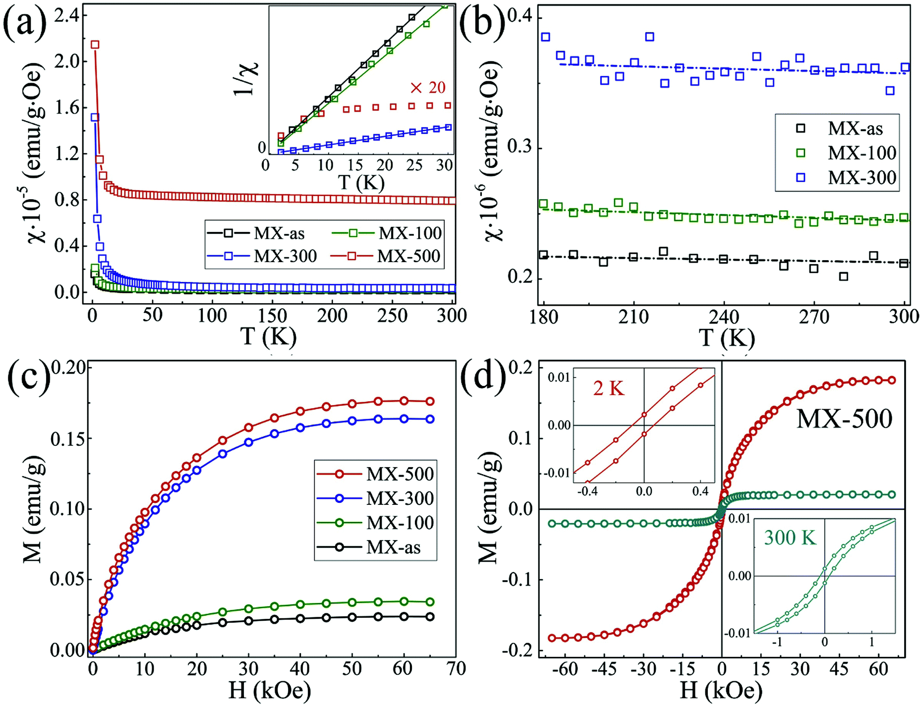 | ||
| Fig. 5 (a) Typical χ(T) curves in the range of 2–300 K at one kOe applied field (inset shows 1/χ–T curves, and the intensity for MX-500 was amplified 20 times to make it more distinct), (b) close-ups of the χ(T) curves of MX-as, MX-100, and MX-300, (c) magnetic moment (M) versus applied field (H) curves at 2 K, (d) hysteresis loops of MX-500 measured at 2 and 300 K,84 reproduced by permission of Elsevier. | ||
5 Applications
Apart from the poor magnetic properties of carbon based nanomaterials, MXenes provide a chance to achieve robust magnetism along with the benefits of half-metallicity that are valuable for spin-based devices. For instance, the Cr2C and Mn2C MXenes are predicted to be intrinsically magnetic. Some of the important uses of MXenes are:5.1 Cancer theranostics
The impressive properties of MXenes, such as high surface to volume ratio, high mechanical stability, ultra thinness, and rich surface chemistry, make them desirable materials for biomedical applications. For instance, 2D MXene flakes and quantum dots have been explored for potential applications in antibacterial materials and multicolor cellular imaging.145,146 MXenes exhibit strong absorption in the near-infrared region (IR), which permits maximum penetration of radiation through the tissues, which demonstrates their applicability in tissue engineering. Meanwhile, the metallic conductivity of MXenes and their high volumetric capacitance support their use in high reliability and low noise bio-sensors. Thanks to their rich chemistry, MXenes possess plenteous reactive sites that decrease the complications of drug functionalization and enzymes. More interestingly, the photothermal conversion capabilities of MXene (Ti3C2) establish it for efficient use in photothermal therapy of tumors. Photothermal therapy (PTT) is a therapeutic strategy that involves destroying tumor cells through hyperthermia. This technique can be considered as an alternative treatment approach to the traditional radiotherapy, surgery, or chemotherapy cancer therapies. These characteristics render Ti3C2 a promising candidate for biomedical applications.145,147 For the first time, Lin et al. demonstrated that ultrathin titanium carbide (Ti3C2) nanosheets have an intrinsic photothermal conversion capability and could be utilized for PTT of tumors.147 However, Ti3C2 exhibits a single photothermal conversion functionality that can be modified by using other functional materials to achieve good performance along with special functionalities. In this direction, Liu et al. prepared magnetic Fe3O4 nanocrystals on the surface of MXenes for cancer theranostics. High T2 relaxivity (394.2 mM−1 s−1) and efficient contrast-enhanced magnetic resonance imaging (MRI) of tumors were observed for the Ti3C2–iron oxide nanoparticle composites.98 Similarly, Zong and coworkers148 achieved high in vivo biocompatibility with GdW10@Ti3C2 composite nanosheets.5.2 Spintronics
Spintronics is the study of the intrinsic spin of the electron along with its fundamental electronic charge. Generally, bare MXenes possess metallic transport character owing to the partially occupied d-shells of the transition metal atoms. Strain, electric field, doping, defects, and functionalization of MXenes result in interesting electrical properties ranging from metal to half-metal, superconductor, semiconductor and topological insulator.149,150 For example, the Ti2C and Ti2N monolayers are predicted to exhibit nearly half-metallic ferromagnetism.128 On the other hand, the double transition metal element based Mo2MC2O2 MXenes (where M refers to Ti, Zr, or Hf) were found to be robust quantum spin Hall insulators.151 Typically, the outer layers of layered MXenes significantly affect the electronic properties of MXenes, in comparison to the inner layers. Also, the presence of the electronegative surface terminating groups alters the electronic properties of MXenes. The d-electrons of the transition metal construct the DOS around the Fermi surface while the p-electrons of the terminating groups such as O and F form the DOS below (−3 to −5 eV range) the Fermi surface.103,152–154 When the p-electrons of the terminating groups interact with the d-electrons of the transition metal, the electronegative terminating groups accept either one or two electrons from the d-subshell of the transition metal. Consequently, a new energy band forms with lower DOS density around the Fermi surface. Therefore, a finite bandgap is achieved by the functionalization of MXenes. It is reported that surface terminating groups (F, OH, O) or other atoms are eventually present during the experimental preparation of MXenes. Most importantly, functionalized MXenes are found to be thermodynamically more compatible than unfunctionalized MXenes. Thus, the presence of terminating groups cannot be neglected, which helps in making a material according to the requirements of the application and realizing the physics behind it.155,156 In this direction, many research groups have studied the effect of these functional groups on the magnetic and electric properties. Si and coworkers104 observed ferromagnetic behavior in a Cr2C crystal. The itinerant Cr d-electrons result from the ferromagnetism and also induce half-metallicity with a gap of 2.85 eV. On the other hand, He et al.109 observed the effect of various surface functional groups on the magnetic and electric properties of Mn2CT2 (T = F, Cl, OH, O, and H) MXenes and predicted that Cl and OH quantitatively influence the magnetic properties and O and H qualitatively influence the magnetic properties. Among them, the M2CF2 MXene showed intrinsic half-metallic nature with a wide energy gap (0.9 eV). Li et al. investigated asymmetric MXene/monolayer transition metal dichalcogenide heterostructures and achieved half-metallicity in many MXene/monolayer transition metal dichalcogenides such as Cr2CO/MoS2, Cr2CO/WSe2, etc.157 Zhang and coworkers obtained intrinsic ferromagnetism in a metallic 2D layered Cr3C2 material, which converted from a metallic ferromagnet to a half-metallic ferromagnet after applying strain. Interestingly, larger strains were found to sustain the half-metallic character of the Cr3C2 MXene.106 It is anticipated that these kinds of ferromagnetic half-metal MXene materials are highly desired for designing next-generation spin based devices such as magnetic sensors, spin injectors, filters and many more.5.3 Electromagnetic interference shielding and microwave absorption
MXenes are prepared by selective etching of the A layer in the presence of some etchant such as –F rich hydrofluoric acid (HF) solution, which leaves abundant defects/vacancies within the MXenes. Many polarization phenomena and strong dielectric relaxation occur due to these defects, which make MXenes excellent microwave absorbing materials. Likewise, the chemically active surfaces in MXenes and the surface terminating groups such as –OH, –F, and –O also make it possible to modify them or to graft electronegative atoms, molecules, etc., to enhance the EMI performance. Moreover, the main advantage of MXenes over other 2D materials is their lamellar microstructure that provides multi-interfaces and increases multiple reflections. Subsequently, their higher specific surface area, tunable electrical conductivity, good thermal conductivity, and excellent film-forming ability make them preferable to 2D graphene. For example, Fe3O4/graphene capsule (GC) composites, prepared by catalytic chemical vapor deposition and hydrothermal methods, showed a minimum RL value of −32 dB at 8.76 GHz at a thickness of 3.5 mm covering an absorption bandwidth range from 5.4 to 17 GHz.158 On the other hand, sandwich-like MXene/Fe3O4 nanocomposites, synthesized by in situ hydrothermal assembly of Fe3O4 nanoparticles on MXene nanosheets demonstrated a minimum RL of −45.1 dB at 3.9 GHz at thickness 3.5 mm with absorption bandwidth in the range of 8.9 to 12.4 GHz.159 MXene/Fe3O4 with a unique morphology showed a better absorption performance than Fe3O4/graphene at a similar thickness. These outstanding properties of 2D MXene composites offer extensive applications in EMI and microwave absorption and other technological applications. Electromagnetic interference (EMI) is a growing worldwide problem. This electromagnetic pollution affects not only electronic devices, radar systems, and wireless communication by degrading the performance and lifetime, but also affects human health by causing anxiety, sleep disorders, etc. Moreover, EM waves can weaken biological immune systems and are even able to break DNA, which endues the genetic code of organisms.160 Therefore, the shielding of electronic devices from the surrounding EM becomes important. It is crucial to understand the shielding mechanism. The primary mechanism is the reflection (SER) of radiation caused by impedance mismatching between the air and the material. Thus, the reflection process requires good electrical conductivity of materials because charge carriers directly interact with the electromagnetic (EM) fields. The second mechanism of EMI shielding is the absorption (SEA) of radiation resulting from EM energy dissipation through Joule heating. Therefore, during absorption electric and/or magnetic dipoles interact with the EM radiation. The third mechanism is the multiple reflections (SEM) that arise due to successive reflections between the internal planes of the material walls. Thus the total EMI shielding is| SET = SER + SEA + SEM | (1) |
It is a well-known fact that MXenes have metallic conductivity and many MXenes possess an intrinsic magnetic moment that may fulfill the requirement of permittivity losses and permeability losses. However, moderated conductivity is required to prevent forefront reflection. It is reported that 2D MXene structures containing more than one element can improve the EMI performance due to the appropriate combination of electric and magnetic materials. Therefore MXenes can be decorated with different high permeability as well as high permittivity materials including magnetic elements (Fe, Ni, Co), conducting polymers (PPy, PANI, PEDOT), lightweight carbon (i.e., graphene, carbon nanotubes, carbon fibers), ceramics, metals (Ag, Cu, etc.)/alloys or metal oxides such as Fe3O4, ZnO and many others. In 2016, two research groups, Han and coworkers, and Shahzad et al., reported EMI shielding studies on MXenes that established 2D MXenes as versatile materials for EMI shielding applications.162,163 Feng et al. studied the Ni-modified Ti3C2 MXene in the frequency range of 2–18 GHz.164 The effective absorption bandwidth is greatly broadened, especially at lower frequencies of 2–8 GHz. They predict that the synergistic effect of dielectric loss and magnetic loss and the structure is responsible for broadening the effective microwave absorption bandwidth. Wang et al. synthesized a sandwich-like MoS2/TiO2/Ti3C2Tx structure by a hydrothermal method.165 At 2.5 mm thickness of the MoS2/TiO2/Ti3C2Tx absorber, the absorption bandwidth was found to be 2.6 GHz. Shan and coworkers decorated NiFe2O4 with Ti3C2Tx MXene composites via an in situ chemical co-precipitation method.166 A bandwidth of 7.68 GHz was achieved for the NiFe2O4 and Ti3C2Tx composite. Miao et al. achieved excellent flexibility and EMI shielding SET with silver nanowires (AgNWs) intercalated into Ti3C2Tx MXene composite films. Silver and MXenes both have good conductivity. Thus one-dimensional nanocellulose (NC) was used with the films to make less insulating contacts between the two conducting materials.167 The AgNWs in Ti3C2Tx MXene nanosheets demonstrated an absorption-dominant EMI shielding mechanism. It was predicted that the “bricks-and-mortar” layered structure maintains the multiple internal reflections and improves the absorption process. The cellular structure with tiny pores gives rise to many scattering interfaces, and the multiple reflections further increase the total EMI shielding effectiveness. Raagulan and coworkers synthesized an MXene–PAT–poly(p-aminophenol)–polyaniline copolymer composite with good electrical conductivity of 7.813 S cm−1. The MXene–PAT–PANI–PpAP composite showed an EMI shielding effectiveness of 45.18 dB at 8.2 GHz.168 The PAT solution was predicted to be an influential ingredient to disperse the MXene and intercalate the conductive polymers within the MXene to enable the expansion of the more conductive network and different structural features.
Liu et al. prepared 2D TiO2/Ti3C2Tx/Fe3O4 composites by a hydrothermal reaction.187Fig. 6a–d show the real/imaginary permittivities/permeabilities while Fig. 6e–h indicates 3D reflection loss (RL) plot and RL plot for various thickness for TiO2/Ti3C2Tx/Fe3O4 composites. In comparison to bare Fe3O4 nanoparticles, for which the permittivity is almost independent of frequency, the presence of TiO2/Ti3C2Tx results in frequency dependence with improved ε′ and ε′′ values. This improvement results from the integrated polarization produced in the heterogeneous structure along with the presence of amorphous carbon in the MXene. Subsequently, fluctuation of the μ′ value of TiO2/Ti3C2Tx/Fe3O4 appears in the 2–18 GHz range. Apart from this, the μ′′ value shows less difference at 2–7 GHz, but upon adding TiO2/Ti3C2Tx it increases in the 7 to 18 GHz frequency range. A superior RL value of −57.3 dB was achieved at 10.1 GHz and at thickness 1.9 mm with bandwidth (i.e. 2 GHz) below −10 dB as shown in Fig. 6e. The RL values of TiO2/Ti3C2Tx/Fe3O4 can be adjusted by changing the thickness as depicted in Fig. 6f–h. The heterostructure TiO2/Ti3C2Tx/Fe3O4 comprises several interfaces and triple-junctions, and the ultra-small size Fe3O4 also contributes to the multiple interfaces. Consequently, bound charges are trapped at these multi-interfaces and triple-junctions which causes the interfacial polarization and relaxation processes. The benefit of ultra-small Fe3O4 is the ease of constructing a conducting path with the MXene. Thus, easy electron movement between Fe3+, Fe2+ and Ti3C2Tx takes place through these conductive structures.
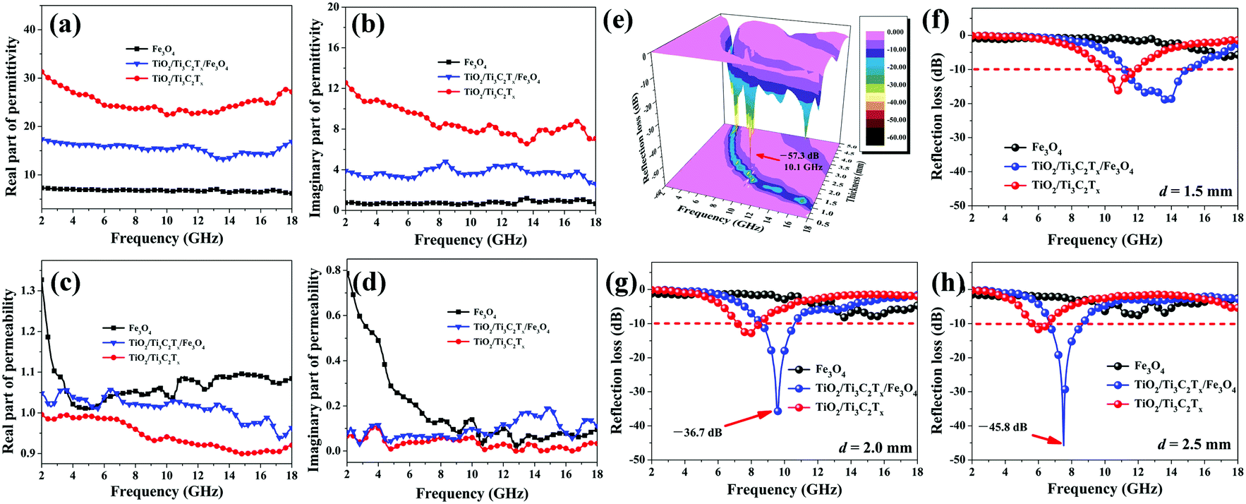 | ||
| Fig. 6 (a) Real and (b) imaginary parts of complex permittivities, (c) real and (d) imaginary parts of complex permeabilities, (e) 3D profile of the RL for the TiO2/Ti3C2Tx/Fe3O4 composite and (f–h) RL values at various thicknesses,187 reproduced by permission of Elsevier. | ||
Similarly, other researchers used the conducting polymer PANI in the Ti3C2/Fe3O4/PANI composite and obtained an optimal RL as low as −40.3 dB and a bandwidth of 5.2 GHz at a thickness of only 1.9 mm.176 The advantage of heterogeneous interfaces with MXenes is the occurrence of significant defect polarization, interfacial polarization, and multiple reflections between these interfaces that improve the EMI and microwave performance. The use of MXene within composites makes the heterostructure versatile because MXene is enable to connect through the hydrogen bonding with other materials. Also MXene accelerates the electron hooping within MXene based heterostructure and thus enhances the EMI shielding and absorption performances. Some of the studied MXene based composites along with their performance are listed in Table 1. It is concluded that the tunable electric and magnetic properties of MXenes favor their wide use as excellent EMI shielding materials. In addition, the hydrophilic nature of MXenes helps in making MXene–polymer based composites, which is beneficial in making polymer based flexible and smart electronic devices. Therefore, MXene based composites have great potential in the field of EMI shielding applications.
| Materials | RLmin/SETa (dB) | Absorption frequency (GHz) | Absorption width/STa frequency range (GHz) | Thickness (mm) | Ref. |
|---|---|---|---|---|---|
| a Values present the EMI shielding efficiencies (SET), all other values in this column represent reflection loss (RL). | |||||
| Annealed Ti3C2Tx | −48.4 | 11.6 | 2.8 | 1.7 | 162 |
| Ti3C2Tx film | 90a | Undetected | 8.4–12.4 | 0.045 | 163 |
| Urchin-like ZnO–Ti3C2Tx | −26.3 | 17.4 | 16.6–18 | 4 | 169 |
| Ti3C2TxNi0.5Zn0.5Fe2O4 | −42.5 | 13.5 | 12–15 | 6.5 | 170 |
| PVB/Ba3Co2Fe24O41/Ti3C2 | −46.3 | 5.8 | 1.6 | 2.8 | 171 |
| Ni-modified Ti3C2 MXene | 22.8 | 11.2 | 6.3 | 1.5 | 164 |
| TiO2/Ti3C2Tx/Fe3O4 | −57.3 | 10.1 | 9.1–11.1 | 1.9 | 172 |
| Ti3C2Tx–Ni nanochain | −49.9 | 11.9 | 10.4–12.5 | 1.75 | 173 |
| CoFe@Ti3C2Tx MXene | −36.29 | 8.56 | 10.32–12.96 | 2.2 | 174 |
| FCI/Ti3C2 | −15.52 | 12.80 | 9.84–18 | 1 | 175 |
| Ti3C2/Fe3O4/PANI | −40.3 | 15.3 | 12.8–18 | 1.9 | 176 |
| Ti3C2Tx/PANI | −56.3 | 13.80 | 8–12.4 | 1.8 | 177 |
| MoS2/TiO2–Ti3C2Tx | 15.8 | 9.9 | 2.6 | 2.5 | 165 |
| NiFe2O4–Ti3C2Tx | −24.7 | 11 | 10.32–18.0 | 1.5 | 166 |
| Co0.2Ni0.4Zn0.4Fe2O4/Ti3C2Tx | −58.4 | 6.2 | 3.8–6.0 | 4.2 | 178 |
| Ti3C2Tx MXene/PVDF | 48.47 ± 3.5a | Undetected | 8.2–12.5 | 2 | 179 |
| MXene–GO | 50.2a | Undetected | 8.2–12.5 | 0.007 | 180 |
| PDMS/MXene/filter paper | 43a | Undetected | 8.2–18 | 0.2 | 181 |
| MXene/RGO hybrid foam | 50.7a | Undetected | 8.2–12.4 | 1.5 | 182 |
| Ti3C2/Ni | −24.3 | 9.8 | 8.66–11.26 | 2.2 | 183 |
| PVA/MXene | 44.4a | Undetected | 8.2–12.4 | 0.027 | 184 |
| Fe3O4@Ti3C2Tx/GF/PDMS | 80a | Undetected | 8.2–12.4 | 1 | 185 |
| Ag/Ti3C2Tx MXene | 42.7a | Undetected | 8.2–12.4 | 0.0169 | 167 |
| MXene aerogel/WPC | 71.3a | Undetected | 8.2–12.4 | 5 | 186 |
6 Conclusions and future possibilities
With the increasing demand for energy storage devices, 2D materials, e.g., 2D graphene, have always been a subject of interest to researchers due to their high surface area, light weight and intriguing physical properties. Pristine graphene is a semimetal, and the lack of d-electrons makes it nonmagnetic. MXenes (with partially filled d-orbitals) show excellent electric and magnetic properties. Interestingly, the chemically synthesized MXenes have abundant functional groups that play a crucial role in modulating the electric and magnetic properties of MXenes. Thus, desirable properties can be obtained in MXene based composites according to the demands of the potential application. This review paper is mainly focused on electrical and magnetic property based applications such as cancer theranostics, electromagnetic interference shielding, and spintronics. MXenes have a high melting point, high surface area, hydrophilic nature, superior electrical conductivity, brittleness, thermal conductivity, compositional variability, etc., and these properties make them highly desirable for potential applications. However, MXenes are not fully explored yet. The etching method is widely used to prepare MXenes using HF or HCl and fluoride salt mixture based etchants. The acid-based solution is tough to handle and also releases harmful gases. This is an excellent opportunity for scientists to develop cost-effective and eco-friendly methods for synthesizing MXenes. The electric and magnetic properties of many MXenes have not been explored experimentally. The study of such MXenes may be useful in the fabrication of spin-based devices. The multiple interfaces and junctions (occurring in ternary and quaternary composites) improve the EMI shielding performance. MXene based ternary and quaternary composites containing intrinsic and/or extrinsic polymers, lightweight carbon allotropes, and dielectric materials need to be discovered. Furthermore, lamellar MXenes have the advantage of large interlayer spacing between their layers. A study of large size cation intercalation between MXene layers may be helpful in searching for potential materials for energy storage devices. Even though MXenes have shown applicability in biomedical applications such as PTT, the bio-compatibility of MXenes still needs to be explored.Conflicts of interest
There are no conflicts to declare.Acknowledgements
V. Shukla acknowledges the Indian Institute of Technology Kharagpur and MHRD, India for providing financial assistance to carry out the research work. V. Shukla wishes to thank Dr S. K. Srivastava for providing a conducive environment to write this manuscript.References
- K. S. Novoselov, A. K. Geim, S. V. Morozov, D. Jiang, Y. Zhang, S. V. Dubonos, I. V. Grigorieva and A. A. Firsov, Science, 2004, 306, 666–669 CrossRef CAS.
- J. C. Meyer, A. K. Geim, M. I. Katsnelson, K. S. Novoselov, T. J. Booth and S. Roth, Nature, 2007, 446, 60–63 CrossRef CAS.
- J. Zhao, H. Liu, Z. Yu, R. Quhe, S. Zhou, Y. Wang, C. C. Liu, H. Zhong, N. Han and J. Lu, et al. , Prog. Mater. Sci., 2016, 83, 24–151 CrossRef CAS.
- A. Molle, C. Grazianetti, L. Tao, D. Taneja, M. H. Alam and D. Akinwande, Chem. Soc. Rev., 2018, 47, 6370–6387 RSC.
- B. J. Ryan, M. P. Hanrahan, Y. Wang, U. Ramesh, C. K. Nyamekye, R. D. Nelson, Z. Liu, C. Huang, B. Whitehead and J. Wang, et al. , Chem. Mater., 2020, 32, 795–804 CrossRef CAS.
- H. Oughaddou, H. Enriquez, M. R. Tchalala, H. Yildirim, A. J. Mayne, A. Bendounan, G. Dujardin, M. A. Ali and A. Kara, Prog. Surf. Sci., 2015, 90, 46–83 CrossRef CAS.
- W.-J. Zhang and K.-J. Huang, Inorg. Chem. Front., 2017, 4, 1602–1620 RSC.
- S. Santhosh and A. A. Madhavan, Advances in Science and Engineering Technology International Conferences (ASET), 2019, pp. 1–5 Search PubMed.
- A. Carvalho, M. Wang, X. Zhu, A. S. Rodin, H. Su and A. H. C. Neto, Nat. Rev. Mater., 2016, 1, 1–16 CrossRef.
- A. Khandelwal, K. Mani, M. H. Karigerasi and I. Lahiri, Mater. Sci. Eng., B, 2017, 221, 17–34 CrossRef CAS.
- M. Akhtar, G. Anderson, R. Zhao, A. Alruqi, J. E. Mroczkowska, G. Sumanasekera and J. B. Jasinski, npj 2D Mater. Appl., 2017, 1, 1–13 CrossRef.
- K. Wang, L. Li, T. Zhang and Z. Liu, Energy, 2014, 70, 612–617 CrossRef CAS.
- A. Pal, M. P. Sk and A. Chattopadhyay, Mater. Adv., 2020, 1, 525–553 RSC.
- W. Liu, J.-j. He, Z.-g. Li, W.-l. Jiang, J.-b. Pang, Y. Zhang and Y. Sun, Phys. Scr., 2012, 85, 055806 CrossRef.
- Y. Zhou, Y. Huang, J. Pang and K. Wang, J. Power Sources, 2019, 440, 227149 CrossRef CAS.
- X. Zhan, C. Si, J. Zhou and Z. Sun, Nanoscale Horiz., 2020, 5, 235–258 RSC.
- L. He, C. Tan, C. Sheng, Y. Chen, F. Yu and Y. Chen, Dalton Trans., 2020, 49, 9268–9273 RSC.
- X. Zhu, X. Huang, R. Zhao, K. Liao and V. Chan, Sustainable Energy Fuels, 2020, 4, 3566–3573 RSC.
- S. T. Oyama, J. C. Schlatter, J. E. Metcalfe III and J. M. Lambert Jr, Ind. Eng. Chem. Res., 1988, 27, 1639–1648 CrossRef CAS.
- J. N. Coleman, M. Lotya, A. O'Neill, S. D. Bergin, P. J. King, U. Khan, K. Young, A. Gaucher, S. De and R. J. Smith, et al. , Science, 2011, 331, 568–571 CrossRef CAS.
- L. Verger, C. Xu, V. Natu, H.-M. Cheng, W. Ren and M. W. Barsoum, Curr. Opin. Solid State Mater. Sci., 2019, 23, 149–163 CrossRef CAS.
- B. Anasori, M. R. Lukatskaya and Y. Gogotsi, Nat. Rev. Mater., 2017, 2, 1–17 Search PubMed.
- Z. Liu, E. Wu, J. Wang, Y. Qian, H. Xiang, X. Li, Q. Jin, G. Sun, X. Chen and J. Wang, et al. , Acta Mater., 2014, 73, 186–193 CrossRef CAS.
- Q. Gao and H. Zhang, Nanoscale, 2020, 12, 5995–6001 RSC.
- H. Tang, Q. Hu, M. Zheng, Y. Chi, X. Qin, H. Pang and Q. Xu, Prog. Nat. Sci.: Mater. Int., 2018, 28, 133–147 CrossRef CAS.
- Ü. Ö. Akkus, E. Balc and S. Berber, Superlattices Microstruct., 2020, 140, 106433 CrossRef.
- L. Ding, Y. Wei, Y. Wang, H. Chen, J. Caro and H. Wang, Angew. Chem., 2017, 129, 1851–1855 CrossRef.
- X. Xie, S. Chen, W. Ding, Y. Nie and Z. Wei, Chem. Commun., 2013, 49, 10112–10114 RSC.
- H. Liu, C. Duan, C. Yang, W. Shen, F. Wang and Z. Zhu, Sens. Actuators, B, 2015, 218, 60–66 CrossRef CAS.
- W. Y. Chen, X. Jiang, S.-N. Lai, D. Peroulis and L. Stanciu, Nat. Commun., 2020, 11, 1–10 Search PubMed.
- V.-H. Nguyen, B.-S. Nguyen, C. Hu, C. C. Nguyen, D. L. T. Nguyen, M. T. Nguyen Dinh, D.-V. N. Vo, Q. T. Trinh, M. Shokouhimehr and A. Hasani, et al. , Nanomaterials, 2020, 10, 602 CrossRef CAS.
- C. Hao, Y. Liao, Y. Wu, Y. An, J. Lin, Z. Gu, M. Jiang, S. Hu and X. Wang, J. Phys. Chem. Solids, 2020, 136, 109141 CrossRef CAS.
- J. Low, L. Zhang, T. Tong, B. Shen and J. Yu, J. Catal., 2018, 361, 255–266 CrossRef CAS.
- L. Cheng, X. Li, H. Zhang and Q. Xiang, J. Phys. Chem. Lett., 2019, 10, 3488–3494 CrossRef CAS.
- Z. Guo, J. Zhou, L. Zhu and Z. Sun, J. Mater. Chem. A, 2016, 4, 11446–11452 RSC.
- Y. Dong, S. S. K. Mallineni, K. Maleski, H. Behlow, V. N. Mochalin, A. M. Rao, Y. Gogotsi and R. Podila, Nano Energy, 2018, 44, 103–110 CrossRef CAS.
- W. Bao, X. Tang, X. Guo, S. Choi, C. Wang, Y. Gogotsi and G. Wang, Joule, 2018, 2, 778–787 CrossRef CAS.
- H. Lin, Y. Chen and J. Shi, Adv. Sci., 2018, 5, 1800518 CrossRef.
- G. Lv, J. Wang, Z. Shi and L. Fan, Mater. Lett., 2018, 219, 45–50 CrossRef CAS.
- Y. Xie, Y. Dall’Agnese, M. Naguib, Y. Gogotsi, M. W. Barsoum, H. L. Zhuang and P. R. Kent, ACS Nano, 2014, 8, 9606–9615 CrossRef CAS.
- Z. Huang, X. Cui, S. Li, J. Wei, P. Li, Y. Wang and C.-S. Lee, Nanophotonics, 2020, 9(8), 2233–2249 CAS.
- J. Yi, J. Li, S. Huang, L. Hu, L. Miao, C. Zhao, S. Wen, V. N. Mochalin and A. M. Rao, InfoMat, 2020, 2, 601–609 CrossRef CAS.
- P. Sandineni, P. Madria, K. Ghosh and A. Choudhury, Mater. Adv., 2020, 1, 698–707 RSC.
- Y. Cao, X. Zhu, X. Tong, J. Zhou, J. Ni, J. Zhang and J. Pang, Front. Chem. Sci. Eng., 2020, 1–9 Search PubMed.
- Q. Cheng, J. Pang, D. Sun, J. Wang, S. Zhang, F. Liu, Y. Chen, R. Yang, N. Liang and X. Lu, et al. , InfoMat, 2020, 2, 656–697 CrossRef CAS.
- K. Hantanasirisakul, M. Alhabeb, A. Lipatov, K. Maleski, B. Anasori, P. Salles, C. Ieosakulrat, P. Pakawatpanurut, A. Sinitskii and S. J. May, et al. , Chem. Mater., 2019, 31, 2941–2951 CrossRef CAS.
- H. Kim and H. N. Alshareef, ACS Mater. Lett., 2020, 2, 55–70 CrossRef CAS.
- X. Jiang, A. V. Kuklin, A. Baev, Y. Ge, H. Ågren, H. Zhang and P. N. Prasad, Phys. Rep., 2020, 848, 1–58 CrossRef CAS.
- N. K. Chaudhari, H. Jin, B. Kim, D. San Baek, S. H. Joo and K. Lee, J. Mater. Chem. A, 2017, 5, 24564–24579 RSC.
- P. Kuang, J. Low, B. Cheng, J. Yu and J. Fan, J. Mater. Sci. Technol., 2020, 56, 18–44 CrossRef.
- J. Wang, F. Ma, W. Liang and M. Sun, Mater. Today Phys., 2017, 2, 6–34 CrossRef.
- U. Krishnan, M. Kaur, K. Singh, M. Kumar and A. Kumar, Superlattices Microstruct., 2019, 128, 274–297 CrossRef CAS.
- V. Shukla, Nanoscale Adv., 2019, 1, 1640–1671 RSC.
- V. Shukla, Nanoscale Adv., 2020, 2, 962–990 RSC.
- A. Saboor, S. M. Khalid, R. Jan, A. N. Khan, T. Zia, M. U. Farooq, S. Afridi, M. Sadiq and M. Arif, Materials, 2019, 12, 2690 CrossRef CAS.
- J. Prasad, A. K. Singh, K. K. Haldar, V. Gupta and K. Singh, J. Alloys Compd., 2019, 788, 861–872 CrossRef CAS.
- J. Prasad, A. K. Singh, J. Shah, R. Kotnala and K. Singh, Mater. Res. Express, 2018, 5, 055028 CrossRef.
- Y. Zhou, Z. Peng, Y. Chen, K. Luo, J. Zhang and S. Du, Comput. Mater. Sci., 2019, 168, 137–143 CrossRef CAS.
- H. Weng, A. Ranjbar, Y. Liang, Z. Song, M. Khazaei, S. Yunoki, M. Arai, Y. Kawazoe, Z. Fang and X. Dai, Phys. Rev. B: Condens. Matter Mater. Phys., 2015, 92, 075436 CrossRef.
- Z. U. Din Babar, M. Anwar, M. Mumtaz, M. Iqbal, R.-K. Zheng, D. Akinwande and S. Rizwan, 2019, arXiv, arXiv-1908.
- J. Zheng, R. He, Y. Wan, P. Zhao, P. Guo and Z. Jiang, Phys. Chem. Chem. Phys., 2019, 21, 3318–3326 RSC.
- J. L. Hart, K. Hantanasirisakul, A. C. Lang, B. Anasori, D. Pinto, Y. Pivak, J. T. van Omme, S. J. May, Y. Gogotsi and M. L. Taheri, Nat. Commun., 2019, 10, 1–10 CrossRef CAS.
- R. Han, X. Ma, Y. Xie, D. Teng and S. Zhang, RSC Adv., 2017, 7, 56204–56210 RSC.
- K. Huang, G. Liu, Y. Lou, Z. Dong, J. Shen and W. Jin, Angew. Chem., 2014, 126, 7049–7052 CrossRef.
- S. Wei, Y. Xie, Y. Xing, L. Wang, H. Ye, X. Xiong, S. Wang and K. Han, J. Membr. Sci., 2019, 582, 414–422 CrossRef CAS.
- K. Rasool, R. P. Pandey, P. A. Rasheed, S. Buczek, Y. Gogotsi and K. A. Mahmoud, Mater. Today, 2019, 30, 80–102 CrossRef CAS.
- X. Li and L. Zhi, Chem. Soc. Rev., 2018, 47, 3189–3216 RSC.
- Y. Li, S. Huang, C. Wei, C. Wu and V. N. Mochalin, Nat. Commun., 2019, 10, 1–8 CrossRef.
- H. Huang, J. Cui, G. Liu, R. Bi and L. Zhang, ACS Nano, 2019, 13, 3448–3456 CrossRef CAS.
- M. Han, Y. Mu and J. Yu, Mater. Adv., 2020, 1, 421–429 RSC.
- Y. Cao, X. Zhu, J. Jiang, C. Liu, J. Zhou, J. Ni, J. Zhang and J. Pang, Sol. Energy Mater. Sol. Cells, 2020, 206, 110279 CrossRef CAS.
- Z. Wang, F. He, J. Guo, S. Peng, X. Q. Cheng, Y. Zhang, E. Drioli, A. Figoli, Y. Li and L. Shao, Mater. Adv., 2020, 1, 554–568 RSC.
- Y. Cao, X. Zhu, H. Chen, X. Zhang, J. Zhouc, Z. Hu and J. Pang, Sol. Energy Mater. Sol. Cells, 2019, 200, 109945 CrossRef CAS.
- F. Zhang, Z. Zhang, H. Wang, C. H. Chan, N. Y. Chan, X. X. Chen and J.-Y. Dai, Phys. Rev. Mater., 2017, 1, 034002 CrossRef.
- P. Urbankowski, B. Anasori, K. Hantanasirisakul, L. Yang, L. Zhang, B. Haines, S. J. May, S. J. Billinge and Y. Gogotsi, Nanoscale, 2017, 9, 17722–17730 RSC.
- B. Anasori and Û. G. Gogotsi, 2D metal carbides and nitrides (MXenes), Springer, 2019 Search PubMed.
- M. Naguib, M. Kurtoglu, V. Presser, J. Lu, J. Niu, M. Heon, L. Hultman, Y. Gogotsi and M. W. Barsoum, Adv. Mater., 2011, 23, 4248–4253 CrossRef CAS.
- J. Halim, S. Kota, M. R. Lukatskaya, M. Naguib, M.-Q. Zhao, E. J. Moon, J. Pitock, J. Nanda, S. J. May and Y. Gogotsi, et al. , Adv. Funct. Mater., 2016, 26, 3118–3127 CrossRef CAS.
- O. Mashtalir, M. Naguib, V. N. Mochalin, Y. Dall'Agnese, M. Heon, M. W. Barsoum and Y. Gogotsi, Nat. Commun., 2013, 4, 1–7 Search PubMed.
- M. Malaki, A. Maleki and R. S. Varma, J. Mater. Chem. A, 2019, 7, 10843–10857 RSC.
- J. Zhou, X. Zha, X. Zhou, F. Chen, G. Gao, S. Wang, C. Shen, T. Chen, C. Zhi and P. Eklund, et al. , ACS Nano, 2017, 11, 3841–3850 CrossRef CAS.
- Q. Tao, M. Dahlqvist, J. Lu, S. Kota, R. Meshkian, J. Halim, J. Palisaitis, L. Hultman, M. W. Barsoum and P. O. Persson, et al. , Nat. Commun., 2017, 8, 1–7 CrossRef.
- M. Ghidiu, M. R. Lukatskaya, M.-Q. Zhao, Y. Gogotsi and M. W. Barsoum, Nature, 2014, 516, 78–81 CrossRef CAS.
- K. Zhang, M. Di, L. Fu, Y. Deng, Y. Du and N. Tang, Carbon, 2020, 157, 90–96 CrossRef CAS.
- A. Reina, X. Jia, J. Ho, D. Nezich, H. Son, V. Bulovic, M. S. Dresselhaus and J. Kong, Nano Lett., 2009, 9, 30–35 CrossRef CAS.
- Y. M. Manawi, A. Samara, T. Al-Ansari and M. A. Atieh, et al. , Materials, 2018, 11, 822 CrossRef.
- C. Xu, L. Wang, Z. Liu, L. Chen, J. Guo, N. Kang, X.-L. Ma, H.-M. Cheng and W. Ren, Nat. Mater., 2015, 14, 1135–1141 CrossRef CAS.
- D. Geng, X. Zhao, Z. Chen, W. Sun, W. Fu, J. Chen, W. Liu, W. Zhou and K. P. Loh, Adv. Mater., 2017, 29, 1700072 CrossRef.
- S. Chaitoglou, T. Giannakopoulou, T. Speliotis, A. Vavouliotis, C. Trapalis and A. Dimoulas, Nanotechnology, 2019, 30, 125401 CrossRef CAS.
- W. Sun, X. Wang, J. Feng, T. Li, Y. Huan, J. Qiao, L. He and D. Ma, Nanotechnology, 2019, 30, 385601 CrossRef CAS.
- A. Kumar and D. Nanda, Superhydrophobic Polymer Coatings, Elsevier, 2019, pp. 43–75 Search PubMed.
- X. Li, W. Cai, J. An, S. Kim, J. Nah, D. Yang, R. Piner, A. Velamakanni, I. Jung and E. Tutuc, et al. , Science, 2009, 324, 1312–1314 CrossRef CAS.
- N. D. Mermin and H. Wagner, Phys. Rev. Lett., 1966, 17, 1133 CrossRef CAS.
- I. A. Calafell, J. Cox, M. Radonjić, J. Saavedra, F. G. de Abajo, L. Rozema and P. Walther, npj Quantum Inf., 2019, 5, 1–7 CrossRef.
- P. Huang, P. Zhang, S. Xu, H. Wang, X. Zhang and H. Zhang, Nanoscale, 2020, 12, 2309–2327 RSC.
- K.-L. Chiu, 2018, arXiv preprint arXiv:1804.02870.
- G. Song, M. Ranjbar and R. A. Kiehl, Commun. Phys., 2019, 2, 1–8 CAS.
- Z. Liu, M. Zhao, H. Lin, C. Dai, C. Ren, S. Zhang, W. Peng and Y. Chen, J. Mater. Chem. B, 2018, 6, 3541–3548 RSC.
- S. Mathew, K. Gopinadhan, T. Chan, X. Yu, D. Zhan, L. Cao, A. Rusydi, M. Breese, S. Dhar and Z. Shen, et al. , Appl. Phys. Lett., 2012, 101, 102103 CrossRef.
- J.-H. Chen, L. Li, W. G. Cullen, E. D. Williams and M. S. Fuhrer, Nat. Phys., 2011, 7, 535–538 Search PubMed.
- R. Nair, M. Sepioni, I.-L. Tsai, O. Lehtinen, J. Keinonen, A. Krasheninnikov, T. Thomson, A. Geim and I. Grigorieva, Nat. Phys., 2012, 8, 199–202 Search PubMed.
- G. Khurana, N. Kumar, R. Kotnala, T. Nautiyal and R. Katiyar, Nanoscale, 2013, 5, 3346–3351 RSC.
- M. Khazaei, M. Arai, T. Sasaki, C.-Y. Chung, N. S. Venkataramanan, M. Estili, Y. Sakka and Y. Kawazoe, Adv. Funct. Mater., 2013, 23, 2185–2192 CrossRef CAS.
- C. Si, J. Zhou and Z. Sun, ACS Appl. Mater. Interfaces, 2015, 7, 17510–17515 CrossRef CAS.
- Z. Zhang, X. Liu, J. Yu, Y. Hang, Y. Li, Y. Guo, Y. Xu, X. Sun, J. Zhou and W. Guo, Wiley Interdiscip. Rev.: Comput. Mol. Sci., 2016, 6, 324–350 CAS.
- Y. Zhang and F. Li, J. Magn. Magn. Mater., 2017, 433, 222–226 CrossRef CAS.
- H. Kumar, N. C. Frey, L. Dong, B. Anasori, Y. Gogotsi and V. B. Shenoy, ACS Nano, 2017, 11, 7648–7655 CrossRef CAS.
- Y. Zhong, X. Xia, F. Shi, J. Zhan, J. Tu and H. J. Fan, Adv. Sci., 2016, 3, 1500286 CrossRef.
- J. He, P. Lyu and P. Nachtigall, J. Mater. Chem. C, 2016, 4, 11143–11149 RSC.
- L. Hu, X. Wu and J. Yang, Nanoscale, 2016, 8, 12939–12945 RSC.
- M. Chhowalla, H. S. Shin, G. Eda, L.-J. Li, K. P. Loh and H. Zhang, Nat. Chem., 2013, 5, 263–275 CrossRef.
- J. B. Goodenough, Scholarpedia, 2008, 3, 7382 CrossRef.
- A. Ono and S. Ishihara, Phys. Rev. Lett., 2017, 119, 207202 CrossRef.
- N. C. Frey, H. Kumar, B. Anasori, Y. Gogotsi and V. B. Shenoy, ACS Nano, 2018, 12, 6319–6325 CrossRef CAS.
- Y. Yoon, T. A. Le, A. P. Tiwari, I. Kim, M. W. Barsoum and H. Lee, Nanoscale, 2018, 10, 22429–22438 RSC.
- Z. U. D. Babar, J. Fatheema, N. Arif, M. Anwar, S. Gul, M. Iqbal and S. Rizwan, RSC Adv., 2020, 10, 25669–25678 RSC.
- N. C. Frey, A. Bandyopadhyay, H. Kumar, B. Anasori, Y. Gogotsi and V. B. Shenoy, ACS Nano, 2019, 13, 2831–2839 CrossRef CAS.
- Q. Tang, Z. Zhou and P. Shen, J. Am. Chem. Soc., 2012, 134, 16909–16916 CrossRef CAS.
- H. Wang, Y. Wu, J. Zhang, G. Li, H. Huang, X. Zhang and Q. Jiang, Mater. Lett., 2015, 160, 537–540 CrossRef CAS.
- S. Li, J. He, P. Nachtigall, L. Grajciar and F. Brivio, Phys. Chem. Chem. Phys., 2019, 21, 25802–25808 RSC.
- S.-s. Li, S.-j. Hu, W.-x. Ji, P. Li, K. Zhang, C.-w. Zhang and S.-s. Yan, Appl. Phys. Lett., 2017, 111, 202405 CrossRef.
- Y. Hu, X.-Y. Liu, Z.-H. Shen, Z.-F. Luo, Z.-G. Chen and X. Fan, Nanoscale, 2020, 12, 11627–11637 RSC.
- X. Bai, X.-H. Zha, Y. Qiao, N. Qiu, Y. Zhang, K. Luo, J. He, Q. Li, Q. Huang and J. S. Francisco, et al. , Nanoscale, 2020, 12, 3795–3802 RSC.
- G. Wang and Y. Liao, Appl. Surf. Sci., 2017, 426, 804–811 CrossRef CAS.
- Q. Sun, Z. Fu and Z. Yang, J. Magn. Magn. Mater., 2020, 167141 CrossRef CAS.
- Y. Lee, S. B. Cho and Y.-C. Chung, ACS Appl. Mater. Interfaces, 2014, 6, 14724–14728 CrossRef CAS.
- P. Lv, Y.-L. Li and J.-F. Wang, Phys. Chem. Chem. Phys., 2020, 22, 11266–11272 RSC.
- G. Gao, G. Ding, J. Li, K. Yao, M. Wu and M. Qian, Nanoscale, 2016, 8, 8986–8994 RSC.
- J. Yang, X. Zhou, X. Luo, S. Zhang and L. Chen, Appl. Phys. Lett., 2016, 109, 203109 CrossRef.
- A. Bafekry, B. Akgenc, M. Ghergherehchi and F. Peeters, J. Phys.: Condens. Matter, 2020, 32, 355504 CrossRef CAS.
- S. Zhao, W. Kang and J. Xue, Appl. Phys. Lett., 2014, 104, 133106 CrossRef.
- B. Akgenc, A. Mogulkoc and E. Durgun, J. Appl. Phys., 2020, 127, 084302 CrossRef CAS.
- Y. Zhang, X.-H. Zha, K. Luo, N. Qiu, Y. Zhou, J. He, Z. Chai, Z. Huang, Q. Huang and Y. Liang, et al. , J. Phys. Chem. C, 2019, 123, 6802–6811 CrossRef CAS.
- X. Zhang, T. He, W. Meng, L. Jin, Y. Li, X. Dai and G. Liu, J. Phys. Chem. C, 2019, 123, 16388–16392 CrossRef CAS.
- J. Sun, J. Qian, W. Wang, P. Wang, Y. Xu, L. Liao and S. Ye, J. Supercond. Novel Magn., 2018, 31, 1241–1245 CrossRef CAS.
- X. Ding, T. Liu, S. Ahmed, N. Bao, J. Ding and J. Yi, J. Alloys Compd., 2019, 772, 740–744 CrossRef CAS.
- C.-S. Park, Y. Zhao, H. Kim, Y. Shon and E. K. Kim, Chem. Commun., 2014, 50, 12930–12932 RSC.
- S. Ahmed, P. Viboon, X. Ding, N. Bao, Y. Du, T. Herng, J. Ding and J. Yi, J. Alloys Compd., 2018, 746, 399–404 CrossRef CAS.
- D. Ghosh and S. K. Pati, Phys. Chem. Chem. Phys., 2017, 19, 636–643 RSC.
- A. Bandyopadhyay, D. Ghosh and S. K. Pati, Phys. Chem. Chem. Phys., 2018, 20, 4012–4019 RSC.
- O. Cretu, Y.-C. Lin and K. Suenaga, Nano Lett., 2014, 14, 1064–1068 CrossRef CAS.
- X. Sang, Y. Xie, M.-W. Lin, M. Alhabeb, K. L. Van Aken, Y. Gogotsi, P. R. Kent, K. Xiao and R. R. Unocic, ACS Nano, 2016, 10, 9193–9200 CrossRef CAS.
- T. Zhou, W. Zhao, K. Yang, Q. Yao, Y. Li, B. Wu and J. Liu, Appl. Sci., 2020, 10, 2450 CrossRef CAS.
- R. Hu, Y. Li, Z. Zhang, Z. Fan and L. Sun, J. Mater. Chem. C, 2019, 7, 7745–7759 RSC.
- J. Xuan, Z. Wang, Y. Chen, D. Liang, L. Cheng, X. Yang, Z. Liu, R. Ma, T. Sasaki and F. Geng, Angew. Chem., Int. Ed., 2016, 55, 14569–14574 CrossRef CAS.
- Q. Xue, H. Zhang, M. Zhu, Z. Pei, H. Li, Z. Wang, Y. Huang, Y. Huang, Q. Deng and J. Zhou, et al. , Adv. Mater., 2017, 29, 1604847 CrossRef.
- H. Lin, X. Wang, L. Yu, Y. Chen and J. Shi, Nano Lett., 2017, 17, 384–391 CrossRef CAS.
- L. Zong, H. Wu, H. Lin and Y. Chen, Nano Res., 2018, 11, 4149–4168 CrossRef CAS.
- J. Lei, A. Kutana and B. I. Yakobson, J. Mater. Chem. C, 2017, 5, 3438–3444 RSC.
- Y. Liang, M. Khazaei, A. Ranjbar, M. Arai, S. Yunoki, Y. Kawazoe, H. Weng and Z. Fang, Phys. Rev. B, 2017, 96, 195414 CrossRef.
- C. Si, K.-H. Jin, J. Zhou, Z. Sun and F. Liu, Nano Lett., 2016, 16, 6584–6591 CrossRef CAS.
- A. Enyashin and A. Ivanovskii, J. Solid State Chem., 2013, 207, 42–48 CrossRef CAS.
- B. Anasori, Y. Xie, M. Beidaghi, J. Lu, B. C. Hosler, L. Hultman, P. R. Kent, Y. Gogotsi and M. W. Barsoum, ACS Nano, 2015, 9, 9507–9516 CrossRef CAS.
- L. Dong, H. Kumar, B. Anasori, Y. Gogotsi and V. B. Shenoy, J. Phys. Chem. Lett., 2017, 8, 422–428 CrossRef CAS.
- Y. Lee, Y. Hwang, S. B. Cho and Y.-C. Chung, Phys. Chem. Chem. Phys., 2014, 16, 26273–26278 RSC.
- L. Li, J. Phys. Chem. C, 2016, 120, 24857–24865 CrossRef CAS.
- B. Li, H. Guo, Y. Wang, W. Zhang, Q. Zhang, L. Chen, X. Fan, W. Zhang, Y. Li and W.-M. Lau, npj Comput. Mater., 2019, 5, 1–8 CrossRef CAS.
- X. Jian, B. Wu, Y. Wei, S. X. Dou, X. Wang, W. He and N. Mahmood, ACS Appl. Mater. Interfaces, 2016, 8, 6101–6109 CrossRef CAS.
- G. Zhao, H. Lv, Y. Zhou, X. Zheng, C. Wu and C. Xu, ACS Appl. Mater. Interfaces, 2018, 10, 42925–42932 CrossRef CAS.
- J. Deng, Q. Wang, Y. Zhou, B. Zhao and R. Zhang, RSC Adv., 2017, 7, 9294–9302 RSC.
- M. C. Ribadeneyra, J. P. de Diego and M. G. González, PhD thesis, Universidad Carlos III de Madrid, 2014, http://hdl.handle.net.
- M. Han, X. Yin, H. Wu, Z. Hou, C. Song, X. Li, L. Zhang and L. Cheng, ACS Appl. Mater. Interfaces, 2016, 8, 21011–21019 CrossRef CAS.
- F. Shahzad, M. Alhabeb, C. B. Hatter, B. Anasori, S. M. Hong, C. M. Koo and Y. Gogotsi, Science, 2016, 353, 1137–1140 CrossRef CAS.
- W. Feng, H. Luo, S. Zeng, C. Chen, L. Deng, Y. Tan, X. Zhou, S. Peng and H. Zhang, Mater. Chem. Front., 2018, 2, 2320–2326 RSC.
- H. Wang and H. Ma, J. Mater. Sci.: Mater. Electron., 2019, 30, 15250–15256 CrossRef CAS.
- D. Shan, J. He, L. Deng, S. Yan, H. Luo, S. Huang and Y. Xu, Results Phys., 2019, 15, 102750 CrossRef.
- M. Miao, R. Liu, S. Thaiboonrod, L. Shi, S. Cao, J. Zhang, J. Fang and X. Feng, J. Mater. Chem. C, 2020, 8, 3120–3126 RSC.
- K. Raagulan, R. Braveenth, B. M. Kim, K. J. Lim, S. B. Lee, M. Kim and K. Y. Chai, RSC Adv., 2020, 10, 1613–1633 RSC.
- Y. Qian, H. Wei, J. Dong, Y. Du, X. Fang, W. Zheng, Y. Sun and Z. Jiang, Ceram. Int., 2017, 43, 10757–10762 CrossRef CAS.
- Y. Li, X. Zhou, J. Wang, Q. Deng, M. Li, S. Du, Y.-H. Han, J. Lee and Q. Huang, RSC Adv., 2017, 7, 24698–24708 RSC.
- H. Yang, J. Dai, X. Liu, Y. Lin, J. Wang, L. Wang and F. Wang, Mater. Chem. Phys., 2017, 200, 179–186 CrossRef CAS.
- P. Liu, Z. Yao, V. M. H. Ng, J. Zhou, L. B. Kong and K. Yue, Composites, Part A, 2018, 115, 371–382 CrossRef CAS.
- L. Liang, G. Han, Y. Li, B. Zhao, B. Zhou, Y. Feng, J. Ma, Y. Wang, R. Zhang and C. Liu, ACS Appl. Mater. Interfaces, 2019, 11, 25399–25409 CrossRef CAS.
- C. Zhou, X. Wang, H. Luo, L. Deng, S. Wang, S. Wei, Y. Zheng, Q. Jia and J. Liu, Appl. Surf. Sci., 2019, 494, 540–550 CrossRef CAS.
- S. Yan, C. Cao, J. He, L. He and Z. Qu, J. Mater. Sci.: Mater. Electron., 2019, 30, 6537–6543 CrossRef CAS.
- Y. Wang, X. Gao, L. Zhang, X. Wu, Q. Wang, C. Luo and G. Wu, Appl. Surf. Sci., 2019, 480, 830–838 CrossRef CAS.
- H. Wei, J. Dong, X. Fang, W. Zheng, Y. Sun, Y. Qian, Z. Jiang and Y. Huang, Compos. Sci. Technol., 2019, 169, 52–59 CrossRef CAS.
- P. Liu, Z. Yao, V. M. H. Ng, J. Zhou and L. B. Kong, Mater. Lett., 2019, 248, 214–217 CrossRef CAS.
- K. Rajavel, S. Luo, Y. Wan, X. Yu, Y. Hu, P. Zhu, R. Sun and C. Wong, Composites, Part A, 2020, 129, 105693 CrossRef CAS.
- J. Liu, Z. Liu, H.-B. Zhang, W. Chen, Z. Zhao, Q.-W. Wang and Z.-Z. Yu, Adv. Electron. Mater., 2020, 6, 1901094 CrossRef CAS.
- D. Hu, X. Huang, S. Li and P. Jiang, Compos. Sci. Technol., 2020, 107995 CrossRef CAS.
- Z. Fan, D. Wang, Y. Yuan, Y. Wang, Z. Cheng, Y. Liu and Z. Xie, Chem. Eng. J., 2020, 381, 122696 CrossRef CAS.
- Y. Liu, S. Zhang, X. Su, J. Xu and Y. Li, J. Mater. Sci., 2020, 1–12 Search PubMed.
- X. Jin, J. Wang, L. Dai, X. Liu, L. Li, Y. Yang, Y. Cao, W. Wang, H. Wu and S. Guo, Chem. Eng. J., 2020, 380, 122475 CrossRef CAS.
- V.-T. Nguyen, B. K. Min, Y. Yi, S. J. Kim and C.-G. Choi, Chem. Eng. J., 2020, 124608 CrossRef CAS.
- C. Liang, H. Qiu, P. Song, X. Shi, J. Kong and J. Gu, Sci. Bull., 2020, 65(8), 616–622 CrossRef CAS.
- P. Liu, V. M. H. Ng, Z. Yao, J. Zhou and L. B. Kong, Mater. Lett., 2018, 229, 286–289 CrossRef CAS.
| This journal is © The Royal Society of Chemistry 2020 |