
 Open Access Article
 This Open Access Article is licensed under a
 Creative Commons Attribution 3.0 Unported Licence
Origin of resistive-switching behaviors of chemical solution deposition-derived BiFeO3 thin-film memristors†
Feng
Yang
 *a,
Fen
Liu
b,
Fengqi
Ji
a,
Yanling
Lin
a and
Minghua
Tang
c
*a,
Fen
Liu
b,
Fengqi
Ji
a,
Yanling
Lin
a and
Minghua
Tang
c
aSchool of Materials Science and Engineering, University of Jinan, Jinan 250022, People's Republic of China. E-mail: mse_yangf@ujn.edu.cn
bShandong Provincial Key Laboratory of Preparation and Measurement of Building Materials, University of Jinan, Jinan 250022, People's Republic of China
cHunan Provincial National Defense Key Laboratory of Key Film Materials & Application for Equipments, Xiangtan 411105, People's Republic of China
First published on 8th September 2020
Abstract
Oxide-based memristors have good application prospects in the brain-like computing of the in-memory computing architecture, which can effectively solve the memory wall and power wall problems in the bottleneck of the von Neumann architecture in which computation and storage are physically separated. The ferroelectric-oxide memristor shows more prominent advantages, such as ultra-fast reading and writing speed and extremely low energy consumption. However, the origin of the resistive switching phenomenon of ferroelectric oxides has been controversial. Herein, we used a ferroelectric BiFeO3 memristor as a model system to investigate the ferroresistive and non-ferroresistive-switching behaviors under different applied bias voltages and frequencies. Results showed that the memristive behavior was caused by ferroelectric polarization at high frequencies; conversely, at low frequencies, the memristive behavior originated from the defect electroforming process driven by a large electric field. The ferroelectric-based retention and antifatigue properties of the BiFeO3 memristor were superior to those of electroforming processes based on redox reactions. The mechanism of charge transport through interfacial barriers and the origin of the observed resistive-switching effect were discussed using a metal–insulator–ferroelectric–insulator–semiconductor model. Our findings may explain the controversy over the origin of resistive switches in ferroelectric thin films and pave the way for further ferroelectric-memristor applications.
1. Introduction
A hysteresis loop of current–voltage characteristics can often be observed in a two-terminal device consisting of a sandwich structure, usually a single- or double-layer oxide, sandwiched between two electrodes.1 This behavior, known as resistance switching (RS), is used in memristors or resistive random access memories (RRAM). Oxide-based memristors have good application prospects in the brain-like computing of the in-memory computing architecture,2,3 which can effectively solve the memory wall and power wall problems in the bottleneck of the von Neumann architecture in which computation and storage are physically separated.4 In the past two decades, RS has received extensive attention and in-depth research.5–7 RS in oxides have been attributed to the modification of electrode/oxide interface caused by local redox reaction, the phase-change effect induced by local Joule heat, or by the electroforming process of conductive filaments formed by the electromigration of charged ions in insulating matrix.5,7 In ferroelectric oxides, RS effect has been observed in ferroelectric thin-film capacitors, ferroelectric diodes, ferroelectric tunnel junctions and ferroelectric domain walls.8–18 Ferroelectric oxide-based memristors have attracted great interest17,18 due to the ultra-fast switching speed of the polarization-dependent electronic transport (depending on the polarization inversion time of about 1–2 ps).19 RS effect in a ferroelectric-oxide device is considered to be due to the adjustment of the Schottky barrier height and barrier width at the ferroelectric/electrode interface by switchable ferroelectric polarization.20–25In literature, RS in ferroelectric oxides was interpreted as the modulation effect of ferroelectric polarization. Although ferroelectric oxide is also a kind of oxide, the mechanism of its RS effect is completely different from other oxides. This is quite incredible. Moreover, the RS behavior of ferroelectric materials does not differ significantly from those of other oxides on current –voltage curves. Many scholars are skeptical of ferroelectricity producing RS because even without ferroelectricity, similar RS behavior can still be produced. Therefore, distinguishing ferroelectric RS from that of a nonferroelectric origin is crucial.20–25
Here, we use the BiFeO3 (BFO) memristor with a Pt/BFO/La0.67Sr0.33MnO3 (LSMO) heterostructure9,10,26–30 as a model system to explore the RS origin in ferroelectric oxides. Most ferroelectric oxides generally have a wide band gap (Eg > 3 eV), and therefore have a very small conduction current. Unlike other ferroelectric oxides, BFO, which has a relatively narrow band gap (Eg ∼ 2.8 eV) is more suitable for resistive devices. In BFO devices, a large switching ratio has been observed.8,29,31 It is also found that RS and polarization inversion occur simultaneously when applied voltage reversal.8–10,29,32–34 Is RS determined by polarization reversal? Is it possible that the RS is caused by non-ferroelectricity factors like in other oxides?5,7
In the present work, RS mechanism of the BFO memristor was comprehensively investigated. Using different applied bias voltage and frequencies, we observed two independent switching phenomena; one attributed to ferroelectric switching and the other to the electroforming behavior caused by redox reaction. At high frequencies, we found that the RS behavior was caused by polarization reversal. By contrast, at low frequencies, we observed that the defect-electroforming behavior was driven by the large electric field. The ferroelectric-based retention and antifatigue properties were superior to those of electroforming processes based on redox reactions. The mechanism of charge transport through barriers and the origin of the observed RS effect were discussed.
2. Results
BFO memristors were prepared on a (001) SrTiO3 (STO) single-crystal substrate. A 10 nm-thick LSMO film and a 100 nm-thick BFO film were grown epitaxially onto the substrates by chemical solution deposition (CSD). The circular Pt electrode with 200 μm in diameter was deposited on the BFO layer through a shadow mask by electron-beam evaporation. Fig. 1(a) shows the X-ray diffraction (XRD) θ − 2θ pattern of the BFO/LSMO/STO heterostructure. Only the (00l) (l = 1, 2) peaks was observed in the XRD θ − 2θ patterns. The position of the peaks indicated an epitaxial growth of the pseudocubic phase with the 00l axis parallel to the growth direction. No secondary phases were observed within the resolution limit of the XRD technology. Given that the bulk a-axis lattice constant of BFO is greater than that of STO, strained growth (compressive strain ε = (aSTO − aBFO)/aSTO = −1.53%) existed, where (aSTO = 3.905 Å; aBFO = 3.965 Å).35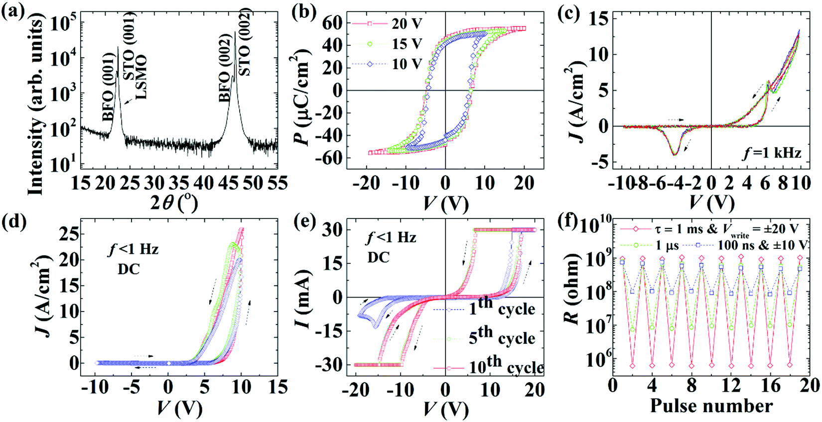 | ||
| Fig. 1 (a) X-ray diffraction pattern of BFO/LSMO/STO heterojunction. (b) The polarization–voltage hysteresis loops of the BFO memristor under different applied voltages. (c and d) Current density–voltage characteristics measured under ±10 V sweep voltage at frequencies of (c) 1 kHz and (d) <1 Hz. (e) Current–voltage behavior measured under ±20 V sweep voltage (1st cycle, 5th, and 10th cycle sweeps). (f) Resistive switching behaviors measured in pulsed-voltage mode for various pulse durations (τ = 1 ms, 1 μs, and 100 ns). Pulsed-voltage stresses ±10 V (20 V) were applied to the devices. Resistance values were evaluated from current values at V = 0.3 V. | ||
The ferroelectricity of BFO memristors at room temperature was examined. Fig. 1(b) shows the ferroelectric hysteresis loops (polarization P vs. voltage V) measured at a frequency of 1 kHz and different applied voltages (10 V, 15 V and 20 V). All P–V loops show saturated rectangularity.36 The very close coercive voltages and remanent polarizations can be observed in the three loops. The coercive voltage of ∼5.6 V guarantees the complete reversal of the ferroelectric polarizations under the applied voltage of 10 V, 15 V and 20 V. The remnant polarization (Pr) of ∼45 μC cm−2 at 15 V was slightly smaller than typical values of [001]-oriented BFO films (∼60 μC cm−2).35,37 The Pr was also smaller than that of our [110]-oriented BFO films (∼70 μC cm−2) prepared by CSD.34 The smaller remnant polarization may be due to the presence of Bi-vacancy defects, which will pin ferroelectric domains. In addition, it may result from the pinning effect of epitaxial strain from STO substrate on ferroelectric domains.
We further examined the hysteresis current density–voltage (J–V) characteristics of BFO devices, whose J–V curves is shown in Fig. 1(c). In this measurement, the voltage was swept as 0 V → +10 V → −10 V → 0 V at f = 1 kHz. Positive and negative current peaks were observed at V = 6.1 V and −4.2 V, respectively. According to the sequence of voltage scanning, the resistance state of the device started from the high resistance state (HRS), changed to low resistance state (LRS) from HRS after the positive current peak, and changed back to HRS from LRS after the negative current peak. As a comparison, we measured the J–V characteristics at DC (f < 1 Hz) and observed no current peak, as shown in Fig. 1(d), which shows the obvious diode rectification characteristics, namely forward conduction and reverse cutoff. In the high-frequency J–V curve of Fig. 1c, a negative differential resistance (NDR),38 which is well known in TiO2-based memristors,39 was also observed in the range from −4.2 V to −5.4 V. In TiO2, the NDR is related to the migration of charged ions.38 However, the two current peaks at 6.1 V and −4.2 V only existed under high frequency, and disappeared for low frequency signal. This was contrary to the law of charged-ion migration. Therefore, our NDR was not caused by the migration of charged ions. The high-frequency peak current were transient currents, such as ferroelectric displacement currents.29 At high frequencies, the peak current corresponded to the transition between high and low resistance states, and the ferroelectric polarization inversion was the predominant of the observed current peaks. Therefore, we can deduced that the polarization reversal at high frequencies was related to the RS in the device.
As shown in Fig. 1(d), under the sweep voltage of ±10 V, a sharp increase in the current at the forward voltage was observed, while at the negative voltage, the current remained very low, similar to the transport characteristics of the diode with forward conduction and reverse cut-off. The sweep sequence is indicated by the arrows. When a bias voltage of ±20 V was applied (Fig. 1(e)), sharp RS was observed at both positive and negative maximum voltages. At the maximum positive voltage, the peak current increased sharply and exceeded 30 mA (i.e., several times larger than low-voltage case). As shown in Fig. 1(e), unlike the case of reverse cut-off under the scanning voltage of ±10 V, the current–voltage (I–V) shape also showed a large current spike when scanning in the direction of −20 V. Careful observation showed that under the action of large voltage, the initial cycle state was not stable, because the first cycle and the fifth cycle did not coincide. The fifth cycle to the tenth cycle basically overlapped. This gradual stabilization strongly suggested that RS was no longer driven by an interface mechanism. RS was likely to be maintained by the electroforming mechanism caused by the movement of defects (vacancies).40 The movement of defects self-aligned into a filamentary network after several scanning cycles, which was consistent with the gradual shift process observed in the experiment. After several RS cycles under high DC voltages of ±20 V, the P–V loop of the BFO memristor measured again, as shown in Fig. S1 (ESI†), indicating that the ferroelectricity is not destroyed by RS. The influence of ferroelectricity on SR becomes a secondary factor and is hidden under the electroforming mechanism.
We investigated the RS characteristics of the device under pulse voltage. Fig. 1(f) shows the pulse duration (τ) and voltage-amplitude dependence of the RS characteristics of BFO devices. We found that for long pulses and large amplitude voltage, the largest resistance in the HRS (RH) and the smallest resistance in the LRS (RL) were obtained. Conversely, under short pulses and small-amplitude voltage, the RH values were smaller and the RL values were larger. Further research showed that RH was less affected by τ, while RL increased as τ decreased. This result indicated that the stability of the LRS was not as good as that of the HRS. It was different from the pure polarization-driven switching mechanism. Therefore, the effects of non-ferroelectricity had always existed. However, fortunately, as the τ decreases, the influence of non-ferroelectric factors decreased. Under a write pulse with an amplitude of ±10 V and τ = 100 ns, a clear RS behavior was observed with RH/RL ≈ 8 (Fig. 1f). When the amplitude was ± 20 V and τ = 1 ms, the larger RH/RL was more than 103. The electroforming effect based on ion migration can produce a larger switching ratio than that driven entirely by ferroelectricity.
We subsequently evaluated the potential of our RS devices for nonvolatile memory applications by performing data-retention and endurance tests. Fig. 2 exhibits the room-temperature retention characteristics of data written with pulses of different amplitudes and pulse widths. LRS or HRS was set by applying positive or negative voltage pulses with different amplitude and width, respectively. The retention data was recorded after applying 103 cycles of voltage stresses at room temperature. Fig. 2(a and b) shows the retention-data after applying a pulse of (±10 V, 100 ns). Both RH and RL slightly decreased with time, but the RH/RL ratio of the device remained approximately 8 for 105 s. The excellent retention performance of the device was similar to that of the ferroelectric polarization of BFO. Fig. 2(c and d) exhibit the results of data retention of the BFO device after applying a pulse of (±20 V, 1 ms). RH decreased with time, whereas RL slightly increased with time. But within 105 s, the RH/RL ratio of the device seriously fluctuated and decreased by nearly 40%, which may be due to the instability of ion diffusion.
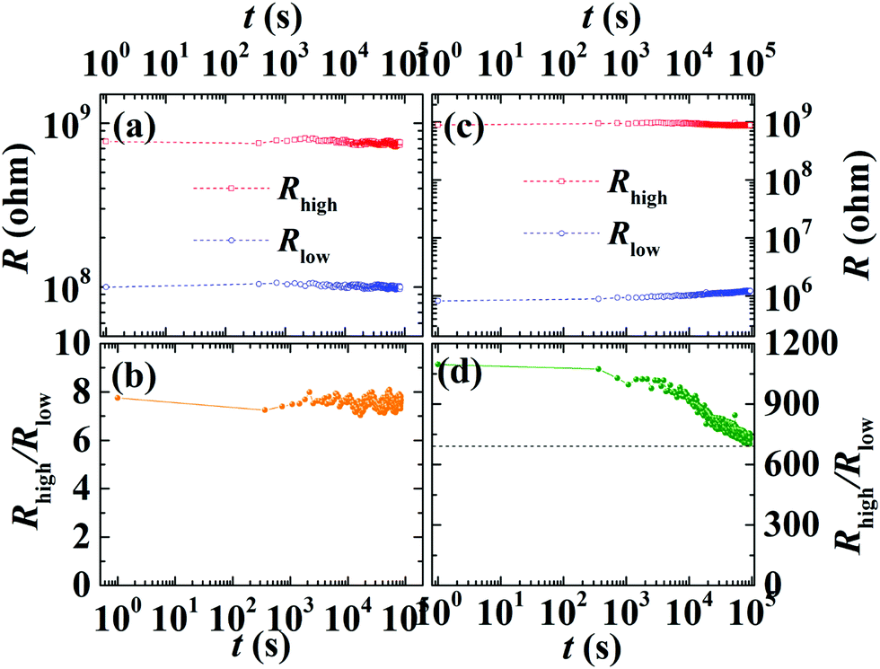 | ||
| Fig. 2 Retention characteristics of data written with pulses of different amplitudes and pulse widths (a and b) ±10 V and 100 ns, and (c and d) ±20 V and 1 ms. | ||
By applying voltage pulses of V = ±10 V (20 V) and τ = 100 ns (1 ms) to BFO devices, we tested the fatigue characteristics of the device, as shown in Fig. 3(a–d). RH and RL were evaluated by the current value at V = 0.3 V. Under a small voltage and short pulse, apart from a slight fluctuation, the switching ratio showed basically constant (>10) within the range of 103 switching cycles and remained as large as 8 even at 105 cycles, as shown in Fig. 3(a and b). This durability was better than that of previous switchable diodes.8,10 The switching-cycle dependence of RH/RL was similar to those of Pr,10 as shown in Fig. S2 (ESI†). The fatigue characteristics of switching ratios may be controlled by polarization fatigue under small voltages and short pulses. On the contrary, under a large voltage and long pulse, although a large switching ratio existed, the switching ratio greatly fluctuated owing to the instability of ion diffusion induced by Bi-vacancy defects, as shown in Fig. 3(c and d). For practical applications of ferroelectric memristors, the data retention and fatigue resistance should be improved. Further investigations on fatigue mechanism may provide clues to improving the device characteristics.
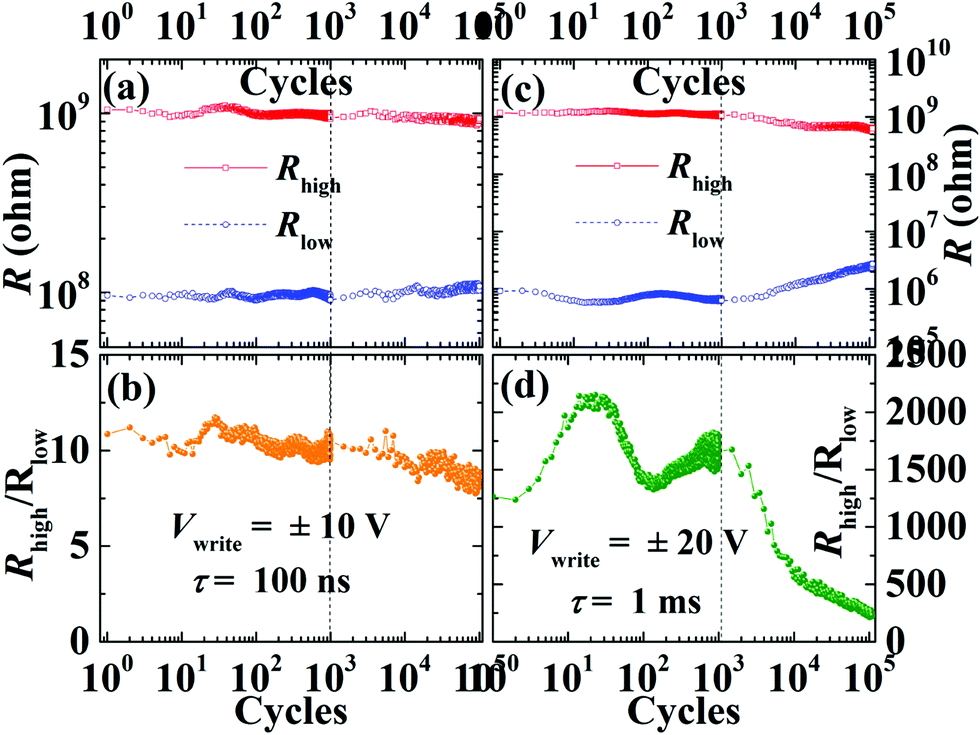 | ||
| Fig. 3 Fatige characteristics of BFO devices measured in pulsed-voltage mode with voltage pulses of (a and b) (±10 V, 100 ns) and (c and d) (±20 V, 1 ms). | ||
Two different RS mechanisms were found to exist in the same device. One mechanism was based on ferroelectricity, and the other was based on ion migration. Ferroelectricity can be excited by the coercive voltage, whereas a larger voltage was required for the ion migration that can be activated by low-frequency long pulses. Although the ion-migration mechanism had a large switching ratio, it showed great instability. For resistive switches based on ferroelectric properties, although the switch ratio was relatively small, it showed good retention performance and stability. Therese findings indicated the good application prospects of ferroelectric resistive devices.
As we all know, the part with large resistance in the conductive channel plays a decisive role in the total resistance. Therefore, the conductance mechanism is the origin of the resistance in the large-resistance part of the conductive channel. To further investigate the RS mechanism of ferroelectric devices, analysis on internal conductive-transport properties is necessary. The most likely conduction mechanisms include electrode/bulk interface-dominated mechanisms: Schottky emission (SE), and Fowler–Nordheim (FN) tunneling, and bulk-limited conduction mechanisms: space-charge-limited conduction (SCLC) and Poole–Frenkel emission (PF).41–43 We used the above models to analyze the data, as shown in the ESI† (Fig. S3 and S4). Results showed that under a large voltage, only the space-charge mechanism fitted the data perfectly, indicating that the migration of charged ions causes the restriction of space charge on the movement of carriers. At high voltages, we attributed the electrical-transport mechanism to the electroforming mechanism caused by ion migration. This finding was consistent with the mechanism of most oxides.5,7 To obtain stable ferroresistive devices, we should avoid applying voltage to the voltage required for electroforming. Under the DC small signal, we found the various electrical-transport mechanisms (SCLC, SE and PF) worked together and were coupled with each other. It shows that the contributions of the three mechanisms to the total resistance are not much different. In this case, the J–V characteristic can be controlled by artificially adjusting any one of the mechanisms. Here, the interfacial barrier (SE mechanism) was adjusted by the ferroelectric polarization to achieve the bipolar switching. In the following section, we focus on the regulation of the interfacial Schottky barrier (SE mechanism) by ferroelectric polarization and its effect on RS under low voltage. Further analysis based on the band theory was conducted.
In our BFO films, the volatilization of Bi introduced a Bi deficiency δ in the molecular formula of Bi1−δFeO3. The valence state of Fe ion changed with the introduction of holes by Bi volatilization. Given that the work functions of LSMO and Pt are ∼4.8 and ∼5.3 eV, respectively, and the electron affinity and band gap of BFO are ∼3.3 and ∼2.8 eV, respectively,44 The work function of the BFO is about 4.7 eV. BFO and LSMO not only have similar work functions, but also have matching lattice parameters. The BFO/LSMO interface is often regarded as an ohmic contact due to the negligible Schottky barrier between BFO and LSMO.28,33,45
A passive or dead layer, a very thin non-ferroelectric dielectric layer, is inevitable on the contact interface of a metal electrode and a ferroelectric oxide layer.46–48 The properties of the interfacial layer depend on the electrode material and the crystallinity at the interface.46,47,49 The dead layer presenting a disordered or defect aggregation state may suppress the ferroelectricity at the interface, and have a certain impact on the ferroelectric retention and fatigue resistance.46,47,50 Non-epitaxial metal electrodes may contribute to the formation and growth of an interfacial dead layer. In contrast, epitaxial oxide electrodes can effectively suppress the formation and growth of an interfacial dead layer.46,47,50 In our devices, the bottom electrode LSMO not only epitaxially grown on the STO substrate, but also had an epitaxial relationship with the BFO. The top electrode Pt was prepared by non-epitaxial sputtering technology. As shown in Fig. 4, at the non-epitaxial Pt/BFO interface, a dead layer formed and acted as a barrier layer for hole-carrier conduction. At the epitaxial LSMO/BFO interface, the dead layer also formed but its thickness may be expected to be much less than that of the nonepitaxial Pt/BFO interface. The contact resistance of the LSMO/BFO interface was much lower than that of the Pt/BFO interface due to that carriers can tunnel through ultra-thin barriers. This may also be one of the reasons why the epitaxial LSMO/BFO interface is often regarded as ohmic contact in the literature.28,33,45 Accordingly, our device presented a metal (M)/insulator (I)/p-type ferroelectric semiconductor (F)/I (ultra-thin)/M structure. Mayer et al. given the band diagram of the above structure, and discussed the RS characteristics of the structure.25 Here, we developed a M/I/F/I/semiconductor (S) model based on Mayer's theory25 to discuss the RS characteristics observed in our devices.
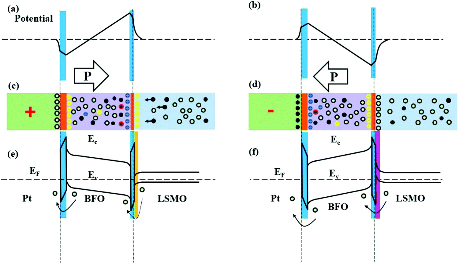 | ||
| Fig. 4 Potential distribution in BFO memristors for positive (a) and negative (b) ferroelectric polarization. Schematics showing the (c and d) charge distribution and (e and f) energy-band diagrams of the devices for positive and negative polarization, respectively. Hollow circle, hole; black dot, electron; yellow signal, negative bound charge or acceptor; blue signal, positive bound charge or donor; red signal, carriers captured by defects. | ||
The energy band diagrams of our device are shown in Fig. 4. We abbreviated the interfacial dead layer as IL. The potential profile at the interface changes significantly depending on the polarization direction, as shown in Fig. 4(a) and (b). Fig. 4(c, e) and (d, f) shows the charge distribution and energy-band diagrams of the device under positive and negative polarization, respectively. Because carriers can tunnel through the ultra-thin dead layer between LSMO and BFO. The influence of the LSMO/IL/BFO interface can be ignored. It is only necessary to pay attention to the band change at the Pt/IL/BFO interface. For downward polarization (Pt → LSMO), the upward bending of BFO band near the upper interface induced by the negative bound charges, enlarged the gap between the band of BFO and that of IL, and formed a depletion region near the interface, thus improving the effective barrier for hole-carrier conduction. The device exhibited a high resistance state. For upward polarization (LSMO → Pt), the downward bending of BFO band near the upper interface induced by the positive bound charges, reduced the gap between the band of BFO and that of IL, and formed an accumulation zone near the interface, thus decreasing the effective barrier for hole-carrier conduction. The device exhibited a low-impedance state. To set the resistance state or achieve SR switching, we only need to control the polarization direction by applying a voltage pulse. For example, the switching from HRS to LRS (set process) was to flip the polarization from downward to upward. This can be achieved by applying a positive voltage greater than the coercive field to the LSMO electrode. To switch from LRS to HRS (reset process), the polarization is reversed by applying a negative voltage pulse, thereby bending the band at the interface downward.
In this model, the interfacial and depletion layers acted as an effective barrier to the hole-carrier conduction at the Pt/IL/BFO interface. As shown in Fig. 4, the effective barrier in the downward polarization state was higher than that in the upward polarization state. The variable barrier height and width depending on the polarization directions controlled the hole-carrier conduction at the Pt/BFO interface, which was a possible mechanism of the RS effect at high frequencies.
3. Conclusions
Through CSD, we epitaxially fabricated LSMO and p-type BFO thin films on STO (001) single-crystal substrate in turn to fabricate BFO memristors. Using the device as a model system, we studied the ferroresistive and non-ferroresistive-switching behaviors of BFO device in terms of current–voltage measurements at different sweep voltages, sweep frequencies, and pulsed-voltage switching measurements. The devices showed bipolar RS with a zero-crossing hysteretic current–voltage characteristic. Under DC voltage, we observed that the electroforming behavior was driven by the large electric field. However, at high frequency (f = 1 kHz), positive and negative current peaks originating from ferroelectric displacement current were observed prior to set and reset switching processes, respectively. Our MIFS model told us that the modification of the potential profile of the barrier at the Pt/BFO interface induced by polarization reversal may be responsible for the RS phenomenon at high frequencies. In summary, the RS behavior of the BFO device originated from ferroelectric-polarization reversal at high frequencies or the defect electroforming process driven by a large electric field at low frequencies. The ferroelectricity-based retention (data retention > 105 s) and antifatigue (endurance > 105 cycles) properties of BFO devices were superior to those of electroforming processes based on redox reactions (103 s and 103 cycles). The current study explained the controversy over the origin of resistive switches in ferroelectric-oxide films for many years and showed promising characteristics for application in nonvolatile memories.4 Experimental section
Device fabrication
As a mature method for preparing polycrystalline oxide thin films, CSD has recently been used to fabricate epitaxial ferroelectric BFO thin films.51–54 The stability of epitaxial ferroelectric BFO films prepared by this method is even higher than that of MOCVD and PLD films.53–56 Here, the (00l) oriented BFO film and LSMO film electrode were epitaxially grown on (001) oriented STO substrate by CSD method. By electron-beam evaporation, a top electrode of Pt (200 μm in diameter) was deposited on the BFO layer through a shadow mask.Preparation of BFO films
Stoichiometric amounts of Bi(NO3)3·5H2O and Fe(NO3)3·9H2O were weighed and dissolved in a solvent mixture of 2-methoxyethanol and acetic acid to obtain a 0.25 M precursor solution. Under a nitrogen atmosphere with a humidity less than 10%, the sol films were spin-coated onto a clean and preheated (70 °C) substrate, first at 500 rpm for 5 s, then at 6000 rpm for 1 minute. The spin-coated samples were subjected to a low-temperature heat treatment at 90 °C for 10 minutes, and then at 270 °C for 5 minutes. The films were then sequentially heated by putting the samples in a tube furnace with oxygen atmosphere, pre-annealed at 450 °C for 30 minutes to pyrolysis, and annealed at 650 °C for 1 hour to crystallize. These coating and drying processes were repeated several times to achieve a thickness of about 100 nm.Preparation of LSMO films
Stoichiometric amounts of (CH3COOH)3La, (CH3COOH)2Mn and (CH3COOH)2Sr were weighed and dissolved in a solvent mixture of acetic acid and distilled water to obtain a 0.1 M precursor solution. Under ambient atmosphere with a humidity of 35–50%, the sol films were spin-coated onto a clean and preheated (70 °C) substrate, first at 500 rpm for 5 s, then at 7000 rpm for 1 minute. Subsequently, a crystallization treatment was performed in a tube furnace with oxygen atmosphere at 950 °C for 30 min to obtain the final film with a thickness of about 10 nm.Measurements
The crystalline structures of the prepared films were analyzed by a D/max-rA XRD system with Cu-Kα radiation (λ = 0.15406 nm). Ferroelectric properties were determined using an RT66A standard ferroelectric test system. Current–voltage measurements were performed using a semiconductor testing system (Keithley 4200-SCS).Conflicts of interest
There are no conflicts to declare.Acknowledgements
The work was supported in part by funding from the Natural Science Foundation of Shandong Province (No. ZR201702120113), National Natural Science Foundation of China (No. 11104116, 51372100, 51172094 and 51702120), and the Distinguished Middle-Aged and Young Scientist Encourage and Reward Foundation of Shandong Province (No. BS2011CL003).References
- L. Chua, Semicond. Sci. Technol., 2014, 29, 104001 CrossRef.
- P. Yao, H. Wu, B. Gao, J. Tang, Q. Zhang, W. Zhang, J. J. Yang and H. Qian, Nature, 2020, 577, 641 CrossRef CAS.
- D. Ielmini and H. S. P. Wong, Nat. Electron., 2018, 1, 333 CrossRef.
- M. Horowitz, 1.1 computing's energy problem (and what we can do about it). In 2014 IEEE International Solid-State Circuits Conference Digest of Technical Papers (ISSCC) (pp. 10–14). IEEE.
- R. Waser, R. Dittmann, G. Staikov and K. Szot, Adv. Mater., 2009, 21, 2632 CrossRef CAS.
- J. J. Yang, D. B. Strukov and D. R. Stewart, Nat. Nanotechnol., 2013, 8, 13 CrossRef CAS.
- D. Ielmini and R. e. Waser, Resistive Switching: From Fundamentals of Nanoionic Redox Processes to Memristive Device Applications, Wiley VCH, Weinheim, 2016 Search PubMed.
- T. Choi, S. Lee, Y. J. Choi, V. Kiryukhin and S.-W. Cheong, Science, 2009, 324, 63 CrossRef CAS.
- H. T. Yi, T. Choi, S. G. Choi, Y. S. Oh and S. W. Cheong, Adv. Mater., 2011, 23, 3403 CrossRef CAS.
- A. Q. Jiang, C. Wang, K. J. Jin, X. B. Liu, J. F. Scott, C. S. Hwang, T. A. Tang, H. B. Lu and G. Z. Yang, Adv. Mater., 2011, 23, 1277 CrossRef CAS.
- M. Zhuravlev, R. Sabirianov, S. Jaswal and E. Tsymbal, Phys. Rev. Lett., 2005, 94, 246802 CrossRef.
- V. Garcia, S. Fusil, K. Bouzehouane, S. Enouz-Vedrenne, N. D. Mathur, A. Barthélémy and M. Bibes, Nature, 2009, 460, 81 CrossRef CAS.
- D. Pantel, S. Goetze, D. Hesse and M. Alexe, Nat. Mater., 2012, 11, 289 CrossRef CAS.
- P. Maksymovych, S. Jesse, P. Yu, R. Ramesh, A. Baddorf and S. Kalinin, Science, 2009, 324, 1421 CrossRef CAS.
- A. Chanthbouala, A. Crassous, V. Garcia, K. Bouzehouane, S. Fusil, X. Moya, J. Allibe, B. Dlubak, J. Grollier, S. Xavier, C. Deranlot, A. Moshar, R. Proksch, N. D. Mathur, M. Bibes and A. Barthélémy, Nat. Nanotechnol., 2012, 7, 101 CrossRef CAS.
- Y. W. Yin, J. D. Burton, Y. M. Kim, A. Y. Borisevich, S. J. Pennycook, S. M. Yang, T. W. Noh, A. Gruverman, X. G. Li, E. Y. Tsymbal and Q. Li, Nat. Mater., 2013, 12, 397 CrossRef CAS.
- A. Q. Jiang, W. P. Geng, P. Lv, J.-W. Hong, J. Jiang, C. Wang, X. J. Chai, J. W. Lian, Y. Zhang, R. Huang, D. W. Zhang, J. F. Scott and C. S. Hwang, Nat. Mater., 2020 DOI:10.1038/s41563-020-0702-z.
- P. Sharma, Q. Zhang, D. Sando, C. H. Lei, Y. Liu, J. Li, V. Nagarajan and J. Seidel, Sci. Adv., 2017, 3, e1700512 CrossRef.
- D. S. Rana, I. Kawayama, K. Mavani, K. Takahashi, H. Murakami and M. Tonouchi, Adv. Mater., 2009, 21, 2881 CrossRef CAS.
- P. W. Blom, R. M. Wolf, J. F. Cillessen and M. P. Krijn, Phys. Rev. Lett., 1994, 73, 2107 CrossRef CAS.
- Y. Watanabe, Appl. Phys. Lett., 1995, 66, 28 CrossRef CAS.
- A. Bune, S. Ducharme, V. Fridkin, L. Blinov, S. Palto, N. Petukhova and S. Yudin, Appl. Phys. Lett., 1995, 67, 3975 CrossRef CAS.
- K. Gotoh, H. Tamura, H. Takauchi and A. Yoshida, Jpn. J. Appl. Phys., 1996, 35, 39 CrossRef CAS.
- S. Y. Wu, H. Liu, L. Gu, R. Singh, L. Budd, M. Van Schilfgaarde, M. McCartney, D. J. Smith and N. Newman, Appl. Phys. Lett., 2003, 82, 3047 CrossRef CAS.
- R. Meyer, J. R. Contreras, A. Petraru and H. Kohlstedt, Integr. Ferroelectr., 2004, 64, 77 CrossRef CAS.
- D. Lee, S. H. Baek, T. H. Kim, J. G. Yoon, C. M. Folkman, C. B. Eom and T. W. Noh, Phys. Rev. B: Condens. Matter Mater. Phys., 2011, 84, 125305 CrossRef.
- C. Wang, K.-J. Jin, Z.-T. Xu, L. Wang, C. Ge, H.-B. Lu, H.-Z. Guo, M. He and G.-Z. Yang, Appl. Phys. Lett., 2011, 98, 192901 CrossRef.
- D. Chen, A. Li and D. Wu, J. Mater. Sci.: Mater. Electron., 2014, 25, 3251 CrossRef CAS.
- A. Tsurumaki, H. Yamada and A. Sawa, Adv. Funct. Mater., 2012, 22, 1040 CrossRef CAS.
- H. Yang, H. M. Luo, H. Wang, I. O. Usov, N. A. Suvorova, M. Jain, D. M. Feldmann, P. C. Dowden, R. F. DePaula and Q. X. Jia, Appl. Phys. Lett., 2008, 92, 102113 CrossRef.
- S. Hong, T. Choi, J. H. Jeon, Y. Kim, H. Lee, H. Y. Joo, I. Hwang, J. S. Kim, S. O. Kang and S. V. Kalinin, Adv. Mater., 2013, 25, 2339 CrossRef CAS.
- D. Jiménez, E. Miranda, A. Tsurumaki-Fukuchi, H. Yamada, J. Suñé and A. Sawa, Appl. Phys. Lett., 2013, 103, 263502 CrossRef.
- L. Fang, L. You, Y. Zhou, P. Ren, Z. Shiuh Lim and J. Wang, Appl. Phys. Lett., 2014, 104, 142903 CrossRef.
- Q. Man, W. Sun, F. Yang, C. Qiu, Y. Zhao and G. Hu, J. Mater. Sci.: Mater. Electron., 2014, 25, 1269 CrossRef CAS.
- J. Wang, J. B. Neaton, H. Zheng, V. Nagarajan, S. B. Ogale, B. Liu, D. Viehland, V. Vaithyanathan, D. G. Schlom, U. V. Waghmare, N. A. Spaldin, K. M. Rabe, M. Wuttig and R. Ramesh, Science, 2003, 299, 1719 CrossRef CAS.
- F. Yang, M. H. Tang, Y. C. Zhou, X. J. Zheng, F. Liu, J. X. Tang, J. J. Zhang and J. Zhang, Appl. Phys. Lett., 2007, 91, 142902 CrossRef.
- J. Park, S. Baek, P. Wu, B. Winchester, C. Nelson, X. Pan, L. Chen, T. Tybell and C. Eom, Appl. Phys. Lett., 2010, 97, 212904 CrossRef.
- G. Zhou, S. Duan, P. Li, B. Sun, B. Wu, Y. Yao, X. Yang, J. Han, J. Wu, G. Wang, L. Liao, C. Lin, W. Hu, C. Xu, D. Liu, T. Chen, L. Chen, A. Zhou and Q. Song, Adv. Electron. Mater., 2018, 4, 1700567 CrossRef.
- Y. Yu, C. Wang, C. Jiang, I. Abrahams, Z. Du, Q. Zhang, J. Sun and X. Huang, Appl. Surf. Sci., 2019, 485, 222 CrossRef CAS.
- D. S. Jeong, R. Thomas, R. Katiyar, J. Scott, H. Kohlstedt, A. Petraru and C. S. Hwang, Rep. Prog. Phys., 2012, 75, 076502 CrossRef.
- F. Yang, F. Zhang, G. Hu, Z. Zong and M. Tang, Appl. Phys. Lett., 2015, 106, 172903 CrossRef.
- T. Fujii, M. Kawasaki, A. Sawa, Y. Kawazoe, H. Akoh and Y. Tokura, Phys. Rev. B: Condens. Matter Mater. Phys., 2007, 75, 165101 CrossRef.
- A. Odagawa, H. Sato, I. Inoue, H. Akoh, M. Kawasaki, Y. Tokura, T. Kanno and H. Adachi, Phys. Rev. B: Condens. Matter Mater. Phys., 2004, 70, 224403 CrossRef.
- S. J. Clark and J. Robertson, Appl. Phys. Lett., 2007, 90, 132903 CrossRef.
- Y. Zhou, X. Zou, L. You, R. Guo, Z. Shiuh Lim, L. Chen, G. Yuan and J. Wang, Appl. Phys. Lett., 2014, 104, 012903 CrossRef.
- T. Nakamura, Y. Nakao, A. Kamisawa and H. Takasu, Appl. Phys. Lett., 1994, 65, 1522 CrossRef CAS.
- J. Cillessen, M. Prins and R. Wolf, J. Appl. Phys., 1997, 81, 2777 CrossRef CAS.
- Z. Zhong, Y. Sugiyama and H. Ishiwara, Jpn. J. Appl. Phys., 2008, 47, 6448 CrossRef CAS.
- C. B. Eom, R. B. V. Dover, J. M. Phillips, D. J. Werder, J. H. Marshall, C. H. Chen, R. J. Cava, R. M. Fleming and D. K. Fork, Appl. Phys. Lett., 1993, 63, 2570 CrossRef CAS.
- F. Yang, M. H. Tang, Y. C. Zhou, F. Liu, Y. Ma, X. J. Zheng, J. X. Tang, H. Y. Xu, W. F. Zhao, Z. H. Sun and J. He, Appl. Phys. Lett., 2008, 92, 022908 CrossRef.
- Q. Zhang, N. Valanoor and O. Standard, J. Mater. Chem. C, 2015, 3, 582 RSC.
- S. K. Singh, Y. K. Kim, H. Funakubo and H. Ishiwara, Appl. Phys. Lett., 2006, 88, 162904 CrossRef.
- P. Machado, M. Scigaj, J. Gazquez, E. Rueda, A. Sanchez-Diaz, I. Fina, M. Gibert-Roca, T. Puig, X. Obradors, M. Campoy-Quiles and M. Coll, Chem. Mater., 2019, 31, 947 CrossRef CAS.
- F. Liu, F. Q. Ji, Y. L. Lin, S. F. Huang, X. J. Lin and F. Yang, ACS Appl. Nano Mater., 2020 DOI:10.1021/acsanm.0c01649.
- S. Yasui, K. Nishida, H. Naganuma, S. Okamura, T. Iijima and H. Funakubo, Jpn. J. Appl. Phys., 2007, 46, 6948 CrossRef CAS.
- H. Hojo, K. Onuma, Y. Ikuhara and M. Azuma, Appl. Phys. Express, 2014, 7, 091501 CrossRef.
Footnote |
| † Electronic supplementary information (ESI) available. See DOI: 10.1039/d0ma00488j |
| This journal is © The Royal Society of Chemistry 2020 |