
 Open Access Article
 This Open Access Article is licensed under a Creative Commons Attribution-Non Commercial 3.0 Unported Licence
Pyrene-functionalized tungsten disulfide as stable resistive photosensor†
Ruben
Canton-Vitoria
*a,
Sebastian
Nufer
bc,
Xiaoyang
Che
de,
Yuman
Sayed-Ahmad-Baraza
 d,
Raul
Arenal
*fgh,
Carla
Bittencourt
*i,
Adam
Brunton
b,
Alan B.
Dalton
c,
Christopher P.
Ewels
*d and
Nikos
Tagmatarchis
*a
d,
Raul
Arenal
*fgh,
Carla
Bittencourt
*i,
Adam
Brunton
b,
Alan B.
Dalton
c,
Christopher P.
Ewels
*d and
Nikos
Tagmatarchis
*a
aTheoretical and Physical Chemistry Institute, National Hellenic Research Foundation, 48 Vassileos Constantinou Avenue, 116 35 Athens, Greece. E-mail: tagmatar@eie.gr
bM-Solv Ltd, Oxonian Park, Langford Locks, Kidlington, Oxford, OX5 1FP, UK
cDepartment of Physics, University of Sussex, Brighton, BN1 9R, UK
dInstitut des Materiaux Jean Rouxel (IMN), UMR6502 CNRS, Universite de Nantes, 2 Rue de la Houssiniere, BP32229, 44322, Nantes, France
eCentre de Recherche Paul Pascal (CRPP)-UMR5031, 115 Avenue du Dr Albert Schweitzer, 33600 Pessac, France
fLaboratorio de Microscopias Avanzadas (LMA), Universidad de Zaragoza, Calle Mariano Esquillor, 50018 Zaragoza, Spain
gFundacion ARAID, 50018 Zaragoza, Spain
hInstituto de Nanociencia y Materiales de Aragón (INMA), CSIC-Universidad de Zaragoza, Calle Pedro Cerbuna, 50009 Zaragoza, Spain
iChimie des Interactions Plasma-Surface, University of Mons, 20 Place du Parc, 7000 Mons, Belgium
First published on 22nd September 2020
Abstract
Pyrene carrying an 1,2-dithiolane linker was employed to functionalize exfoliated WS2 and the resulting material was used in a proof-of-concept application as a photoresistor type sensor. The WS2–pyrene hybrid material was comprehensively characterized by spectroscopic, thermal and microscopy techniques, coupled to density functional theory modelling. The high solubility of the WS2–pyrene hybrid material allows easy manipulation in wet media, making it suitable for device fabrication. Thus, a two-terminal resistive photosensor was developed and tested for photodetection. The photosensitivity of WS2 was improved by the presence of covalently attached pyrene by a factor of 2–3, the response linearly dependent on light intensity. Device reaction time was also improved, and critically the photosensor stability was significantly enhanced. Functionalization of exfoliated WS2 material heals vacancies, oxidation and other damage sites liable to impede photoelectric response. This proof-of-concept study opens the way for incorporation of diverse chromophores active in the visible and/or NIR region of the electromagnetic spectrum to WS2 in order to stabilise it and broaden its photoresistive sensing applicability.
Introduction
The combination of high area-to-volume ratio with band gaps in the visible region makes transition metal dichalcogenides (TMDs) attractive for energy and sensing applications.1–4 Depending on the process used, exfoliation of tungsten disulfide WS2 gives either semiconducting or metallic nanosheets.5–10 Functionalizing these improves their marginal dispersibility in wet media, and can additionally impart new functionality. For example, WS2 nanosheets functionalized with positively charged ammonium moieties have been used to electrostatically couple to negatively charged photoactive species such as derivatized porphyrins,11 carbon nanodots12 and a water-soluble polythiophene.13 In these cases, functionalization is achieved through addition of 1,2-dithiolanes to exfoliated WS2, rationalized by the high binding affinity of sulfur for tungsten atoms. Precisely, 1,2-dithiolanes efficiently bind at the edges of WS2 layers, where sulfur vacant sites are numerous in comparison with those in the basal plane. A similar methodology has also been employed to directly incorporate pyrene,14 carbon nanodots,15 phthalocyanine16 and porphyrin17 species onto TMDs via robust and stable bond formation. The resulting electron donor–acceptor hybrid systems are important in electrocatalytic processes and photoinduced charge-transfer phenomena.Semiconductor resistive photosensors operate through a reduction of electrical resistance under illumination, with light whose energy is close to the semiconductor band gap. Key requirements are high surface area, sub-nanometric thickness, and a controllable band gap within the solar irradiation region. TMDs are candidates for nanoscale photosensing, potentially replacing silicon and other materials.18 Amongst these, nanosized WS2 shows the fastest light-response19–21 and has excellent carrier mobility, high photoelectrical on/off ratio and stability, with excitons in the visible region of the electromagnetic spectrum.22–26 However, stability of TMDs over time is a limiting factor.27,28 Thus, improving the WS2 sensitivity, signal/noise, response time and stability is strongly desired for real sensing applications.
Heterostructures based in WS2 with e.g. graphene, show excellent results, sharply enhancing sensitivity, however, their realization requires tedious engineering technology with individual design of electrodes, handicapping any scalable production.29 On the other hand, functionalization of 2D nanostructures allows the realization of material in bulk quantities with robust properties, suitable for technological applications. Focusing on the development of light sensors, functionalization of WS2 with Au nanospheres strongly enhanced the sensitivity of CVD grown WS2 at 590 nm and 740 nm, however with a slow speed response of 3 s.30 Functionalization with carbon nanotubes improved the response up to 0.003 μs at 633 and 875 nm, and in addition, resulted in fourfold enhancement of the photo-response.31 Incorporation of polyimide into WS2 resulted in flexible devices with 10-fold sensitivity increase and a fast response of 500 μs.32 Functionalization of exfoliated WS2 with n-doped Si heterojunctions also has a 10-fold current change once a 633 nm laser pulse was applied, with the response lifetime dependent on the applied bias voltage.33 An excellent enhancement of photo-response (1000× at 532 nm) was also found upon interfacing WS2 with graphene oxide nanoparticles, however, the noise/response enhanced proportionally, and response time decreased around 10 times.34 Functionalization of WS2 with nanocrystals of SnSe enhanced the photo-response ratio to the NIR (1062 nm) and the sensitivity by 1 or 2 orders of magnitude, however, the fast response decreased to half.35 Functionalization of WS2 with black phosphorous nanosheets36 improved the photo-response, however, with the disadvantage of decreasing the fast response. Overall, despite some studies shown enhancement of the stability after functionalization, lack of reference WS2 makes difficult to draw reliable conclusions on thermal, electronic or chemical stability.
Photosensing evaluation of hybrid materials featuring organic dyes covalently incorporated on WS2 that participate in light-induced photophysical events has yet to be performed. Herein, we report on the functionalization of exfoliated WS2 with a pyrene modified 1,2-dithiolane derivative, followed by assessment of the resultant hybrid material as a stable resistive photosensor. We develop an easy and scalable two-terminal resistive photosensor with the pyrene-modified WS2 and find photoinduced sensitivity enhancement from the pyrene species to the conduction band of WS2. In addition, the WS2–pyrene based prototype device shows long term stability, rationalized by considering healing of defective sulfur sites by the covalent 1,2-dithiolane addition. The current study provides valuable information related to the electronic character of the hybrid material, understanding its resistive photosensing behavior and will allow systematic exploitation of its capabilities.
Results and discussion
Bulk WS2 was exfoliated to semiconducting nanosheets through chlorosulfonic acid treatment following an experimental procedure developed in our labs.5 The general scheme for the functionalization process is illustrated in Fig. 1. In a typical reaction, treatment of exfoliated WS2 with an excess of 1,2-dithiolane derivative 1 produces pyrene-modified WS2-based hybrid material 2. Filtration over PTFE membrane (0.2 μm pore size), followed by washing with dichloromethane, ensured that 2 was free from organic impurities and guaranteed the absence of any physisorbed pyrene species. In order to confirm the absence of physisorbed pyrene species, a control experiment, in which pyrene was simply mixed with exfoliated WS2, was conducted. Then, the mixture was filtered over PTFE membrane (0.2 μm pore size) and the solid material obtained was further washed with dichloromethane. This process indeed removed all physisorbed pyrene from WS2 as confirmed by the absence of pyrene features in the IR, UV-Vis and PL emission spectra.37 Hybrid material 2 forms stable dispersions in DMF, isopropanol and methanol without significant precipitation (even for several months). The dispersibility of 2 in those solvents allows easier manipulation and processing e.g. fabrication of devices by drop-casting processes en route the development of active electrodes. The molar absorptivity of hybrid 2 in DMF was found to be 434 L g−1 m−1 at 480 nm. In contrast, the dispersibility of 2 in solvents such as o-DCB, THF and dichloromethane was marginal.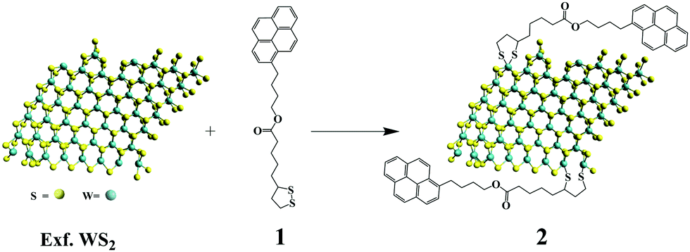 | ||
| Fig. 1 Functionalization of exfoliated WS2 with pyrene 1,2-dithiolane derivative 1 forming WS2–pyrene hybrid material 2. | ||
Attenuated-total-reflectance infra-red (ATR-IR) spectroscopy confirms the successful functionalization. Briefly, vibrations due to the presence of the carbonyl ester moiety at 1730 cm−1 and strong C–H stretching vibrations at 2950 cm−1 were identified for hybrid material 2 (Fig. 2a). Similar IR vibrations were found in the spectrum of 1,2-dithiolane derivative 1. Thermogravimetric analysis (TGA) allows estimating the degree of functionalization in hybrid material 2. Exfoliated WS2 is thermally stable up to at least 800 °C under nitrogen atmosphere. However, 2 showed a mass loss of 4.4% in the temperature range 250–550 °C (Fig. 2b), associated with thermal decomposition of the organic moieties covalently anchored on WS2. This mass loss corresponds to one pyrene unit for every 41 WS2 units within hybrid material 2.
 | ||
| Fig. 2 (a) ATR-IR spectra for pyrene derivative 1 (red) and hybrid material 2 (black). (b) Thermographs for exfoliated WS2 (gray) and hybrid material 2 (black), obtained under nitrogen atmosphere. (c) Raman spectra for exfoliated WS2 (gray) and hybrid material 2 (black), obtained upon 514 nm excitation. | ||
Resonant Raman spectra were obtained upon excitation at 514 nm. In both exfoliated WS2 and hybrid material 2, modes due to the 2LA(M), E12g, and A1g are visible at 350, 354 and 419 cm−1, respectively. However, the intensity of the defective mode 2LA(M) is significantly reduced for hybrid material 2 compared to exfoliated WS2 (Fig. 2c), suggesting that defects are reduced as functionalization occurs at sulfur-defect sites.
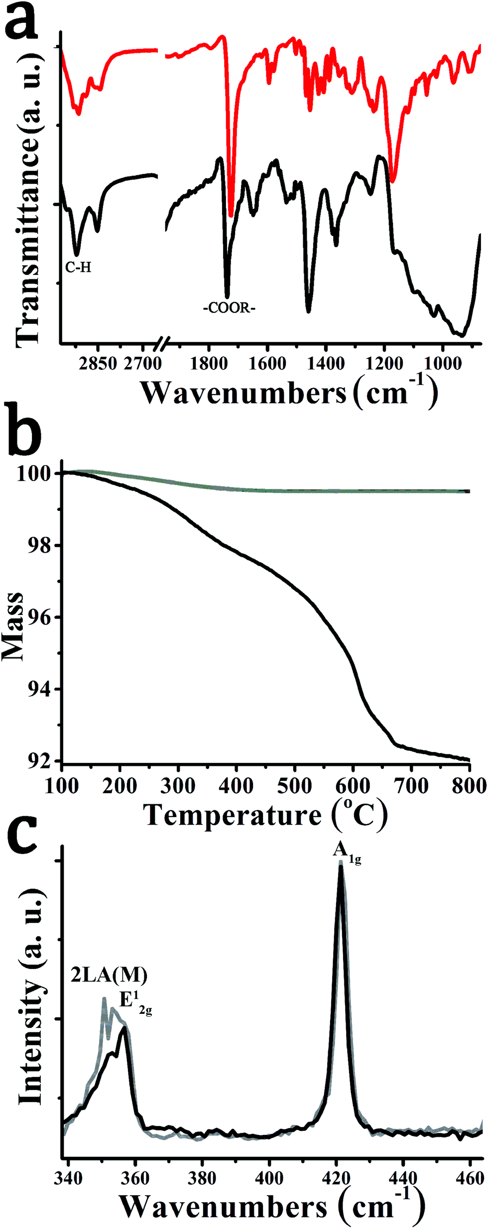
This can be further explored using X-ray photoelectron spectroscopy (XPS) of the W 4f and S 2p XPS core level spectra (Fig. 3). The energy positions of the doublet components S 2p3/2 and S 2p1/2 at 163.7 and 162.5 eV, respectively, and of W f5/2 and W f7/2 at 35.1 and 32.9 eV, respectively, indicate a W valence of +4 and a pure hexagonal phase of exfoliated WS2. The atomic ratio S/W estimated for exfoliated WS2 and pyrene modified WS2 hybrid material 2 is 1.75 and 1.95 (Fig. 3), i.e. corresponding to non-stoichiometric surface concentrations of WS1.75 and WS1.95, respectively. This demonstrates that sulfur vacancies are created during the exfoliation process, which are ‘reduced’ upon functionalization with pyrene derivative 1via interactions of the 1,2-dithiolane unit with the sulfur vacant sites. This WS2 restoration process during functionalization is also seen in an XPS doublet at 38.3 eV and 36.1 eV corresponding to residual WO3. After functionalization, the relative intensity of this doublet decreases from 4% to 2% of the total W 4f core level and shifts 0.2 eV towards low binding energy. Such shift is in concordance with other chromophores functionalized TMDs, and it is related with charge transfer interaction between the surface assembled chromophores and WS2.38
 | ||
| Fig. 3 The W 4f core levels of (a) exfoliated WS2, and (c) WS2–pyrene hybrid 2, reproduced using a component at 38.7 eV generated by photoelectrons emitted from W 5p3/2 in WS2 and two doublets W f5/2 and W f7/2, a high intensity one (35.1 eV and 32.9 eV) belonging to hexagonal WS2 and a low intensity one (38.3 eV and 36.1 eV) to WO3. The S 2p core levels are composed of a doublet (S 2p3/2 and S 2p1/2) at (b) 163.7 eV for exfoliated WS2, and (d) 162.5 eV for WS2–pyrene hybrid material 2. | ||
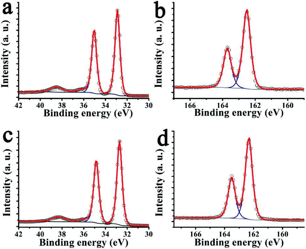
The stoichiometry change proposed by XPS corresponds to a higher functionalization degree than suggested from the TGA data. Since XPS is highly surface sensitive, this suggests that the material is not monolayer but contains also multi-layer flakes and particles. This is confirmed via high-resolution scanning TEM (Fig. 4a–c), where it can be seen that typical material indeed contains multi-layer flakes. This can actually be an advantage in terms of improved optical absorption for photoresistivity, as discussed further below. Electron energy-loss spectroscopy (EELS) confirms that pyrene is present ubiquitously across the flakes, see Fig. 4c, although its distribution is not homogenous. An EELS spectrum-line (SPLI) has been collected following the green marked line (Fig. 4c). Three different EEL spectra (marked as (i) to (iii)) have been selected from this SPLI and are displayed in Fig. 4d. S-L3,2 edge from WS2 can be observed in the three spectra. In the red EEL spectrum (ii), the C-K edge associated to pyrene is visible. From the analysis of the fine structures near of the edge (ELNES), this C-K edge is clearly different to this one from amorphous carbon,39–41 confirming the presence of pyrene.
 | ||
| Fig. 4 (a–c) High-angle annular dark-field (HAADF) high-resolution scanning transmission electron micrographs of typical WS2–pyrene hybrid 2. (c) An EELS SPLI has been collected following the green line marked in this HAADF image. (d) Three EEL spectra corresponding each of them to the sum of four EEL spectra collected in each of these highlighted areas (i)–(iii) are depicted in (d). | ||
We turn next to the optical response of the material. The electronic absorption spectrum of exfoliated WS2 as well as of hybrid material 2 is governed by characteristic bands attributed to the semiconducting phase of WS2, namely, the A excitonic band centered at 645 nm, the indirect excitonic B band at 545 nm, and two optical transitions associated with the density of states at 480 and 420 nm, suggesting a 340 nm average flake diameter and flakes with an average of 4 layers.42 Additional bands directly derived from the optical absorption of pyrene in hybrid material 2 are also discernable at 325 and 340 nm (Fig. 5a). In general, the UV-Vis spectrum of 2 is a simple superimposition of the absorption spectra of exfoliated WS2 and pyrene derivative 1, implying marginal, if any, electronic interactions between the two species at the ground state. However, the presence of pyrene moieties in hybrid material 2 guarantees more efficient absorption in the visible region in comparison with exfoliated WS2, suggesting an improvement of the response when employed as photo-resistive sensor (see below).
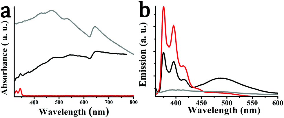 | ||
| Fig. 5 (a) UV-Vis spectra and (b) photoluminescence spectra (λexc 340 nm), for pyrene derivative 1 (red), exfoliated WS2 (gray) and hybrid material 2 (black), obtained in DMF. | ||
In sharp contrast, intimate electronic communication between pyrene and WS2 is visible in 2 at the excited state upon photoillumination at 340 nm. Specifically, based on steady-state photoluminescence assays, the characteristic emission bands of pyrene in derivative 1, centered at 375 and 395 nm, were substantially quenched by WS2 in hybrid material 2 (Fig. 5b), for samples possessing equal optical concentration at the excitation wavelength. This is to say that intra-hybrid transduction of energy from the singlet excited state of pyrene to WS2 takes place in 2. It should be noted that the broad feature at 490 nm observed in the photoluminescence spectrum of 2 is due to the pyrene excimer and should not be confused with impurity or WS2 exciton features. In fact, excimer formation in hybrid 2 can be considered as an additional electronic interaction between WS2 and pyrene, probably due to a favorable molecular orientation of pyrene onto the WS2 nanosheets.
These interactions can be explored further via density functional theory (DFT) calculations of a pristine pyrene moiety over the surface of WS2 (unit cell shown in ESI,† Fig. S1). The calculations show very strong binding (81.2 kcal mol−1) to the surface, with the pyrene only stable in a surface-parallel configuration (other orientations relaxing spontaneously to the parallel case, see Supplementary Movie M1, ESI†). The projected density of electronic states (PDOS) shows strong interaction between monolayer WS2 and pyrene (Fig. 6a). In comparison to isolated pyrene (Fig. 6b), the hybrid system shows an upshift in pyrene electronic states. Additionally, while the highest occupied molecular orbital (HOMO) remains sharp and localized, there is a strong broadening of the pyrene lowest-occupied molecular orbital (LUMO) and LUMO+1 states, where they couple strongly with electronic states in the neighbouring WS2 (Fig. 6a). This strong coupling confirms that HOMO–LUMO and HOMO–(LUMO+1) excitations in the pyrene will rapidly transfer to the conduction band of the underlying WS2, resulting in the observed quenching of the emission bands of pyrene. Given the difference in electronic behavior of mono- and multi-layer WS243 we also calculated the PDOS for pyrene on bilayer WS2 (ESI,† Fig. S1), where similar coupling is once again observed.
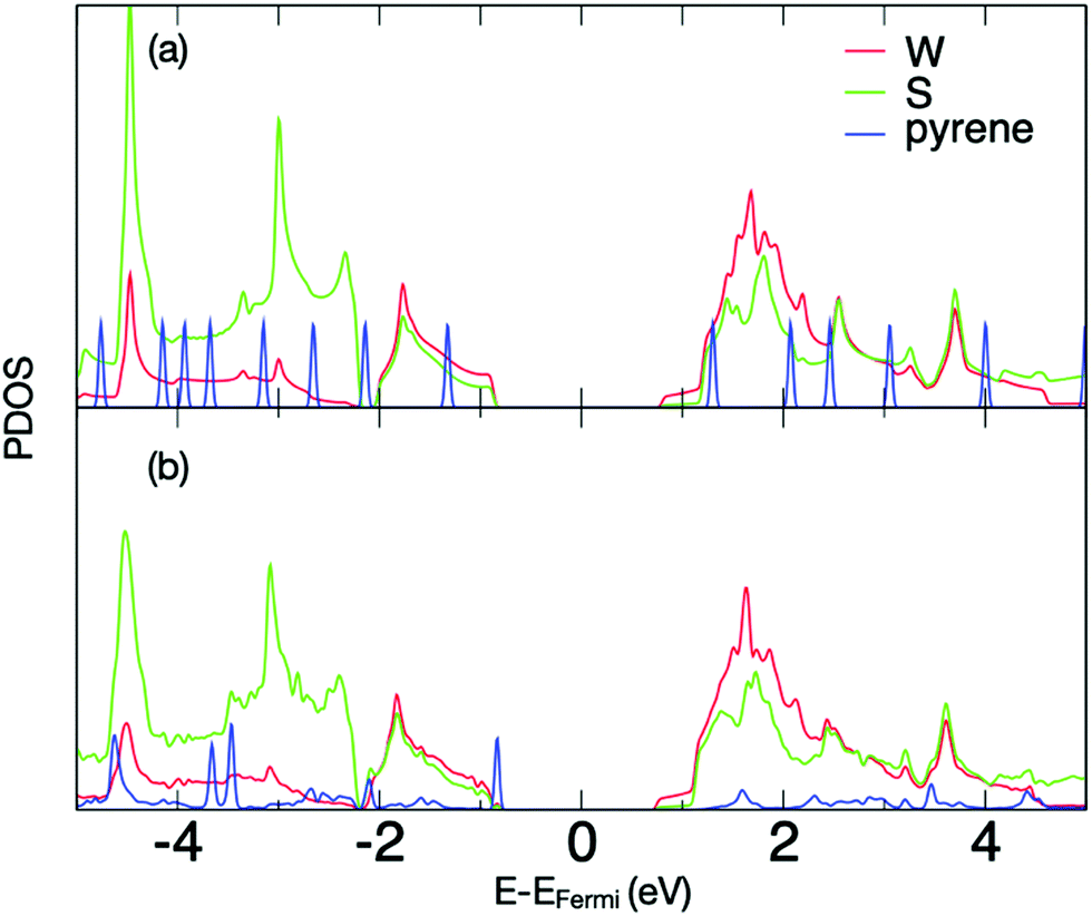 | ||
| Fig. 6 DFT calculated projected density of electronic states for (a) monolayer-WS2 and pyrene at infinite separation, (b) pyrene on monolayer WS2 surface in ground state configuration. Energies are shifted to place the Fermi level at 0 eV in each case, states localized on W/S/pyrene are marked in red/green/blue, respectively. | ||
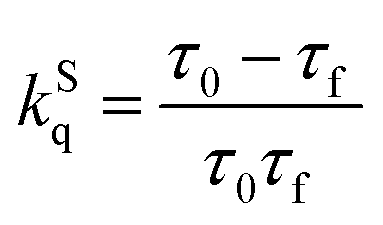
In order to understand further the phenomena occurring at the excited states, time-resolved photoluminescence assays were performed and the fluorescence lifetime based on the time-correlated-single-photon-counting method was determined. The emission decay of pyrene derivative 1 could be mono-exponentially fitted with a long lifetime of 3.78 ns (ESI,† Fig. S2). However, the emission decay of hybrid material 2 consists of two components with lifetimes of 0.22 and 3.79 ns. The fast 0.22 ns component is assigned to charge and/or energy transfer from pyrene to WS2 in accordance with the steady-state photoluminescence quenching results, and is consistent with the strong coupling observed in the DFT results. Based on eqn (1) and (2), the quenching rate constant kSq for the singlet excited state of 2 was evaluated as 4.28 × 10⁻⁹ s−1 and its quantum yield ΦSq was calculated to be 0.94.
 | (1) |
| ΦSq = KSqτf | (2) |
Next, several prototype devices of WS2–pyrene hybrid material 2 were fabricated and tested as resistive photosensors and compared to exfoliated WS2. The sensor consists of 700 nm-thick metallic molybdenum interdigitated electrodes on a glass substrate (∼100 cm2), with exfoliated WS2 or WS2–pyrene material 2 drop-cast. The devices are very sensitive to changes in the atmosphere produced by different solvents such as isopropanol, NH3 or water. For example, moisture produces strong changes with time-response of several hours, since desorption needs long time at room temperature and causes a drift that can be wrongly attributed to the degradation of the material. Hence, to abolish such undesired interactions, the devices were isolated from their environment using a layer of transparent Scotch tape (full details are given at the Experimental section). The effect of moisture as well as pulsed light irradiation on exfoliated WS2 and WS2–pyrene material 2 with and without the Scotch tape is presented at the ESI,† Fig. S3. The material morphology (ESI,† Fig. S4) shows that both WS2 and WS2–pyrene material 2 consist of a homogeneous distribution of small agglomerate flakes that fully cover the integrated electrodes.
Fig. 7 shows the resistance response of representative photosensors to white light irradiation at constant temperature. Exfoliated WS2 shows a small resistance change caused by photoexcitation of carriers in the semiconductor, which is weakly proportional to the light intensity (Fig. 7a). Sample resistance increases gradually over time and additionally the device shows significant drift, which is clearer in exposure measurements taken over several minutes (Fig. 7b). Both of these effects can be ascribed to thermal and photoinduced degradation. Considering next the WS2–pyrene hybrid material 2 under light irradiation, electron transfer additionally occurs from pyrene to the semiconducting WS2 nanosheets, shifting the Fermi level and decreasing the device resistance. This can be seen in Fig. 7a where the resistance response is enhanced by typically 2–3 times over that of exfoliated WS2. In this case, the resistance drop is strongly proportional to light intensity. Additionally, in this case the device maintains a stable baseline during and after long-time exposure pulse (Fig. 7b) and shows reproducible sensitivities at equivalent pulse measurements (ESI,† Fig. S5). This is in concordance with a recent study in which pyrene was shown to enhance the stability of TMDs under air, moisture and solar light irradiation by years.37
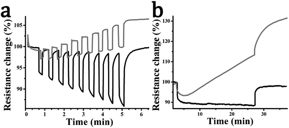 | ||
| Fig. 7 Resistance response of hybrid material 2 (black) and exfoliated WS2 (gray) with (a) increasing light irradiation from 400 to 1200 mW cm−2 with 10 s light pulses every 20 s, and (b) light irradiation with a continuous 25 min pulse with an intensity of 600 mW cm−2 showing baseline drift in the exfoliated WS2 (gray) which is eliminated in the hybrid material 2 (black). | ||
The response-lifetimes for exfoliated WS2 can be fitted using a single exponential with time constant of 77.8 s. Material 2 however requires a biexponential fit. The longest time constant, accounting for 26% of the signal, is somewhat shortened to 39.0 s, possibly due to changes in the material (vacancy healing) induced by the functionalisation. However the majority (73%) of the response comes from a new ultra-rapid response associated with photo-excited pyrene charge carriers. The time constant is fitted at 0.37 s but is limited by the temporal resolution of the experiment (one data point per 0.5 s) and thus represents an upper bound. We note that the relative contributions are consistent with the enhancement in resistance response we observe being attributable to the rapid pyrene optical response. The recovery response behaviour is similar, with mono-exponential time constant of 76.1 s for the exfoliated WS2 and time constants of 80.7 and 0.90 s for material 2 with bi-exponential fit. Response and response-recovery data and fit data are given at ESI,† Fig. S6 and Table S1.
Conclusions
We successfully synthesized and characterized the covalently modified WS2–pyrene hybrid material 2 based on the addition of pyrene-modified 1,2-dithiolane species on exfoliated WS2. Then, the hybrid material 2 was employed in a proof-of-concept application as resistive photosensor, whose response was found to be linearly dependent on light intensity. There are a number of clear benefits that arise from the particular 1,2-dithiolane functionalization of WS2. Firstly, the functionalisation improved the quality of the host nanoflake WS2 material itself, largely restoring its WS2 stoichiometry and reducing the number of vacancies, oxidation and other damage sites liable to impede photoelectric response. This reduction in damage sites also stabilises the material, and when coupled with a protective pyrene surface layer,37 reduces degradation and associated signal drift during irradiation. Secondly, the good solubility achieved for WS2–pyrene hybrid material 2 allows simpler manipulation in wet media, making it suitable for device fabrication. Third, pyrene acts itself as an additional photoactive source, donating charge to the host WS2 and increasing the photosensitivity of the sample by a factor of 2–3. The signal-to-power sensitivity was additionally enhanced. While previous WS2 functionalization treatments have also demonstrated enhanced sensitivity this is generally at the expense of sensor reaction time, whereas in the current case the device reaction time is actually enhanced. Notably we show a second rapid resistance response (sub-second time constant) due to pyrene-mediated carrier injection.While this study serves as a proof-of-concept, there are many other photo-active species such as porphyrins, phthalocyanines or perylenes, which could be further explored in order to broaden the spectral range of optical absorption and further enhance charge transfer interactions with TMDs, particularly when employed in complementary combinations.
Materials and methods
WS2 powder, NMP (>99% purity), DMF (>99.8% purity), acetone (99.8% purity), chlorosulfuric acid (>98% purity), pyrene (>99% purity) and benzonitrile (>99% purity) were purchased from Sigma Aldrich. All chemicals were used as received without further purification. Tip sonication was performed with a Bandelin Sonoplus Ultrasonic Homogenizer HD 3200 equipped with a flat head probe (VS70T), running at 35% of the maximum power (250 W).Exfoliation of WS2
Bulk WS2 (200 mg) were dispersed in chlorosulfonic acid (15 mL), sonicated for 2 hours and left under stirring at room temperature for 29 days with occasional sonication. Afterwards, water was added drop by drop with extreme care – please notice that the reaction is exothermic and releases gaseous hydrochloric acid. Next, the mixture was filtrated over a PTFE filter (0.2 μm pore size) and washed with a good amount of acetone. The solid material was added to 150 ml of N-methyl pyrrolidone and sonicated for 1 hour (tip sonication at 30–35% of amplitude (100% of 200 W)). After 1 day the supernatant was taken, filtrated on PTFE filter (0.2 μm pore-size) and washed with a large amount of dichloromethane.Preparation of 2
In a round bottom flask, exfoliated WS2 (15 mg) and 1,2-dithiolane derivative 1 (15 mg) in DMF (10 mL) were stirred at 75 °C for 72 hours. Then, the reaction mixture was filtered through a PTFE membrane (0.2 μm pore size), the solid residue was washed with DMF and 5 ml of dichloromethane to obtain material 2.Sensor
10 mg of hybrid 2 was dispersed in 5 mg of isopropanol. This was added dropwise to the molybdenum substrate with interdigitated electrodes (IDEs) described at ESI.† Once resistance was determined to be linear with time, transparent scotch tape was used to cover the resultant film, which was then compressed. The resultant photosensor has an area around 100 cm2. Additionally, a temperature sensor was placed inside the chamber to ensure the measurement conditions remained constant.Density functional (DFT)
Density functional (DFT) calculations were performed using the generalised gradient approximation (GGA) combined with Grimme D3 dispersion corrections. Wavefunctions are described using Gaussian multiplied polynomials, with 28 independent Gaussian functions for W (l ≤ 2), 40 for S, 38 for C, and 12 for H (l ≤ 1). Hartwigsen–Goedecker–Hutter pseudopotentials were used, leaving 6 electrons handled explicitly for W and S and 4 for C. A finite electron temperature of 0.04 eV was used to aid self-consistent convergence. For the pristine WS2 slabs all atoms and lattice constants were fully relaxed, thereafter in calculations including pyrene the lattice parameter was constrained to the pristine value. Single slab calculations used a hexagonal W25S50 repeating unit cell with 4 × 4 × 1 k-point grid. Large cells were used to minimise self-interaction (∼25 Å between molecule and neighbouring slab, >10 Å between closest points of neighbouring molecules). Structures were converged to within 10–7 Ha, positions to within 10–6 atomic units. Projected density of states were calculated using Mulliken projections with 0.05 eV Gaussian broadening on a 36 × 36 × 1 k-point grid.Conflicts of interest
The authors declare no conflicts of interest.Acknowledgements
This project has received funding from the European Union's Horizon 2020 research and innovation programme under the Marie Sklodowska-Curie grant agreement no. 642742, under the “Graphene Flagship” project grant agreement no. 881603 and under the “ESTEEM3” project grant agreement no. 823717. Partial support of this work by the project “Advanced Materials and Devices” (MIS 5002409) which is implemented under the “Action for the Strategic Development on the Research and Technological Sector” funded by the Operational Program “Competitiveness, Entrepreneurship and Innovation” (NSRF 2014–2020) and co-financed by Greece and the European Union (European Regional Development Fund) is also acknowledged. The HRSTEM and SR-EELS studies were conducted at the Laboratorio de Microscopias Avanzadas, Instituto de Nanociencia de Aragon, Universidad de Zaragoza, Spain. R. A. gratefully acknowledges the support from the Spanish Ministerio de Economia y Competitividad (MAT2016-79776-P), from the MICINN (PID2019-104739GB-I00), from the Government of Aragon and the European Social Fund under the project “Construyendo Europa desde Aragon” 2014–2020 (grant number E13_17R). CB is research associate of FNRS-Belgium.Notes and references
- T. Stephenson, Z. Li, B. Olsen and D. Mitlin, Energy Environ. Sci., 2014, 7, 209–231 Search PubMed.
- S. Rowley-Neale, C. Foster, G. Smith, D. Brownson and C. E. Banks, Energy Fuels, 2017, 1, 74–83 Search PubMed.
- D. K. Perivoliotis and N. Tagmatarchis, Carbon, 2017, 118, 493–510 Search PubMed.
- M. Shanmugam, C. A. Durcan and B. Yu, Nanoscale, 2012, 4, 7399–7405 Search PubMed.
- G. Pagona, C. Bittencourt, R. Arenal and N. Tagmatarchis, Chem. Commun., 2015, 51, 12950–12953 Search PubMed.
- H. S. S. R. Matte, A. Gomathi, A. K. Manna, D. J. Late, R. Datta, S. K. Pati and C. A. N. R. Rao, Angew. Chem., Int. Ed., 2010, 49, 4059–4062 Search PubMed.
- Z. Zeng, Z. Yin, X. Huang, H. Li, Q. He, G. Lu, F. Boey and H. Zhang, Angew. Chem., Int. Ed., 2011, 50, 11093–11097 Search PubMed.
- D. Yang and R. F. Frindt, J. Phys. Chem. Solids, 1996, 57, 1113–1116 Search PubMed.
- Y. Shi, H. Li and L.-J. Li, Chem. Soc. Rev., 2015, 44, 2744–2756 Search PubMed.
- E. D. Grayfer, M. N. Kozlova and V. E. Fedorov, Adv. Colloid Interface Sci., 2017, 245, 40–61 Search PubMed.
- R. Canton-Vitoria, C. Stangel and N. Tagmatarchis, ACS Appl. Mater. Interfaces, 2018, 10, 23476–23480 Search PubMed.
- R. Canton-Vitoria, L. Vallan, E. Urriolabeitia, A. M. Benito, W. K. Maser and N. Tagmatarchis, Chem. – Eur. J., 2018, 24, 10468–10474 Search PubMed.
- R. Canton-Vitoria, E. Istif, J. Hernández-Ferrer, E. P. Urriolabeitia, A. M. Benito, W. K. Maser and N. Tagmatarchis, ACS Appl. Mater. Interfaces, 2019, 11, 5947–5956 Search PubMed.
- R. Canton-Vitoria, Y. Sayed-Ahmad-Baraza, M. Pelaez-Fernandez, R. Arenal, C. Bittencourt, C. P. Ewels and N. Tagmatarchis, npj 2D Mater. Appl., 2017, 1, 1–13 Search PubMed.
- L. Vallan, R. Canton-Vitoria, H. B. Gobeze, Y. Jang, R. Arenal, A. Benito, W. Maser, F. D’Souza and N. Tagmatarchis, J. Am. Chem. Soc., 2018, 140, 13488–13496 Search PubMed.
- R. Canton-Vitoria, H. B. Gobeze, V. M. Blas-Ferrando, J. Ortiz, Y. Jang, F. Fernández-Lázaro, Á. Sastre-Santos, Y. Nakanishi, H. Shinohara, F. D’Souza and N. Tagmatarchis, Angew. Chem., Int. Ed., 2019, 58, 5712–5717 Search PubMed.
- R. Canton-Vitoria, T. Scharl, A. Stergiou, A. Cadranel, R. Arenal, D. M. Guldi and N. Tagmatarchis, Angew. Chem., Int. Ed., 2020, 59, 3976–3981 Search PubMed.
- H. Chen, H. Liu, Z. Zhang, K. Hu and X. Fang, Adv. Mater., 2016, 28, 403–433 Search PubMed.
- N. Perea-López, A. Elías, A. Berkdemir, A. Castro-Beltran, H. Gutiérrez, S. Feng, R. Lv, T. Hayashi, F. López-Urías, S. Ghosh, B. Muchharla, S. Talapatra, H. Terrones and M. Terrones, Adv. Funct. Mater., 2013, 23, 5511–5517 Search PubMed.
- Y. Huang, F. Zhuge, J. Hou, L. Lv, P. Luo, N. Zhou, L. Gan and T. Zhai, ACS Nano, 2018, 12, 4062–4073 Search PubMed.
- Z. Yin, H. Li, H. Li, L. Jiang, Y. Shi, Y. Sun, G. Lu, Q. Zhang, X. Chen and H. Zhang, ACS Nano, 2011, 6, 74–80 Search PubMed.
- S. Jo, N. Ubrig, H. Berger, A. B. Kuzmenko and A. F. Morpurgo, Nano Lett., 2014, 14, 2019–2025 Search PubMed.
- M. Iqbal, M. Iqbal, M. Khan, M. Shehzad, Y. Seo, J. Park, C. Hwang and J. Eom, Sci. Rep., 2015, 5, 10699–10708 Search PubMed.
- L. Liu, S. B. Kumar and Y. Ouyang, IEEE Trans. Electron Devices, 2011, 58, 3042–3047 Search PubMed.
- Y. Fan, Y. Zhou and X. Wang, Adv. Opt. Mater., 2016, 4, 1573–1581 Search PubMed.
- N. Perea-López, A. L. Elías and A. Berkdemir, Adv. Funct. Mater., 2013, 23, 5511–5517 Search PubMed.
- J. Gao, B. Li, J. Tan, P. Chow, T. Lu and N. Koratkar, ACS Nano, 2016, 10, 2628–2635 Search PubMed.
- A. Leonhardt, D. Chiappe, I. Asselberghs, C. Huyghebaert, I. Radu and S. De Gendt, IEEE Electron Device Lett., 2017, 38, 1606–1609 Search PubMed.
- L. Britnell, R. Ribeiro, A. Eckmann, R. Jalil, B. Belle, A. Mishchenko, Y. Kim, R. Gorbachev, T. Georgiou, S. Morozov, A. Grigorenko, A. Geim, C. Casiraghi, A. Neto and K. Novoselov, Science, 2013, 340, 1311–1314 Search PubMed.
- Y. Liu, W. Huang, W. Chen, X. Wang, J. Guo, H. Tian, H. Zhang, Y. Wang, B. Yu, T.-L. Ren and J. Xu, Appl. Surf. Sci., 2019, 481, 1127–1132 Search PubMed.
- C. Zhang, S. Wang, L. Yang, Y. Liu, T. Xu, Z. Ning, A. Zak, Z. Zhang, R. Tenne and Q. Chen, Appl. Phys. Lett., 2012, 100, 243101 Search PubMed.
- C. Lan, Z. Zhou, Z. Zhou, C. Li, L. Shu, L. Shen, D. Li, R. Dong, S. Yip and J. Ho, Nano Res., 2018, 11, 3371–3384 Search PubMed.
- A. Ghorai, A. Midya, R. Maiti and S. K. Ray, Dalton Trans., 2016, 45, 14979–14987 Search PubMed.
- H. Li, K. Huang and Y. Zhang, Mater. Res. Express, 2019, 6, 045902 Search PubMed.
- Z. Jia, J. Xiang, F. Wen, R. Yang, C. Hao and Z. Liu, ACS Appl. Mater. Interfaces, 2016, 8, 4781–4788 Search PubMed.
- Z. Jia, J. Xiang, C. Mu, F. Wen, R. Yang, C. Hao and Z. Liu, J. Mater. Sci., 2017, 52, 11506–11512 Search PubMed.
- R. Canton-Vitoria, Y. Sayed-Ahmad-Baraza, B. Humbert, R. Arenal, C. Ewels and N. Tagmatarchis, Nanomaterials, 2020, 10, 363 Search PubMed.
- Y. Huang, F. Zhuge, J. Hou, L. Lv, P. Luo, N. Zhou, L. Gan and T. Zhai, ACS Nano, 2018, 12, 4062–4073 Search PubMed.
- A. C. Y. Liu, R. Arenal, D. J. Miller, X. Chen, J. A. Johnson, O. L. Eryilmaz, A. Erdemir and J. B. Woodford, Phys. Rev. B: Condens. Matter Mater. Phys., 2007, 75, 205402 Search PubMed.
- R. Arenal, L. De Matteis, L. Custardoy, A. Mayoral, V. Grazu, J. M. de la Fuente, C. Marquina and M. R. Ibarra, ACS Nano, 2013, 7, 4006–4013 Search PubMed.
- R. Arenal and A. Lopez-Bezanilla, ACS Nano, 2014, 8, 8419–8425 Search PubMed.
- C. Backes, B. M. Szydłowska, A. Harvey, S. Yuan, V. Vega-Mayoral, B. R. Davies, P.-L. Zhao, D. Hanlon, E. J. G. Santos, M. I. Katsnelson, W. J. Blau, C. Gadermaier and J. N. Coleman, ACS Nano, 2016, 10, 1589–1601 Search PubMed.
- W. Zhao, Z. Ghorannevis, L. Chu, M. Toh, C. Kloc, P. Tan and G. Eda, ACS Nano, 2012, 7, 791–797 Search PubMed.
Footnote |
| † Electronic supplementary information (ESI) available. See DOI: 10.1039/d0ma00429d |
| This journal is © The Royal Society of Chemistry 2020 |