
 Open Access Article
 This Open Access Article is licensed under a
 Creative Commons Attribution 3.0 Unported Licence
Design, characterization, and application of elemental 2D materials for electrochemical energy storage, sensing, and catalysis
Shakir Bin
Mujib†
 ,
Zhongkan
Ren†
,
Santanu
Mukherjee
,
Davi Marcelo
Soares
* and
Gurpreet
Singh
*
,
Zhongkan
Ren†
,
Santanu
Mukherjee
,
Davi Marcelo
Soares
* and
Gurpreet
Singh
*
Mechanical and Nuclear Engineering Department, Kansas State University, Manhattan, Kansas 66506, USA. E-mail: soares@ksu.edu; gurpreet@ksu.edu
First published on 18th August 2020
Abstract
Elemental 2D materials have emerged as promising candidates for electrochemical applications that require miniaturized devices and superior performance. These atomically thin materials are derived primarily from bulk-layered materials that consist of strong in-plane covalent bonding and weak interlayer van der Waals bonding. Their large surface areas, high degrees of variability in structure, and electronic properties make them distinctly superior for energy storage systems (ESSs). This review introduces elemental 2D nanomaterials and describes their properties and electrochemical applications such as gas sensing, catalysis, and ESS. This paper also highlights promising routes for the synthesis and characterization of elemental 2D materials.
1. Introduction
1.1 Global energy scenario and current state-of-the-art
The current global focus is concentrated on mitigating the harmful effects of effluents released from fossil fuel use.1,2 The primary goal is to increase utilization of renewable energy production systems such as solar, wind, and geothermal.3 To successfully harness the potential of these sources, many of which are intermittent and generally located far from urban centers, not only must robust and reliable energy storage systems (ESSs) be developed, but lightweight and high-energy density storage devices must also be created to power consumer electronics and electrical transportation needs.4 Although a diverse array of large-scale ESSs, such as pumped hydro, compressed air, and electrochemical energy storage systems (EESSs), are available, their stability, economic viability, and seamless integration with the electrical energy grid, which makes low maintenance and capital cost important factors in the design of EESS,5 must be considered with storage system selection. Generally comprised of batteries and supercapacitors, EESSs are the most promising selection because of their relatively low capital costs, possibility of fast storage and release of electrical energy to match grid demands, and improved integration with intermittent renewable energy sources.6Essential factors that determine EESS performance and end-use include the choice of electrode materials (based on their theoretical energy density, toxicity, easy availability, economics) and strategies for their large-scale manufacturing (e.g., abundance and scale-up costs). Light-weight EESSs with high volumetric and gravimetric capacities are necessary to power future electronics and devices. Increasingly, conventional electrodes have been shown to not withstand the rigors of the changing energy scenario and have posed several serious bottlenecks. Among the anode materials, for example, graphite is the established material of choice in commercial Li-ion batteries (LIBs) or LIB systems. However, graphite experiences non-homogenous stress during cell cycling, resulting in cracking and structural and morphological degradation.7 Also, graphite's theoretical capacity is limited to a modest 372 mA h g−1 in LIB systems, and graphite remains electrochemically inactive towards sodium intercalation, rendering it unusable in Na-ion batteries (SIBs) or SIB systems.6,8 Hence, thorough research is needed for anode materials, besides graphite.
Although various anode materials (based on intercalation, conversion, and alloying reactions) for various metal-ion batteries have been reported in the literature, an anode material that meets all desired characteristics (high capacity, cyclability, low cost, and earth abundance to name a few) has not been identified. For example, anodes based on metal oxides such as Fe2O3, CuO, MnO2, and SnO2 typically demonstrate weak electronic conductivities and must be coupled with a conductive material (dead weight), thereby increasing the bulkiness of the device.9 These oxides also undergo significant structural distortions with progressive cell cycling, which greatly reduces their effectiveness.9,10 In spite of their high theoretical capacities, metal-based alloy anodes, especially Sn–Sb-based systems, are hindered by the same issue.11,12 In addition, electrode materials are often incompatible across different alkali-metal ion systems: graphite, a standard anode material in LIBs, demonstrates almost negligible electrochemical activity due to the low thermodynamic stability of graphite intercalation compounds in SIB systems.13 Although, theoretically, Li-metal and Na-metal in their purest forms are ideal anode materials for LIBs and SIBs, dendrite formation and subsequent cell failure has restricted use of these materials as electrodes in EESSs.14
Cathode materials also face several challenges. LiCoO2, the well-established cathode material of choice for LIB systems, is a layered metal oxide; however, it demonstrates structural instability, and its practical capacity is limited to ∼140 mA h g−1.15 Among the cathode materials researched for LIBs, spinel-structured cathode materials such as LiMn2O4 (LMO) exhibit large structural distortion due to the Jahn–Teller effect, which results in significant capacity fading.16 Padhi et al. studied phosphates as anode materials in LIB systems, and although they identified a successful LiFePO4 system with good cyclability, the electrode could only operate at approximately 3.3 V.17 To improve the working voltage, Co was substituted for Fe, and the LiCoPO4 system provided a high discharge voltage of 4.5 V. However, this high voltage led to electrolyte decomposition.17 Similarly, in SIB systems, metal oxides such as NaxMO2 (M = transition metal) experience analogous irreversible structural distortions due to the Jahn–Teller effect, similar to LMO systems.18 Organic materials have also been studied as cathode materials for LIBs, but they have demonstrated low energy densities and low voltages.19 Similar challenges exist for electrodes for metal-ion batteries such as sodium-ion batteries (NIBs) and potassium-ion batteries (KIBs).
Considering these drawbacks, novel electrode materials must be designed and engineered to increase EESS efficacy. Although cathode materials for alkali-metal-ion batteries are flawed, the problem of low cyclability is more pronounced in anode materials, especially for SIBs and KIBs. The electrolyte system is a fundamentally vital part of a battery setup, and its flammability and performance in the chosen voltage window remains an area of concern; considerable research is being conducted in this area to improve its stability and performance.20
1.2 The importance of elemental layered/2D materials
The need for better anode materials in metal-ion batteries has attracted a significant amount of research interest in 2D materials.21–24 These materials can be in either purely elemental form, such as graphene, which is mono-layered or few-layered sheets derived from graphite, or compound form, such as transition metal dichalcogenides (TMDs) (e.g., MoS2 and MoSe2).25,26 These layered materials provide distinct advantages compared to their bulk counterparts. For example, the layered structure provides exceedingly large surface areas, which increases the number of electrochemically active sites necessary to improve reaction kinetics.27 Due to their sheet-like structures, 2D materials present low effective mass, which enhances the portability and decreases the bulkiness of any device designed with these materials.28 A very important aspect of these 2D materials is that alternating layers of different materials can be stacked together to achieve stable heterostructures which have shown exciting promise for electrochemical applications.29 This ability of the 2D materials to be able to act as “building blocks” of a diverse range of complex materials is what sets them apart from bulk materials. Also, the ability to modulate the electronic properties of these materials provides important advantages, especially for electrochemical and semiconducting applications.30 2D materials may present additional adsorption sites for Li ions and enhanced eleasticity compared to their parent crystal, thereby greatly improving the specific capacity and battery cycle life.31 Electronic mobility improvements are also dramatic; for example, the mobility of Li ions increases by a factor of 104 in MoS2 monolayers.Despite these improved properties, layered materials have certain disadvantages. For example, TMDs, specifically sulfides such as MoS2, tend to reaggregate during cell cycling, thereby losing their layered structures, resulting in capacity loss and irreversibility.32,33 Also, compound layered materials cannot provide superior electronic conductivity and mobility properties compared to graphene, the preferred elemental 2D material,34 because these compounds, or non-elemental 2D materials, are quasi-2D, meaning that differences in the constituent elements at the atomic level do not allow them to be truly layered, which consequently influences their electronic density of states.34 Therefore, graphene is an excellent conductor, whereas MoS2 is typically semiconducting. Elemental 2D materials have been hypothesized to have densities of states and fermionic distributions such that they can be tuned comparatively easily to modulate their band gaps.34 From a synthesis perspective, elemental 2D materials provide simpler processing and purification routes than non-elemental materials.35 Similarly, when epitaxial growth techniques are used (i.e., bottom-up synthesis techniques), heterogenous, or non-elemental 2D materials, suffer from lattice mismatch, which sometimes adversely affects their target applications.36 The high degree of variability in their structure and electronic properties makes elemental 2D materials suitable for important applications such as catalysis, gas sensing, and the hydrogen/oxygen evolution reaction (H/OER).37–39
Therefore, this article exhaustively reviews the synthesis techniques and structures and application areas of elemental 2D materials such as graphene, silicene, germanene, phosphorene, arsenene, antimonene, and borophene primarily for electrochemical ESSs (batteries and supercapacitors). Some content is also devoted to other applications such as catalysis, gas sensing, and the HER. Readers are reminded that detailed and exhaustive reviews of non-elemental 2D materials are available elsewhere.6,31,40–43
Although graphene was theoretically predicted in 1947, few-layered graphene has been one of the most heavily studied elemental 2D materials since it was isolated by Novoselov and Geim.44–46 They were able to obtain few-layers of graphene by a simplified mechanical exfoliation process (“scotch-tape” technique), after which more refined exfoliation processes were developed.47 Many graphene studies have investigated its performance for energy storage, sensing, and an array of applications.48,49 Graphene has also been utilized in several catalysis applications and gas sensing.50,51
Takeda and Shiraishi first theoretically described silicene, which has layered sheets of Si, in 1994, followed by Guzmán-Verri, who gave the material its name.52,53 Following this, there have been some experimental work on obtaining high quality silicene, especially on Ag substrates.54 The abundant availability of Si in the earth's crust and its high theoretical specific capacity (∼950 mA h g−1) have made silicene a promising candidate for potential anodes for LIBs.55
Germanene, the graphene-like equivalent of the element Ge, has a similar honeycomb structure.56 Due to its large surface area and high theoretical capacity toward Li ions, germanene has been considered an electrode material for energy storage.57
Phosphorene, which consists of single layers of black phosphorus, has been used in EESSs, primarily as anodes for LIBs.58,59 Preliminary reports have also designated phosphorene for applications in hydrogen evolution reactions, however as heterostructures with other TMDs.39
Arsenene, monolayer of As, has evoked interest as an anode material for LIB/SIB/MIB systems due to the high theoretical capacity of each of these systems (1430 mA h g−1 for LIBs and MIBs, 1073.18 mA h g−1 for NIBs) and the strong binding affinity of alkali ions on the arsenene lattice.60
Antimonene, single sheets of elemental antimony, has only recently been isolated by mechanical exfoliation.61,62 Antimonene has also been proposed for electrochemical applications, especially SIBs, due to its large theoretical capacity of 660 mA h g−1, as demonstrated by synchrotron based in situ calculations.63
Borophene, which consists of single-layer sheets of elemental boron, was first synthesized on an Ag substrate in an ultra-high vacuum.64,65 Borophene has shown promise as an anode material, with theoretical capacities as high as 1984 and 1240 mA h g−1 in LIB and SIB systems, respectively.66
2. Predicted structures and properties of elemental 2D materials
Unique physical and chemical phenomena not typically observed in their bulk forms make 2D layered materials, especially mono-elemental versions, key to forthcoming technical developments. However, the new physics, properties, synthesis, and characterization techniques of these materials still pose substantial challenges.67 To overcome these challenges and master the processing–structure–property correlations and applications of 2D materials, the European Commission launched a $1.1 billion project, called the Graphene Flagship, in 2013.68 Such multinational efforts are essential for utilizing 2D materials in emerging technologies. The following sections present a concise collection of the critical properties of monoelemental 2D materials, including a correlation with the most widely studied molecule (graphene).2.1 Graphene
As the first material ever isolated down to a single atom layer, graphene's planar structure has sp2 hybridized carbon atoms in a honeycomb formation. Three in-plane σ-bonds in each lattice bond the atoms together, whereas out-of-plane π-bonds provide unpaired electrons with high mobility (Dirac/Weyl electrons with very small or no mass).69 Weak van der Waals bonds between the graphene layers are assigned to the fourth valence electron.69 The in-plane bonds give defect-free graphene enormous strength (130 GPa), stiffness, and elastic modulus (1 TPa),70 and because it is classified as a semi-metal, graphene is a zero-gap material with regard to its electronic properties. With a band structure sensitive to its crystal structure, the valence and conduction bands touch each other at the hexagonal Brillouin zone at the Fermi energy level.71 The π-bond hybridization forms π- and π*-bonds, making graphene an excellent electronic conductor at room temperature.72Research interest in graphene, especially from an electrochemical perspective, stems from the material's high electrical conductivity (more than ∼100 S cm−1) and enhanced surface area (∼2600 m2 g−1).6 Another remarkable property of the monolayer form is the absorption of 2.3% of visible light with negligible reflectance, thus presenting 97.7% transparency.73
2.2 Silicene
Silicon-based semiconductors are vital to the integrated circuit industry, valued at $430.8 billion as of 2018.74 The discovery of graphene in 2004 prompted researchers to search for a stable monolayer of silicon (silicene) to use already installed infrastructure for processing silicon for silicene, an utmost miniaturization.75 Carbon and silicon share some properties; for example, bulk silicon, which typically exhibits a diamond-like tetrahedral sp3-hybridized structure.76 Similar to graphene, the monolayer form of silicene has a honeycomb crystal structure, a Dirac band structure, and a low bandgap (∼2 meV) calculated at the Dirac point.75,77 Nevertheless, silicene is generally unstable in air, exhibits a preferential configuration with sp3 hybridization, and yields a buckled structure with reduced D3h symmetry.78 Although challenges must be addressed before silicene can be commercially available, this elemental 2D material is promising for future technological applications due to its non-trivial electron states and tunable bandgap.792.3 Germanene
Germanium, another element from the IVA group, is also a 2D material.80 This layered allotrope, known as germanene, is often reported as the “brother” material to silicene because both materials are in the group IV family and present a buckled honeycomb structure.81,82 However, the mechanical properties of this layered material are inferior to those of graphene, with its fracture strength ranging from 4.1 to 4.7 GPa.83 Likewise, germanene exhibits lower (2.4 W m−1 K−1) and highly anisotropic thermal conductivity due to its high atomic mass and buckled structure.84 The atoms in germanene exhibit sp2–sp3 hybridization, while the buckling produces a degree of electronic anisotropy.34,85 In fact, this buckled structure may provide properties of interest, such as topological superconductivity. Although free-standing germanene is expected to be a zero-bandgap material, its lattice distortions prevent germanene from being stable.842.4 Phosphorene
Phosphorene, which is typically prepared by exfoliating black phosphorus, has a puckered structure with no sp2 P–P bonds (Fig. 1c), with an in-plane P–P bond length of 2.224 Å, an out-of-plane distance of 2.244 Å, and an interlayer spacing of 2.1 Å.86,87 Unlike graphene, phosphorene exhibits a degree of anisotropy along in-plane directions.88 Because the structure has three different chemical bonds with adjacent phosphorus atoms, monolayer phosphorene has a direct band gap of 1.75 eV with a high carrier mobility.88,89 Interestingly, by stacking phosphorene layers on top of one another, the band gap can be reduced to approximately 0.3 eV (bulk form).90 Similar to most 2D elemental species, phosphorene exhibits anisotropy, as evidenced by electron mobility along the armchair direction, which is over 10 times higher than that along the zigzag direction.91 Phosphorene also shows increased electron transport when mechanical stress is applied in the zigzag direction, although application of biaxial strain may considerably change phosphorene's electronic band gap.92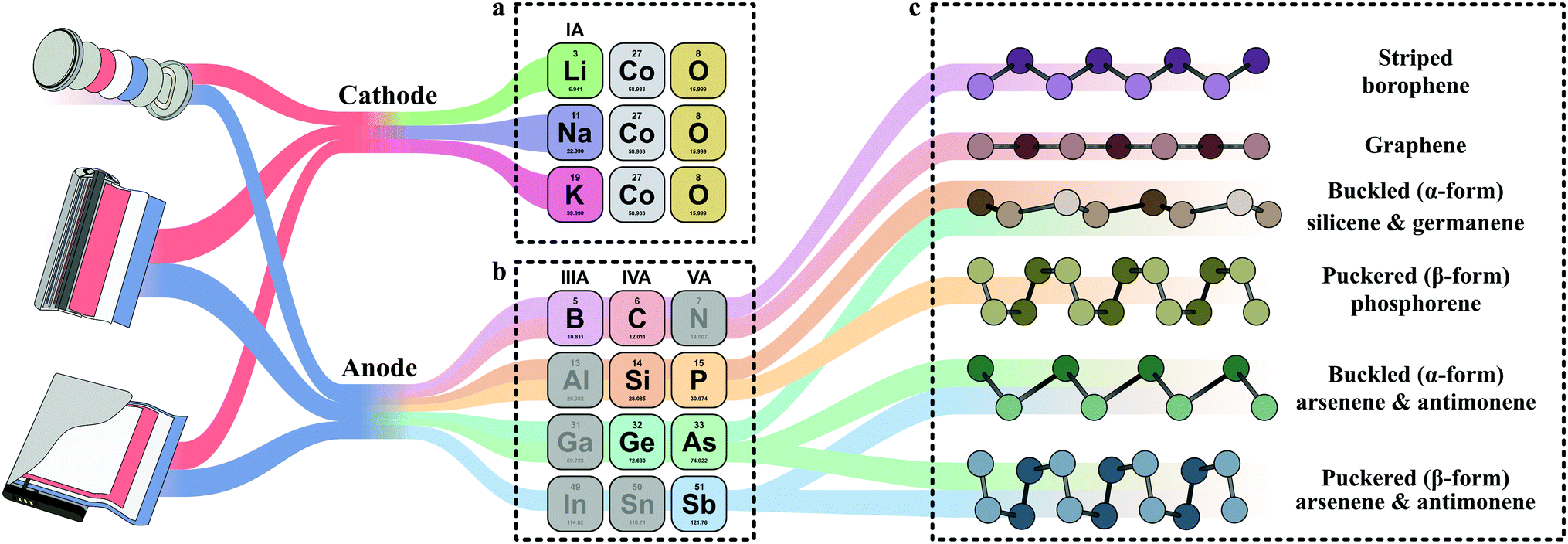 | ||
| Fig. 1 Typical material electrodes: (a) cathode alkali metal-ion batteries, i.e., LiCoO2, NaCoO2,93 and KxCoO2,94 (b) 2D elemental anodes, and (c) layered morphologies of 2D elemental layered materials and their common forms.95 | ||
2.5 Arsenene
Arsenene is comprised of a monolayer of arsenic and has a buckled hexagonal structure akin to elemental 2D materials from group IVA.62,96 If the bulk material is orthorhombic As, then the corresponding monolayer (α-As) is similar to phosphorene and exhibits a hexagonal structure.97 On the other hand, if the gray As is the initial material, then the monolayer exhibits a buckled structure and is termed β-As.97,98 With a predicted Young's modulus of 12.7 GPa, arsenene presents mechanical flexibility and highly anisotropic mechanical properties.99 In addition, arsenene has a semiconducting band structure with an indirect bandgap value of 2.49 eV and high carrier mobility.96,100 Mechanical strain, such as strain-induced band transition, modulates the electronic properties in this elemental monolayer species. According to Kong et al., 12% biaxial tensile strain on doped arsenene (at a temperature of 30.8 K) makes arsenene superconducting.101 Although most arsenene research has relied on theoretical calculations or first-principles calculations, fabrication of arsenene monolayers and experimental confirmation of theoretical predictions are emerging.1022.6 Antimonene
Antimonene, a monolayer of antimony (Sb) metal, exists in several allotropic forms. The most stable form is rhombohedral beta-phase antimonene, which has a buckled hexagonal structure with promising thermal and electronic properties. The indirect band gap of the β-antimonene form is predicted to be 1.2 eV,103,104 whereas the band gap is direct and predicted to be smaller in the α-antimonene form.104 From the visible region to ultraviolet region, antimonene shows exceptional light absorbance for optical properties.1042.7 Borophene
Borophene is a single layer of synthesized boron atoms that exists in different phases, e.g., rectangular and rhombohedral phases.105 Typically, four phases have been observed: 2-Pmmn, β12, χ3, and honeycomb.65 Borophene has highly anisotropic electronic properties and mechanical properties, meaning that a characteristic metallic band structure is evident along the armchair direction (with fast ion-transport characteristics) and a large band gap is present along the zigzag orientation in hexagonal borophene.65,106 Theoretical calculations suggest that the Young's modulus along the armchair orientation is ∼398 N m−1, which is higher than that of graphene, and approximately 180 N m−1 along the zigzag direction.1063. Synthesis and characterization of elemental 2D nanomaterials
Synthesis of elemental 2D nanomaterials significantly impacts their physiochemical and electronic properties. The synthesis of elemental nanosheets was inspired by the fabrication of 2D graphene from bulk graphite via mechanical exfoliation in 2004.107 Because of its attractive properties and diverse implementations, numerous fabrication methods, such as bottom-up growth to top-down exfoliation processes, have been used to produce graphene.70,73,107–113 Based on the fabrication process of graphene, other elemental 2D nanomaterials have been synthesized, including silicene,114 germanene,115 stanene,51 phosphorene,87 arsenene,116 antimonene,117 bismuthine,118 borophene,106 and gallenene.119 This section introduces fabrication and characterization methods commonly used to produce single-elemental 2D nanomaterials for electrochemical applications. The synthesis techniques, as shown in Fig. 2, can generally be classified as (a) top-down (e.g., mechanical exfoliation [cleavage], liquid exfoliation [ultrasonication], and etching) and (b) bottom-up (e.g., chemical and physical vapor deposition and wet chemical solvothermal reaction).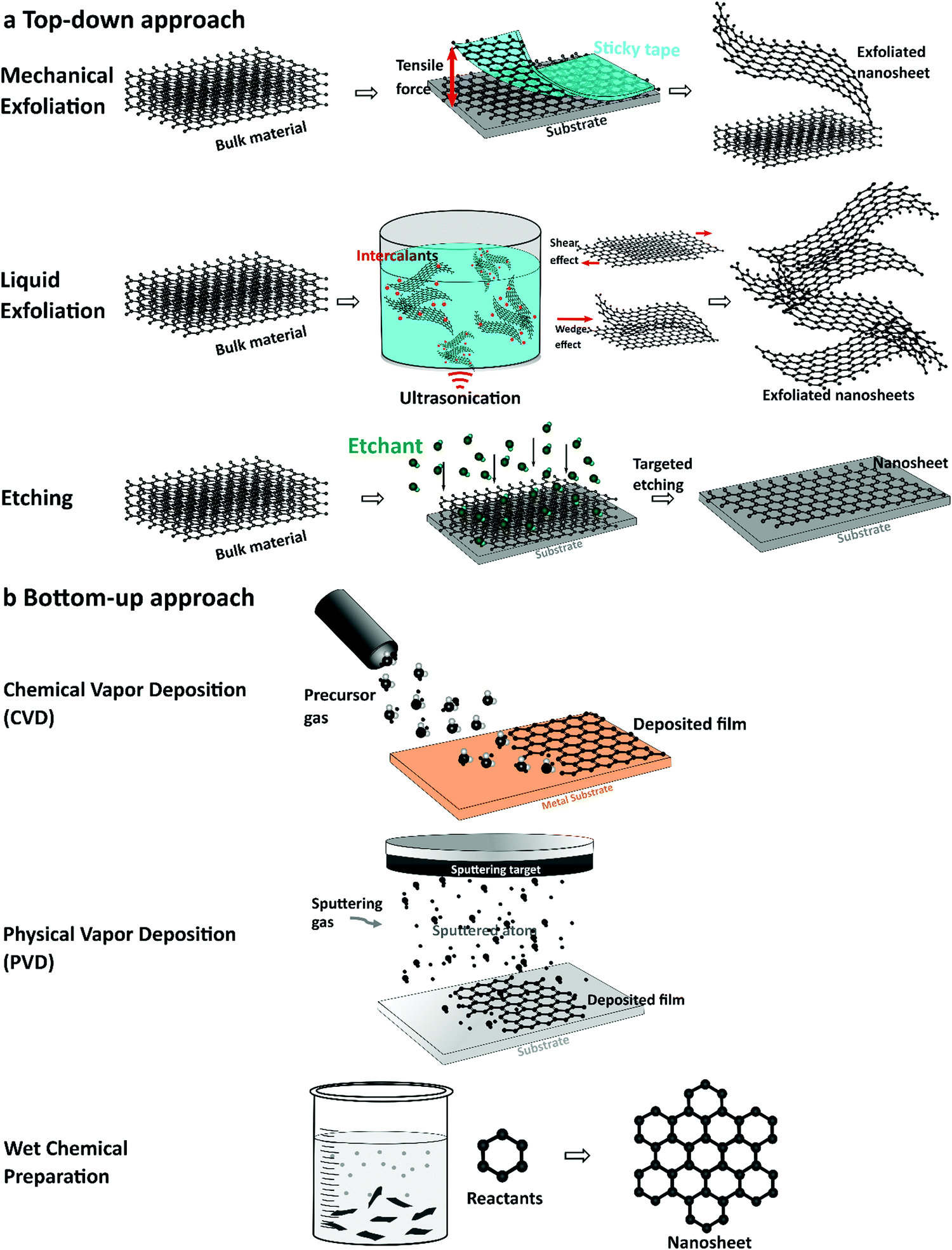 | ||
| Fig. 2 Schematic illustration of the general synthesis techniques of elemental 2D elements. (a) Top-down approaches. (b) Bottom-up approaches. | ||
3.1 Graphene
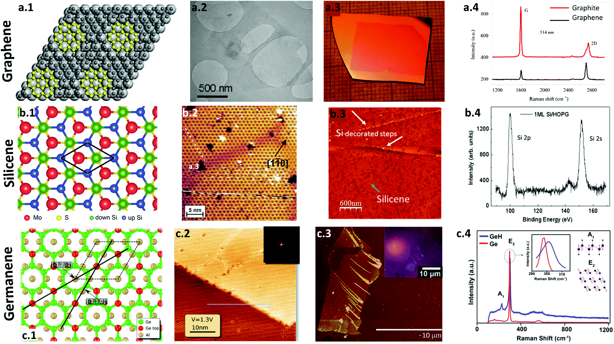 | ||
| Fig. 3 Synthesis and characterization of graphene, silicene and germanene. (a) Graphene. (a.1) A schematic of a defect free graphene synthesis via CVD at approximately 150 °C using Ti (∼10 nm)-coated substrates. Reproduced with permission.123 Copyright 2018, American Chemical Society. (a.2) TEM image of a monolayer graphene flake synthesized by liquid exfoliation. Reproduced with permission.124 Copyright 2009, American Chemical Society. (a.3) Photograph of PMMA derived graphene on a SiO2/Si substrate grown at 1000 °C. Reproduced with permission.125 Copyright 2011, American Chemical Society. (a.4) Raman spectra of graphite and monolayer graphene show a sharp 2D peak for graphene with an FWHM of 30 cm−1. Reproduced with permission.122 Copyright 2013, National Academy of Sciences of Armenia. (b) Silicene. (b.1) Schematic representation of a buckled silicene grown on a MoS2 substrate. Reproduced with permission.126 Copyright 2014, American Chemical Society. (b.2) An STM image of a 2D Si layer reveals a honeycomb-like structure. The dark centers are separated by 1.14 nm, which corresponds to (4 × 4) symmetry. Reprinted figure with permission from ref. 114. Copyright 2012 by the American Physical Society. (b.3) AFM image of a monolayer silicene deposited on highly oriented pyrolytic graphite (HOPG) at room temperature. The silicene thin films are indicated by a light blue arrow, where the HOPG substrate are the darkest regions, with the small 3D Si clusters (1 nm height) indicated by white arrows. (b.4) An XPS spectrum of silicene shows the distinct peaks of Si 2p and Si 2s obtained after deposition. Reproduced with permission.127 Copyright 2016, American Chemical Society. (c) Germanene. (c.1) Schematic representation of a germanene monolayer on an Al substrate. (c.2) Large scale STM image of germanene on Al(111). The line indicates the direction of Al [−1 2 −1]. The hexagonal periodicity of the germanene lattice is shown in the inset using Fast Fourier transform (FFT). Reproduced with permission.128 Copyright 2015, American Chemical Society. (c.3) AFM micrograph of few-layer germanene deposited on SiO2/Si. (c.4) Raman spectra of hydrogen-terminated germanene GeH and Ge powder show the variations in the E2 peak. Reproduced with permission.115 Copyright 2013, American Chemical Society. | ||
Similarly, Lotya et al. utilized ultrasound to disperse graphite in a surfactant–water solution, resulting in a large amount of multilayer graphene (<5 layers) and a smaller amount of monolayer graphene.124 Transmission electron microscopy (TEM), Raman spectroscopy, infrared (IR) spectroscopic analysis, and X-ray photoelectron spectroscopy (XPS) of these films showed defect- and oxidation-free dispersed graphene flakes. The TEM image of graphene flakes in Fig. 3a.2 showed a monolayer graphene, and the Raman spectra showed that the small graphene flakes exhibited a low intensity in the D-band, while the big flakes showed no D-band, which suggests that the graphene flakes had low defect content. The XPS confirmed low levels of oxidation of the graphene film.
Liu et al. used expandable graphite (EG) to produce FLG in supercritical N,N-dimethylformamide (DMF) in less than 15 minutes, followed by exfoliation of FLG in supercritical DMF to produce monolayer graphene.131 AFM and Raman results indicated the presence of FLG (thickness ∼3 nm) and monolayer graphene (thickness ∼1.2 nm), but a small proportion of defects were present in the synthesized graphene sheets. Other researchers have also recently attempted to produce large-scale graphene sheets using liquid-phase exfoliation.132–135 Although liquid-phase exfoliation shows promise for synthesizing large-scale graphene, it suffers from impurity and the presence of oxygen, resulting in the poor electrical properties of graphene.
In another approach, Yu et al. produced high-quality graphene on polycrystalline Ni foils using surface segregation and substrate transfer.137 For synthesis, a CH4![[thin space (1/6-em)]](https://www.rsc.org/images/entities/char_2009.gif) :H2:Ar (0.15:1:2 ratio) precursor gas mixture was utilized at 1000 °C for 20 minutes. High-resolution TEM (HRTEM) showed 3–4 layers of graphene, which was confirmed by Raman spectroscopy. According to the authors, the cooling rate significantly affects the amount and quality of the carbon segregated at the surface of the Ni, and the quality of graphene films can be monitored by varying the surface roughness of the substrates and the flow rate of H2.
:H2:Ar (0.15:1:2 ratio) precursor gas mixture was utilized at 1000 °C for 20 minutes. High-resolution TEM (HRTEM) showed 3–4 layers of graphene, which was confirmed by Raman spectroscopy. According to the authors, the cooling rate significantly affects the amount and quality of the carbon segregated at the surface of the Ni, and the quality of graphene films can be monitored by varying the surface roughness of the substrates and the flow rate of H2.
Wang et al. synthesized large-scale, substrate-free graphene sheets.138 These FLG sheets were synthesized from CH4:Ar (1:4 v/v) over magnesium oxide-supported cobalt catalysts at 1000 °C. The FLG was first cleaned with concentrated HCl to wash off MgO and Co and then rinsed with distilled water to obtain a neutral pH. HRTEM showed randomly aggregated, thin, crumpled graphene sheets, and Raman spectra confirmed at least five layers in the graphene sample.
Sun et al. obtained a monolayer pristine graphene film from a thin film (∼100 nm) of spin-coated poly(methyl methacrylate) (PMMA).139 Cu metal was used as the catalyst substrate, and graphene was grown at a low temperature of 800 °C with a reductive gas flow (H2/Ar), resulting in monolayer graphene with a thickness of 0.7 nm as measured by AFM. The I2D/IG intensity ratio in the Raman spectra of this PMMA-derived graphene was approximately 4, with a full-width at half-maximum (FWHM) of 30 cm−1 for the 2D peak, proving that the produced graphene was a monolayer.
Park et al. used CVD to synthesize high-quality, defect-free, micrometer-scale graphene at a low temperature of 150 °C (Fig. 3a.1).123 First, they coated a glass substrate with a 10 nm Ti layer annealed under hydrogen; TEM and Raman spectroscopy confirmed defect-free graphene synthesis on the Ti-coated substrate. In a slightly different approach, Li et al. demonstrated a CVD technique using a solid and a liquid precursor to grow graphene at low temperatures.125 From solid PMMA and polystyrene precursors, monolayer graphene films were grown on Cu foils at a low temperature of 400 °C. High-quality monolayer graphene films were synthesized at a low growth temperature of 300 °C when liquid benzene was utilized as the hydrocarbon source. Macroscopic uniformity was achieved in PMMA-derived graphene grown at 1000 °C, as shown in Fig. 3a.3. SEM of graphene grown at 700 °C and 400 °C confirmed the continuity of graphene films grown at lower temperatures. Raman spectroscopy at 550 nm showed a noise-level D band, which confirmed the presence of monolayer graphene films on the SiO2/Si substrate.
Researchers in another study used CVD to synthesize large-scale, high-quality graphene from methanol, ethanol, and propanol precursors on copper foil.140 The Cu film was exposed to alcohol vapor for approximately 5 minutes, and the average growth temperature was 850 °C. The alcohol precursors yielded continuous monolayer sheets of graphene, and Raman spectra and XPS showed that the synthesized graphene sheets were of high quality and had no measurable doping or oxidation effect. The field-effect mobility was measured as 1800–2100 cm2 V−1 s−1 at carrier densities between 1011 cm−2 and 1012 cm−2 for large-area graphene transistors.
Some other studies involving syntheis of graphene are also noteworthy such as dechlorination of hexachlorobenzene on Cu foils;141 making low-cost graphene from organic matter such as food, insect, and waste;142 using solid coronene as a carbon precursor;143 two-step CVD;144 plasma-assisted CVD;145,146 direct synthesis of FLG on NaCl crystal;147 and template-directed CVD of graphene foams.148
3.2 Silicene
Because silicon is in the same group IV as graphite, advances in graphene have increased interest in silicene, a 2D hexagonal lattice derived from silicon. Silicene has a hexagonal surface pattern with a periodicity of 3.2 Å (Fig. 3b.1). In 2006, Nakano et al. used chemical exfoliation of CaSi2 to prepare silicon sheets. CaSi2 was first doped with Mg, followed by absorption of CaSi1.85Mg0.15 in a propylamine hydrochloride solution.149 The Ca+ ions were deintercalated with the evolution of hydrogen, and a light-brown suspension of silicon sheets was formed. AFM was used to measure the average thickness of the sheets (i.e., 0.37 nm), and TEM showed a 2D structure of silicon sheets with lateral dimensions of 200–500 nm. The synthesis of silicon sheets in this report expanded future silicene research.Vogt et al. utilized CVD for depositing silicene film on Ag(111) surfaces.114 The Ag surfaces were prepared by Ar bombardment (1.5 kV, 5 × 10⁻⁵ mbar) and then annealed at 530 °C for 30 minutes under ultra-high vacuum (UHV) conditions. Silicene was deposited on Ag by evaporating a piece of Si-wafer while maintaining the temperature of Ag substrate at 220–260 °C. The Si 2p-to-Ag 4d area ratio of XPS peaks indicated 2D growth of Si with the deposition, and the low-energy electron diffraction (LEED) pattern showed a 4 × 4 symmetry of a Si monolayer. The authors used scanning tunnelling microscopy (STM) and angle-resolved photoemission spectroscopy (ARPES) to confirm that the (4 × 4) 2D Si adlayer on Ag(111) was, in fact, a 2D silicene sheet with a honeycomb structure (Fig. 3b.2).
Tao et al. performed epitaxial silicene synthesis on an Ag(111) thin film on a mica substrate without using expensive single-crystal bulk Ag.79 Raman spectroscopy confirmed the formation of silicene on the Ag substrate with strong peaks in the range of 515–522 cm−1, which corresponded to E2g modes and symmetric stretching of silicon atoms.
Crescenzi et al. deposited silicon directly onto a graphite substrate at room temperature to demonstrate that using a highly oriented pyrolytic graphite (HOPG) substrate prevented the interaction between silicene and the substrate.127 The sp2 electronic configuration and fully honeycombed structure of the HOPG resulted in chemical inertness. AFM images of the silicene showed a clean, uniform surface (Fig. 3b.3), and XPS of the silicene confirmed that Si peaks were highly symmetrical and did not oxidize during the synthesis (Fig. 3b.4).
Okamoto et al. reported the synthesis of silicene with large lateral size (1–2 μm) and oxygen-free surfaces.150 They chemically exfoliated polysilane (Si6H6) with n-decylamine and dissolved the mixture in an organic solvent. The solvents were slowly evaporated under a nitrogen atmosphere to form a silicon sheet that was densely covered with n-decylamine residues. Results showed that amine precipitates were bound covalently to the Si(111) planes.
Several research groups have also developed surface segregation of silicene on ZrB2,151 buckled silicon on Ir(111),152 stabilization of silicene,153 freestanding silicon nanosheets (SiNSs) via hydrosilylation reactions,154 and magnesiothermically induced phase transition of exfoliated silicene nanosheets155 to successfully synthesize silicene.
3.3 Germanene
Because of its location in the periodic table of elements in the same group of carbon and silicon, germanene has also become a topic of interest in atomically thin 2D materials research. In 2013, Bianco et al. performed the first synthesis of a graphene analogue of germanium, millimeter-scale hydrogen-terminated germanium (germanane, GeH).115 This hydrogenated germanene was produced from CaGe2 using topochemical deintercalation. The GeH was shown to be thermally stable up to 75 °C, and XPS and FTIR confirmed that the surface layer of GeH slowly oxidized in air over 5 months. An AFM micrograph showed mechanically exfoliated GeH sheets as single- and few-layered on SiO2/Si surfaces with lateral sizes greater than 2 μm (Fig. 3c.3). Raman spectroscopy showed a shift in the E2 peak between hydrogen-terminated germanene and germanium, as shown in Fig. 3c.4.Li et al. produced a buckled germanene sheet on a Pt(111) surface.156 After depositing germanium on Pt from a germanium rod mounted in an electron beam evaporator, the sample was annealed at a temperature of 600–750 K for 30 minutes. According to the authors, annealing the sample at temperatures below 800 K prevented the formation of a Ge–Pt surface alloy. LEED was used to macroscopically specify the structure as a (√19 × √19) superstructure, and STM showed the lattice constant of the structure to be 12 Å. Similarly, Derivaz et al. fabricated a continuous germanene layer on an Al(111) surface.128 The germanene layer was characterized by a (3 × 3) superstructure with respect to the substrate (Fig. 3c.1), and a large-scale STM image of Al(111) showed the long-range structure of germanene (Fig. 3c.2). The thickness of the synthesized germanene was approximately 0.27 ± 0.01 nm.
Davila et al. produced atomically thin, ordered 2D germanene sheets using molecular beam epitaxy (MBE) on an Au(111) substrate.85 Zhang et al. showed the growth of buckled germanene on a non-metallic MoS2 surface.157 Germanene's lattice constant was 20% larger than the lattice constant of MoS2 with an angle of 0° between them.
3.4 Phosphorene
Phosphorene, which is primarily derived from black phosphorus, is an allotrope of phosphorus, a group V element. Phosphorus has white, red, black, blue, and violet phosphorus allotropes. Black phosphorus has a 2D morphology, making it a promising material for synthesizing phosphorene. In 2014, Liu et al. introduced phosphorene using mechanical exfoliation of layered bulk black phosphorus.87 Exfoliated phosphorene was transferred onto a SiO2/Si substrate and then cleaned with alcohol and heated at 180 °C to remove the residue. AFM showed the thickness of the monolayer phosphorene to be 0.85 nm. During the same period, Buscema et al. and Li et al. used Scotch tape-based mechanical exfoliation to fabricate a few layers of phosphorene from a bulk crystal of black phosphorus.90,158Lu et al. demonstrated Ar+ plasma thinning and mechanical cleavage to synthesize monolayer phosphorene.159 AFM and contrast spectra determined the sample thickness, and the measured heights were 0.85 nm and 2.8 nm, respectively, which were consistent with the monolayer and pentalayer phosphorene. Raman frequency analysis showed an increase in the intensity ratio of A2g to A1g modes, which corresponded to the decrease in the thickness of bulk crystal to monolayer phosphorene.
Zhang et al. reported an MBE growth of monolayer blue phosphorus on Au(111) from black phosphorus.89 Black phosphorus was deposited by evaporation at 260 °C and annealed at 250 °C for 60 minutes. STM showed a well-defined monolayer phosphorus with a hexagonal appearance, and the simulated STM image created by DFT with a (4 × 4) supercell of blue phosphorus was in good agreement with the experimental STM image.
Castellanos-Gomez et al. proposed a modified version of the mechanical exfoliation technique to optimize the deposition of phosphorene on the substrate.160 Blue Nitto tape was used to cleave bulk black phosphorus, and the tape containing the thin flakes was pressed against a poly-dimethylsiloxane (PDMS) substrate. The PDMS substrate was then pressed gently onto a Si substrate to transfer the thin flakes to the Si. Use of an intermediate substrate increased the yield of the phosphorene and decreased the contamination. A TEM image confirmed the formation of a few layers of phosphorene after exfoliation, and TEM and Raman spectra of the flakes indicated that few-layer phosphorene flakes were highly crystalline and stable, even in freestanding form.
Kang et al. used liquid exfoliation to fabricate phosphorene.161 Black phosphorus was dispersed in NMP in a sealed-tip ultrasonication system to exfoliate in an anhydrous, oxygen-free environment. An AFM height image showed that the thicknesses of the single- to few-layer nanosheets were between 16 and 128 nm. XPS spectra confirmed the high chemical quality of the exfoliated black phosphorus nanosheets with partially oxidized POx peaks.
Similarly, Woomer et al. synthesized crystalline monolayer and few-layer phosphorene via liquid exfoliation from black phosphorus crystals.162 A SEM image confirmed the presence of phosphorene flakes with lateral sizes between 50 μm and 50 nm (Fig. 4a.2), and a TEM image revealed the thin, uniform morphology of the phosphorene flakes (Fig. 4a.3). XPS analysis also confirmed the defect-free phosphorene layers without oxidation (Fig. 4a.4). This study demonstrated a simple, scalable technique to synthesize high-quality phosphorene. Several liquid exfoliations161,163,164 and mechanical exfoliations165,166 have been reported over the last decade to successfully fabricate phosphorene nanosheets.
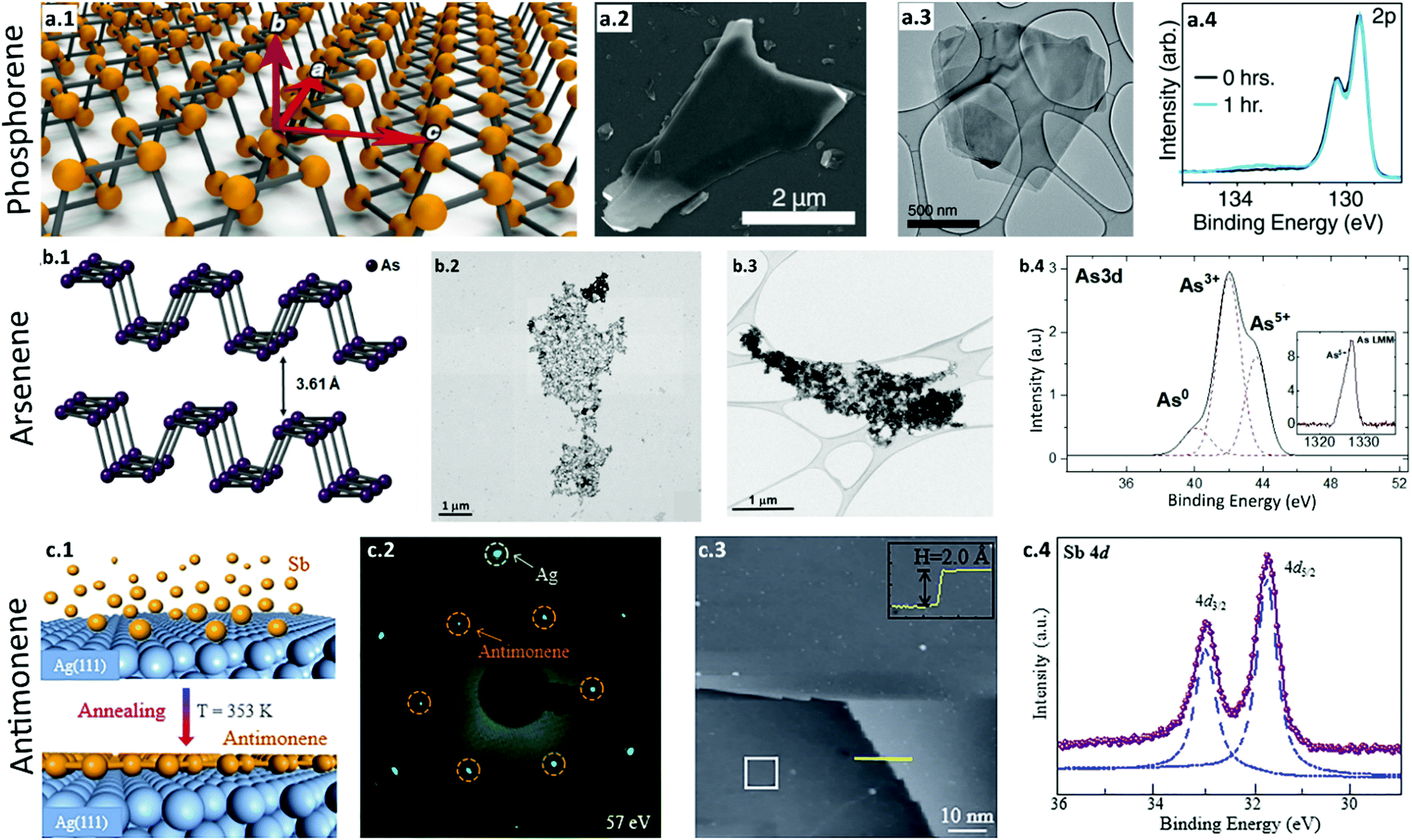 | ||
| Fig. 4 Synthesis and characterization of phosphorene, arsenene, and antimonene. (a) Phosphorene. (a.1) Schematic illustration of a phosphorene monolayer showing the conventional zigzag (a) and armchair directions (c). (a.2) SEM image of liquid-exfoliated thin phosphorene flakes. (a.3) TEM images of few-layer phosphorene. (a.4) XPS analysis of unoxidized few-layer phosphorene sheets (black). When the sheets are exposed to light (λ = 460 nm) and oxygen, they become oxidized (blue). Reproduced with permission.162 Copyright 2015, American Chemical Society. (b) Arsenene. (b.1) Schematic illustration of monolayer arsenene with an orthorhombic structure. (b.2) STEM image of the electrochemically exfoliated ultrathin flakes of few-layer arsenene. (b.3) High-resolution TEM image of the arsenene nanosheets. (b.4) XPS spectra of arsenene with peaks corresponding to elemental arsenic. Reproduced with permission.167 Copyright 2020, American Chemical Society. (c) Antimonene. (c.1) Schematic of the fabrication process of high-quality monolayer antimonene. Antimony atoms are deposited onto an Ag(111) substrate which is kept at 353 K. (c.2) LEED pattern of antimonene on the Ag substrate. Hexagonal diffraction patterns present a √3 × √3 superstructure with respect to the Ag(111) substrate. (c.3) A large scale STM image demonstrates a homogenous thin film of single-layer antimonene with a height of 2.2 Å. (c.4) XPS spectra of SB 4d with two sharp peaks assigned to Sb in antimonene, which confirms the monolayer antimonene formation. Reproduced with permission.168 Copyright 2018, American Chemical Society. | ||
3.5 Arsenene
Arsenene is a layered 2D structure of another group V element, arsenic. In 2016, Tsai et al. studied a plasma-assisted route to prepare multilayer arsenene on an InAs substrate.169 The thickness of multilayer arsenene was controlled by adjusting the annealing time, power, and exposure time of plasma. According to the authors, the optimized synthesis conditions were N2 plasma immersion with 100 W power for 30 minutes and annealing at 450 °C for another 30 minutes. The heterogenous structures of arsenene, InN, and the InAs substrate were visible by TEM, and the TEM-measured interlayer distances of 0.286 nm and 0.181 nm corresponded to the (110) and (01−1) interplanar distances, respectively, of the multilayer arsenene. In 3d and As 3d, XPS spectra revealed that the InN formed during annealing pushed the arsenic atoms to the outer surface to form layers of arsenene, which was identified at ∼42.4 eV.Gusmao et al. showed that aqueous shear exfoliation could produce arsenene nanosheets.116 Kitchen blenders were used to disperse and exfoliate bulk As crystals in aqueous surfactant sodium cholate (1 g L−1, SC 5 g L−1) for 2 hours. SEM images of exfoliated arsenene showed heterogenous sub-micron nanosheets, and a TEM image revealed anisotropic arsenene sheets with a visible wrinkled structure consisting of a few layers.
Recently, Kovalska et al. exfoliated arsenic electrochemically to synthesize arsenene.167 Orthorhombic arsenic (Fig. 4b.1) was exfoliated in a 0.01 M NH4PF6/DMF solution. STEM (Fig. 4b.2) and low-magnification, bright-field TEM (Fig. 4b.3) images of sonicated arsenene showed netlike, agglomerated arsenene flakes, and XPS spectra (Fig. 4b.4) of the electrochemically exfoliated arsenene showed peaks that corresponded to elemental arsenic. This nonaqueous oxygen-free medium facilitates the synthesis of high-quality, few-layer arsenene.
Vishnoi et al. exfoliated grey arsenic in NMP to produce few-layer arsenene under a nitrogen atmosphere.100 A low-magnification TEM image and the corresponding selected area electron diffraction (SAED) pattern of few-layer arsenene showed the hexagonal lattice of rhombohedral As. Raman spectra of few-layer arsenene showed peaks at 197.2 and 256.5 cm−1, which corresponded to the Eg and A1g vibrational modes of the β-arsenene.
3.6 Antimonene
Antimonene is an exfoliated monolayer structure of group V material antimony. Antimony has several allotropes, of which grey antimony is the most stable and is primarily used to fabricate antimonene. Ji et al. showed van der Waals epitaxy growth of few-layer antimonene on a fluorophlogopite mica substrate.117 Antimony powder was evaporated at 660 °C, deposited on the mica substrate kept at 380 °C, and then cooled to room temperature. An AFM image of the antimonene sheet showed a thickness of 4 nm, and Raman spectroscopy revealed a buckled hexagonal structure consistent with the monolayer β-phase antimonene.Tsai et al. used a plasma-assisted approach to produce multilayer antimonene on an InSb substrate.170 The InSb substrate was first immersed in N2 plasma to form antimonene layers at 100 W for 30 minutes and then annealed at 450 °C for 30 minutes. Raman spectra of the synthesized antimonene indicated the formation of thin films.
Shao et al. reported an epitaxial growth of monolayer antimonene with a honeycomb structure on an Ag(111) surface (Fig. 4c.1).168 The LEED pattern of antimonene in Fig. 4c.2 showed a defect- and wrinkle-free pristine hexagonal structure. A large-scale STM image showed synthesis of high-quality monolayer antimonene (Fig. 4c.3), and the XPS spectra in Fig. 4c.4 showed two distinct Sb peaks, confirming the formation of an antimonene monolayer. This high-quality flat antimonene monolayer is an excellent candidate for application in future electronics.
Ares et al. demonstrated micromechanical exfoliation of antimony to produce single- and few-layer antimonene flakes.61 They used an intermediate viscoelastic surface to increase the yield and reduce the defects, and then they transferred the antimonene flakes onto a SiO2/Si substrate. A single-layer antimonene with a thickness of 0.9 nm was observed using AFM, and high-resolution TEM was used to distinguish thick flakes from the bulk and antimonene flakes confirmed the hexagonal lattice of β-antimonene.
Gibaja et al. utilized rapid liquid-phase exfoliation to produce highly stable, few-layer antimonene.171 Bulk antimony was dispersed in an isopropanol:water (4:1 ratio) mixture without any surfactant to produce micrometer-large antimonene. The exfoliated few-layer antimonene sheets were stable under ambient conditions for long periods of time (e.g., weeks). AFM confirmed the fabrication of few-layer antimonene, and Raman spectra showed that the layer thickness of ∼4 nm corresponded to a monolayer or bilayer of antimony.
3.7 Borophene
Borophene, which consists of the 2D forms of elemental boron, is an element in group III of the periodic table of elements and has been successfully synthesized in experiments. Depending on the bonding between boron atoms, 16 unique allotropes of bulk boron can be formed.172 Although these allotropes show various structures, borophene refers to the general class of 2D boron sheets.In 2015, Mannix et al. used an electron beam evaporator to grow borophene sheets under UHV on an Ag(111) substrate while maintaining a temperature of 450–750 °C.106In situ Auger electron spectroscopy (AES) revealed a boron KLL peak in the clean Ag(111) spectrum, confirming the formation of boron nanosheets. STM and XPS results confirmed the metallic characteristics of borophene and proved that bulk boron allotropes are semi-conductors under standard conditions. Annular bright-field (ABF) images showed sheet thicknesses of 0.27–0.31 nm, which corresponded to the monolayer structure of boron nanosheets.
Feng et al. presented a similar experimental study using MBE to synthesize borophene nanosheets on an Ag(111) surface under UHV.173 They showed that the deposited borophene on the Ag substrate had monolayer structures. STM images revealed that two types of boron sheets were formed, a β12 sheet and a χ3 sheet, at substrate temperatures of 570 K and 680 K, respectively. Both showed buckled triangular lattices but different hexagonal holes in the structure. XPS study confirmed that the sheets were inert to oxidation and interacted only with the Ag substrate. Recently, Kiraly et al. reported the growth of borophene on Au(111) substrates using the MBE method.174 UHV STM showed the herringbone reconstruction to a trigonal network of nanoscale borophene islands (Fig. 5a). Boron was diffused into Au at a high temperature of 550 °C, followed by segregation to the surface when the substrate was cooled (Fig. 5b). The magnified image of the borophene islands revealed the atomically thin borophene with a strong periodicity of ∼0.66 nm, as shown in Fig. 5c and d.
 | ||
| Fig. 5 Synthesis and characterization of borophene. (a) STM images of boron deposition on clean Au(111) at 550 °C. The conventional herringbone reconstruction changes to a trigonal network, where nanoscale borophene islands emerge at the nodes, resulting in templated growth across the surface (highlighted by a white dashed line). (b) A schematic illustration of borophene growth shows that the boron forms a cluster on the surface at low substrate temperatures. At a higher temperature of 550 °C, the boron dissolves into the bulk and then separates to the surface to build up 2D borophene sheets upon cooling. (c) An STM image of a larger borophene island shows the herringbone reconstruction (black arrows) from the Au(111) substrate (V = 1 V, I = 100 pA). (d) Atomic-scale periodicity in larger borophene sheets (V = −0.4 V, I = 80 pA). (e) FFT of the STM image in (d) shows a strong periodicity of ∼0.66 nm in the extended borophene sheets. Reproduced with permission.174 Copyright 2019, American Chemical Society. | ||
Tai et al. used the CVD method to synthesize atomically thin γ-boron films on a Cu substrate.175 A mixture of boron and B2O3 powder was heated to 1100 °C and carried by H2 gas on 25 μm Cu foil. An AFM image showed that the thickness of the deposited film was 0.80 nm, indicating the formation of a monolayer. HRTEM images confirmed that the monolayer lattice structure corresponded to the orthorhombic γ-B23 crystal structure.
Ji et al. used a unique top-down process to synthesize high-quality ultra-thin boron nanosheets by combining liquid-exfoliation and thermal oxidation etching techniques.176 Highly dispersed boron sheets were prepared by exfoliating bulk boron in NMP (ethanol (1:1 v/v) solution) and then oxidizing it at 650 °C in air to form B2O3. This oxidized B2O3 was then dissolved into water to form BO33− with a second liquid exfoliation. Consequently, bulk boron decreased to ultra-thin boron nanosheets with an average size of 110 nm and an average thickness of 3 nm. HRTEM and high-resolution XPS confirmed the formation and crystalline nature of the boron nanosheets.
4. Electrochemical properties
The outstanding physical, chemical, electronic and optical properties of elemental 2D nanomaterials have led to numerous applications. These ultrathin nanomaterials have been explored in the areas of novel electronics and optoelectronics, energy storage and conversion, catalysts, water treatments, etc. This section will specifically summarize the recent progress in the utilization of elemental 2D nanomaterials as electrodes in electrochemical energy storage devices (e.g. supercapacitors and rechargeable batteries).4.1 Supercapacitors (SCs)
Supercapacitors have emerged as promising energy storage devices because of their high power density, high rate capability, excellent cyclability, low cost, and stable operating conditions.177 Supercapacitor materials store charges through electrostatic ion adsorption on their surfaces and these types of supercapacitors are known as electrical double-layer capacitors (EDLCs). Aside from EDLCs, some supercapacitor materials known as pseudocapacitors (PCs) can store charges created on the faradaic reactions on the surface of the electrode. Elemental 2D nanomaterials with only a few-layer thickness have readily available high surface areas and short diffusion paths for electrolyte ions. Thus, they have received increasing attention as promising electrodes to achieve high-performance supercapacitors.Graphene has been widely explored as a supercapacitor electrode owing to its highly tunable surface area (up to 2675 m2 g−1), high electrical conductivity, and theoretical capacitance (550 F g−1).25 However, graphene layers tend to agglomerate during preparation and application, which leads to low surface area and thus results in poor capacitance. As a result, several routes have been developed by researchers to avoid the cluster of the graphene layers and achieve high capacitance. For example, Stoller et al. pioneered a chemically modified graphene (CMG) which had a surface area of 705 m2 g−1 and an electrical conductivity of ∼2 × 10² S m−1.113 This CMG material delivered 135 and 99 F g−1 in aqueous (5.5 M KOH) and organic (1 M TEA BF4 in acetonitrile) electrolytes, respectively. This study showed that the graphene material worked well with commercial electrolytes and its good electrical conductivity contributed to low equivalent series resistance (ESR). Yu et al. incorporated 1D carbon nanotubes (CNTs) to physically separate 2D graphene nanosheets.178 Polymer-modified graphene sheets were homogenously dispersed, and the resultant sheets were assembled sequentially with CNTs. The obtained hybrid films demonstrated a gravimetric capacitance of 120 F g−1 even at a high scan rate of 1 V s−1, resulting from their well-defined nanoporous structure. In another approach, three-dimensional (3D) mesoporous carbon spheres inserted between the layers of graphene sheets were used as supercapacitors by Lei et al.179 The mesoporous structure reduced the ion diffusion resistance and improved the electronic conductivity, which resulted in a high-rate capability of the supercapacitor. This electrode also showed a capacity retention of ∼94% after 1000 galvanostatic charge–discharge cycles. Xu et al. reported a hierarchical porous structure of a 3D holey graphene framework (HGF) as a high-performance free standing electrode for supercapacitors.180 This holey framework allowed high surface area (830 m2 g−1), high electron and ion transport, and high packing density. The as-prepared HGF delivered a high specific capacitance of 298 F g−1 and volumetric capacitance of 212 F cm−3 at 1 A g−1 in 1-ethyl-3-methylimidazolium tetrafluoroborate/acetonitrile (EMIMBF4/AN) electrolyte. Besides, some other methods have been proposed in recent years to separate graphene sheets with nanomaterials181–186 and fabricate porous graphene frameworks187–194 to develop graphene-based high-performance supercapacitors.
Among other group IV elemental 2D materials, silicene has been investigated using density functional theory (DFT).195,196 With the first-principles theory, it was shown that the quantum capacitance of silicene was larger than that of graphene due to the lower Fermi velocity near the Dirac point. Furthermore, the introduction of defects with doping could be utilized to increase the quantum capacitance. This result will stimulate further experimental work on silicene-based electrodes for supercapacitors.
Phosphorene is the most experimentally studied supercapacitor material from group V. One of the first studies on phosphorene as a supercapacitor electrode was reported by Hao et al.197 The authors liquid-exfoliated black-phosphorus (BP) nanoflakes and used them as an electrode in polyvinyl alcohol/H3PO4 (PVA/H3PO4) electrolyte. The as-prepared electrode delivered a volumetric capacity of 17.78 F cm−3 at a scan rate of 0.005 V s−1. The charge/discharge curves showed superior EDLC behaviour of BP nanoflakes and 15.5% capacitance loss after 10000 cycles. Xiao et al. reported high-energy micro-supercapacitors (MSCs) where the electrode was fabricated by depositing phosphorene and graphene nanosheets (PG-MSCs) layer-by-layer.198 The TEM images in Fig. 6a–c exhibit a uniform morphology of phosphorene nanosheets with interlayer spacings of 0.33 and 0.44 nm. The cross-sectional SEM image in Fig. 6d confirmed the uniform incorporation of phosphorene into the graphene nanosheets. The resultant electrode showed outstanding conductivity (319 S cm−1) and energy density (11.6 mW h cm−3). The PG-MSCs delivered a high areal capacitance and volumetric capacitance of ∼9.8 mF cm−2 and 37.5 F cm−3, respectively, at a scan rate of 5 mV s−1 as shown in Fig. 6(f–h). Recently, Zu et al. used phosphorene as a cathode in supercapacitors and showed a discharge capacitance of 3181.5 F g−1 at a current density of 0.25 A g−1 in 1 M H2SO4 and 0.5 M KI electrolyte.199 The capacitance retention was nearly 100% after 1000 charge/discharge cycles.
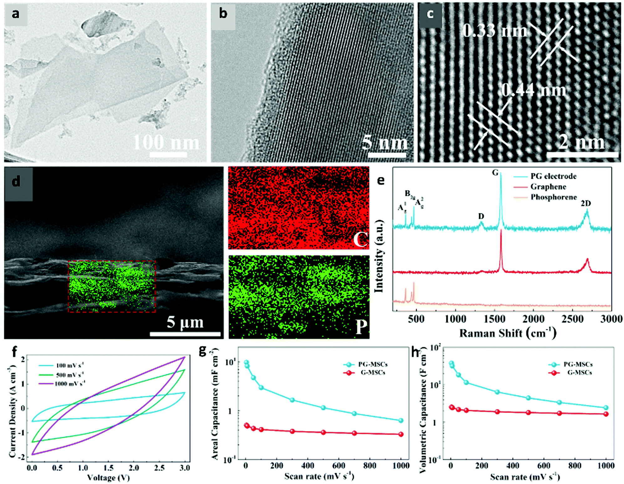 | ||
| Fig. 6 Structural and electrochemical characterization of phosphorene-graphene nanosheets (PG-MSCs) as a supercapacitor. (a) TEM and (b and c) HRTEM images of phosphorene exhibit a uniform morphology and crystal lattice. The interlayer distances of 0.33 and 0.44 nm confirm the high-quality of exfoliated phosphorene. (d) A cross-sectional SEM image shows that small phosphorene nanosheets are uniformly distributed into large graphene sheets. (e) A Raman spectrum of the PG film reveals the crystalline nature of phosphorene and graphene. (f) CV curves of PG-MSCs at different scan rates of 100–1000 mV s−1. (g) Areal capacitances and (h) volumetric capacitances of PG-MSCs and G-MSCs at different scan rates show the superiority of the layer-structured PG film for MSCs over planar MSCs (G-MSCs). Reproduced with permission.198 Copyright 2017, American Chemical Society. | ||
Antimonene was reported as an electrode material of a supercapacitor by Martínez-Periñán et al.200 Antimonene demonstrated a high capacitance of 1578 F g−1 at a high current density of 14 A g−1 in 0.5 M H2SO4. According to the authors, the high value of the capacitance was the result of both EDLC and faradaic reactions.
Among the other elemental 2D materials, borophene was reported to be used as an electrode material in supercapacitors. Li et al. demonstrated that few-layer boron sheets produced via liquid-phase exfoliation showed promising performance as supercapacitor electrode materials.201 The DMF-exfoliated boron sheets showed a specific capacitance of 147.6 F g−1 at a current density of 0.3 A g−1 in 1-butyl-3-methylimidazolium hexafluorophosphate as the electrolyte and 88.7% capacitance retention after 6000 cycles. The high specific capacitance and good rate capability of the as-prepared supercapacitor were attributed to the excellent electronic conductivity and layer structure of the B sheets, which offered abundant active sites and fast access to electrolyte ions.
In general, only a limited number of elemental materials were reported as supercapacitor electrodes. The agglomeration of layers after exfoliation and instability in the atmosphere lower the number of active sites and electronic conductivity of the elemental materials, leading to the poor performance of the supercapacitors. Thus, future studies are required to improve the architectures of the materials to enable efficient charge intercalation and deintercalation.
4.2 Rechargeable batteries
In order to improve the performance of future electronics and devices, rechargeable batteries must have improved storage capacities. Besides, to adopt the advances in small, wearable, flexible electronics, future energy storage devices must be light-weight and have high energy density. In this regard, elemental 2D materials are being considered as electrode materials in energy storage systems due to their large surface areas and form factors.4.2.1.1 Lithium-ion batteries (LIBs). Graphite is widely used as an anode material in LIBs owing to its low voltage range and reasonable specific capacity (372 mA h g−1) corresponding to the formation of graphite intercalation compounds (LIC6).202 However, to improve the reversible capacity and stability of LIBs, new electrode materials need to be developed. A graphene-based anode is considered to be a potential alternative as an anode in LIBs, because of its high specific surface area and superior electronic conductivity.107,203 Li+ ions can intercalate on each side of the graphene sheet, forming Li2C6, and hence can provide a maximum theoretical capacity of 740 mA h g−1.204
Large quantities of graphene nanosheets synthesized using chemical exfoliation were reported as anodes in LIBs by Wang et al. in 2009.205 The graphene nanosheets were evaluated in the potential range of 0.02 to 3.0 V at 1C rate and delivered a reversible capacity of 650 mA h g−1 in the initial cycle. The larger part of the specific capacity (>70%) was below 0.5 V, which was attributed to the lithium binding on the basal plane of the graphene nanosheets. The graphene anode showed a specific capacity of 460 mA h g−1 after 100 cycles, exhibiting enhanced lithium storage compared to a graphite anode. Similarly, graphene nanosheets (GNSs) were synthesized from artificial graphite (AG) by a fast heating process and ultrasonic treatment by Guo et al.206 The SEM showed the entangled GNSs with a curled and corrugated morphology of graphene. From XRD, it was found that the (002) peak of the GNSs became weakened, resulting in reduced crystallite size, which corresponded to the formation of defects in the GNSs. This was further confirmed by FTIR, which supported the presence of oxygen-functional groups in the GNSs. The as-prepared GNSs exhibited a reversible capacity of 672 mA h g−1 at 0.2 mA cm−2, which was almost twice the capacity of the AG. The enhanced performance of the GNSs was attributed to the storage of Li+ ions on both sides of the nanosheets along with the presence of functional groups and nanopores.
Goh et al. introduced a graphene “eggshell” in LIBs.207 They filled the void of graphene foam with curved graphene sheets, which after etching produced a graphene eggshell in the graphene foam structure (GE@GF) as shown in Fig. 7a. TEM images (Fig. 7b and c) revealed thin graphene layers with a crystalline shell structure. Raman spectrum (Fig. 7d) analysis confirmed the presence of few-layer graphene in the hybrid GE@GF. The Li+ intercalation into GE@GF is presented by a schematic in Fig. 7e. The electrochemical performance of both the electrodes exhibited that the initial coulombic efficiency increased from 66.3% for GF to 77.5% for the GE@GF electrode. For the GE@GF electrode, the first cycle reversible capacity after 45 cycles changed from 328 mA h g−1 to 368 mA h g−1, which was attributed to the interfacial storage of Li+ on the hollow graphene shell. In situ Raman spectroscopy (Fig. 7f) showed the intercalation mechanism of Li+ into the Ge@GF electrode. The Raman spectra showed that the G-band gradually moved to a higher wave number from 3.0 to 0.005 V vs. Li/Li+, which indicated the doping of graphene by Li. The Li doping level reached its maximum level and disappeared at 0.14 V, which was the indication of the formation of intercalation compound LiC6. According to this study, morphology control of the graphene foam by filling it with graphene sheets could improve the initial coulombic efficiency of the unfilled graphene foam by 17%.
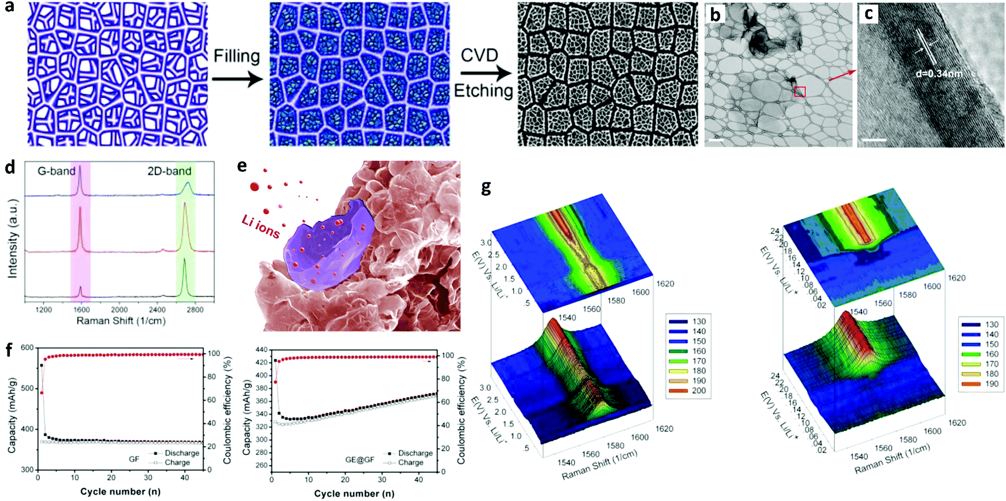 | ||
| Fig. 7 Structural characterization and electrochemical performance analysis of a graphene eggshell-filled graphene foam (GE@GF) as an anode in LIBs. (a) Schematic illustration of the graphene eggshell-filled graphene foam. (b) TEM image of the graphene eggshell structure (scale bar = 500 nm). (c) HRTEM image of the red square in part (b), showing a crystalline shell with an interlayer spacing of 0.34 nm (scale bar = 2 nm). (d) Raman spectroscopy shows two distinct peaks at ∼1580 cm−1 (G-band) and 2705 cm−1 (2D band). (e) Schematic illustration of Li+ intercalation into GE@GF. (f) Cycling performances of GE@GF and GF electrodes at a current density of 37 mA g−1. (g) In situ Raman spectra of the GE@GF electrode discharged from 3.0 to 0.005 V vs. Li/Li+ (left) with details ranging from 0.25 to 0.005 V vs. Li/Li+ (right). Reproduced with permission.207 Copyright 2014, American Chemical Society. | ||
Functionalizing or doping GNSs with nanomaterials is another approach to increase the storage capacity and stability of graphene-based electrodes in LIBs. Functional groups prevent the restacking of the GNSs and thus present a large surface area for the electrolyte immersion and adsorption on the electrode materials. For example, Wang et al. grew Mn3O4 on reduced graphene oxide (rGO) sheets for application in LIBs. The Mn3O4/rGO hybrid anode showed a high capacity of 900 mA h g−1 at 40 mA g−1.208 This performance was achieved due to the intimate interaction of the Mn3O4 nanoparticles with rGO sheets that made insulating Mn3O4 particles electrochemically active. A similar strategy was adopted by Zhou et al. where graphene was produced by in situ reduction of iron hydroxide between graphene nanosheets.209 The composite showed a high specific capacity of 1026 mA h g−1 at 35 mA g−1 after 30 cycles. The interleaved network of GNSs enhanced the electrical conductivity of the electrode as well as reduced the pulverization of the Fe3O4 particles. As a result, the GNS/Fe3O4 composite exhibited improved cycle stability and rate capability. The composite electrode exhibited 500 mA h g−1 at a current density of 700 mA g−1 after 100 cycles.
Besides, TiO2, Fe2O3, Co3O4, Li4Ti5O12, NiO, and NiCo2O4 have also been reported to make hybrid nanocomposites with graphene as advanced LIB anodes.210–215
Jiang et al. introduced monolayer MoS2 nanosheets with graphene aerogel to improve the electrochemical performance of LIBs.216 The structural and morphological compatibility of MoS2–graphene composite aerogels prevented the restacking and aggregation of MoS2 and graphene nanosheets and exhibited a high reversible capacity of 1200 mA h g−1 at 100 mA g−1. Layered-by-layered SnS2/graphene hybrid nanosheets were fabricated by Xia et al. to improve the conductivity of SnS2.217 Graphene acted as a buffer to suppress the volume change during the lithiation/de-lithiation of SnS2, leading to a high rate capability of 567.78 mA h g−1 at 2000 mA g−1.
4.2.1.2 Lithium–sulfur (Li–S) batteries. Because of their high theoretical capacity (1675 mA h g−1) and high energy density (2600 mA g−1), Li–S batteries are regarded as high energy rechargeable batteries. Li–S batteries utilize lithium as the anode and sulfur as the cathode. However, due to the large volume expansion and dissolution of lithium polysulfides, Li–S batteries show poor kinetics. Introducing graphene into sulfur can accommodate the volume expansion and also provide high surface area and capacity.218
Li et al. coated sulfur with rGO to confine the lithium polysulfides.219 When the polysulfide anions diffused into the electrolyte, the rGO coating restricted the sulfur and polysulfide anions in the carbon framework, and thus decreased the shuttling loss. As a result, a reversible capacity of 667 mA h g−1 at a high current density of 1.6 A g−1 after 200 cycles was achieved.
A graphene-coated mesoporous carbon/sulfur composite was introduced by Zhou et al.220 Mesoporous carbon acted as a buffer against the volume change of sulfur and provided an efficient diffusion path for Li+ ions during the charge/discharge process. The conductive rGO coating skin physically and chemically prevented the dissolution of polysulfides from the cathode as well as provided fast electron transport in the composite structure. The composite with 53 wt% sulfur exhibited a reversible discharge capacity of 734 mA h g−1 after 100 cycles at 0.5C.
Another approach is to introduce polymer into sulfur in addition to graphene. The polymer acts as a buffer against the volume expansion and graphene provides the electrical conducting path. Sulfur composited with curved graphene (CG) and coated with polyaniline (PANI) was reported as a composite cathode for Li–S batteries by Li et al.221 The composite (CG-S@PANI) electrode delivered a specific capacity of 1300 mA h g−1 at 33.44 mA g−1. The combination of graphene and the PANI coating provided an electronically conductive network that led to an improved cycling stability of the electrode.
In a different approach, Qiu et al. utilized nitrogen-doped graphene (NG) sheets as a matrix to wrap around sulfur particles.222 The highly conductive NG sheets with a large surface area exhibited significantly improved electronic conductivity. Besides, the self-generated curvature and wrinkles of the NG sheets facilitated electrolyte access throughout the structure and accommodated the volume change of S during charge/discharge. The Li/S@NG electrode delivered a high specific discharge capacity of ∼1167 mA h g−1 at 335 mA g−1 and showed an excellent coulombic efficiency of 97% after 2000 cycles.
Ding et al. tailored the structure of GNSs with KOH to create dense nanopores on the surfaces of the sheets.223 Sulfur was uniformly distributed and confined within the nanopores and maintained intimate contact with the tailored GNSs. The nanopores served as ‘micro-reactors’ for the electrochemical reactions, which suppressed the diffusion of polysulfides, leading to improved cycling stability. The resultant nanocomposites exhibited an initial reversible capacity of 1379 mA h g−1 at 0.2C and after 100 cycles the capacity retention was 74% at 1C.
4.2.1.3 Na-Ion batteries (SIBs). Similar to LIBs, graphene-based nanomaterials are promising electrode materials for energy storage in SIBs.224 A Na+ ion (1.02 Å) has a larger ionic radius than a Li+ ion (0.76 Å); thus, the electrode must possess large intercalation sites to allow diffusion of Na+ ions. Whereas graphite cannot accommodate Na+ ions, graphene can provide larger interlayer distances to store a larger number of Na+ ions.225,226
Wang et al. reported rGO as an anode in SIBs for the first time in 2013.225 The as synthesized rGO allowed significant Na+ ion insertion because of its large interlayer distances (∼0.371 nm) and disordered structures. The high magnification SEM image in Fig. 8a shows the layered, thin, and wrinkled structure of rGO. The HRTEM images in Fig. 8b and c confirmed the thin layers with larger interlayer spacings than graphite. The Raman spectrum in Fig. 8d further confirmed the presence of graphene sheets. The rGO anode showed a reversible capacity of 174.3 mA h g−1 at 40 mA g−1 after 250 cycles (Fig. 8e). Besides, rGO yielded a specific capacity of 141 mA h g−1 at 100 mA g−1 over 1000 cycles (Fig. 8f).
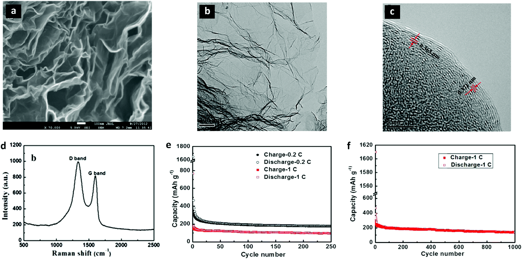 | ||
| Fig. 8 Structural characterization and electrochemical performance analysis of graphene sheets (rGO) as an anode in SIBs. (a) A high magnification SEM image (at 70 K) shows the rGO nanosheets with thin wrinkled structures of graphene layers. (b) A TEM image exhibits the transparent nanosheets, implying the presence of few layers with dark ripples of the sheets. (c) A high resolution TEM (HRTEM) image shows that the interlayer spacings of the (002) planes are 0.365–0.371 nm in different areas. (d) The Raman spectrum of the rGO nanosheets exhibits distinctive peaks of the D band (1334.8 cm−1) and the G band (1603.4 cm−1) for the carbon material. (e) The rGO nanosheet electrode in SIBs exhibits 174.3 and 93.3 mA h g−1, respectively, at 0.2C (40 mA g−1) and 1C (200 mA g−1) after 250 cycles. (g and f) rGO shows a good cycling performance delivering a capacity of 141 mA h g−1 over 1000 cycles. Reproduced with permission.225 Copyright 2013, Elsevier B.V. | ||
Graphene can also act as a buffer against volume expansion in SIBs and provide electrical conductivity to electroactive nanomaterials. Cha et al. reported nitrogen-doped graphene decorated with TiO2 as an anode for SIBs.227 The nitrogen-doped graphene improved the electron transfer because of its high electrical conductivity. The nitrogen doping increased the wettability of the electrode/electrolyte and the porous graphene structure increased the Na+ ion storage capacity. The as-synthesized TiO2/nitrogen-doped open-pore channelled graphene (TNCG) composite as an anode delivered a high reversible capacity of 405 mA h g−1 at 50 mA g−1.
In another approach, Li et al. incorporated Fe2O3 single crystallites of ∼300 nm size on the rGO nanosheets.228 The rGO provided a conductive network for electron transport and the flexible matrix of rGO buffered the volume change during cycling. The uniform presence of Fe2O3 on the rGO was confirmed by the Raman and the TEM images. In SIBs, this Fe2O3/rGO composite anode exhibited a very high reversible capacity of 610 mA h g−1 at 50 mA g−1, and a strong cyclability with 82% capacity retention after 100 cycles.
Besides, several other metal oxides such as SnO, SnO2, CuO, Sb2O3, Fe3O4, Co3O4, MoO2, and V2O5 distributed on the surfaces of graphene nanosheets have been reported as anodes in SIBs.221,229–237
Sulfide/graphene composites have also been studied extensively as electrode materials in SIBs owing to their unique physical and chemical properties.218 David et al. reported a self-standing MoS2/graphene electrode as an anode in SIBs.238 The composite electrode showed a good cycling ability and a stable specific capacity of 230 mA h g−1 at 25 mA g−1, with its efficiency reaching ∼99%. Xie et al. synthesized a SnS2 nanoplatelet@graphene composite using a morphology-controlled hydrothermal method from L-cysteine.239 The as-synthesized nanocomposite delivered a high capacity of 725 mA h g−1 at 20 mA g−1 as an anode in SIBs. The graphene nanosheets provided electronic conductivity and acted as buffer for the SnS2 nanoplatelets during Na+ ion intercalation processes.
4.2.1.4 Potassium-ion batteries (KIBs). Because of its abundancy in the earth's crust, potassium (K) is another promising alternative to lithium for batteries. However, graphite intercalation compound KC8 provides low capacity compared to conventional intercalation compound LiC6 in LIBs.
The introduction of defects or doping sites into the carbon structure is an effective strategy to increase the performance of graphene in KIBs. Share et al. demonstrated that few-layered graphene doped with nitrogen (N-FLG) could increase the storage capacity of potassium to over 350 mA h g−1, where the theoretical maximum of graphite was 278 mA h g−1.240 This study showed that nitrogen doped FLG achieved improved performance compared to undoped FLG (Fig. 9). The Raman spectra of N-FLG had multiple peaks including D and D′, which were due to the nitrogen doping. TEM confirmed the layered structure of N-FLG with 5–25 layers as shown in Fig. 9b. XPS showed that the relative concentration of N was ∼2.2 at% in the lattice (Fig. 9c). There were four bonding configurations of nitrogen, among which 42.4% was pyridinic nitrogen (N-6), 33.6% was pyrrolic nitrogen (N-5), 14% was graphitic nitrogen (N-Q), and 10% was N–O, as shown in Fig. 9d. The storage capacity and coulombic efficiency of N-FLG were significantly improved over FLG. N-FLG demonstrated a cycling ability of 210 mA h g−1 after 100 cycles at 100 mA g−1 (Fig. 9f).
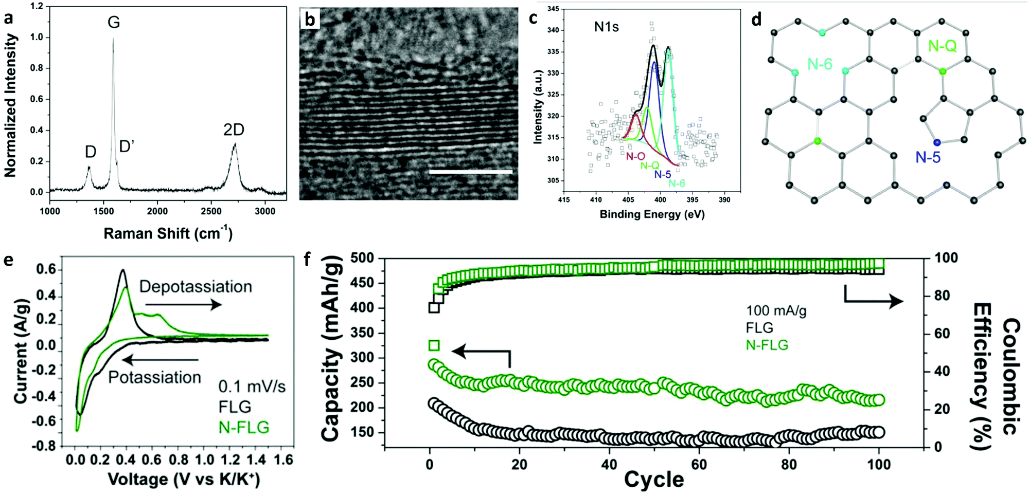 | ||
| Fig. 9 Structural characterization and electrochemical performance analysis of few-layer graphene doped with nitrogen (N-FLG) as an anode in a potassium-ion battery (KIB). (a) A Raman spectrum of N-FLG shows the typical peaks, where D and D′ are activated in the presence of nitrogen. (b) TEM of N-FLG confirms the layered structure (scale bar = 5 nm). (c) XPS data for the N 1s spectra with 4 peaks from different nitrogen bonding configurations. (d) Schematic illustration of different nitrogen defects in FLG. (e) Cyclic voltammetry of FLG and N-FLG reveals additional depotassiation peaks that contribute to the enhanced storage capacity of N-FLG. (f) Cycling abilities for both FLG and N-FLG exhibit a higher storage capacity and cyclability of N-FLG. Reproduced with permission.240 Copyright 2016, American Chemical Society. | ||
Functional phosphorus and oxygen dually-doped graphene (PODG) was introduced by Ma et al. as the anode for KIBs. They synthesized the PODG by thermal annealing of triphenylphosphine and graphite oxide precursors.241 The as-synthesized PODG showed long cycling stability and delivered a capacity of 474 mA h g−1 at 50 mA g−1 after 50 cycles. This electrode also exhibited a high rate capability of 160 mA h g−1 at 2000 mA g−1 after 600 cycles. The large interlayer spacing in the PODG, due to the introduction of phosphorus and oxygen, facilitated the K+ intercalation and delivered superior electrochemical performance.
These studies demonstrate that by incorporating nanomaterials into graphene it is possible to overcome the limitations of graphene anodes in KIBs.
Using DFT calculations, Xu et al. predicted that the theoretical capacity of single-layer silicene could reach up to 1196 mA h g−1 for Li+ ion storage.244 But, silicon-based electrodes show severe capacity fading due to their structural degradation and interfacial instability during lithiation and delithiation. To address the structural degradation and interface instability issues, Zhang et al. developed an intrinsically dually stabilized silicon building block, namely silicene flowers (SF).245 In the as-synthesized silicene flowers, thin silicene nanoplates accommodated the volume change of Si which ensured their structural stability (Fig. 10a). Besides, the presence of silicene nanoplates allowed shortened Li+ ion diffusion length and electron transport channels between the building blocks throughout the whole SF (Fig. 10b and c). As a result, SF exhibited a high gravimetric capacity of 2000 mA h g−1 at 800 mA g−1 as an anode in LIBs. They also showed an excellent rate capability of 950 mA h g−1 at 8 A g−1 and cycling stability of 1100 mA h g−1 at 2000 mA g−1 over 600 cycles (Fig. 10e). This study provided a promising insight into silicene for use as a high-performance electrode material in rechargeable batteries.
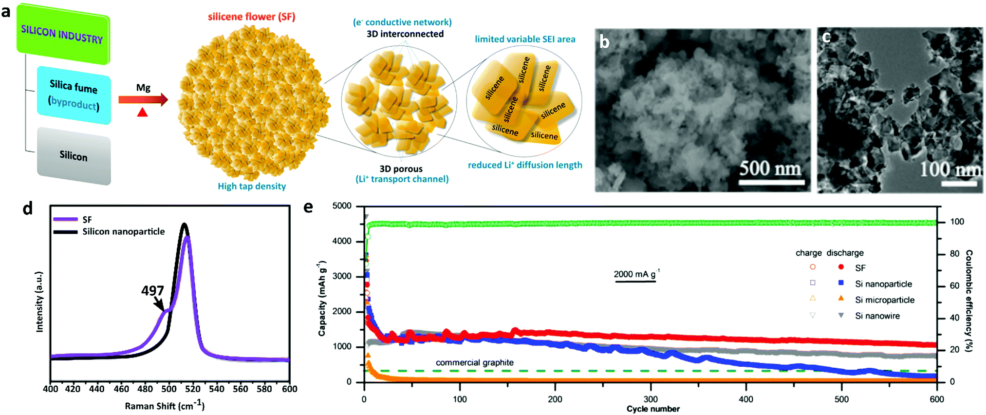 | ||
| Fig. 10 Structural characterization and electrochemical performance analysis of silicene flowers (SF) as an anode in a rechargeable battery. (a) Schematic illustration of SF synthesized by magnesiothermic reduction of silica fume at >850 °C. The synthesized SF block provides three-dimensional electron transport channels and reduces the Li+ ion diffusion length. (b) A SEM image shows the flower-like architecture of the SF with diameters ranging from ∼1 to 10 μm. (c) A TEM image reveals the interconnected nanoplatelets with interpenetrating pores (<20 nm) throughout the SF. (d) Raman spectra of the SF and silicon nanoparticles show an intense peak at 515 cm−1, which corresponds to the honeycomb silicene lattice. (e) The cycling performance profiles of the silicene flowers and Si particles over 600 cycles reveal the excellent cycling stability of the SF electrode at 2000 mA g−1. Reproduced with permission.245 Copyright 2017, American Chemical Society. | ||
In another approach, Shi et al. introduced graphene as a substrate with a silicene layer to prevent structural degradation during cycling.246Ab initio calculations showed that the silicene/graphene (Si/G) heterostructure maintained silicene's large capacity of 487 mA h g−1 for both LIBs and SIBs, and low diffusion energy barriers (<0.4 eV for Li and <0.3 eV for Na). The density of states results showed that the Si/G heterostructure is metallic, which provided a good electronic conductivity. The higher mechanical stiffness of the Si/G composite preserved the structural integrity of the anode and contributed to its better cycle performance.
Intrinsically metallic B-substituted silicene (BSi3) was reported as an anode material in LIBs by Tan et al.247 Using DFT calculations they showed that due to its unusual planar geometry and better electronic conductivity, metallic BSi3 silicene could provide a high theoretical capacity of 1410 mA h g−1.
Zhu et al. studied silicene for SIBs employing first-principles calculations.248 Freestanding silicene and a graphene–silicene superlattice were reported as electrode materials in SIBs. The calculated theoretical capacities were 954 mA h g−1 for freestanding silicene and 730 mA h g−1 for the graphene–silicene superlattice, which were higher than that of graphite. Besides, freestanding silicene showed an energy barrier of 0.16 eV for Na+ diffusion, which was significantly lower than that of graphene.
Silicene has also been evaluated as a potential cathode material in Li–S batteries. First-principles calculations showed that adsorption of lithium polysulfides (LiPS) on silicene was thermodynamically stable.249 S atoms anchored on the silicene surface could provide a theoretical capacity of 891 mA h g−1 without dissolution and migration of LiPS during cycling.250 This sulfur anchored silicene offered a constructive way to implement sulfur-based cathode materials for Li–S batteries with improved electrochemical performance.
Sharma et al. suggested that the adsorption of the Li atom at the hollow site of germanene was energetically favourable.57 The Bader charge analysis indicated ionic bonding between Li and Ge atoms and showed that the charge was transferred from the adsorbed Li atoms to germanene sheet. The calculated theoretical capacities for monolayer and bi-layer germanene were 369 mA h g−1 and 276 mA h g−1, respectively, as anodes in LIBs.
Zhu et al. proposed hybrid structures of germanene on semiconducting MgX2 (X = Cl, Br, and I) substrates as anodes in LIBs, based on first-principles calculations.252 They showed that Li did not cluster and the presence of MgX2 increased the Li+ ion storage capacity of germanene (279 mA h g−1 on MgCl2). A Li+ diffusion energy barrier of less than 0.25 eV was obtained for the hybrid structures.
In a different approach, Zhao et al. reported methyl terminated germanene (GeCH3) as an anode material for LIBs.253 They synthesized few-layer (4–5 mm thickness) GeCH3 nanosheets by liquid-phase exfoliation. A sandwiched GeCH3/rGO nanocomposite was also prepared by adding rGO as a conductive agent. GeCH3 exhibited a high initial capacity of 1202 mA h g−1 at 0.2 A g−1. The GeCH3/rGO nanocomposite exhibited a capacity of 2516 mA h g−1 initially and 1058 mA h g−1 after 100 cycles at 0.2 A g−1. The introduction of methyl groups increased the interlayer spacing of germanene and improved the stability, whereas rGO increased the electronic conductivity.
As an alternative to LIBs, Bhuvaneswari et al. studied the electronic properties of bare and hydrogenated germanene (BGe and HGe) nanosheets using density functional theory in SIBs.251 The negative magnitudes of the adsorption energies on Na+ on BGe and HGe indicated the strong surface assimilation of Na/Na+ on the germanene nanosheets. The density of states (DOS) spectrum and adsorption energy confirmed the stability of the germanene sheets as anodes for SIBs.
These studies suggest that germanene nanosheets can be used as anode materials in next generation metal-ion batteries and provide useful insights into how to evaluate germanene experimentally in the future.
Li et al. theoretically investigated the adsorption and diffusion behaviour of Li in both phosphorus and phosphorene.255 This study found that the diffusion energy barrier of Li+ in phosphorene was 0.08 eV along the zigzag direction, which was 102–104 times faster than that of graphene. The calculated average voltage of phosphorene in LIBs was predicted to be 2.9 V, higher than those of the existing anode materials. Moreover, intercalation of Li changed the semiconducting phosphorene to metallic phosphorene, which increased the electrical conductivity of the phosphorene electrode.
Kulish et al. systematically investigated phosphorene as an anode material for SIBs.255 They showed that at high Na concentration Na-phosphorene underwent semiconductor to metal transition similar to Li-phosphorene. Besides, the diffusion energy barrier of Na+ on phosphorene was 0.04 eV. As a result, phosphorene demonstrated a high theoretical specific capacity of up to 865 mA h g−1 (NaP). Nie et al. showed that the phosphorene electrode could deliver 2025 mA h g−1 with a 77% coulombic efficiency as shown in Fig. 11d.256 They performed in situ TEM and DFT calculations to show the charge transfer pathways for Na+ ions through the phosphorene layers. High resolution TEM (HRTEM) showed the atomically thin orientation of the phosphorene nanosheets as shown in Fig. 11a. Fig. 11b shows the structure evolution of phosphorene during the Na+ ion transport process along the [1 0 0] direction. The contact geometry between the phosphorene flakes and Na+ is shown by a schematic in Fig. 11c. Fig. 11d–f show the electrochemical performance of the phosphorene in the SIBs. The electrode showed a good cycling capability of 1820 mA h g−1 after 30 cycles at 100 mA g−1 and an excellent rate capability delivering 850 mA h g−1 at 2500 mA g−1. This study proved that Na+ ions preferably diffused along the [100] direction, and therefore, minimizing the dimension along the [010] direction of the phosphorene improved the performance of phosphorene for SIBs.
 | ||
| Fig. 11 Structural characterization and electrochemical performance analysis of phosphorene as an anode in a rechargeable battery. (a) HRTEM image of phosphorene viewed along the [001] direction with the corresponding fast Fourier transform in the inset. (b) An in situ TEM image shows the sodium transport process and the structure evolution of few-layer phosphorene. (c) The contact geometry shows that sodiation stripes along the [100] direction are formed between the phosphorene nanoflakes. (d) Galvanostatic discharge/charge curves of the phosphorene electrode at the rate of 100 mA g−1. (e) The cycling performance profiles show stable performance of phosphorene electrode. (f) Rate capacities of phosphorene at different current rates. Reproduced with permission.256 Copyright 2016, American Chemical Society. | ||
Sun et al. introduced a hybrid material of few layer phosphorene placed between graphene layers as an anode in SIBs.86 Here, the graphene layers acted as a buffer to volumetric expansion during cycling and also provided electrical paths, whereas the phosphorene layers offered a short path for Na+ ion diffusion during sodiation/desodiation processes. As a result, a high specific capacity of 2440 mA h g−1 at a current density of 0.05 A g−1 was achieved, which was 94% of the theoretical capacity of phosphorus. In situ TEM and ex situ XRD techniques revealed the formation of a Na3P alloy because of the intercalation of Na+ ions into the phosphorene layers. In another study, this hybrid phosphorene/graphene anode in SIBs delivered a high rate capability of 1120.6 mA h g−1 at 5 A g−1.257
Black phosphorus suffers from structural instability under ambient conditions, which limits the performance of phosphorus electrodes for LIBs.258 Chowdhury et al. introduced h-BN to cap black-phosphorene (Pn) and used it as an anode material in LIBs and SIBs. The binding energies of the h-BN/black-Pn heterostructure with lithium and sodium were greatly improved. As a result, the heterostructure electrode suffered a low volume change during charge/discharge processes. The heterostructure also underwent a phase transition from semiconductor to metal during lithiation and sodiation. As a result, high specific capacities of 607 and 445 mA h g−1 were achieved from the h-BN-capped black-Pn electrode, respectively, for LIBs and SIBs.
Han et al. systematically investigated phosphorene as an anode material using DFT for magnesium-ion batteries (MIBs).259 Their studies revealed that phosphorene bonded with Mg strongly in the cationic state. The diffusion energy barrier of Mg on phosphorene was only 0.09 eV along the zigzag direction, allowing fast and anisotropic diffusion of Mg+ ions. Therefore, the theoretical specific capacity of 865 mA h g−1 was achieved with an average voltage of 0.833 V as an anode in MIBs.
Given these advantages of high capacity, cycling stability, high ion mobility, and good electrical conductivity, monolayer phosphorene presents abundant opportunities as an anode material for metal-ion batteries.
Benzidi et al. employed DFT to investigate the interactions of Li, Na, and Mg ions with an arsenene monolayer to use it as an anode in metal-ion batteries.60 This study showed that the bonding of Li, Na, and Mg atoms with the arsenene monolayer was strong, which was beneficial for battery applications. The negative adsorption energies of Li, Na, and Mg ions on the valley sites were −2.55, −1.91, and −1.10 eV, respectively. Besides, arsenene showed high theoretical capacities of 1609.77, 1073.18, and 1430 mA h g−1 for Li, Na, and Mg, respectively, which were higher than the capacity of commercial graphite (372 mA h g−1) in LIBs. Besides, the diffusion energy barriers of the Li, Na, and Mg ions were calculated to be 0.16, 0.05, and 0.016 eV, respectively. In addition, Ab Initio Molecular Dynamics (AIMD) simulation showed that Li3As, Na2As, and Mg2As were reasonably stable at high temperatures (600 K).
Ye et al. reported arsenene as an alternative to pure Mg metal anodes.262 Mg anodes suffer from pulverization and sluggish diffusion of Mg2+ ions. Ye et al. employed first-principles calculations to show that Mg-adsorbed arsenene systems had good energetic stability. Mg was adsorbed on monolayer/bilayer arsenene and an arsenene/graphene heterostructure with adsorption energies of 0.82–2.48 eV, suggesting energetic stability of Mg-adsorbed arsenene. Monolayer arsenene exhibited low barriers (0.08–0.33 eV) for Mg diffusion and ∼3 times higher specific capacity (1429.41 mA h g−1) than the bilayer arsenene (536.60 mA h g−1) and the arsenene/graphene heterostructure (409.90 mA h g−1). Also, the volume changes were <16% during the magnesiation process, suggesting a good cycling reversibility.
For example, Sengupta et al. reported ab initio studies on the Li+ and Na+ adsorption properties of free-standing monolayer antimonene.263 Their study showed that antimonene as an anode material in SIBs provided a specific capacity of 320 mA h g−1, with a small diffusion barrier of 0.114 eV for Na atoms. For LIBs, antimonene provided a lower specific capacity of 208 mA h g−1 and also a higher diffusion barrier of 0.38 eV for Li atoms. The calculated high capacity and good Na+ diffusion can also be favourable for Na–air batteries and supercapacitors.
Su et al. showed that nano-scale modification is an alternative strategy to improve the cycling performance of Sb in LIBs.264 They systematically investigated the Li adsorption of monolayer antimonene using first-principles calculations based on vdW corrected DFT. β-Phase monolayer antimonene with a buckled hexagonal structure was selected for their calculation because of its higher thermodynamic stability as shown in Fig. 12a. The authors considered four typical adsorption sites (H, T1, T2, and B) for single Li atom, and showed that H, T1, and T2 had stable and favourable sites for Li adsorption (Fig. 12b). A calculation was shown for the change in adsorption energy and Bader charge with respect to Li concentration in LixSb. The adsorption energies increased from 1.70 eV to 1.91 eV, revealing the strong adsorption of Li on antimonene at high Li concentration. Furthermore, the almost constant Bader charge of Li suggested the formation of strong ion bonds at all concentration of Li atoms. A fast diffusion of Li atoms on antimonene was observed with a low energy barrier of 0.20 eV, whereas for bulk Sb the energy barrier was 1.73 eV (Fig. 12c). Antimonene also suffered relatively small volume change during lithiation, which could improve the cycling ability of the antimonene in LIBs. Gao et al. utilized tailored engineering to exfoliate β-phase antimonene from bulk Sb, and evaluated it experimentally as an anode in LIBs.265 Using ultrasonication with different power intensities, two types of tailored engineering, vertical direction and omnidirectional, were used to produce 2D antimonene and Sb nanoparticles (NPs). Both antimonene and antimony NPs exhibited stable electrochemical performances. Antimonene delivered 584.1 mA h g−1 and Sb NPs delivered 552.3 mA h g−1 after 100 cycles with the coulombic efficiencies close to 100% at 330 mA g−1, whereas the capacity of bulk Sb decreased significantly after 20 cycles. At a higher current density of 3300 mA g−1, antimonene exhibited a capacity of 488 mA h g−1, which also indicated its excellent high rate capability. Theoretical simulation revealed that the Li+ ion diffusion energy barrier for β-phase antimonene was 0.25 eV, which was smaller than the diffusion energy barrier (1.14 eV) of antimony. As a result, antimonene with large dimensions could provide cycling stability and high rate capability for LIBs, compared to its bulk counterparts.
 | ||
| Fig. 12 First-principles calculations of antimonene based on vdW corrected density functional theory (DFT) as an anode in a rechargeable battery. (a) Schematic illustration of the atomic structure of β-phase antimonene. (b) Schematic of four Li adsorption sites (H, T1, T2, B) on 2D antimonene. (c) Li+ ion diffusion and energy barriers in 2D antimonene layers. Reproduced with permission.264 Copyright 2018, Elsevier B.V. | ||
In another study, Wang et al. introduced graphene into antimonene to overcome the volume expansion and structural degradation of Sb alloy during lithiation.266 Their first-principles calculation results revealed that the graphene/antimonene (G/Sb) heterostructure had a negligible band gap of 0.06 eV, which was smaller than that of monolayer β-antimonene (1.24 eV). Thus, introducing graphene ensured high conductivity and fast electron transport in the G/Sb electrode during the charge/discharge process. Also, the volume expansion of the Li adsorbed G/Sb heterostructure was 1.2%, whereas it was 15% for monolayer β-antimonene. These results provided a good argument for the G/Sb heterostructure as an anode for LIBs.
Tian et al. evaluated the Na+ storage properties of 2D few-layer antimonene (FLA).63In situ synchrotron XRD and ex situ selected-area electron diffraction (SAED) showed that the FLA underwent a phase evolution during cycling which was completely reversible (Sb ![[left over right harpoons]](https://www.rsc.org/images/entities/char_21cb.gif) NaSb Na3Sb). The calculated Na+ diffusion energy barrier for FLA was 0.14 eV, which was smaller than that of graphene (0.22 eV). Due to this, the FLA maintained a stable capacity of 620 mA g−1 at 66 mA g−1 with a coulombic efficiency of 99.7% after 150 cycles and showed a high rate capability of 429 mA h g−1 at 3300 mA g−1. Compared to the theoretical capacity of Sb (660 mA h g−1), the FLA offered excellent potential as an anode in SIBs.
NaSb Na3Sb). The calculated Na+ diffusion energy barrier for FLA was 0.14 eV, which was smaller than that of graphene (0.22 eV). Due to this, the FLA maintained a stable capacity of 620 mA g−1 at 66 mA g−1 with a coulombic efficiency of 99.7% after 150 cycles and showed a high rate capability of 429 mA h g−1 at 3300 mA g−1. Compared to the theoretical capacity of Sb (660 mA h g−1), the FLA offered excellent potential as an anode in SIBs.
In another study recently, the adsorption of Na atoms on β-antimonene was studied by Upadhyay et al.267 Using first-principles calculation they showed that the semiconducting antimonene could acquire metallic nature after Na adsorption, leading to better conductivity and charge transfer in β-antimonene. The antimonene electrode was expected to be stable during sodiation. The study predicted that monolayer antimonene could adsorb three layers of Na, providing a maximum specific capacity of 421.63 mA h g−1.
These results suggest that elemental antimonene can be an interesting candidate as an anode material for rechargeable batteries with a large specific capacity, less volume expansion, a low diffusion barrier, excellent rate capability, and long cycling performance.
The adsorption energy of a single lithium atom on borophene was found to be −1.12 eV, which was enough to ensure stability during intercalation/deintercalation.269 The fully lithiated Li0.75B phase of borophene had a Li adsorption energy of −0.06 eV per atom. This study by Jiang et al. showed that Li0.75B corresponded to a theoretical specific capacity of 1860 mA h g−1. In addition, the diffusion energy barrier of 2.6 eV allowed faster diffusion of Li atoms along the path of corrugated borophene. AIMD simulations at 300 K also proved that the lithium atom could freely move along the path. More importantly, the metallic nature of borophene remained unchanged during the whole lithiation process, maintaining its excellent electronic conductivity.
Zhang et al. reported that borophene could be ideal for both Li+ and Na+ adsorption by using first-principles calculations.66 They showed that borophene maintained metallic characteristics and thus good electrical conductivity during both lithiation and sodiation. Besides, the small diffusion energy barrier of ∼0.3 eV for Na+ corresponded to a theoretical specific capacity of 1984 mA h g−1 in β12 borophene and 1240 mA h g−1 in χ3 borophene. It was found that the average open-circuit voltage of 0.53 V during sodiation/desodiation could effectively inhibit dendrite formation, and thus increase the energy density.270
Introducing vacancy defects or doping can further enhance the metallic nature of borophene. Lie et al. showed that a vacancy in the puckered structure of the borophene could introduce a dangling bond, and thus increase the Fermi level significantly.271 As a result, the metallic characteristics of the borophene became more prominent and excellent electrical conductivity was achieved. However, the defects in borophene weakened the Na+ adsorption on the surface. So, it is essential to control the generation of defects during the synthesis of borophene materials.
Given these advantages, borophene is considered to be a promising anode material for both LIBs and SIBs with high power density.
Borophene has also been studied as an anchoring material for sulfur cathodes in Li–S batteries.272,273 Borophene can effectively adsorb lithium polysulphides that are formed during discharge cycles and suppress the shuttle effect, resulting in improved utilization of the active material. Due to the high electrical conductivity and small deformation of borophene, borophene is a helpful host to the S cathode during charge/discharge processes. Particularly, defective borophene showed moderate adsorption energies of 1–3 eV. As a result, defective borophene could effectively suppress the shuttle effect, and also maintain the its shape during repeated lithiation/delithiation. According to these results, it is expected that borophene can also be a favourable anchoring material for Li–S batteries.
The performances of elemental 2D materials as electrode materials in various EESSs are presented in Table 1.
| Material | EESS, electrolyte chemistry | Voltage range (V) | Performancea | Ref. |
|---|---|---|---|---|
| a The cycling data are in the following form: specific capacity (mA h g−1)/cycle number/current density (mA g−1). b Capacity is in μA h cm−2. c C-rate. EMIMBF4, 1-ethyl-3-methylimidazolium tetrafluoroborate; EC, ethylene carbonate; PC, polypropylene carbonate; DEC, diethyl carbonate; DMC, dimethyl carbonate; FEC, fluoroethylene carbonate. | ||||
| Vacuum-assisted graphene | SC, EMIMBF4 | 0.01–4.0 | 284.5 F g−1/1 A g−1 | 274 |
| Hydrogen-annealed graphene | SC, EMIMBF4 | 0.1–4.0 | 306.03 F g−1/1 A g−1 | 275 |
| B-Doped graphene | LIB, 1 M LiPF6 in EC:DEC (1:1) |
0.01–3.0 | 1227/30/50 | 276 |
| Functionalized graphene framework | LIB, 1 M LiPF6 in EC:DMC:EMC (1:1:1) |
1.5–4.5 | 344/200/50 | 277 |
| I-Doped graphene | LIB, 1 M LiPF6 in EC:DEC (1:1) |
0.01–3.0 | 1565/200/100 | 278 |
| N,F-Codoped reduced graphene | LIB, 1 M LiPF6 in EC:DEC:EMC (1:1:1) |
0.01–3.0 | 344/500/2000 | 279 |
| Binder-free graphene | LIB, 1 M LiPF6 in EC:DMC (1:1) |
0.01–3.0 | 500/100/100 | 280 |
| Single-layered graphene | SIB, 1 M NaPF6 in EC:DEC (1:1) |
0.003–2.8 | 15.9/20/5b | 281 |
| Crumpled graphene paper | SIB, 1 M NaClO4 in PEC | 0.005–2.5 | 125/500/1000 | 282 |
| N-Doped graphene sheets | SIB, 1 M NaPF6 in EC:DMC (1:1) |
0.01–3.0 | 155.2/260/50 | 283 |
| N- and S-Doped graphene sheets | SIB, 1 M NaClO4 in EC:PC:FEC (1:1:0.02) |
0.01–3.0 | 289/100/100 | 284 |
| N-Doped graphene | KIB, 0.8 M KPF6 in EC:DEC (1:1) |
0.01–1.5 | 210/100/100 | 240 |
| Activated-crumpled graphene | KIB, 0.8 M KPF6 in EC:DEC (1:1) |
0.01–3.0 | 245/2800/500 | 285 |
| P,O-Codoped graphene | KIB, 0.8 M KPF6 in EC:DEC (1:1) |
0.01–3.0 | 160/600/2000 | 241 |
| Silicene sheets | LIB, 1 M LiPF6 in EC:DMC (1:1) |
0.05–3.0 | 149/10/50 | 286 |
| Silicene flowers | LIB, 1 M LiPF6 in EC:DEC (1:1) with 5% FEC |
0.01–2.0 | 1100/600/2000 | 245 |
| Germanene/rGO | LIB, 1 M LiPF6 in EC:DMC:DEC (1:1:1) with 2% FEC |
0.01–2.0 | 1058/100/200 | 253 |
| Hydrogenated germanene | LIB, 1 M LiPF6 in EC:DMC (1:1) |
0.01–2.5 | 341/100/1Cc | 287 |
| Phosphorene | Supercapacitor, 1 M H2SO4 | 0.01–0.8 | 684.3 F g−1/2.5 A g−1 | 199 |
| Phosphorene–graphene | LIB, 1 M LiPF6 in EC:DMC (1:1) |
0.01–3.0 | 432/800/500 | 288 |
| Phosphorene–graphene | SIB, 1 M NaClO4 in PC with 5% FEC | 0.02–1.5 | 1582.6/100/1000 | 257 |
| Few-layer phosphorene | SIB, 1 M NaClO4 in PC with 5% FEC | 0.02–1.5 | 603.3/100/1500 | 289 |
| Antimonene/SPE | SC, 0.5 M H2SO4 | 0.01–3.0 | 1578 F g−1/14 A g−1 | 200 |
| Antimonene/Mxene | SC, 1 M H2SO4 | 0.01–2.0 | 827.56 F cm−3/0.2 mA cm−2 | 290 |
5. Electrochemical applications beyond energy storage
5.1 Electrochemical sensing
Pristine graphene and its derivatives have been experimentally proven to have high sensitivities to various gas molecules. The 2D structure of graphene nanosheets ensures superior chemical sensing performance, such as high sensitivity and low noise, due to their high electron mobility and conductance at room temperature, high surface area-to-volume ratio, and fewer crystal defects.111 The extreme sensitivity of a single electron charge (or low concentration <1 ppb) is achievable with graphene at room temperature.111,291 In 2007, Schedin et al. prepared graphene microfabricated devices via micromechanical cleavage of graphite to detect various common gases (NO2, NH3, H2O, and CO). Their study showed outstanding sensor functionalities of graphene, such as the ultra-high sensitivity, fast and linear response to the adsorbates.111 Other researchers have investigated several more common or organic gases (e.g., H2,292 Cl2,293 CO2,294,295 CH3OH,291 C2H5OH,291 (CH2)4O,291 CHCl3,291 and CH3CN291) that are detectable via pristine graphene or rGO. Improved sensitivity or enrichment of adsorbate types can be achieved by surface functionalization (doping with nanoparticles at the surfaces) or by the introduction of defects into pristine graphene sheets.296Graphene-related studies fulfill the significant demand to develop gas sensors for extremely toxic compounds. Recent research focus has been extended to other graphene-like 2D materials since pristine graphene is unable to detect some toxic gases and common gases. Other elemental 2D materials have recently been proposed and synthesized. Although experimental studies on novel 2D materials have been limited to fundamental investigations of physical or chemical properties, numerous computational studies, especially DFT simulations, have predicted the gas-sensing properties of graphene-like materials (Table 2). The working principle of elemental 2D materials as gas sensors shares common factors with those of graphene and its well-known Dirac fermions. For example, silicene and germanene, which consist of group IV elements, have similar (to graphene) Dirac cone structures and tiny band gaps at the Dirac points. Once gas molecules are chemically adsorbed, charge-transfer occurs, leading to band gap opening at the Dirac points and changes in certain electrical properties, such as conductance.111 The working principle of gas sensing is presented in Fig. 13. The amount of opening is related to the number of molecules adsorbed, which enables highly accurate concentration measurements. This “band-gap engineering” often converts the material to a p-type or an n-type semiconductor sensor. Elements from different groups, such as B36 borophene with a graphene-like monolayer structure and a hexagonal vacancy at the center of the structure, follow the same principle.
 | ||
| Fig. 13 Working principle of gas sensing (left) and catalysis (right) of elemental 2D materials. Inspired from ref. 111 and 297. | ||
5.2 Catalysis
Electrochemical catalysis is another potential application for elemental 2D materials. The water-splitting reaction, which has been widely studied to produce a clean, renewable energy source, is governed by two core reactions, the hydrogen evolution reaction (HER) and the oxygen reduction reaction (ORR), which both require high catalytic performance.298 Because graphene has a high electron conductivity and surface area-to-volume ratio and is conventionally used as a carrier of other 2D or nanoparticle catalysts, Xie et al. proposed a fabrication method of pristine graphene single-layer and bi-layer electrodes on a SiO2 wafer for a catalysis application.297 The prepared electrodes showed stable HER catalytic performance for as long as 20 hours. The results suggest stability but less performance than highly oriented pyrolytic graphite. Due to the high chemical stability of pristine graphene, catalysts may not be able to deliver a better performance than Pt-based or other metallic catalysts without doping. However, the development of metal-free HER catalysts still provides beneficial abundance, durability and cost-effectiveness.298,299The catalytic activities of novel elemental 2D materials are limited to first-study stages such as gas-sensing applications. Gas adsorption investigations have provided some predictions of catalytic behavior.300,301 Catalytic behavior is primarily related to the adsorption and disassociation of certain elements (or chemical groups) on the surface of a 2D material, as shown in Fig. 13. For example, in computational studies, hydrogenation of CO2 is achieved via H2 dissociation and CO2 adsorption at the surface of silicene.301 However, adsorbed CO2 can eventually form carboxylic (COOH) species through multistep reactions with H species. The reduction of nitrobenzene (PhNO2) silicene to aniline (PhNH2) depends on N–O adsorption and dissociation.302
Another type of catalytic activity is predicted from the photocatalytic properties of semiconductors for the HER or ORR.303 As mentioned, the band-gap engineering of Dirac materials (silicene and germanene) can alter the redox potentials of the materials to reach an optimum position between the conduction band minimum and valence band maximum.
| Elemental 2D | DFT functional + basis set | Adsorbate | Adsorption energy, Ea (eV) | Band gap, Eg (meV) | Ref. |
|---|---|---|---|---|---|
| B3LYP: hybrid, Becke + Slater local + Hartree–Fock + Lee–Yang–Parr. GGA-PBE: generalized gradient approximation exchange, Perdew–Burke–Ernzerhof. LDA: local density approximation. | |||||
| Borophene | B3LYP+6-31G(d) | NO2 | −2.32 | — | 304 |
| B3LYP+6-31G(d) | NO | −1.79 | — | 304 | |
| B3LYP+6-31G(d) | NH3 | −1.75 | — | 304 | |
| B3LYP+6-31G(d) | CO2 | −0.36 | — | 304 | |
| B3LYP+6-31G(d) | CO | −1.38 | — | 304 | |
| B36 | B97D+6-31G(d) | HCOH | −10.5 to −1.2 | 360–980 | 305 |
| B36 | B97D+6-31G(d) | HCN | −0.55 to −0.50 | — | 306 |
| Silicene | GGA-PBE | NO2 | −1.53, −1.12 | 173, 168 | 307 |
| GGA-PBE | NO | −0.57 | 103 | 307 | |
| GGA-PBE | NH3 | −0.60 to −0.24 | 79–471 | 307 | |
| GGA-PBE, BLYP+LANL2DZ | CO | −0.99, −0.63 | — | 308 | |
| GGA-PBE | SO2 | −1.08 | — | 309 | |
| GGA-PBE | H2S | −0.212 | — | 309 | |
| Germanene | GGA-PBE | CO2 | −0.42 | — | 310 |
| GGA-PBE | SO2 | −1.56 | 140 | 310 | |
| GGA-PBE | H2S | −0.58 | 40 | 310 | |
| Phosphorene | GGA-PBE | NO2 | −0.63 | — | 166 |
| LDA | NH3 | −0.50 | — | 311 | |
| LDA | CO2 | −0.41 | — | 311 | |
| LDA | CO | −0.33 | — | 311 | |
| Arsenene | GGA-PBE | NO2 | −0.44 | — | 312 |
| GGA-PBE | SO2 | −0.34 | — | 312 | |
| GGA-PBE | NO | −0.15 | — | 313 | |
| GGA-PBE | NH3 | −0.16 | — | 313 | |
| GGA-PBE | N2 | −0.13 | — | 313 | |
| GGA-PBE | CO2 | −0.33 | — | 313 | |
| GGA-PBE | CO | −0.23 | — | 313 | |
| Antimonene | GGA-PBE | NO2 | −0.813 | — | 314 |
| GGA-PBE | NO | −0.416 | — | 314 | |
| GGA-PBE | NH3 | −0.407 | — | 314 | |
| GGA-PBE | SO2 | −0.467 | — | 314 | |
6. Conclusions
In conclusion, as mitigation of global greenhouse gas emission becomes a primary target, the development of robust, reliable, and economically feasible EESSs has achieved greater significance. Layered materials have shown promise to seamlessly overcome the drawbacks of conventional systems and advantageously impact EESSs. Because these materials have large interlayer spaces, improved electronic transport properties, and structural stability, they not only improve the performance and kinetics of existing state-of-the-art LIB systems, but they also provide reasonable and stable performances for systems that place excessive demands on electrode systems due to large ions, such as SIB and KIB systems. Due to their relatively low costs, these novel ESSs (e.g., SIB and KIB systems) offer potential electrical energy storage at the grid scale (MW h to GW h); therefore, application of layered materials as electrodes may quickly facilitate the transition to large-scale smart grid storage.Unlike graphene and TMDs, research on many mono-element 2D materials is still in its infancy. Many factors must be optimized, especially synthesis and successful scaling up, before mono-element 2D materials can be fully manifested in practical devices and EESSs. A significant quantity of research is being devoted, therefore, to increasing the understanding of the properties of these novel 2D materials, specifically phosphorene, antimonene, and silicene. However, considerable bottlenecks exist before they can be successfully commercialized, such as the successful scaling up of the synthesis for electrochemical applications, elucidating their structure–property relationships, and the systematic study of these materials for electrochemical, catalytic, and sensing applications. The first step towards the large-scale synthesis of elemental 2D materials would be to understand these materials at a fundamental level with more reliable and low-cost technologies. Secondly, strategies should be developed to mitigate the degradation of the materials and ensure the long-term stability of these materials in the environment. Finally, systematic studies should be carried out to establish a reliable statistical approach to understand the relationship and benefit of elemental 2D materials relative to their 3D counterparts. Greater innovation and research will lead to widespread deployment of these materials and help improve global energy.
Conflicts of interest
There are no conflicts to declare.Acknowledgements
This research was based on work supported by the National Science Foundation (CMMI NSF CAREER Award), grant no. 1454151.Notes and references
- S. Mukherjee, A. Bates, N. Schuppert, B. Son, J. G. Kim, J. S. Choi, M. J. Choi, D.-H. Lee, O. Kwon, J. Jasinski and S. Park, J. Power Sources, 2015, 286, 276–289 Search PubMed
.
- D. J. Wuebbles and A. K. Jain, Fuel Process. Technol., 2001, 71, 99–119 Search PubMed
- K. U. Rao and V. V. N. Kishore, Renewable Sustainable Energy Rev., 2010, 14, 1070–1078 Search PubMed
- S. Mukherjee, J. Turnley, E. Mansfield, J. Holm, D. Soares, L. David and G. Singh, R. Soc. Open Sci., 2019, 6(8), 190437 Search PubMed
- D. O. Akinyele and R. K. Rayudu, Sustainable Energy Technol. Assess., 2014, 8, 74–91 Search PubMed
- S. Mukherjee and G. Singh, ACS Appl. Energy Mater., 2019, 2, 932–955 Search PubMed
- D. Liu, Y. Wang, Y. Xie, L. He, J. Chen, K. Wu, R. Xu and Y. Gao, J. Power Sources, 2013, 232, 29–33 Search PubMed
- C. Delmas, Adv. Energy Mater., 2018, 8, 1703137 Search PubMed
- Y. Wang, R. Chen, T. Chen, H. Lv, G. Zhu, L. Ma, C. Wang, Z. Jin and J. Liu, Energy Storage Mater., 2016, 4, 103–129 Search PubMed
- S. Mukherjee, N. Schuppert, A. Bates, J. Jasinski, J.-E. Hong, M. J. Choi and S. Park, J. Power Sources, 2017, 347, 201–209 Search PubMed
- X. Fan, J. Mao, Y. Zhu, C. Luo, L. Suo, T. Gao, F. Han, S.-C. Liou and C. Wang, Adv. Energy Mater., 2015, 5, 1500174 Search PubMed
- J. He, Y. Wei, T. Zhai and H. Li, Mater. Chem. Front., 2018, 2, 437–455 Search PubMed
- M. D. Slater, D. Kim, E. Lee and C. S. Johnson, Adv. Funct. Mater., 2013, 23, 947–958 Search PubMed
- K. J. Harry, D. T. Hallinan, D. Y. Parkinson, A. A. MacDowell and N. P. Balsara, Nat. Mater., 2014, 13, 69–73 Search PubMed
- C. Daniel, D. Mohanty, J. Li and D. L. Wood, AIP Conf. Proc., 2014, 1597, 26–43 Search PubMed
- C. M. Julien, A. Mauger, K. Zaghib and H. Groult, Inorganics, 2014, 2, 132–154 Search PubMed
- M. Wakihara, Mater. Sci. Eng., R, 2001, 33, 109–134 Search PubMed
- A. M. Skundin, T. L. Kulova and A. B. Yaroslavtsev, Russ. J. Electrochem., 2018, 54, 113–152 Search PubMed
- H. Kim, J. E. Kwon, B. Lee, J. Hong, M. Lee, S. Y. Park and K. Kang, Chem. Mater., 2015, 27, 7258–7264 Search PubMed
- B. Garcia, S. Lavallée, G. Perron, C. Michot and M. Armand, Electrochim. Acta, 2004, 49, 4583–4588 Search PubMed
- D. Akinwande, C. J. Brennan, J. S. Bunch, P. Egberts, J. R. Felts, H. Gao, R. Huang, J.-S. Kim, T. Li, Y. Li, K. M. Liechti, N. Lu, H. S. Park, E. J. Reed, P. Wang, B. I. Yakobson, T. Zhang, Y.-W. Zhang, Y. Zhou and Y. Zhu, Extreme Mech. Lett., 2017, 13, 42–77 Search PubMed
- R. Mas-Ballesté, C. Gómez-Navarro, J. Gómez-Herrero and F. Zamora, Nanoscale, 2011, 3, 20–30 Search PubMed
- X. Zhang, L. Hou, A. Ciesielski and P. Samorì, Adv. Energy Mater., 2016, 6, 1600671 Search PubMed
- P. Zhang, F. Wang, M. Yu, X. Zhuang and X. Feng, Chem. Soc. Rev., 2018, 47, 7426–7451 Search PubMed
- Q. Ke and J. Wang, J. Materiomics, 2016, 2, 37–54 Search PubMed
- S. Manzeli, D. Ovchinnikov, D. Pasquier, O. V. Yazyev and A. Kis, Nat. Rev. Mater., 2017, 2, 17033 Search PubMed
- M. Pumera, Z. Sofer and A. Ambrosi, J. Mater. Chem. A, 2014, 2, 8981–8987 Search PubMed
- M. Velický and P. S. Toth, Appl. Mater. Today, 2017, 8, 68–103 Search PubMed
- D. Jariwala, T. J. Marks and M. C. Hersam, Nat. Mater., 2017, 16, 170–181 Search PubMed
- Y. Zhang, A. Rubio and G. L. Lay, J. Phys. D: Appl. Phys., 2017, 50, 053004 Search PubMed
- J. Lin, T. Yu, F. Han and G. Yang, Wiley Interdiscip. Rev.: Comput. Mol. Sci., 2020, e1473 Search PubMed
- P. May, U. Khan, J. M. Hughes and J. N. Coleman, J. Phys. Chem. C, 2012, 116, 11393–11400 Search PubMed
- G. Cunningham, M. Lotya, C. S. Cucinotta, S. Sanvito, S. D. Bergin, R. Menzel, M. S. P. Shaffer and J. N. Coleman, ACS Nano, 2012, 6, 3468–3480 Search PubMed
- S. Balendhran, S. Walia, H. Nili, S. Sriram and M. Bhaskaran, Small, 2015, 11, 640–652 Search PubMed
- Y. Zhang, A. Rubio and G. L. Lay, J. Phys. D: Appl. Phys., 2017, 50(5), 053004 Search PubMed
- H.-S. Tsai and J.-H. Liang, ChemNanoMat, 2017, 3, 604–613 Search PubMed
- J. Zhu and U. Schwingenschlögl, J. Mater. Chem. C, 2015, 3, 3946–3953 Search PubMed
- E. Lee, Y. S. Yoon and D.-J. Kim, ACS Sens., 2018, 3, 2045–2060 Search PubMed
- P. Vishnoi, K. Pramoda, U. Gupta, M. Chhetri, R. G. Balakrishna and C. N. R. Rao, ACS Appl. Mater. Interfaces, 2019, 11, 27780–27787 Search PubMed
- S. Mukherjee, Z. Ren and G. Singh, Nano-Micro Lett., 2018, 10, 70 Search PubMed
- C. Huo, Z. Yan, X. Song and H. Zeng, Sci. Bull., 2015, 60, 1994–2008 Search PubMed
- K. S. Novoselov, A. Mishchenko, A. Carvalho and A. H. Castro Neto, Science, 2016, 353, 461–473 Search PubMed
- H. Cui, Y. Guo, W. Ma and Z. Zhou, ChemSusChem, 2020, 13, 1155–1171 Search PubMed
- A. H. Castro Neto, F. Guinea, N. M. R. Peres, K. S. Novoselov and A. K. Geim, Rev. Mod. Phys., 2009, 81, 109–162 Search PubMed
-
A. K. Geim and K. S. Novoselov, Nanoscience and Technology, Macmillan Publishers Ltd, UK, 2009, pp. 11–19 DOI:10.1142/9789814287005_0002
- D. P. DiVincenzo and E. J. Mele, Phys. Rev. B: Condens. Matter Mater. Phys., 1984, 29, 1685–1694 Search PubMed
- Y. Shao, J. Wang, H. Wu, J. Liu, I. A. Aksay and Y. Lin, Electroanalysis, 2010, 22, 1027–1036 Search PubMed
- J. Xu, M. Wang, N. P. Wickramaratne, M. Jaroniec, S. Dou and L. Dai, Adv. Mater., 2015, 27, 2042–2048 Search PubMed
- Y. Liu, X. Dong and P. Chen, Chem. Soc. Rev., 2012, 41, 2283–2307 Search PubMed
- S. S. Varghese, S. Lonkar, K. K. Singh, S. Swaminathan and A. Abdala, Sens. Actuators, B, 2015, 218, 160–183 Search PubMed
- F.-f. Zhu, W.-j. Chen, Y. Xu, C.-l. Gao, D.-d. Guan, C.-h. Liu, D. Qian, S.-C. Zhang and J.-f. Jia, Nat. Mater., 2015, 14, 1020–1025 Search PubMed
- K. Takeda and K. Shiraishi, Phys. Rev. B: Condens. Matter Mater. Phys., 1994, 50, 14916–14922 Search PubMed
- G. G. Guzmán-Verri and L. C. Lew Yan Voon, Phys. Rev. B: Condens. Matter Mater. Phys., 2007, 76, 075131 Search PubMed
- B. Lalmi, H. Oughaddou, H. Enriquez, A. Kara, S. Vizzini, B. Ealet and B. Aufray, Appl. Phys. Lett., 2010, 97, 223109 Search PubMed
- J. Zhuang, X. Xu, G. Peleckis, W. Hao, S. X. Dou and Y. Du, Adv. Mater., 2017, 29, 1606716 Search PubMed
- A. Acun, L. Zhang, P. Bampoulis, M. Farmanbar, A. van Houselt, A. N. Rudenko, M. Lingenfelder, G. Brocks, B. Poelsema, M. I. Katsnelson and H. J. W. Zandvliet, J. Phys.: Condens. Matter, 2015, 27, 443002 Search PubMed
- D. K. Sharma, S. Kumar, A. Laref and S. Auluck, Comput. Condens. Matter, 2018, 16, e00314 Search PubMed
- S. Zhao, W. Kang and J. Xue, J. Mater. Chem. A, 2014, 2, 19046–19052 Search PubMed
- C. Liu, Y. Wang, J. Sun and A. Chen, Trans. Tianjin Univ., 2020, 26, 104–126 Search PubMed
- H. Benzidi, M. Lakhal, M. Garara, M. Abdellaoui, A. Benyoussef, A. El kenz and O. Mounkachi, Phys. Chem. Chem. Phys., 2019, 21, 19951–19962 Search PubMed
- P. Ares, F. Aguilar-Galindo, D. Rodríguez-San-Miguel, D. A. Aldave, S. Díaz-Tendero, M. Alcamí, F. Martín, J. Gómez-Herrero and F. Zamora, Adv. Mater., 2016, 28, 6332–6336 Search PubMed
- M. Pumera and Z. Sofer, Adv. Mater., 2017, 29, 1605299 Search PubMed
- W. Tian, S. Zhang, C. Huo, D. Zhu, Q. Li, L. Wang, X. Ren, L. Xie, S. Guo, P. K. Chu, H. Zeng and K. Huo, ACS Nano, 2018, 12, 1887–1893 Search PubMed
- Q. Zhong, L. Kong, J. Gou, W. Li, S. Sheng, S. Yang, P. Cheng, H. Li, K. Wu and L. Chen, Phys. Rev. Mater., 2017, 1, 021001 Search PubMed
- Z.-Q. Wang, T.-Y. Lü, H.-Q. Wang, Y. P. Feng and J.-C. Zheng, Front. Phys., 2019, 14, 33403 Search PubMed
- X. Zhang, J. Hu, Y. Cheng, H. Y. Yang, Y. Yao and S. A. Yang, Nanoscale, 2016, 8, 15340–15347 Search PubMed
- R. Pawlak, C. Drechsel, P. D’Astolfo, M. Kisiel, E. Meyer and J. I. Cerda, Proc. Natl. Acad. Sci. U. S. A., 2020, 117, 228 Search PubMed
- A. Saini, MRS Bull., 2014, 39, 393–394 Search PubMed
-
J. E. Proctor, D. M. Armada and A. Vijayaraghavan, An introduction to graphene and carbon nanotubes, CRC Press, 2017 Search PubMed
- C. Lee, X. Wei, J. W. Kysar and J. Hone, Science, 2008, 321, 385–388 Search PubMed
- P. Avouris, Z. Chen and V. Perebeinos, Nat. Nanotechnol., 2007, 2, 605–615 Search PubMed
- K. I. Bolotin, K. J. Sikes, Z. Jiang, M. Klima, G. Fudenberg, J. Hone, P. Kim and H. L. Stormer, Solid State Commun., 2008, 146, 351–355 Search PubMed
- R. R. Nair, P. Blake, A. N. Grigorenko, K. S. Novoselov, T. J. Booth, T. Stauber, N. M. R. Peres and A. K. Geim, Science, 2008, 320, 1308 Search PubMed
- S. Grimes and D. Du, Telecommun. Policy, 2020, 101959, DOI:10.1016/j.telpol.2020.101959
- M. Chhowalla, D. Jena and H. Zhang, Nat. Rev. Mater., 2016, 1, 16052 Search PubMed
- H. Okamoto, Y. Sugiyama and H. Nakano, Chem. – Eur. J., 2011, 17, 9864–9887 Search PubMed
- J. Wu, Y. Chen, J. Wu and K. Hippalgaonkar, Adv. Electron. Mater., 2018, 4, 1800248 Search PubMed
- S. Chowdhury and D. Jana, Rep. Prog. Phys., 2016, 79, 126501 Search PubMed
- L. Tao, E. Cinquanta, D. Chiappe, C. Grazianetti, M. Fanciulli, M. Dubey, A. Molle and D. Akinwande, Nat. Nanotechnol., 2015, 10, 227–231 Search PubMed
- S. Cahangirov, M. Topsakal, E. Aktürk, H. Şahin and S. Ciraci, Phys. Rev. Lett., 2009, 102, 236804 Search PubMed
- X. Kong, Q. Liu, C. Zhang, Z. Peng and Q. Chen, Chem. Soc. Rev., 2017, 46, 2127–2157 Search PubMed
- W. Tao, N. Kong, X. Ji, Y. Zhang, A. Sharma, J. Ouyang, B. Qi, J. Wang, N. Xie, C. Kang, H. Zhang, O. C. Farokhzad and J. S. Kim, Chem. Soc. Rev., 2019, 48, 2891–2912 Search PubMed
- B. Mortazavi, O. Rahaman, M. Makaremi, A. Dianat, G. Cuniberti and T. Rabczuk, Phys. E, 2017, 87, 228–232 Search PubMed
- B. Liu and K. Zhou, Prog. Mater. Sci., 2019, 100, 99–169 Search PubMed
- M. E. Dávila, L. Xian, S. Cahangirov, A. Rubio and G. Le Lay, New J. Phys., 2014, 16, 095002 Search PubMed
- J. Sun, H.-W. Lee, M. Pasta, H. Yuan, G. Zheng, Y. Sun, Y. Li and Y. Cui, Nat. Nanotechnol., 2015, 10, 980–985 Search PubMed
- H. Liu, A. T. Neal, Z. Zhu, Z. Luo, X. Xu, D. Tománek and P. D. Ye, ACS Nano, 2014, 8, 4033–4041 Search PubMed
- A. Carvalho, M. Wang, X. Zhu, A. S. Rodin, H. Su and A. H. Castro Neto, Nat. Rev. Mater., 2016, 1, 16061 Search PubMed
- J. L. Zhang, S. Zhao, C. Han, Z. Wang, S. Zhong, S. Sun, R. Guo, X. Zhou, C. D. Gu, K. D. Yuan, Z. Li and W. Chen, Nano Lett., 2016, 16, 4903–4908 Search PubMed
- L. Li, Y. Yu, G. J. Ye, Q. Ge, X. Ou, H. Wu, D. Feng, X. H. Chen and Y. Zhang, Nat. Nanotechnol., 2014, 9, 372–377 Search PubMed
- J. Qiao, X. Kong, Z.-X. Hu, F. Yang and W. Ji, Nat. Commun., 2014, 5, 4475 Search PubMed
- D. Çakır, H. Sahin and F. M. Peeters, Phys. Rev. B: Condens. Matter Mater. Phys., 2014, 90, 205421 Search PubMed
- C. Guhl, P. Kehne, Q. Ma, F. Tietz, P. Komissinskiy, W. Jaegermann and R. Hausbrand, Electrochim. Acta, 2018, 268, 226–233 Search PubMed
- H. Kim, J. C. Kim, S.-H. Bo, T. Shi, D.-H. Kwon and G. Ceder, Adv. Energy Mater., 2017, 7, 1700098 Search PubMed
- N. R. Glavin, R. Rao, V. Varshney, E. Bianco, A. Apte, A. Roy, E. Ringe and P. M. Ajayan, Adv. Mater., 2020, 32, 1904302 Search PubMed
- W. Zhou, J. Chen, P. Bai, S. Guo, S. Zhang, X. Song, L. Tao and H. Zeng, Research, 2019, 2019, 21 Search PubMed
- C. Kamal and M. Ezawa, Phys. Rev. B: Condens. Matter Mater. Phys., 2015, 91, 085423 Search PubMed
- S. Zhang, Z. Yan, Y. Li, Z. Chen and H. Zeng, Angew. Chem., Int. Ed., 2015, 54, 3112–3115 Search PubMed
- G. Moynihan, S. Sanvito and D. D. O’Regan, 2D Mater., 2017, 4, 045018 Search PubMed
- P. Vishnoi, M. Mazumder, S. K. Pati and C. N. R. Rao, New J. Chem., 2018, 42, 14091–14095 Search PubMed
- X. Kong, M. Gao, X.-W. Yan, Z.-Y. Lu and T. Xiang, Chin. Phys. B, 2018, 27, 046301 Search PubMed
- J. Shah, W. Wang, H. Sohail and R. Uhrberg, TDM, 2020, 7, 025013 Search PubMed
- O. Ü. Aktürk, V. O. Özçelik and S. Ciraci, Phys. Rev. B: Condens. Matter Mater. Phys., 2015, 91, 235446 Search PubMed
- Y. Xu, B. Peng, H. Zhang, H. Shao, R. Zhang and H. Zhu, Ann. Phys., 2017, 529, 1600152 Search PubMed
- A. J. Mannix, Z. Zhang, N. P. Guisinger, B. I. Yakobson and M. C. Hersam, Nat. Nanotechnol., 2018, 13, 444–450 Search PubMed
- A. J. Mannix, X.-F. Zhou, B. Kiraly, J. D. Wood, D. Alducin, B. D. Myers, X. Liu, B. L. Fisher, U. Santiago, J. R. Guest, M. J. Yacaman, A. Ponce, A. R. Oganov, M. C. Hersam and N. P. Guisinger, Science, 2015, 350, 1513–1516 Search PubMed
- K. S. Novoselov, A. K. Geim, S. V. Morozov, D. Jiang, Y. Zhang, S. V. Dubonos, I. V. Grigorieva and A. A. Firsov, Science, 2004, 306, 666–669 Search PubMed
- K. S. Novoselov, A. K. Geim, S. V. Morozov, D. Jiang, M. I. Katsnelson, I. V. Grigorieva, S. V. Dubonos and A. A. Firsov, Nature, 2005, 438, 197–200 Search PubMed
- K. S. Novoselov, D. Jiang, F. Schedin, T. J. Booth, V. V. Khotkevich, S. V. Morozov and A. K. Geim, Proc. Natl. Acad. Sci. U. S. A., 2005, 102, 10451–10453 Search PubMed
- Y. Zhang, Y.-W. Tan, H. L. Stormer and P. Kim, Nature, 2005, 438, 201–204 Search PubMed
- F. Schedin, A. K. Geim, S. V. Morozov, E. W. Hill, P. Blake, M. I. Katsnelson and K. S. Novoselov, Nat. Mater., 2007, 6, 652–655 Search PubMed
- A. A. Balandin, S. Ghosh, W. Bao, I. Calizo, D. Teweldebrhan, F. Miao and C. N. Lau, Nano Lett., 2008, 8, 902–907 Search PubMed
- M. D. Stoller, S. Park, Y. Zhu, J. An and R. S. Ruoff, Nano Lett., 2008, 8, 3498–3502 Search PubMed
- P. Vogt, P. De Padova, C. Quaresima, J. Avila, E. Frantzeskakis, M. C. Asensio, A. Resta, B. Ealet and G. Le Lay, Phys. Rev. Lett., 2012, 108, 155501 Search PubMed
- E. Bianco, S. Butler, S. Jiang, O. D. Restrepo, W. Windl and J. E. Goldberger, ACS Nano, 2013, 7, 4414–4421 Search PubMed
- R. Gusmão, Z. Sofer, D. Bouša and M. Pumera, Angew. Chem., Int. Ed., 2017, 56, 14318 Search PubMed
- J. Ji, X. Song, J. Liu, Z. Yan, C. Huo, S. Zhang, M. Su, L. Liao, W. Wang, Z. Ni, Y. Hao and H. Zeng, Nat. Commun., 2016, 7, 13352 Search PubMed
- P. Kumar, J. Singh and A. C. Pandey, RSC Adv., 2013, 3, 2313–2317 Search PubMed
- V. Kochat, A. Samanta, Y. Zhang, S. Bhowmick, P. Manimunda, S. A. S. Asif, A. S. Stender, R. Vajtai, A. K. Singh, C. S. Tiwary and P. M. Ajayan, Sci. Adv., 2018, 4, e1701373 Search PubMed
- V. Huc, N. Bendiab, N. Rosman, T. Ebbesen, C. Delacour and V. Bouchiat, Nanotechnology, 2008, 19, 455601 Search PubMed
- A. Shukla, R. Kumar, J. Mazher and A. Balan, Solid State Commun., 2009, 149, 718–721 Search PubMed
- G. S. Shmavonyan, G. Sevoyan and V. Aroutiounian, Arm. J. Phys., 2013, 6, 1–6 Search PubMed
- B.-J. Park, J.-S. Choi, J.-H. Eom, H. Ha, H. Y. Kim, S. Lee, H. Shin and S.-G. Yoon, ACS Nano, 2018, 12, 2008–2016 Search PubMed
- M. Lotya, Y. Hernandez, P. J. King, R. J. Smith, V. Nicolosi, L. S. Karlsson, F. M. Blighe, S. De, Z. Wang, I. T. McGovern, G. S. Duesberg and J. N. Coleman, J. Am. Chem. Soc., 2009, 131, 3611–3620 Search PubMed
- Z. Li, P. Wu, C. Wang, X. Fan, W. Zhang, X. Zhai, C. Zeng, Z. Li, J. Yang and J. Hou, ACS Nano, 2011, 5, 3385–3390 Search PubMed
- L. Li and M. Zhao, J. Phys. Chem. C, 2014, 118, 19129–19138 Search PubMed
- M. De Crescenzi, I. Berbezier, M. Scarselli, P. Castrucci, M. Abbarchi, A. Ronda, F. Jardali, J. Park and H. Vach, ACS Nano, 2016, 10, 11163–11171 Search PubMed
- M. Derivaz, D. Dentel, R. Stephan, M.-C. Hanf, A. Mehdaoui, P. Sonnet and C. Pirri, Nano Lett., 2015, 15, 2510–2516 Search PubMed
- S. Stankovich, D. A. Dikin, R. D. Piner, K. A. Kohlhaas, A. Kleinhammes, Y. Jia, Y. Wu, S. T. Nguyen and R. S. Ruoff, Carbon, 2007, 45, 1558–1565 Search PubMed
- Y. Hernandez, V. Nicolosi, M. Lotya, F. M. Blighe, Z. Sun, S. De, I. T. McGovern, B. Holland, M. Byrne, Y. K. Gun’Ko, J. J. Boland, P. Niraj, G. Duesberg, S. Krishnamurthy, R. Goodhue, J. Hutchison, V. Scardaci, A. C. Ferrari and J. N. Coleman, Nat. Nanotechnol., 2008, 3, 563–568 Search PubMed
- C. Liu, G. Hu and H. Gao, J. Supercrit. Fluids, 2012, 63, 99–104 Search PubMed
- Y. Si and E. T. Samulski, Nano Lett., 2008, 8, 1679–1682 Search PubMed
- V. C. Tung, M. J. Allen, Y. Yang and R. B. Kaner, Nat. Nanotechnol., 2009, 4, 25–29 Search PubMed
- Y. Sim, J. Park, Y. J. Kim, M.-J. Seong and S. Hong, J. Korean Phys. Soc., 2011, 58, 938–942 Search PubMed
- U. Khan, A. O’Neill, H. Porwal, P. May, K. Nawaz and J. N. Coleman, Carbon, 2012, 50, 470–475 Search PubMed
- P. R. Somani, S. P. Somani and M. Umeno, Chem. Phys. Lett., 2006, 430, 56–59 Search PubMed
- Q. Yu, J. Lian, S. Siriponglert, H. Li, Y. P. Chen and S.-S. Pei, Appl. Phys. Lett., 2008, 93, 113103 Search PubMed
- X. Wang, H. You, F. Liu, M. Li, L. Wan, S. Li, Q. Li, Y. Xu, R. Tian, Z. Yu, D. Xiang and J. Cheng, Chem. Vap. Deposition, 2009, 15, 53–56 Search PubMed
- Z. Sun, Z. Yan, J. Yao, E. Beitler, Y. Zhu and J. M. Tour, Nature, 2010, 468, 549–552 Search PubMed
- A. Guermoune, T. Chari, F. Popescu, S. S. Sabri, J. Guillemette, H. S. Skulason, T. Szkopek and M. Siaj, Carbon, 2011, 49, 4204–4210 Search PubMed
- X. Gan, H. Zhou, B. Zhu, X. Yu, Y. Jia, B. Sun, M. Zhang, X. Huang, J. Liu and T. Luo, Carbon, 2012, 50, 306–310 Search PubMed
- G. Ruan, Z. Sun, Z. Peng and J. M. Tour, ACS Nano, 2011, 5, 7601–7607 Search PubMed
- H. Sun, J. Xu, C. Wang, G. Ge, Y. Jia, J. Liu, F. Song and J. Wan, Carbon, 2016, 108, 356–362 Search PubMed
- X. Li, C. W. Magnuson, A. Venugopal, J. An, J. W. Suk, B. Han, M. Borysiak, W. Cai, A. Velamakanni, Y. Zhu, L. Fu, E. M. Vogel, E. Voelkl, L. Colombo and R. S. Ruoff, Nano Lett., 2010, 10, 4328–4334 Search PubMed
- Y. S. Kim, J. H. Lee, Y. D. Kim, S.-K. Jerng, K. Joo, E. Kim, J. Jung, E. Yoon, Y. D. Park, S. Seo and S.-H. Chun, Nanoscale, 2013, 5, 1221–1226 Search PubMed
- Y. Kim, W. Song, S. Y. Lee, C. Jeon, W. Jung, M. Kim and C. Y. Park, Appl. Phys. Lett., 2011, 98, 263106–2631063 Search PubMed
- L. Shi, K. Chen, R. Du, A. Bachmatiuk, M. H. Rümmeli, M. K. Priydarshi, Y. Zhang, A. Manivannan and Z. Liu, Small, 2015, 11, 6302–6308 Search PubMed
- Z. Chen, W. Ren, L. Gao, B. Liu, S. Pei and H.-M. Cheng, Nat. Mater., 2011, 10, 424–428 Search PubMed
- H. Nakano, T. Mitsuoka, M. Harada, K. Horibuchi, H. Nozaki, N. Takahashi, T. Nonaka, Y. Seno and H. Nakamura, Angew. Chem., Int. Ed., 2006, 45, 6303–6306 Search PubMed
- H. Okamoto, Y. Kumai, Y. Sugiyama, T. Mitsuoka, K. Nakanishi, T. Ohta, H. Nozaki, S. Yamaguchi, S. Shirai and H. Nakano, J. Am. Chem. Soc., 2010, 132, 2710–2718 Search PubMed
- A. Fleurence, R. Friedlein, T. Ozaki, H. Kawai, Y. Wang and Y. Yamada-Takamura, Phys. Rev. Lett., 2012, 108, 245501 Search PubMed
- L. Meng, Y. Wang, L. Zhang, S. Du, R. Wu, L. Li, Y. Zhang, G. Li, H. Zhou, W. A. Hofer and H.-J. Gao, Nano Lett., 2013, 13, 685–690 Search PubMed
- M. Neek-Amal, A. Sadeghi, G. R. Berdiyorov and F. M. Peeters, Appl. Phys. Lett., 2013, 103, 261904 Search PubMed
- T. Helbich, A. Lyuleeva, I. M. D. Höhlein, P. Marx, L. M. Scherf, J. Kehrle, T. F. Fässler, P. Lugli and B. Rieger, Chem. – Eur. J., 2016, 22, 6194–6198 Search PubMed
- K. Adpakpang, S. B. Patil, S. M. Oh, J.-H. Kang, M. Lacroix and S.-J. Hwang, Electrochim. Acta, 2016, 204, 60–68 Search PubMed
- L. Li, S.-Z. Lu, J. Pan, Z. Qin, Y.-Q. Wang, Y. Wang, G.-Y. Cao, S. Du and H.-J. Gao, Adv. Mater., 2014, 26, 4820–4824 Search PubMed
- L. Zhang, P. Bampoulis, A. N. Rudenko, Q. Yao, A. van Houselt, B. Poelsema, M. I. Katsnelson and H. J. W. Zandvliet, Phys. Rev. Lett., 2016, 116, 256804 Search PubMed
- M. Buscema, D. J. Groenendijk, S. I. Blanter, G. A. Steele, H. S. J. van der Zant and A. Castellanos-Gomez, Nano Lett., 2014, 14, 3347–3352 Search PubMed
- W. Lu, H. Nan, J. Hong, Y. Chen, C. Zhu, Z. Liang, X. Ma, Z. Ni, C. Jin and Z. Zhang, Nano Res., 2014, 7, 853–859 Search PubMed
- A. Castellanos-Gomez, L. Vicarelli, E. Prada, J. O. Island, K. L. Narasimha-Acharya, S. I. Blanter, D. J. Groenendijk, M. Buscema, G. A. Steele, J. V. Alvarez, H. W. Zandbergen, J. J. Palacios and H. S. J. van der Zant, 2D Mater., 2014, 1, 025001 Search PubMed
- D. Hanlon, C. Backes, E. Doherty, C. S. Cucinotta, N. C. Berner, C. Boland, K. Lee, A. Harvey, P. Lynch, Z. Gholamvand, S. Zhang, K. Wang, G. Moynihan, A. Pokle, Q. M. Ramasse, N. McEvoy, W. J. Blau, J. Wang, G. Abellan, F. Hauke, A. Hirsch, S. Sanvito, D. D. O’Regan, G. S. Duesberg, V. Nicolosi and J. N. Coleman, Nat. Commun., 2015, 6, 8563 Search PubMed
- A. H. Woomer, T. W. Farnsworth, J. Hu, R. A. Wells, C. L. Donley and S. C. Warren, ACS Nano, 2015, 9, 8869–8884 Search PubMed
- J. R. Brent, N. Savjani, E. A. Lewis, S. J. Haigh, D. J. Lewis and P. O’Brien, Chem. Commun., 2014, 50, 13338–13341 Search PubMed
- P. Yasaei, B. Kumar, T. Foroozan, C. Wang, M. Asadi, D. Tuschel, J. E. Indacochea, R. F. Klie and A. Salehi-Khojin, Adv. Mater., 2015, 27, 1887–1892 Search PubMed
- S. Zhang, J. Yang, R. Xu, F. Wang, W. Li, M. Ghufran, Y.-W. Zhang, Z. Yu, G. Zhang, Q. Qin and Y. Lu, ACS Nano, 2014, 8, 9590–9596 Search PubMed
- S. Cui, H. Pu, S. A. Wells, Z. Wen, S. Mao, J. Chang, M. C. Hersam and J. Chen, Nat. Commun., 2015, 6, 8632 Search PubMed
- E. Kovalska, N. Antonatos, J. Luxa and Z. Sofer, Inorg. Chem., 2020, 59(16), 11259–11265, DOI:10.1021/acs.inorgchem.0c00243
- Y. Shao, Z.-L. Liu, C. Cheng, X. Wu, H. Liu, C. Liu, J.-O. Wang, S.-Y. Zhu, Y.-Q. Wang, D.-X. Shi, K. Ibrahim, J.-T. Sun, Y.-L. Wang and H.-J. Gao, Nano Lett., 2018, 18, 2133–2139 Search PubMed
- H.-S. Tsai, S.-W. Wang, C.-H. Hsiao, C.-W. Chen, H. Ouyang, Y.-L. Chueh, H.-C. Kuo and J.-H. Liang, Chem. Mater., 2016, 28, 425–429 Search PubMed
- H.-S. Tsai, C.-W. Chen, C.-H. Hsiao, H. Ouyang and J.-H. Liang, Chem. Commun., 2016, 52, 8409–8412 Search PubMed
- C. Gibaja, D. Rodriguez-San-Miguel, P. Ares, J. Gómez-Herrero, M. Varela, R. Gillen, J. Maultzsch, F. Hauke, A. Hirsch, G. Abellán and F. Zamora, Angew. Chem., Int. Ed., 2016, 55, 14345–14349 Search PubMed
- A. R. Oganov, J. Chen, C. Gatti, Y. Ma, Y. Ma, C. W. Glass, Z. Liu, T. Yu, O. O. Kurakevych and V. L. Solozhenko, Nature, 2009, 457, 863–867 Search PubMed
- B. Feng, J. Zhang, Q. Zhong, W. Li, S. Li, H. Li, P. Cheng, S. Meng, L. Chen and K. Wu, Nat. Chem., 2016, 8, 563–568 Search PubMed
- B. Kiraly, X. Liu, L. Wang, Z. Zhang, A. J. Mannix, B. L. Fisher, B. I. Yakobson, M. C. Hersam and N. P. Guisinger, ACS Nano, 2019, 13, 3816–3822 Search PubMed
- G. Tai, T. Hu, Y. Zhou, X. Wang, J. Kong, T. Zeng, Y. You and Q. Wang, Angew. Chem., Int. Ed., 2015, 54, 15473–15477 Search PubMed
- X. Ji, N. Kong, J. Wang, W. Li, Y. Xiao, S. T. Gan, Y. Zhang, Y. Li, X. Song, Q. Xiong, S. Shi, Z. Li, W. Tao, H. Zhang, L. Mei and J. Shi, Adv. Mater., 2018, 30, 1803031 Search PubMed
- C. Tan, X. Cao, X.-J. Wu, Q. He, J. Yang, X. Zhang, J. Chen, W. Zhao, S. Han, G.-H. Nam, M. Sindoro and H. Zhang, Chem. Rev., 2017, 117, 6225–6331 Search PubMed
- D. Yu and L. Dai, J. Phys. Chem. Lett., 2010, 1, 467–470 Search PubMed
- Z. Lei, N. Christov and X. S. Zhao, Energy Environ. Sci., 2011, 4, 1866–1873 Search PubMed
- Y. Xu, Z. Lin, X. Zhong, X. Huang, N. O. Weiss, Y. Huang and X. Duan, Nat. Commun., 2014, 5, 4554 Search PubMed
- B. Mu, W. Zhang and A. Wang, J. Nanopart. Res., 2014, 16, 2432 Search PubMed
- H. Gómez, M. K. Ram, F. Alvi, P. Villalba, E. L. Stefanakos and A. Kumar, J. Power Sources, 2011, 196, 4102–4108 Search PubMed
- Y. Sun, Q. Wu, Y. Xu, H. Bai, C. Li and G. Shi, J. Mater. Chem., 2011, 21, 7154–7160 Search PubMed
- G. Wang, X. Sun, F. Lu, H. Sun, M. Yu, W. Jiang, C. Liu and J. Lian, Small, 2012, 8, 452–459 Search PubMed
- S.-M. Paek, E. Yoo and I. Honma, Nano Lett., 2009, 9, 72–75 Search PubMed
- X. Yang, J. Zhu, L. Qiu and D. Li, Adv. Mater., 2011, 23, 2833–2838 Search PubMed
- H. Chen, M. B. Müller, K. J. Gilmore, G. G. Wallace and D. Li, Adv. Mater., 2008, 20, 3557–3561 Search PubMed
- H.-P. Cong, X.-C. Ren, P. Wang and S.-H. Yu, ACS Nano, 2012, 6, 2693–2703 Search PubMed
- D. Su, Chem. Commun., 2012, 48, 7149–7151 Search PubMed
- Z.-S. Wu, Y. Sun, Y.-Z. Tan, S. Yang, X. Feng and K. Müllen, J. Am. Chem. Soc., 2012, 134, 19532–19535 Search PubMed
- G. Ning, Z. Fan, G. Wang, J. Gao, W. Qian and F. Wei, Chem. Commun., 2011, 47, 5976–5978 Search PubMed
- Q. Liao and C. Wang, CrystEngComm, 2019, 21, 662–672 Search PubMed
- J. Wei, C. Luo, H. Li, W. Lv, J. Liang, Y. Deng, Z. Huang, C. Wang, F. Kang and Q.-H. Yang, Carbon, 2019, 149, 492–498 Search PubMed
- Z. Xie, J. Zhu, Y. Bi, H. Ren, X. Chen and H. Yu, Phys. Status Solidi RRL, 2020, 14, 1900534 Search PubMed
- G. M. Yang, Q. Xu, X. Fan and W. T. Zheng, J. Phys. Chem. C, 2018, 122, 1903–1912 Search PubMed
- Q. Xu, G. M. Yang, X. Fan and W. T. Zheng, Phys. Chem. Chem. Phys., 2019, 21, 4276–4285 Search PubMed
- C. Hao, B. Yang, F. Wen, J. Xiang, L. Li, W. Wang, Z. Zeng, B. Xu, Z. Zhao, Z. Liu and Y. Tian, Adv. Mater., 2016, 28, 3194–3201 Search PubMed
- H. Xiao, Z.-S. Wu, L. Chen, F. Zhou, S. Zheng, W. Ren, H.-M. Cheng and X. Bao, ACS Nano, 2017, 11, 7284–7292 Search PubMed
- L. Zu, X. Gao, H. Lian, C. Li, Q. Liang, Y. Liang, X. Cui, Y. Liu, X. Wang and X. Cui, J. Alloys Compd., 2019, 770, 26–34 Search PubMed
- E. Martínez-Periñán, M. P. Down, C. Gibaja, E. Lorenzo, F. Zamora and C. E. Banks, Adv. Energy Mater., 2018, 8, 1702606 Search PubMed
- D. Li, Y. Chen, J. He, Q. Tang, C. Zhong and G. Ding, Chin. Phys. B, 2018, 27, 036303 Search PubMed
- M. Yoshio, H. Wang and K. Fukuda, Angew. Chem., Int. Ed., 2003, 42, 4203–4206 Search PubMed
- K. S. Novoselov, Z. Jiang, Y. Zhang, S. V. Morozov, H. L. Stormer, U. Zeitler, J. C. Maan, G. S. Boebinger, P. Kim and A. K. Geim, Science, 2007, 315, 1379 Search PubMed
- J. R. Dahn, T. Zheng, Y. Liu and J. S. Xue, Science, 1995, 270, 590–593 Search PubMed
- G. Wang, X. Shen, J. Yao and J. Park, Carbon, 2009, 47, 2049–2053 Search PubMed
- P. Guo, H. Song and X. Chen, Electrochem. Commun., 2009, 11, 1320–1324 Search PubMed
- B.-M. Goh, Y. Wang, M. V. Reddy, Y. L. Ding, L. Lu, C. Bunker and K. P. Loh, ACS Appl. Mater. Interfaces, 2014, 6, 9835–9841 Search PubMed
- H. Wang, L.-F. Cui, Y. Yang, H. Sanchez Casalongue, J. T. Robinson, Y. Liang, Y. Cui and H. Dai, J. Am. Chem. Soc., 2010, 132, 13978–13980 Search PubMed
- G. Zhou, D.-W. Wang, F. Li, L. Zhang, N. Li, Z.-S. Wu, L. Wen, G. Q. Lu and H.-M. Cheng, Chem. Mater., 2010, 22, 5306–5313 Search PubMed
- D. Wang, D. Choi, J. Li, Z. Yang, Z. Nie, R. Kou, D. Hu, C. Wang, L. V. Saraf, J. Zhang, I. A. Aksay and J. Liu, ACS Nano, 2009, 3, 907–914 Search PubMed
- M. Zhang, B. Qu, D. Lei, Y. Chen, X. Yu, L. Chen, Q. Li, Y. Wang and T. Wang, J. Mater. Chem., 2012, 22, 3868–3874 Search PubMed
- Z.-S. Wu, W. Ren, L. Wen, L. Gao, J. Zhao, Z. Chen, G. Zhou, F. Li and H.-M. Cheng, ACS Nano, 2010, 4, 3187–3194 Search PubMed
- L. Shen, C. Yuan, H. Luo, X. Zhang, S. Yang and X. Lu, Nanoscale, 2011, 3, 572–574 Search PubMed
- Y. J. Mai, S. J. Shi, D. Zhang, Y. Lu, C. D. Gu and J. P. Tu, J. Power Sources, 2012, 204, 155–161 Search PubMed
- Y. Chen, J. Zhu, B. Qu, B. Lu and Z. Xu, Nano Energy, 2014, 3, 88–94 Search PubMed
- L. Jiang, B. Lin, X. Li, X. Song, H. Xia, L. Li and H. Zeng, ACS Appl. Mater. Interfaces, 2016, 8, 2680–2687 Search PubMed
- J. Xia, L. Liu, J. Xie, H. Yan, Y. Yuan, M. Chen, C. Huang, Y. Zhang, S. Nie and X. Wang, Electrochim. Acta, 2018, 269, 452–461 Search PubMed
- S. Wu, R. Ge, M. Lu, R. Xu and Z. Zhang, Nano Energy, 2015, 15, 379–405 Search PubMed
- N. Li, M. Zheng, H. Lu, Z. Hu, C. Shen, X. Chang, G. Ji, J. Cao and Y. Shi, Chem. Commun., 2012, 48, 4106–4108 Search PubMed
- X. Zhou, J. Xie, J. Yang, Y. Zou, J. Tang, S. Wang, L. Ma and Q. Liao, J. Power Sources, 2013, 243, 993–1000 Search PubMed
- J. Huang, Z. Xu, L. Cao, Q. Zhang, H. Ouyang and J. Li, Energy Technol., 2015, 3, 1108–1114 Search PubMed
- Y. Qiu, W. Li, W. Zhao, G. Li, Y. Hou, M. Liu, L. Zhou, F. Ye, H. Li, Z. Wei, S. Yang, W. Duan, Y. Ye, J. Guo and Y. Zhang, Nano Lett., 2014, 14, 4821–4827 Search PubMed
- B. Ding, C. Yuan, L. Shen, G. Xu, P. Nie, Q. Lai and X. Zhang, J. Mater. Chem. A, 2013, 1, 1096–1101 Search PubMed
- Y. Lu, Y. Lu, Z. Niu and J. Chen, Adv. Energy Mater., 2018, 8, 1702469 Search PubMed
- Y.-X. Wang, S.-L. Chou, H.-K. Liu and S.-X. Dou, Carbon, 2013, 57, 202–208 Search PubMed
- S. Mukherjee, S. Bin Mujib, D. Soares and G. Singh, Materials, 2019, 12, 1952 Search PubMed
- H. A. Cha, H. M. Jeong and J. K. Kang, J. Mater. Chem. A, 2014, 2, 5182–5186 Search PubMed
- T. Li, A. Qin, L. Yang, J. Chen, Q. Wang, D. Zhang and H. Yang, ACS Appl. Mater. Interfaces, 2017, 9, 19900–19907 Search PubMed
- Z. Li, J. Ding and D. Mitlin, Acc. Chem. Res., 2015, 48, 1657–1665 Search PubMed
- K. Xie, K. Yuan, X. Li, W. Lu, C. Shen, C. Liang, R. Vajtai, P. Ajayan and B. Wei, Small, 2017, 13, 1701471 Search PubMed
- D. Li, D. Yan, X. Zhang, J. Li, T. Lu and L. Pan, J. Colloid Interface Sci., 2017, 497, 350–358 Search PubMed
- D. Li, D. Yan, J. Ma, W. Qin, X. Zhang, T. Lu and L. Pan, Ceram. Int., 2016, 42, 15634–15642 Search PubMed
- S. Zhang, W. Li, B. Tan, S. Chou, Z. Li and S. Dou, J. Mater. Chem. A, 2015, 3, 4793–4798 Search PubMed
- Y. Liu, Z. Cheng, H. Sun, H. Arandiyan, J. Li and M. Ahmad, J. Power Sources, 2015, 273, 878–884 Search PubMed
- D. Su and G. Wang, ACS Nano, 2013, 7, 11218–11226 Search PubMed
- H. Lai, B. Feng, Y. Jiang, N. Shi, C. Liang, S. Chang, S. Guo, B. Cui and H. Cao, Mater. Lett., 2016, 166, 292–295 Search PubMed
- D. Su, H.-J. Ahn and G. Wang, Chem. Commun., 2013, 49, 3131–3133 Search PubMed
- L. David, R. Bhandavat and G. Singh, ACS Nano, 2014, 8, 1759–1770 Search PubMed
- X. Xie, D. Su, S. Chen, J. Zhang, S. Dou and G. Wang, Chem. – Asian J., 2014, 9, 1611–1617 Search PubMed
- K. Share, A. P. Cohn, R. Carter, B. Rogers and C. L. Pint, ACS Nano, 2016, 10, 9738–9744 Search PubMed
- G. Ma, K. Huang, J.-S. Ma, Z. Ju, Z. Xing and Q.-C. Zhuang, J. Mater. Chem. A, 2017, 5, 7854–7861 Search PubMed
- G. A. Tritsaris, E. Kaxiras, S. Meng and E. Wang, Nano Lett., 2013, 13, 2258–2263 Search PubMed
- J. Deng, J. Z. Liu and N. V. Medhekar, RSC Adv., 2013, 3, 20338–20344 Search PubMed
- S. Xu, X. Fan, J. Liu, D. J. Singh, Q. Jiang and W. Zheng, Phys. Chem. Chem. Phys., 2018, 20, 8887–8896 Search PubMed
- X. Zhang, X. Qiu, D. Kong, L. Zhou, Z. Li, X. Li and L. Zhi, ACS Nano, 2017, 11, 7476–7484 Search PubMed
- L. Shi, T. S. Zhao, A. Xu and J. B. Xu, J. Mater. Chem. A, 2016, 4, 16377–16382 Search PubMed
- X. Tan, C. R. Cabrera and Z. Chen, J. Phys. Chem. C, 2014, 118, 25836–25843 Search PubMed
- J. Zhu and U. Schwingenschlögl, 2D Mater., 2016, 3, 035012 Search PubMed
- Z. Liu, P. B. Balbuena and P. P. Mukherjee, J. Coord. Chem., 2016, 69, 2090–2105 Search PubMed
- F. Li and J. Zhao, ACS Appl. Mater. Interfaces, 2017, 9, 42836–42844 Search PubMed
- R. Bhuvaneswari, V. Nagarajan and R. Chandiramouli, Mater. Res. Express, 2018, 6, 035504 Search PubMed
- J. Zhu, A. Chroneos and U. Schwingenschlögl, Nanoscale, 2016, 8, 7272–7277 Search PubMed
- F. Zhao, Y. Wang, X. Zhang, X. Liang, F. Zhang, L. Wang, Y. Li, Y. Feng and W. Feng, Carbon, 2020, 161, 287–298 Search PubMed
- C. Zhang, M. Yu, G. Anderson, R. R. Dharmasena and G. Sumanasekera, Nanotechnology, 2017, 28, 075401 Search PubMed
- V. V. Kulish, O. I. Malyi, C. Persson and P. Wu, Phys. Chem. Chem. Phys., 2015, 17, 13921–13928 Search PubMed
- A. Nie, Y. Cheng, S. Ning, T. Foroozan, P. Yasaei, W. Li, B. Song, Y. Yuan, L. Chen, A. Salehi-Khojin, F. Mashayek and R. Shahbazian-Yassar, Nano Lett., 2016, 16, 2240–2247 Search PubMed
- H. Shuai, P. Ge, W. Hong, S. Li, J. Hu, H. Hou, G. Zou and X. Ji, Small Methods, 2019, 3, 1800328 Search PubMed
- C. Chowdhury, S. Karmakar and A. Datta, ACS Energy Lett., 2016, 1, 253–259 Search PubMed
- X. Han, C. Liu, J. Sun, A. D. Sendek and W. Yang, RSC Adv., 2018, 8, 7196–7204 Search PubMed
- Y. Wang and Y. Ding, Nanoscale Res. Lett., 2015, 10, 254 Search PubMed
- Z. Li, W. Xu, Y. Yu, H. Du, K. Zhen, J. Wang, L. Luo, H. Qiu and X. Yang, J. Mater. Chem. C, 2016, 4, 362–370 Search PubMed
- X.-J. Ye, G.-L. Zhu, J. Liu, C.-S. Liu and X.-H. Yan, J. Phys. Chem. C, 2019, 123, 15777–15786 Search PubMed
- A. Sengupta and T. Frauenheim, Mater. Today Energy, 2017, 5, 347–354 Search PubMed
- J. Su, T. Duan, W. Li, B. Xiao, G. Zhou, Y. Pei and X. Wang, Appl. Surf. Sci., 2018, 462, 270–275 Search PubMed
- Y. Gao, W. Tian, C. Huo, K. Zhang, S. Guo, S. Zhang, X. Song, L. Jiang, K. Huo and H. Zeng, J. Mater. Chem. A, 2019, 7, 3238–3243 Search PubMed
- X. Wang, C. Tang, X. Zhou, W. Zhu and C. Cheng, Appl. Surf. Sci., 2019, 491, 451–459 Search PubMed
- S. Upadhyay and P. Srivastava, Mater. Chem. Phys., 2020, 241, 122381 Search PubMed
- B. Mortazavi, A. Dianat, O. Rahaman, G. Cuniberti and T. Rabczuk, J. Power Sources, 2016, 329, 456–461 Search PubMed
- H. Jiang, Z. Lu, M. Wu, F. Ciucci and T. Zhao, Nano Energy, 2016, 23, 97–104 Search PubMed
- L. Shi, T. Zhao, A. Xu and J. Xu, Sci. Bull., 2016, 61, 1138–1144 Search PubMed
- J. Liu, C. Zhang, L. Xu and S. Ju, RSC Adv., 2018, 8, 17773–17785 Search PubMed
- S. Grixti, S. Mukherjee and C. V. Singh, Energy Storage Mater., 2018, 13, 80–87 Search PubMed
- H. R. Jiang, W. Shyy, M. Liu, Y. X. Ren and T. S. Zhao, J. Mater. Chem. A, 2018, 6, 2107–2114 Search PubMed
- H. Yang, S. Kannappan, A. S. Pandian, J.-H. Jang, Y. S. Lee and W. Lu, J. Power Sources, 2015, 284, 146–153 Search PubMed
- H. Yang, S. Kannappan, A. S. Pandian, J.-H. Jang, Y. S. Lee and W. Lu, Nanotechnology, 2017, 28, 445401 Search PubMed
- Z.-S. Wu, W. Ren, L. Xu, F. Li and H.-M. Cheng, ACS Nano, 2011, 5, 5463–5471 Search PubMed
- D. Xiong, X. Li, Z. Bai, H. Shan, L. Fan, C. Wu, D. Li and S. Lu, ACS Appl. Mater. Interfaces, 2017, 9, 10643–10651 Search PubMed
- Y. Zhan, B. Zhang, L. Cao, X. Wu, Z. Lin, X. Yu, X. Zhang, D. Zeng, F. Xie, W. Zhang, J. Chen and H. Meng, Carbon, 2015, 94, 1–8 Search PubMed
- S. Liu, W. Wei, C. Luo, Y. Wang and J. Ren, J. Phys. Chem. C, 2020, 124, 16739–16747 Search PubMed
- H. Sun, A. E. Del Rio Castillo, S. Monaco, A. Capasso, A. Ansaldo, M. Prato, D. A. Dinh, V. Pellegrini, B. Scrosati, L. Manna and F. Bonaccorso, J. Mater. Chem. A, 2016, 4, 6886–6895 Search PubMed
- A. Ramos, I. Cameán, N. Cuesta and A. B. García, Electrochim. Acta, 2015, 178, 392–397 Search PubMed
- Y. S. Yun, Y.-U. Park, S.-J. Chang, B. H. Kim, J. Choi, J. Wang, D. Zhang, P. V. Braun, H.-J. Jin and K. Kang, Carbon, 2016, 99, 658–664 Search PubMed
- H.-g. Wang, Z. Wu, F.-l. Meng, D.-l. Ma, X.-l. Huang, L.-m. Wang and X.-b. Zhang, ChemSusChem, 2013, 6, 56–60 Search PubMed
- Y. Ma, Q. Guo, M. Yang, Y. Wang, T. Chen, Q. Chen, X. Zhu, Q. Xia, S. Li and H. Xia, Energy Storage Mater., 2018, 13, 134–141 Search PubMed
- B. Lee, M. Kim, S. Kim, J. Nanda, S. J. Kwon, H. D. Jang, D. Mitlin and S. W. Lee, Adv. Energy Mater., 2020, 10, 1903280 Search PubMed
- M. Nematzadeh, A. Massoudi and M. Nangir, Mater. Today: Proc., 2020 DOI:10.1016/j.matpr.2020.03.210
- A. C. Serino, J. S. Ko, M. T. Yeung, J. J. Schwartz, C. B. Kang, S. H. Tolbert, R. B. Kaner, B. S. Dunn and P. S. Weiss, ACS Nano, 2017, 11, 7995–8001 Search PubMed
- Y. Zhang, H. Wang, Z. Luo, H. T. Tan, B. Li, S. Sun, Z. Li, Y. Zong, Z. J. Xu, Y. Yang, K. A. Khor and Q. Yan, Adv. Energy Mater., 2016, 6, 1600453 Search PubMed
- Z. Huang, H. Hou, Y. Zhang, C. Wang, X. Qiu and X. Ji, Adv. Mater., 2017, 29, 1702372 Search PubMed
- J. Yu, J. Zhou, P. Yao, H. Xie, M. Zhang, M. Ji, H. Liu, Q. Liu, C. Zhu and J. Xu, Adv. Energy Mater., 2019, 9, 1902462 Search PubMed
- S. Rumyantsev, G. Liu, M. S. Shur, R. A. Potyrailo and A. A. Balandin, Nano Lett., 2012, 12, 2294–2298 Search PubMed
- R. Arsat, M. Breedon, M. Shafiei, P. G. Spizziri, S. Gilje, R. B. Kaner, K. Kalantar-zadeh and W. Wlodarski, Chem. Phys. Lett., 2009, 467, 344–347 Search PubMed
- V. Dua, S. P. Surwade, S. Ammu, S. R. Agnihotra, S. Jain, K. E. Roberts, S. Park, R. S. Ruoff and S. K. Manohar, Angew. Chem., Int. Ed., 2010, 49, 2154–2157 Search PubMed
- H. J. Yoon, D. H. Jun, J. H. Yang, Z. Zhou, S. S. Yang and M. M.-C. Cheng, Sens. Actuators, B, 2011, 157, 310–313 Search PubMed
- S. M. Hafiz, R. Ritikos, T. J. Whitcher, N. M. Razib, D. C. S. Bien, N. Chanlek, H. Nakajima, T. Saisopa, P. Songsiriritthigul, N. M. Huang and S. A. Rahman, Sens. Actuators, B, 2014, 193, 692–700 Search PubMed
- S. G. Chatterjee, S. Chatterjee, A. K. Ray and A. K. Chakraborty, Sens. Actuators, B, 2015, 221, 1170–1181 Search PubMed
- A. Xie, N. Xuan, K. Ba and Z. Sun, ACS Appl. Mater. Interfaces, 2017, 9, 4643–4648 Search PubMed
- S. S. Shinde, A. Sami and J.-H. Lee, Electrochim. Acta, 2016, 214, 173–181 Search PubMed
- H. Jiang, Y. Zhu, Y. Su, Y. Yao, Y. Liu, X. Yang and C. Li, J. Mater. Chem. A, 2015, 3, 12642–12645 Search PubMed
- G. K. Walia and D. K. K. Randhawa, J. Mol. Model., 2018, 24, 242 Search PubMed
- S. Zhou, W. Pei, J. Zhao and A. Du, Nanoscale, 2019, 11, 7734–7743 Search PubMed
- C. Morrissey and H. He, Chem. Phys. Lett., 2018, 695, 228–234 Search PubMed
- C. J. Rupp, S. Chakraborty, J. Anversa, R. J. Baierle and R. Ahuja, ACS Appl. Mater. Interfaces, 2016, 8, 1536–1544 Search PubMed
- V. Shukla, J. Wärnå, N. K. Jena, A. Grigoriev and R. Ahuja, J. Phys. Chem. C, 2017, 121, 26869–26876 Search PubMed
- A. Shahbazi Kootenaei and G. Ansari, Phys. Lett. A, 2016, 380, 2664–2668 Search PubMed
- A. Omidvar, Comput. Theor. Chem., 2017, 1115, 179–184 Search PubMed
- W. Hu, N. Xia, X. Wu, Z. Li and J. Yang, Phys. Chem. Chem. Phys., 2014, 16, 6957–6962 Search PubMed
- T. H. Osborn and A. A. Farajian, Nano Res., 2014, 7, 945–952 Search PubMed
- S. M. Aghaei, M. M. Monshi and I. Calizo, RSC Adv., 2016, 6, 94417–94428 Search PubMed
- M. M. Monshi, S. M. Aghaei and I. Calizo, Surf. Sci., 2017, 665, 96–102 Search PubMed
- L. Kou, T. Frauenheim and C. Chen, J. Phys. Chem. Lett., 2014, 5, 2675–2681 Search PubMed
- X. Chen, L. Wang, X. Sun, R. Meng, J. Xiao, H. Ye and G. Zhang, IEEE Electron Device Lett., 2017, 38, 661–664 Search PubMed
- C. Liu, C.-S. Liu and X. Yan, Phys. Lett. A, 2017, 381, 1092–1096 Search PubMed
- R. Meng, M. Cai, J. Jiang, Q. Liang, X. Sun, Q. Yang, C. Tan and X. Chen, IEEE Electron Device Lett., 2017, 38, 134–137 Search PubMed
Footnote |
| † Equal contribution. |
| This journal is © The Royal Society of Chemistry 2020 |